

Page 1
12/21/2018 chipKIT DP32 Reference Manual [Reference.Digilentinc]
(https://reference.digilentinc.com/_detail/chipkit_dp32/16025616573_29ae205bbe_z.jpg?id=chipkit_dp32%3Arefmanual)
Revised March, 2015
This manual primarily applies to Rev C, as found on the underside of the board next to the white bar-coded box. Rev C is a major change
from Rev B, so differences will be noted where appropriate.
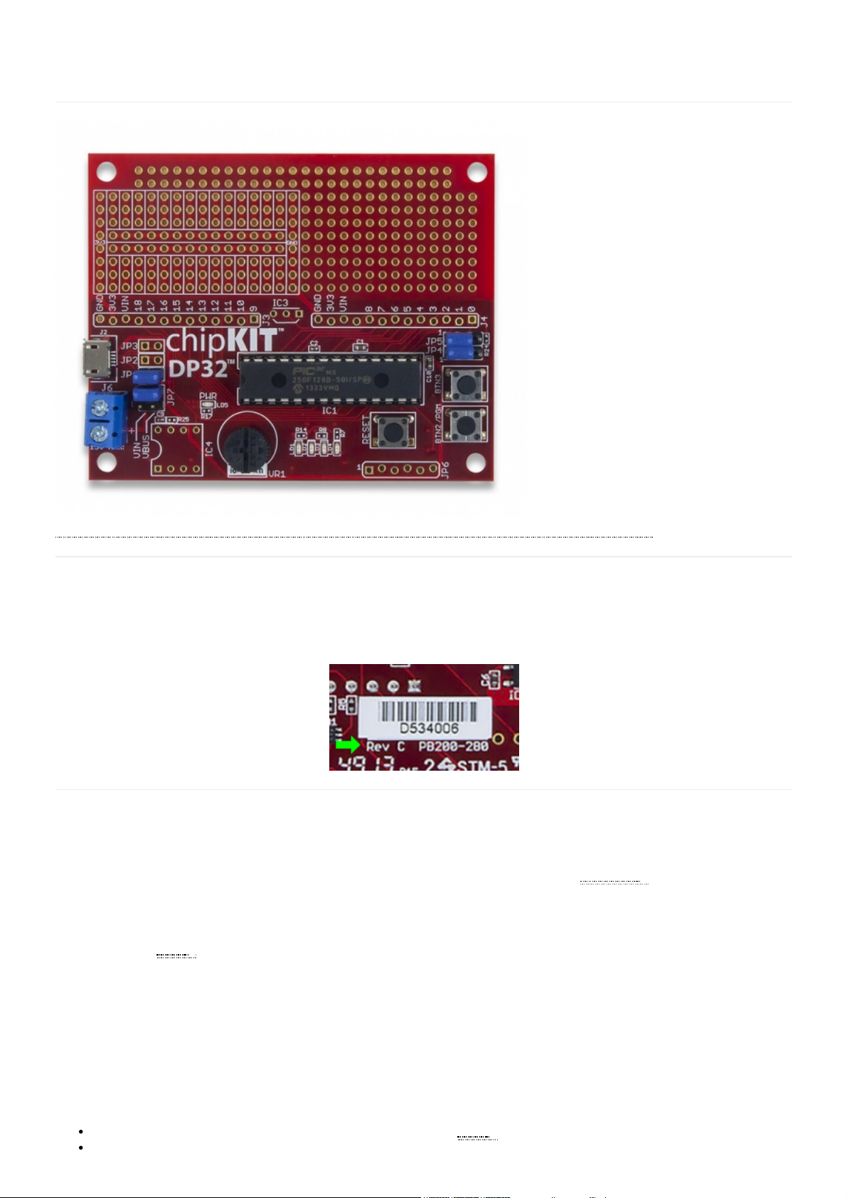
The chipKIT DP32 is an MPIDE compatible prototyping and project development board from Digilent. It combines the power of the
Microchip® PIC32MX250F128B 28-pin DIP with a wire wrap prototyping area, provision for an EEPROM () non-volatile memory, and
analog temperature sensor, a potentiometer, buttons and LEDs in a single board. The mounting hole footprint on the board is designed
to fit in the Hammond 1591XXSSBK project box.
The DP32 takes advantage of the powerful PIC32MX250F128B microcontroller. This microcontroller features a 32-bit MIPS processor
core running at 40 MHz (), 128K of flash program memory and 32K of SRAM data memory. It is suitable for building projects directly
on the board utilizing the provided prototyping area, but it can also be used as a device programmer to program the microcontrollers for
inclusion in custom built projects.
The DP32 can be programmed using the Multi-Platform Integrated Development Environment, MPIDE, an environment based on the
open source Arduino™ IDE modified to support the PIC32 microcontroller. The board provides everything needed to start developing
embedded applications using the MPIDE.
The DP32 is also fully compatible with the advanced Microchip® MPLAB X® IDE. To develop embedded applications using MPLAB
X, a separate device programmer/debugger, such as the Digilent chipKIT PGM or the Microchip PICkit3™ is required.
Features Include:
Microchip PIC32MX250F128B 28-pin DIP microcontroller (40/50 MHz () 32-bit MIPS, 128K Flash, 32K SRAM)
5 – 12 Volt recommended operating voltage
chipKIT DP32 Reference Manual
Revision History
Overview
https://reference.digilentinc.com/chipkit_dp32/refmanual 1/17
Page 2

12/21/2018 chipKIT DP32 Reference Manual [Reference.Digilentinc]
19 available I/O pins
Up to 9 analog inputs
1 Potentiometer connected to an analog input
Four user LEDs
Two user push button
Wirewrap prototype area
Provision for an SPI EEPROM () and an analog temperature sensor
Mounting Hole compatible with Hammond 1591XXSSBK project box
The PIC32MX250F12B microcontroller features a 32-bit MIPS processor core capable of running at up to 50 MHz (). The DP32
operates the microcontroller at 40Mhz by default.The microcontroller features 128 KB of flash program memory and 32 KB of SRAM
data memory. Programming the DP32 can be done using the Multi-Platform Integrated Development Environment (MPIDE) or with
the advanced Microchip MPLAB® IDE with the addition of a PICKit3 or chipKIT PGM in-system programmer/debugger.
The DP32 provides 19 I/O pins as located on two through-hole header footprints. Some pins share functions with the onboard circuits
such as the on-board 8 MHz () oscillator or USB data lines (see the schematic for details). If these peripherals are needed in the design
then the microcontroller can be reconfigured to allow these pins to be used for other purposes. Nine of the digital I/O pins are shared
with the analog inputs and can be used as analog input pins.
The PIC32MX250F128B microcontroller supports peripheral functions such as UART, SPI, and I C, as well as pulse-modulated outputs.
To use the peripheral functions the PIC32MX2xx family of microcontrollers features a mappable I/O system called peripheral pin select
(PPS), which allows select peripheral functionality to be mapped to a multiple pins on the device. The default DP32 board support files
provide a specific mapping of peripheral functions to microcontroller pins. This default pinout can be over-ridden by the user’s sketch if
a different mapping is desired.
Additional features of the board include an 8-pin DIP header labeled IC4 that is mapped for use with a customer supplied Microchip
25LC256 EEPROM (). The SPI bus and power signals are mapped to the correct pins so that the user can solder in an 8-pin dip socket
or directly solder the IC into the holes. Similarly the IC3 header on the board is mapped for a customer supplied Microchip MCP9701A
analog temperature sensor.
1 Functional Description
2
2 chipKIT DP32 Hardware Overview
https://reference.digilentinc.com/chipkit_dp32/refmanual 2/17
Page 3
12/21/2018 chipKIT DP32 Reference Manual [Reference.Digilentinc]
The DP32 has the following hardware features:
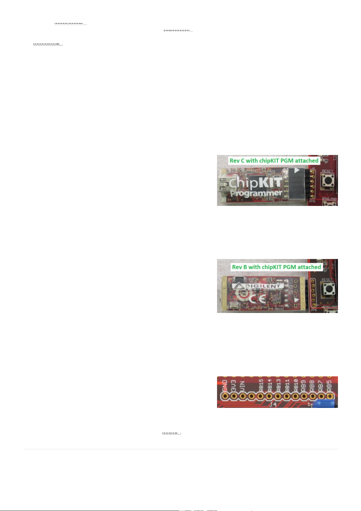
1. J3 – Digital and Analog I/O Connector #2
The set of Digital I/Os with chipKIT numbers 9 through 18 and Analog pins
A3-A8. The holes are slightly offset to allow for friction fitting of headers. See
the Pinout Diagram and Pinout Table for more details.
Rev C change: The silk screen on Rev B (image →) shows the port assignments
as used with MPLAB, not the MPIDE pin assignments. Also, the holes are not
offset, requiring headers to be soldered to the board.
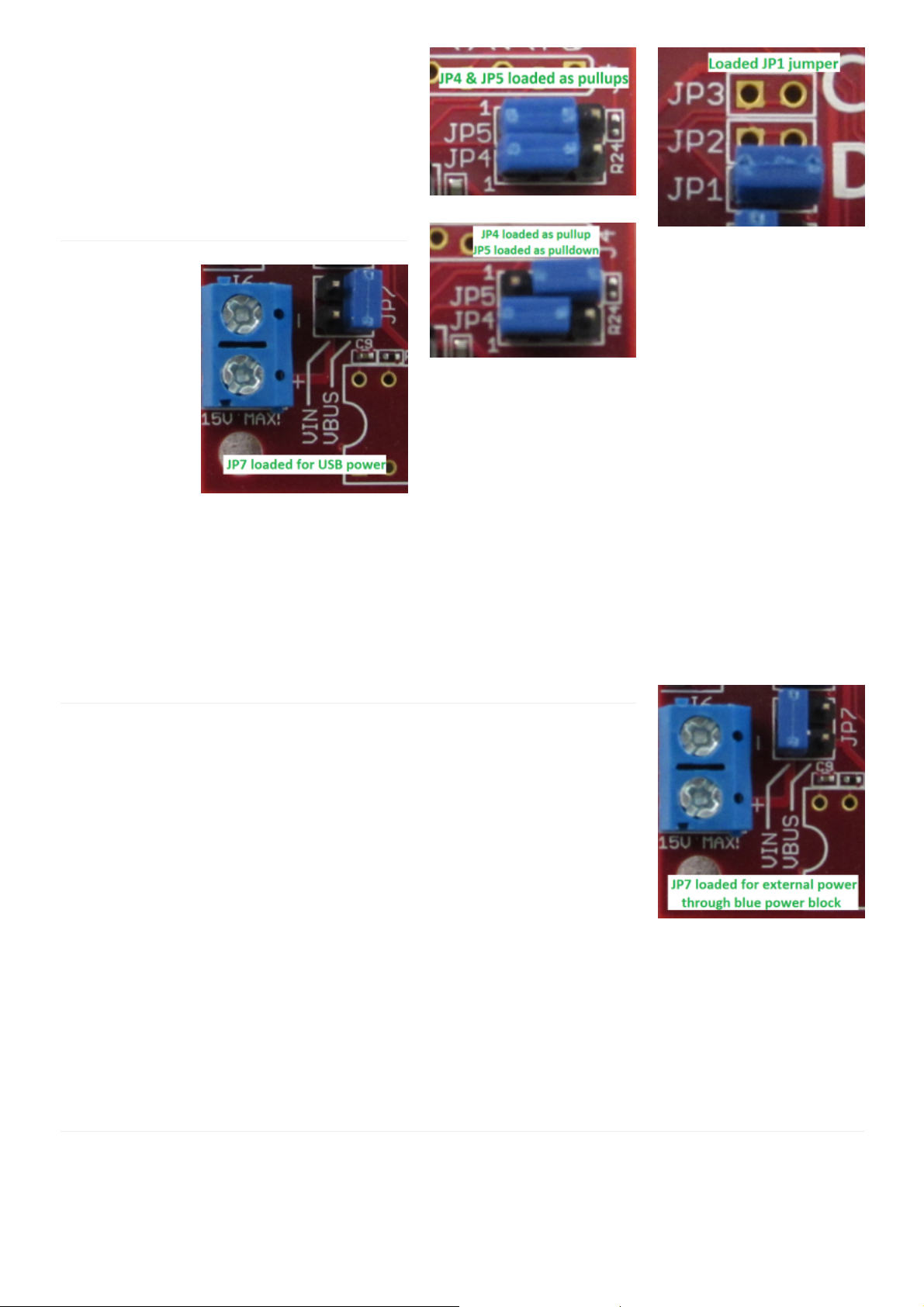
2. JP1, JP2 & JP3
JP1 – USBID Jumper for use with USB OTG:
This jumper allows Digital I/O pin 0 (RB5) to be disconnected from the USBID line on the USB Port. If JP1 is shorted, pin 0 may not
operate as expected. Some users may wish to keep JP1 shorted for USB operations.
JP2 and JP3 – D+ and D- USB Signals:
These jumpers are shipped unloaded. The trace between the two terminals may be cut if USB functionality is required to be permanently
disabled. Once the traces have been cut, it is possible to solder jumper pins in these locations to re-enable the D+ and D- signals as
desired.
3. J2 – USB Connector for USB Serial Converter
This connects to a USB port on the PC to provide the communications port for the MPIDE to talk to the DP32 board. This can also be
used to power the DP32 when connected to the PC.
4. J6 – External Power Screw Terminal Connectors
This screw terminal connector may be used to provide up to 15VDC to the DP32. The polarity of the terminals is marked on the
silkscreen and must be followed to avoid damaging the board.
5. JP7 – Power Select Jumper
This jumper may be set to either power the DP32 via USB (J2), or Screw Terminal (J6). To power via USB, set the jumper to short the
pins with VIN and VUSB directly to their right. To power via external supply, short the two pins nearest the screw terminal.
https://reference.digilentinc.com/chipkit_dp32/refmanual 3/17
Page 4
12/21/2018 chipKIT DP32 Reference Manual [Reference.Digilentinc]
6. IC4 – SPI EEPROM () Device (Microchip 25LC256) Loading Point
This 8-pin DIP footprint is designed so that a SPI controlled EEPROM () device could be added at a later time if desired. It is intended
that an 8-pin DIP socket or a Microchip 25LC256 device would be soldered into this location. The SPI signals for communicating with
this EEPROM () device are tied directly to SPI 2 on the PIC32.
7. VR1 – Analog Potentiometer
An analog potentiometer connected to chipKIT analog pin A2. When rotated fully counter clockwise, 0V is read on the pin. When
rotated fully clockwise, 3.3V is read on the pin.
8. IC3 – Analog Temperature Sensor (Microchip MCP9701A) Loading Point
This 3-pin footprint is intended for an analog temperature sensor to be loaded by the user. It was designed with the Microchip
MCP9701A Linear Active Thermistor in mind. Pin one (square pad) is for VCC3V3 of the device, pin two (center pin) is for the VOUT
pin of the device, and pin three is for the ground pin.
9. User LEDs
Four LEDs connected to digital signal pins 11, 12, 13, and 14. These LEDs are labeled as PIN_LED1, PIN_LED2, PIN_LED3, and
PIN_LED4 respectively in MPIDE.
10. IC1 PIC32 Microcontroller
The PIC32MX250F128B microcontroller is the main processor for the board.
11. JP6 – Microchip Debug Tool Connector
This connector is used to connect Microchip and Digilent
programmer/debugger tools, such as the PICkit™3 or Digilent chipKIT PGM.
This allows the DP32 board to be used as a traditional microcontroller
development board using the Microchip MPLAB® IDE. Note that the square
pad is pin 1.
Rev C change: This header is reversed from Rev B. When attaching the
debugger tool, it would appear right-side up when attached to Rev C, and upside down when attached to Rev B (see images). Be sure you know which Rev
you have. The square solder pad should connect to pin 1 on the debugger. Attaching the debugger incorrectly will almost certainly fry
either the DP32, the debugger, or both. Please refer to the section titled “Programming the DP32” of this manual for more information
on using a debugger.
12. Reset Button
When pressed, the microcontroller resets the currently loaded sketch. If Button
2 (BTN2/PGM) is held down while pressing the reset button, the
microcontroller will start from the boot loader, allowing a new sketch to be
loaded.
13. BTN2/PGM and BTN3 User Buttons
These user buttons are connected to digital signal pins 1 and 17. They produce a
logic high signal when depressed, and a logic low signal when released. When
using MPIDE, these buttons are defined in the core files as PIN_BTN_1 and PIN_BTN_2 respectively.
14. JP4/JP5 – Pullup/Pulldown jumpers
These jumpers are used to add pullups or pulldowns to the digital signal pins 2 and 3. Pullups are necessary when utilizing I2C on these
two pins. These two jumpers can be used as settable logic states either pulled high or pulled low depending on the jumper settings. In
addition, if no pullups or pulldowns are desired, the jumper may be safely removed completely, allowing the pins to be used for other
input/output purposes.
15. J4 – Digital and Analog I/O Connector #1
The set of Digital I/Os with chipKIT numbers 0 through 8 and Analog pins
A0-A2. See Pinout Diagram and Pinout Table for more details.
Rev C change: The silk screen on Rev B (image →) shows the port assignments
on the chip, not the MPIDE pin assignments. Also, the holes are not offset,
requiring headers to be soldered to the board.
16. Prototyping Area
The prototyping area has 288 through holes, broken into two main sections. One section has 28 3-hole busses. Between the 3-hole
busses are two 14-hole busses. There are also a 3V3 bus and GND () bus, each with 8 holes. The remaining 160 holes are isolated for
mounting whatever will fit using standard solder or wire wrapping methods.
https://reference.digilentinc.com/chipkit_dp32/refmanual 4/17
Page 5
12/21/2018 chipKIT DP32 Reference Manual [Reference.Digilentinc]
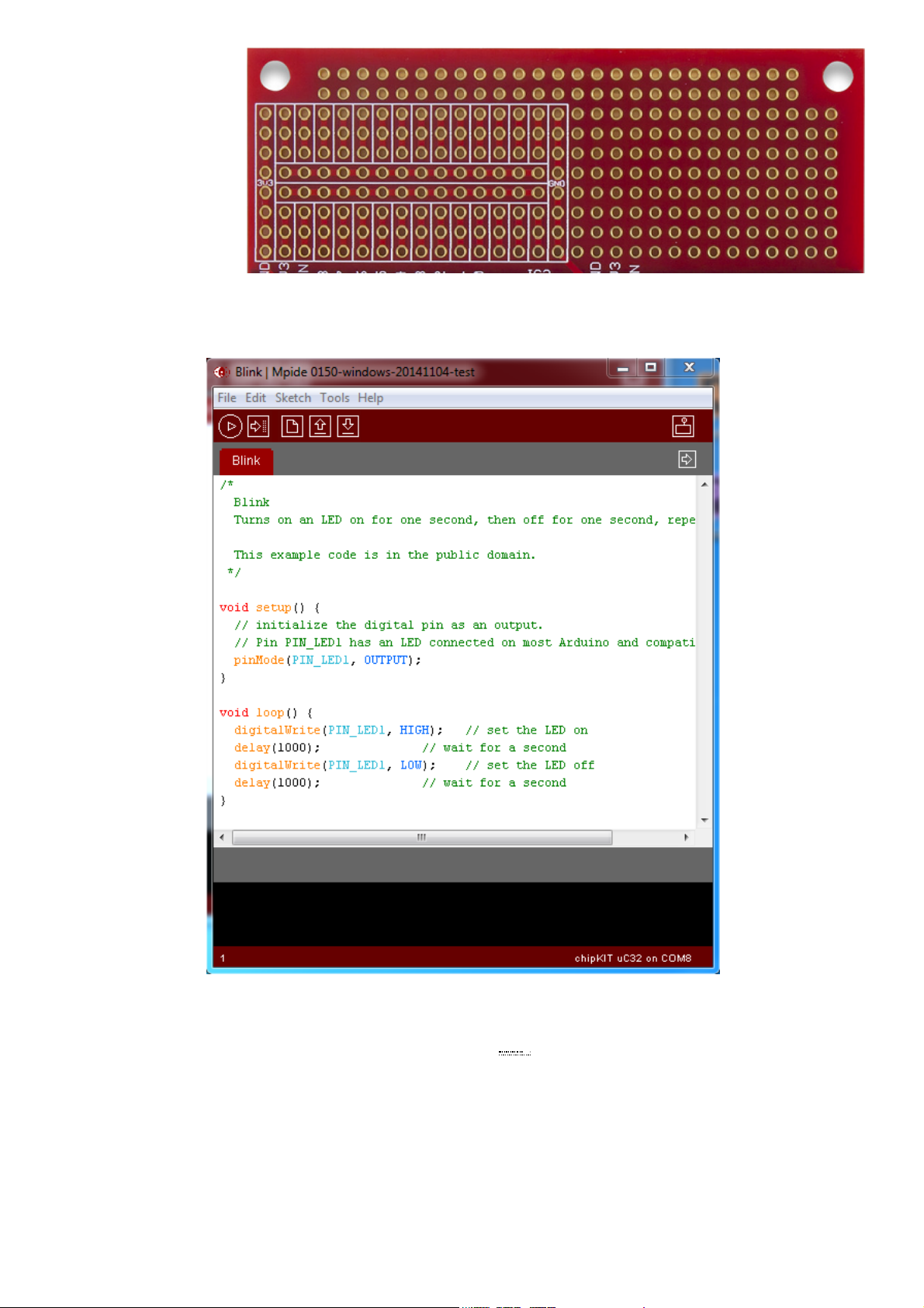
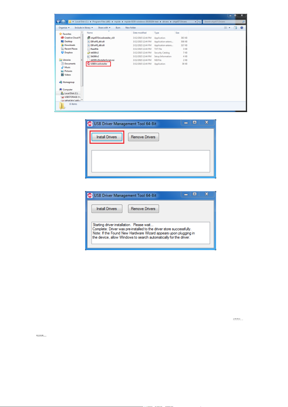
The DP32 uses the PIC32MX250F128B onboard USB peripheral to program the microcontroller with the MPIDE environment. This
requires a driver to be installed to accommodate this programing solution. The driver file is called Stk500v2.inf and is available in the
drivers folder in the MPIDE distribution. In order to install the driver on a Windows based machine, follow the steps below. You should
not need to manually install the drivers on a machine with a non-Windows OS ().
1. Open MPIDE to ensure that it works. Close it and make sure that your DP32 is unplugged from the computer.
2. Navigate to the MPIDE installation folder. The file path should be something like “C:\Program Files (x86)\mpide\mpide-0023windows-20140821\drivers\chipKIT Drivers”
3. You should see USBDriverInstaller at the bottom of the list.
3 Programming the chipKIT DP32
3.1 MPIDE Development Tool
https://reference.digilentinc.com/chipkit_dp32/refmanual 5/17
Page 6
12/21/2018 chipKIT DP32 Reference Manual [Reference.Digilentinc]
4. Open that application and click “Install Drivers”. You may need to allow admin permission for it to complete.
5. Once the drivers are installed, close the windows. Open MPIDE, connect the board with the USB cable, and allow Windows to
find and install the correct drivers.
Once the driver is installed and the computer has recognized the board, it is ready to be programmed. The board has two modes of
operation. The first is the bootloader mode, to enter this mode you must press and hold down BTN2/PGM button while pressing the
RESET button then release both to set the board into program mode. In program mode LD1 will flash to show you that the bootloader
is running and the board is ready to be programmed.
Once the board is programmed it will be reset and will execute the programmed sketch. If there is a sketch loaded on the board and you
cycle power to the board, it will automatically reenter sketch mode. Each time you edit your sketch and need to reload it to the board,
you will need to exit sketch mode by pressing and holding BTN/PGM, pressing RESET, and then releasing both to re-enter program
mode.
Since the board resets between program mode and sketch mode the serial port will disconnect and then reconnect. The MPIDE serial
monitor will not work unless there is a delay of at least 5 seconds in the user sketch before it begins to send data to the computer. To
ensure the serial monitor is ready it is recommended that users watch the device manager or similar program for your OS () after the reset
to watch for the reconnection of the serial port before attempting to open the Serial Monitor in MPIDE. The delay is required for proper
operation of the serial port so that the board can disconnect and reconnect to the computer before the DP32 begins sending data out
while the OS () is not listening. This is a byproduct of the embedded USB controller solution on the DP32.
3.2 Microchip MPLAB IDE Development Tool Campatibility
https://reference.digilentinc.com/chipkit_dp32/refmanual 6/17
Page 7

12/21/2018 chipKIT DP32 Reference Manual [Reference.Digilentinc]
In addition to being compatible with the MPIDE, the DP32 board can be used as a more traditional microcontroller development board
using Microchip Development Tools.
The unloaded connector JP6 on the right side of the board is used to connect to a Microchip development tool, such as the PICkit3™ or
the Digilent chipKIT PGM. The holes for JP6 are staggered so that a standard 100-mil spaced 6-pin header can be press fit to the board
without the need to solder it in place. Any Microchip development tool that supports the PIC32MX2xx microcontroller family and can
be used provided it uses the same 6-pin interface as the PICkit3.
The Microchip MPLAB® IDE or the MPLAB® X IDE can be used to program and debug code running on the DP32 board. These
tools can be downloaded from the Microchip website.
Using the Microchip development tools to program the DP32 board will cause the boot loader to be erased. To use the board with the
MPIDE again, it is necessary to program the boot loader back onto the board. The boot loader image can be downloaded here
(https://reference.digilentinc.com/_media/chipkit_dp32/chipkit_bootloader_dp32.zip) from the DP32 product page on the Digilent website. To
reload the boot loader, you will need to have MPLAB X and a licensed Microchip debugger/programmer, such as a PICkit®3 or
chipKIT PGM programmer, and then perform the following steps.
1. Open MPLAB X. On the top task bar, click on “File”, highlight “Import”, and click on “HEX/ELF Prebuilt File”
2. Click on “Browse” and search for the chipKIT-DP32.HEX file you downloaded from the webpage. (If you have more than one
board from the chipKIT family, it may be helpful to store all of your applicable boot loaders in one common file.)
3. Select “32-bit MCUs (PIC32)” in the “Family:” dialog box.
4. Select the device ID “PIC32MX250F128B” in the “Device:” dialog box.
5. Make sure your programmer device is connected and selected in the “Hardware Tool” box at the bottom. The chipKIT PGM was
used for this example. Click “Next” when the correct options have all been chosen.
3.3 Reloading the MPIDE Boot Loader
https://reference.digilentinc.com/chipkit_dp32/refmanual 7/17
Page 8

12/21/2018 chipKIT DP32 Reference Manual [Reference.Digilentinc]
6. Name the project whatever you wish, then click “Browse” to store it in whichever file you wish. Default names will be autopopulated.
7. Check the box labeled “Set as main project”, then click “Finish”
8. The project may not default to the main project, even if you selected it before. If it is not in bold in the project list on the left,
right click on the boot loader project, scroll down to and click on “Set As Main Project”. This should change the typeface to bold.
https://reference.digilentinc.com/chipkit_dp32/refmanual 8/17
Page 9

12/21/2018 chipKIT DP32 Reference Manual [Reference.Digilentinc]
9. Double check your board Rev, and then connect your programmer to the DP32 as indicated in point 11. in the section “chipKIT
DP32 Hardware Overview” above. At least one board LED () should light up.
10. Press and hold BTN2/PGM on the DP32, then at the top of the MPLAB window, click on the icon with a green arrow pointing
down. A dialog box titled “Licensed Debugger” will open at the bottom of the window and indicate the programming status.
Hold BTN2/PGM until it says “Programming/Verify complete”. LED1 should blink rapidly, indicating that the boot loader
install was successful and it is now in program mode and ready to be programmed with MPIDE.
A unique feature of the DP32 from the rest of the Digilent line of chipKIT boards is that the PIC32 microcontroller installed on the
board is a removable, 28-pin DIP IC. This allows for lots of flexibility in building embedded projects since you can program the IC with
the board, remove it, and then embed it into a stand-alone application without the need to purchase an additional board (additional
circuitry is required to embed the IC into stand alone projects). Additional ICs can then be acquired through Microchip directly. Simply
go to www.microchipdirect.com (https://www.microchipdirect.com/) and search for “MX250F128B”. As of this writing, there are two
options for the IC in the DIP footprint, one that comes pre-loaded with the chipKIT boot loader and one that does not.
Once you have your new ICs, the original IC can be carefully removed from the socket and the new IC installed on the DP32 board. The
new IC can now be programmed with MPLAB tools or MPIDE as described above. If you purchased the IC with the pre-loaded boot
loader, you may use either programming environment right away. If you program the IC with MPLAB first, or purchased the IC without
the chipKIT boot loader installed, you will need to use MPLAB X to load the boot loader as outlined above if you wish to use MPIDE.
JP1 USBID Connect (USB OTG)
Loaded: USBID is connected to Digital I/O pin 0 (RB5) and is usable by the microcontroller.
Unloaded: Pin 0 is unconnected to USBID and freely usable.
JP2 USB Data+
JP3 USB Data-
For most users, the traces for JP2 and JP3 should be left uncut. Cutting the trace will remove the ability to program the microcontroller
from the USB Port. Users may optionally add jumper pins and a shorting block to restore the original functionality of the DP32 if the
traces have been cut.
3.4 Programming Additional ICs
4 chipKIT DP32 Jumper Settings
https://reference.digilentinc.com/chipkit_dp32/refmanual 9/17
Page 10
12/21/2018 chipKIT DP32 Reference Manual [Reference.Digilentinc]
JP4/JP5 pullups/pulldowns
Default configuration is with the shorting blocks loaded on
pins 1 and 2, which results in pullup configuration.
Shorting pins 2 and 3 results in pulldown operation. Users
may choose to remove shorting blocks entirely if no
pullup/pulldown settings are desired.
JP7 Power Select
Jumper
Default power
select is with the
shorting block
connecting the two
pins directly next to
VBUS, providing
power from the
USB connector. If
external power is
desired, connect the
two pins nearest the
external power
screw terminal labeled VIN.
The DP32 is designed to be powered either via USB or from an external power supply. Only one supply should be selected at a time.
The DP32 has a single voltage regulator mounted on the underside which regulates either 5V from USB to 3.3V, or a maximum of 15V
external voltage to 3.3V. The 3.3V regulator is a Microchip MCP1703. This regulator is rated for a maximum output current of 250mA.
This regulator has internal short circuit protection and thermal protection. It will get noticeably warm when the current consumed by the
VCC3V3 bus is close to the 250mA maximum.
The internal USB circuit on the PIC32MX250F128B requires 5VDC to operate. Do not attempt to power the USB circuitry with the
external power screw terminal, unless it is a regulated 5V external power supply.
The PIC32 microcontroller operates at 3.3V. There are two issues to consider when dealing with 5V compatibility for 3.3V logic. The
first is protection of 3.3V inputs from damage caused by 5V signals. The second is whether the 3.3V output is high enough to be
recognized as a logic high value by a 5V input.
5 Power Supply
6 5V Compatibility
https://reference.digilentinc.com/chipkit_dp32/refmanual 10/17
Page 11

12/21/2018 chipKIT DP32 Reference Manual [Reference.Digilentinc]
Only MIPDE pin numbers 0 - 3 on the PIC32 microcontroller are 5V tolerant. All other pins are 3.3V tolerant only. To provide 5V
tolerance on those pins, you will have to add clamping diodes and current limiting resistors to those pins. Please check the Pinout
Diagram or Pinout Table to confirm 5V tolerant pins.
The minimum high-voltage output of the PIC32 microcontroller is rated at 2.4V when sourcing 12mA of current. When driving a high
impedance input (typical of CMOS logic) the output high voltage will typically be close to 3.3V. Some 5V devices will recognize this
voltage as a logic high input, and some will not you will have to read the datasheet for the 5V parts you are using to ensure that 3.3V will
satisfy the logic high conditions for the part. Many 5V logic devices will work reliably with 3.3V inputs.
The DP32 board provides all 19 I/O pins of the PIC32MX250F128B microcontroller to through-hole points on the PCB.
The PIC32 microcontroller can source or sink a maximum of 7mA on all digital I/O pins. The maximum current that can be sourced or
sunk across all I/O pins simultaneously is +/- 200mA. For more detailed specifications, refer to the PIC32MX1XX/2XX Data Sheet
available from the Microchip web site.
The DP32 uses logical pin numbers to identify digital I/O pins. Pins 0 through 8 are located on J4, counting up from the square pad of
J4. Pins 9 through 18 are located on J3, counting up from the square pad. In addition, several of these I/O pins share functionality with
other devices on the board. See the Pinout Diagram and Pinout Table for more information.
Pins 15 and 16 are shared with the crystal for the internal oscillator, and are not typically usable. Pin 6 is shared with the Analog
Temperature Sensor. Pin 8 is shared with the onboard Potentiometer. Pins 4 and 5 are shared with the USB Data+ and Data- signals. Pin
0 is shared with the USBID function, but removing jumper 1 clears this conflict. Pins 9, 18, 7, and 10 are used for the SPI EEPROM ()
device if it is loaded, on its Chip Select, Master Out/Slave In, Serial Clock, and Master In/Slave Out lines respectively.
In addition to the digital I/O, there are Analog inputs available on the board, called A0 through A8. These pins are shared on digital pins
6 thru 14.
I C
Synchronous serial interface. The I C1 interface is available on pins 2 and 3. When using the I C interface, it is necessary to set JP4 and
JP5 such that pullups are present on the bus. This is done by moving the jumper blocks to pins 2 and 3 on each jumper.
User LEDs
Pins 11 (LD4), 12 (LD3), 13 (LD2) and 14 (LD1) are shared between the through-hole connection and the LED (). Driving the pin high
turns the LED () on, driving it low turns it off.
User Buttons
Pins 1 (BTN3) and 17 (BTN2/PGM) are shared between a through-hole connection and a push button. Pushing the button drives the
input high. Releasing it brings the input low.
External Interrupts
Only INT0 is hard-mapped on the microcontroller. It is connected to pin 1. The other external interrupts are accessible via PPS
described below.
Reset
The Reset button is utilized to bring the MCLR pin low on the microcontroller, thus restarting the currently loaded sketch. If the user
wishes to reprogram the device, it is necessary to first hold down BTN2/PGM, and then press the reset button. This forces the
microcontroller to default to the boot loader.
An advanced feature of the PIC32MX1xx/2xx families of microcontrollers is the ability to re-map the locations of peripheral devices.
This advanced feature is available only if you are using Microchip's MPLAB® programming tools. The PPS Assigned Peripheral options
are:
Output Compare
Pin 8 (OC1), Pin 2 (OC2), Pin 3 (OC3), Pin 13 (OC4), Pin 6 (OC5). Output compare allows for the implementation of PWM signals.
Input Capture
Pin 6 (IC1), Pin 11 (IC2), Pin 2 (IC3), Pin 14 (IC4), Pin 13 (IC5). Input capture allows for the synchronization of timers with captured
signals, along with the execution of interrupts.
External Timer Input
Pin 18 (TCK1), Pin 14 (TCK2), Pin 12 (TCK3), Pin 6 (TCK4), Pin 3 (TCK5) allows for timers to be clocked from external sources.
External Interrupt
Pin 3 (INT1 ()), Pin 13 (INT2 ()), Pin 2 (INT3 ()), Pin 17 (INT4) allows for external interrupts to be triggered in their own ISRs.
Interrupts may be edge triggered or level triggered, though only one of rising, falling, high, or low, may be chosen for trigger sensitivity.
7 Input/Output Connections
8 Peripheral I/O Functions
2
2 2
8.1 Peripheral Pin Select
https://reference.digilentinc.com/chipkit_dp32/refmanual 11/17
Page 12

12/21/2018 chipKIT DP32 Reference Manual [Reference.Digilentinc]
Change Notice Pins
All change notice pins are matched with their chipKIT pin numbers (e.g. CN0 is associated with Pin 0). There is a change notice pin for
each I/O pin.
UART
Pin 14 (U1TX), Pin 6 (U1RX), Pin 7 (U2TX) and Pin 10 (U2RX) are used to implement UART peripheral controls. Unlike other
chipKIT boards, the USB Serial communication is not implemented using a UART controller.
SPI
Synchronous serial port. Pin 9 (SS), Pin 18 (MOSI ()), Pin 7 (SCK), Pin 10 (MISO ()). This uses SPI1 on the PIC32 Microcontroller. The
second SPI is implemented as Pin 14 (SS), Pin 2 (MOSI ()), Pin 13 (MISO ()), and Pin 8 (SCK).
This pin map does not define the full functionality for every pin. For a complete reference of pin functionality, please see the
PIC32250F128B datasheet available from Microchip. http://ww1.microchip.com/downloads/en/DeviceDoc/60001168F.pdf
(http://ww1.microchip.com/downloads/en/DeviceDoc/60001168F.pdf)
When using TimerSerial (UART) ports with MPIDE HardwareSerial library, object “Serial” uses TX1/RX1, and object “Serial1” uses
TX2/RX2.
chipKIT Pin#PIC32
Pin
register
ID PIC32 Signal Notes
0* 14 RB5 TMS/RPB5/USBID USBID w/ JP1
loaded
1* 16 RB7 TDI/RB7/CTED3/PMD5/INT0 BTN3 ‡
2* 17 RB8 TCK/RPB8/SCL1/CTED10/PMD4 PU/PD w/ JP5
3* 18 RB9 TDO/RPB9/SDA1/SCTED4/PMD3 PU/PD w/ JP6
4 21 RB10 PGED2/RPB10/D+/CTED11 USB Data+
Appendix A: Pinout Diagram
Appendix B: Pinout Table by chipKIT Pin Number
https://reference.digilentinc.com/chipkit_dp32/refmanual 12/17
Page 13

12/21/2018 chipKIT DP32 Reference Manual [Reference.Digilentinc]
chipKIT Pin#PIC32
Pin
register
ID PIC32 Signal Notes
5 22 RB11 PGEC2/RPB11/D- USB Data-
6/A0 24 RB13 AN11/RPB13/CTPLS/PMRD Analog Temp
Pin
7/A1 25 RB14 CVREF/AN10/C3INB/RPB14/VBUSON/SCK1/CTED5 IC4 – Serial
Clock
8/A2 26 RB15 AN9/C3INA/RPB15/SCK2/CTED6/PMCS1 Dial Pot – Pin
A2
9/A3 2 RA0 PGED3/VREF+/CVREF+/AN0/C3INC/RPA0/CTED1/PMD7 IC4 – Chip
Select
10/A4 3 RA1 PGEC3/VREF-/CVREF-/AN1/RPA1/CTED2/PMD6 IC4 – Serial Out
11/A5 4 RB0 PGED1/AN2/C1IND/C2INB/C3IND/RPB0/PMD0 LD4 ¤
12/A6 5 RB1 PGEC1/AN3/C1INC/C2INA/RPB1/CTED12/PMD1 LD3 ¤
13/A7 6 RB2 AN4/C1INB/C2IND/RPB2/SDA2/CTED13/PMD2 LD2 ¤
14/A8 7 RB3 AN5/C1INA/C2INC/RTCC ()/RPB3/SCL2/PMWR LD1 ¤
15 9 RA2 OSC1/CLKI/RPA2 8 MHz () Clock
In
16 10 RA3 OSC2/CLKO/RPA3/PMA0 8 MHz () Clock
Out
17 11 RB4 SOSCI/RPB4 BTN2/PGM ‡
18 12 RA4 SOSCO/RPA4/T1CK/CTED9/PMA1 IC4 – Serial In
- 1* - nMCLR -
- 8 - GND () -
- 13 - VDD -
- 15* - VBUS -
- 19 - GND () -
- 20 - VCAP -
- 23 - VUSB3V3 -
- 27 - AVSS N/C
- 28 - AVDD -
* Indicates 5V tolerant I/O pin
‡ When using MPIDE, there are macros defined for BTN2/PGM (PIN_BTN1) and for BTN3 (PIN_BTN2). You may also use the
chipKIT pin # if you wish (#17 for BTN2/PGM, #1 for BTN3)
¤ When using MPIDE, there are macros defined for the LEDs, e.g. PIN_LED1 is assigned to LD1, PIN_LED2 to LD2, etc. You may
also use the chipKIT pin # if you wish (#14 for LD1, #13 for LD2, etc.)
https://reference.digilentinc.com/chipkit_dp32/refmanual 13/17
Page 14

12/21/2018 chipKIT DP32 Reference Manual [Reference.Digilentinc]
For a more detailed explanation of the functionality of each pin and the PIC32 architecture, please see the datasheet from Microchip.
http://ww1.microchip.com/downloads/en/DeviceDoc/60001168F.pdf
(http://ww1.microchip.com/downloads/en/DeviceDoc/60001168F.pdf)
Socket
Pin #
chipKIT
Pin #
Connector
Pin # PIC32 Signal Notes
1* - - nMCLR Reset
button
circuit
2 9/A3 RA0 PGED3/VREF+/CVREF+/AN0/C3INC/RPA0/CTED1/PMD7/RA0 IC4 –
Chip
Select
3 10/A4 RA1 PGEC3/VREF-/CVREF-/AN1/RPA1/CTED2/PMD6/RA1 IC4 –
Serial
Out
4 11/A5 RB0 PGED1/AN2/C1IND/C2INB/C3IND/RPB0/PMD0/RB0 LD4
5 12/A6 RB1 PGEC1/AND3/C1INC/C2INA/RPB1/CTED12/PMD1/RB1 LD3
6 13/A7 RB2 AN4/C1INB/C2IND/RPB2/SDA2/CTED13/PMD2/RB2 LD2
7 14/A8 RB3 AN5/C1INA/C2INC/RTCC ()/RPB3/SCL2/PMWR/RB3 LD1
8 - GND () VSS
9 15 RA2 OSC1/CLKI/RPA2/RA2 8 MHz
() Clock
In
10 16 RA3 OSC2/CLKO/RPA3/PMA0/RA3 8 MHz
() Clock
Out
11 17 RB4 SOSCI/RPB4/RB4 BTN4
12 18 RA4 SOSCO/RPA4/T1CK/CTED9/PMA1/RA4 IC4 –
Serial
In
13 - VDD VDD
14* 0 RB5 TMS/RPB5/USBID/RB5 USBID
w/ JP1
short
15* - VBUS VBUS
16* 1 RB7 TDI/RB7/CTED3/PMD5/INT0/RB7 BTN3
17* 2 RB8 TCK/RPB8/SCL1/CTED10/PMD4/RB8 PU/PD
w/ JP5
18* 3 RB9 TDO/RPB9/SDA1/SCTED4/PMD3/RB9 PU/PD
w/ JP6
Appendix C: Pinout Table by Socket Pin
https://reference.digilentinc.com/chipkit_dp32/refmanual 14/17
Page 15

12/21/2018 chipKIT DP32 Reference Manual [Reference.Digilentinc]
Socket
Pin #
chipKIT
Pin #
Connector
Pin # PIC32 Signal Notes
19 - GND () VSS
20 - - VCAP
21 4 RB10 PGED2/RPB10/D+/CTED11/RB10 USB
Data+
22 5 RB11 PGEC2/RPB11/D-/RB11 USB
Data-
23 - - VUSB3V3
24 6/A0 RB13 AN11/RPB13/CTPLS/PMRD/RB13 Analog
Temp
Pin A0
25 7/A1 RB14 CVREF/AN10/C3INB/RPB14/VBUSON/SCK1/CTED5/RB14 IC4 –
Serial
Clock
26 8/A2 RB15 AN9/C3INA/RPB15/SCK2/CTED6/PMCS1/RB15 Dial
Pot –
Pin A2
27 - - AVSS N/C
28 - - AVDD
* Pins are 5V tolerant
The schematic is available as a PDF download (https://reference.digilentinc.com/_media/chipkit_dp32/chipkit_dp32_sch.pdf) from the DP32
product page on the Digilent website.
Appendix D: Schematic
First Name
Last Name
Email Address
Submit
Subscribe to our Newsletter
Xilinx University
Program
(https://store.digilentinc.com/partners/xilinxuniversity-program/)
Technology Partners
(https://store.digilentinc.com/technologypartners/)
Distributors
(https://store.digilentinc.com/our-
Our Partners
Technical Support
Forum
(https://forum.digilentinc.com)
Reference Wiki
(https://reference.digilentinc.com)
Contact Us
(https://store.digilentinc.com/contactus/)
Help
Videos
(https://youtube.com/user/digilentinc)
FAQ
(https://resource.digilentinc.com/verify/faq)
Store Info
(https://store.digilentinc.com/storeinfo/)
Customer Info
About Us
(https://store.digilentinc.com/
pageid=26)
Shipping & Returns
(https://store.digilentinc.com/
returns/)
Legal
(https://store.digilentinc.com/
Company Info
https://reference.digilentinc.com/chipkit_dp32/refmanual 15/17
Page 16

12/21/2018 chipKIT DP32 Reference Manual [Reference.Digilentinc]
distributors/) Jobs
(https://store.digilentinc.com/
Internships
(https://store.digilentinc.com/
(https://twitter.com/digilentinc)
(https://www.facebook.com/Digilent)
(https://www.youtube.com/user/DigilentInc)
(https://instagram.com/digilentinc)
(https://github.com/digilent)
(https://www.reddit.com/r/digilent)
(https://www.linkedin.com/company/1454013)
(https://www.flickr.com/photos/127815101@N07)
Connect With Us
https://reference.digilentinc.com/chipkit_dp32/refmanual 16/17
Page 17

12/21/2018 chipKIT DP32 Reference Manual [Reference.Digilentinc]
https://reference.digilentinc.com/chipkit_dp32/refmanual 17/17
 Loading...