

Page 1
CCeerreebboott IIII™
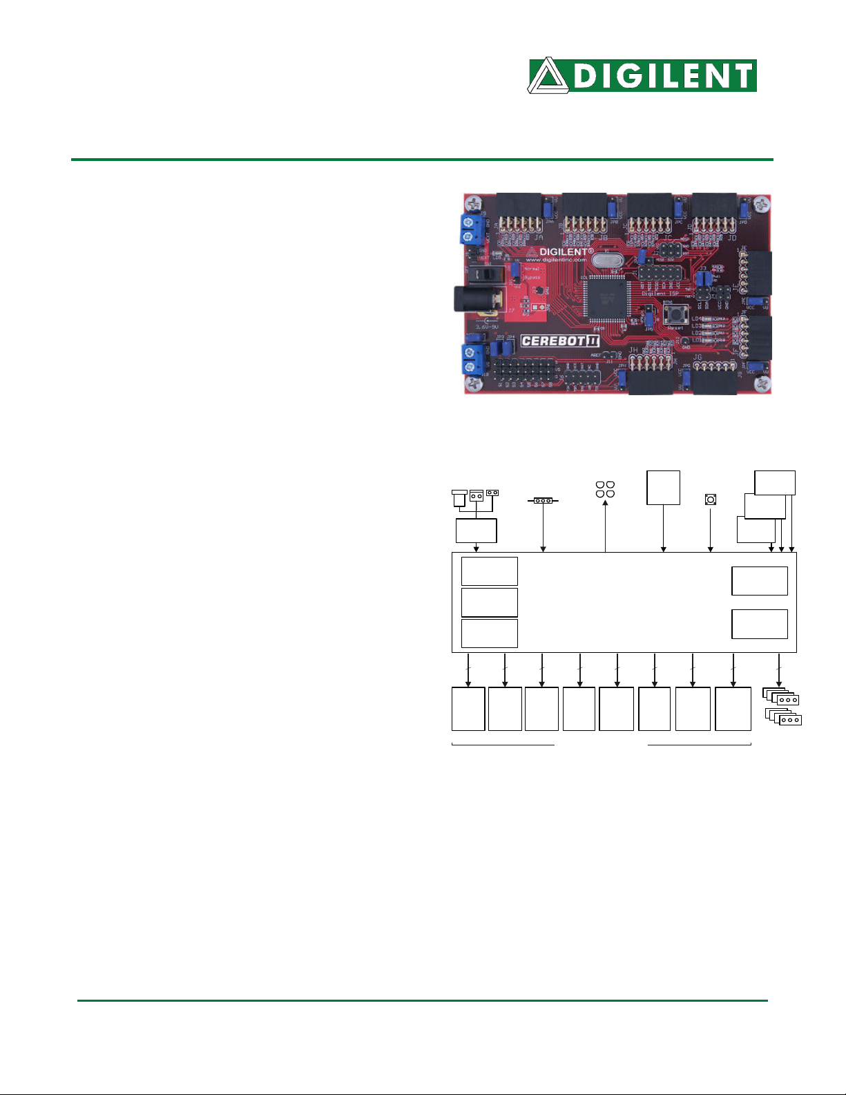
Cerebot II Circuit Diagram
RReeffeerreennccee MMaannuuaal
™ BBooaarrdd
l
Revision: February 9, 2009
Note: This document applies to REV B of the board.
Overview
The Cerebot II board is a useful tool for
embedded control and robotics projects for
both students and hobbyists.
Its versatile design and programmable
microcontroller lets you access numerous
peripheral devices and program the board for
multiple uses. The board has many I/O
connectors and power supply options and
supports a number of programming options
including the free Atmel AVR® Studio 4, and
WinAVR.
The Cerebot II has a number of connections
for peripheral devices. It provides eight
connectors for attaching Digilent Pmod™
peripheral modules. Digilent peripheral
modules include H-bridges, analog-to-digital
and digital-to-analog converters, speaker
amplifier, switches, buttons, LEDs, as well as
converters for easy connection to RS232,
screw terminals, BNC jacks, servo motors, and
more.
Features include:
• an ATmega64L microcontroller
• eight hobby RC servo connectors
• eight Pmod connectors for Digilent
peripheral module boards
• an on-board voltage regulator
• multiple flexible power supply jumper
options
• support for the Digilent JTAG-3 Parallel
and JTAG-USB programming cables
• support for the Atmel AVRISP insystem programmer
• support for the Atmel AVR JTAGICE
mkII debugging tool
• ESD protection and short circuit
protection for all I/O pins.
Various po wer
conn ectors
3.3V
regu lator
64K Flash
(Inte rnal)
2K E EPRO M
(Inte rnal)
4K S RAM
(Inte rnal)
8
JA
Mem
Mem
Adr/
Data
www.di g i l e n t i n c . com
215 E Main Suite D | Pullman, WA 99163
User Input
Jumper
VCC
(509) 334 6306 Voice and Fax
4 LE Ds
GND
8MH z
crys tal
Reset
button
Atmel
ICE port
Inter nal
Oscillator
Atmel
ISP port
ATmega64L
TQ6 4
8 8 8 4 4 4 8
JB
JC
JD
Adr
Mem
SPI
Ctl
UAR T
TWI
UAR T
Eight Pmod conne ctors
JE
H-bri dgeJFH-br idge
LED s
JG
H-bri dge
&
UART, SPI,
&TW I port s
8
JH
Anal og
&
JTA G
®
Digil ent
ISP port
Eigh t servo
conn ectors
Doc: 502-128 page 1 of 10
Copyright Digilent, Inc. All rights reserved. Other product and company names mentioned may be trademarks of their respective owners.
Page 2

Cerebot II Reference Manual Digilent, Inc.
Features of the ATmega64L include:
• a serial peripheral interface (SPI)
• two USART serial interfaces
• Atmel TWI serial interface
• eight 10-bit analog inputs
• two 8-bit timer counters
• two 16-bit timer counters
• 64KB program flash
• 2KB user EEPROM
• 4KB internal RAM
• an analog comparator.
For more information on the ATmega64L
microcontroller, refer to the data sheet
available at www.atmel.com.
Functional Description
The Cerebot II is designed for embedded
control and robotic applications as well as
microprocessor experimentation. Firmware
suitable for many applications can be
downloaded to the Cerebot II’s programmable
ATmega64L microcontroller.
The board has a number of connection
options, and is specially designed to work with
the Digilent line of Pmod peripheral modules
with various input and output functions. For
more information, see www.digilentinc.com.
The Cerebot II has two programming interface
options: The Digilent in-system-programming
option is accessed via connector J1. A Digilent
USB or parallel programming cable can be
attached to connector J1. The Digilent AVR
Programmer application, available from the
Digilent Web site, can be used to program the
board via the Digilent programming cable.
Alternatively, the Atmel AVRISP in-system
programmer can be used. The AVRISP is
connected to connector J2 and programming is
done using the Atmel in-system-programming
application built into the Atmel AVR Studio
software. The Cerebot II also provides the
ability to use the Atmel AVR JTAGICE mkII
debugging tool for programming the board and
debugging the user firmware.
www.digilentinc.com page 2 of 10
Copyright Digilent, Inc. All rights reserved. Other product and company names mentioned may be trademarks of their respective owners.
The Cerebot II features a flexible power supply
routing system with a number of options for
powering the Cerebot II as well as peripheral
modules connected to the board.
Pmod Connectors
The Cerebot II has eight Pmod connectors for
connecting to Digilent Pmod peripheral
modules. There are two styles of Pmod
connector. The original Pmod connector
standard uses a six-pin-header style of
connectors providing four I/O signals, ground
and a switchable power connection. The power
connection is switchable between the
regulated 3.3V main board supply and the
unregulated input supply.
The newer Pmod connector standard uses a
12-pin (2x6) header connector and provides
eight signal pins, two grounds, and two
switchable power connections. The pin
arrangement is such that the new connector is
equivalent to two of the older connectors.
Digilent Pmod peripheral modules can either
be plugged directly into the connectors on the
Cerebot II or attached via cables. Digilent has
a variety of Pmod interconnect cables
available.
See the “Pmod Headers and SPI Connection”
section below for more information about
connecting peripheral modules and other
devices to the Cerebot II. It lists the header
connectors with their designed base function
and a mapping to the Atmega64L I/O register
ports. All pins can be used as general-purpose
digital I/O ports.
Power Supply Connectors
The Cerebot II may be powered via dedicated
power supply connectors, or it can be powered
through any of the board’s Pmod connectors.
The Cerebot II can also be powered through
the servo power connector.
The Cerebot II is rated for external power from
3.6 to 9 volts DC. Using voltage outside this
Page 3

Cerebot II Reference Manual Digilent, Inc.
range could damage the Cerebot II and
connected devices.
There are three different power supply
connectors on Cerebot II for board/processor
power: J7, J8, and J9.
The barrel connector, J7, is useful for desktop
development and testing where use of
batteries is cost- or time-prohibitive. J7 is the
connector used by the AC supply adapter
available from Digilent. J7 is a 2.5mm x 5.5mm
coaxial connector wired with the center
terminal as the positive voltage.
J8 is a two-pin male header that provides easy
battery or battery-pack connection. Digilent has
both two-cell and four-cell AA battery holders
with two pin connectors available for
connection to J8.
J9 is a screw terminal connector for an
alternative power supply connection.
Connectors J7, J8, and J9 are wired in parallel
and connect to one terminal of the power
switch, SW1. The other terminal of SW1
connects to the main unregulated power bus
VU. The VU power bus connects to the center
terminal of the voltage regulator input jumper
JP1 and also connects to the VU terminal of
the power select jumper associated with each
Pmod connector.
Jumper JP1 is used to select the voltage for
the main board power bus VCC. When JP1 is
in the ‘normal’ position, the VCC power bus is
powered by the output of the on-board 3.3V
regulator. When JP1 is in the ‘bypass’ position,
the on-board voltage regulator is bypassed and
the VCC bus is connected directly to the VU
bus. In this case, the microcontroller and other
on-board electronics are powered directly from
the voltage supply connected to VU. In this
case, the input voltage must be in the range
2.7V – 5.5V. A supply voltage outside this
range can permanently damage the board.
You can also power the Cerebot II from any
Pmod header connector. Place the power
connector in the VU position to supply power to
the VU bus, or the VCC position to supply
power to the VCC bus. If power is being
supplied to the VU bus, JP1 should be in the
‘normal’ position so that the on-board regulator
will be able to regulate the supplied voltage to
the 3.3V board operating voltage. If the Pmod
connector power routing jumper is in the VCC
position, the shorting block on JP1 should be
placed in the ‘bypass’ position or removed.
The Cerebot II has a second screw terminal
connector, J10 that supplies power to the
servo power bus, VS, to power the RC hobby
servo connectors. This allows servos to be
powered from a separate power supply than
the one powering the electronics on the
Cerebot II. This can be useful when using
servos that draw large amounts of power.
Jumper JP2 can be used to connect the
Cerebot II unregulated power bus VU to the
servo power bus, VS. When no shorting block
is installed on JP2, the VU and VS busses are
separate. When a shorting block is on JP2, the
two busses are joined and the VU bus can be
powered in any of the previously indicated
ways, or from connector J10.
The Cerebot II can provide power to any
peripheral modules attached to the Pmod
connectors and to TWI devices powered from
the TWI power daisy chain connectors, J4 and
J5. Each Pmod connector provides power pins
that can be powered by either unregulated
voltage, VU, or regulated voltage, VCC, by
setting the voltage jumper block to the desired
position. The TWI power connectors only
provide regulated voltage, VCC.
The regulated voltage on the VCC bus is
provided by an on-board voltage regulator.
This regulator is capable of providing a
maximum of 500mA of current. The
ATmega64L microcontroller will use
approximately 15mA when running at 8MHz.
The remaining current is available to provide
power to attached Pmod and TWI devices. The
regulator is on the bottom of the board, near
the power connectors, and will get warm when
select jumper associated with the Pmod
www.digilentinc.com page 3 of 10
Copyright Digilent, Inc. All rights reserved. Other product and company names mentioned may be trademarks of their respective owners.
Page 4

Cerebot II Reference Manual Digilent, Inc.
the amount of current being used is close to its
limit.
Power Supply Monitor Circuit
The Cerebot II microcontroller can measure
the power supply voltage on the VU and VS
power busses using the provided power supply
monitor circuits. This feature is especially
useful when using batteries because it allows
the microcontroller firmware to determine the
charge state of the battery and potentially
notify the user when a battery supply is low.
Each power supply monitor circuit made up of
a voltage divider that divides the power bus
voltage by four, and a zener diode to clamp the
resulting voltage to no greater than 3.3V.
Jumper JP3 enables the supply monitor circuit
for VU power, and jumper JP4 enables the
supply monitor circuit for VS power. The
analog to digital converter built into the
ATmega64 is used to measure the power
supply voltages. ADC channel 0 is used to
measure VU and ADC channel 1 is used to
measure VS.
When the power supply monitor circuit is
enabled the maximum safe voltage on VU is
9V and the maximum safe voltage on VS is
12V.
RC Servo Connectors
The Cerebot II provides eight 3-pin RC hobby
servo connectors for direct control of servos in
robotics and embedded hardware actuator
applications. The connectors share I/O pins
with Pmod connector JH on the left lower side
of the Cerebot II. Individual I/O pins may be
accessed through the JH header if they're not
in use by a servo. Refer to the ATmega64
data sheet for information on how to access
the I/O pins.
RC Servos use a pulse width modulated
signal, PWM, to control the servo position. The
8-bit and 16-bit timers in the AVR
microcontroller have the ability to generate
PWM signals using the output compare
timer interrupts to accomplish this same thing.
Using timer interrupts allows a single timer
(preferably one of the 16-bit timers) to be used
to control the signal timing for all eight servo
connectors.
The servo connectors on the Cerebot II board
are intended to be driven using timer interrupts
rather than directly by the pulse width
modulators in the internal timers. This frees the
pulse width modulators for other uses, such as
DC motor speed control. Digilent has a
reference design available (the ServoMini
Reference Design) that illustrates using timer
interrupts to control signal timing for the PWM
signals to control RC servos.
The I/O pins shared between the servo
connectors and connector JH are the analog to
digital converter inputs on the ATmega64
microcontroller. If servos are being driven on
some channels and analog voltages are being
read on other pins simultaneously, it is
possible for digital switching noise to reduce
the accuracy of the analog to digital
conversions. If this is an issue, perform the
analog-to-digital conversions at times when the
servo pins are not switching. In normal
applications, there will be a great deal of dead
time when the servo pins are not switching.
There are three power options for servo
connections: a common power bus (VU) for the
Cerebot II and servos, separate on-board
power busses (VU and VS) for the Cerebot II
and servos, and an external power bus for
servos.
Install the shorting block on JP2 to connect the
VS servo power bus to the VU power bus. The
VU bus can be powered from the coax power
connector, J7, the screw terminal connector,
J9, or the 2-pin battery connector, J8.
The VU bus can also be powered from any of
the Pmod header interface connectors by
setting the corresponding power jumper block
to the VU position. This option is not suitable
for providing power for large numbers of
servos or servos that have a high current
demand.
registers. However, it is also possible to use
www.digilentinc.com page 4 of 10
Copyright Digilent, Inc. All rights reserved. Other product and company names mentioned may be trademarks of their respective owners.
Page 5

Cerebot II Reference Manual Digilent, Inc.
Remove the shorting block from jumper JP2 to
make the VS servo power bus independent
from the VU bus. In this case, the VS bus is
powered from screw terminal connector J10.
Finally, for very high current applications, a
separate power bus external to the Cerebot II
can be used to provide servo power. In this
case, remove the shorting block on JP2, tie the
external servo power bus ground to the
Cerebot II ground through the ground terminal
on J10, and use pin 1 on the servo connectors
to bring the servo control signals out to the
servos. The servo power and ground
connections are made off-board.
The on-board servo power bus can be used to
provide a maximum of 2A to each servo
connector and 5A total to all servo connectors.
Programming Options
The Cerebot II provides two in-system
programming connections, J1 and J2.
Connector J1 is the Digilent ISP connector.
This provides for in-system programming using
a Digilent parallel JTAG/SPI cable or a Digilent
USB-JTAG/SPI cable. When connecting the
Digilent JTAG/SPI cables, ensure that the VCC
and GND pin labels from the cable match to
the VCC and GND pins on the Cerebot II.
When using a Digilent programming cable, use
the Digilent AVR Programmer application
available for download from the Digilent web
site (www.digilentinc.com) to program the
board.
Connector J2 is a 6-pin (3x2) header for insystem programming using the Atmel AVRISP
(Atmel P/N ATAVRISP) programmer. When
connecting to the Cerebot II, the red indicator
line on the AVRISP connection plug must be
aligned with the top pins MISO and VCC on J2.
Programming can be accomplished using
several AVR programming applications
including the Digilent AVR Programmer
(AVRP), AVRDUDE from the WinAVR tool set,
and Atmel’s AVR Studio. Programming via
AVR Studio requires use of the Atmel AVRISP
programmer hardware. See the user’s
www.digilentinc.com page 5 of 10
Copyright Digilent, Inc. All rights reserved. Other product and company names mentioned may be trademarks of their respective owners.
documentation for each of these applications
for more information on board programming.
Debugging with the Atmel
JTAGICE mkII
Connector J6 on the Cerebot II is provided for
the Atmel JTAGICE mkII (Atmel P/N
ATJTAGICE2) in-circuit emulator for
debugging purposes. The JTAGICE works with
the debugger in Atmel’s AVR Studio product.
The JTAG port on the ATmega64 must be
enabled when using the JTAGICE. The
Cerebot II is shipped with the JTAG port
disabled. This port can be enabled or disabled
using a fuse bit which can be set with any of
the supported in-system programmers
described above.
Two Wire Serial Interface
The Atmel Two Wire Serial Interface (TWI)
provides a medium speed (400K bps)
synchronous serial communications bus. The
TWI interface provides master and slave
operation with up to 127 devices on the bus.
Each device is given a unique address, and
the protocol provides the ability to address
packets to a specific device or to broadcast
packets to all devices on the bus. See the
ATmega64 data sheet for detailed information
on configuring and using the two wire serial
interface.
The Cerebot II provides two ways to connect to
a TWI bus. The TWI signals (SCL and SDA)
are available on the connector JD (pins 7 and
8) or on the TWI daisy chain connector, J3.
Connector J3 provides two positions for
connecting to the TWI signals. By using twowire cables (available separately from Digilent)
a daisy chain of multiple Cerebot II boards or
other TWI-capable boards can be created.
The TWI bus is an open-collector bus. Devices
on the bus actively drive the signals low. The
high state on the TWI lines is achieved by pull-
Page 6

Cerebot II Reference Manual Digilent, Inc.
up resistors when no device is driving the lines
low. One device on the TWI bus must provide
the pull-up resistors. The Cerebot II board
provides pull-up resistors that can be enabled
or disabled via jumper blocks on the ‘pull-up’
positions on J3. The pull-ups are enabled by
installing jumper blocks on J3 and are disabled
by removing the jumper blocks. The shorting
blocks are placed so that they line up with the
SCL and SDA labels on the board. Only one
device on the bus should have the pull-ups
enabled.
The RC oscillator’s nominal frequency
assumes operation at 5V. The Cerebot II
normally operates at 3.3V. See the oscillator
frequency vs. supply voltage chart in the
ATmega64 data sheet to determine the
nominal frequency at 3.3V.
Although the Cerebot II will normally be
operated using the 8MHz crystal oscillator, the
internal oscillator can be selected to operate
the board at a lower frequency if desired. The
clock source to be used by the board is chosen
using the fuse settings in the in-system
programmer.
When changing the clock source fuse settings,
TWI-1
TWI-2
TWI-1
TWI-2
it is extremely important to ensure that the
clock source chosen actually exists on the
board (i.e., only choose the crystal oscillator or
SCL
SDA
Pull-ups
Enabled
Jumper Settings for TWI Pull-Up Resistors
Connectors J4 and J5 are provided for daisychaining power along with the TWI signals.
These can be use to pass power from the
Cerebot II to other devices on the TWI bus.
Either of these connectors could also be used
to provide power to the Cerebot II from some
other board on the TWI bus.
Crystal Oscillator
The ATmega64 microcontroller supports
numerous clock source options for the main
processor operating clock. The Cerebot II has
an 8MHz oscillator crystal for use with the
crystal oscillator option. The Cerebot II comes
from the factory with the external crystal
oscillator source selected.
The ATmega64 microcontroller also provides
an internal RC oscillator that can operate at
nominal frequencies of either 1MHz, 2MHz,
4MHz, or 8MHz. This internal oscillator has a
frequency variability of approximately 2-3%,
which is suitable for many applications.
SCL
Pull-ups
Disabled
SDA
internal oscillator). The ATmega64 internal insystem-programming state machine operates
from the selected clock source and if an
unavailable clock source is selected, the board
may no longer be programmable.
In some cases, it is possible to recover the
board if an improper clock source is chosen,
but not always. There is an applications note
“Cerebot Clock Source Fix” (available from
www.digilentinc.com) that explains the
procedure for recovering a board that has had
an improper clock source programmed.
User I/O Devices
The Cerebot II board has a two-position jumper
for user input and four LEDs for output. The
user input jumper, JP5, is connected to I/O port
G, bit 4. To read this jumper, bit 4 of port G
must be set as an input by clearing bit 4 in the
port G data direction register (DDRG) and
reading the pin register for port G (PING).
When the shorting block is in the ‘0’ position,
bit 4 in the pin register will be 0. When the
shorting block is in the ‘1’ position, bit 4 will be
1.
The four LEDs are connected to bits 4-7 of I/O
port E. LED 1 is connected to bit 4, LED 2 is
connected to bit 5, and so on. These four bits
are also shared with the four I/O signals on
www.digilentinc.com page 6 of 10
Copyright Digilent, Inc. All rights reserved. Other product and company names mentioned may be trademarks of their respective owners.
Page 7

Cerebot II Reference Manual Digilent, Inc.
Pmod connector JF. To use the LEDs, set the
desired bits as outputs by setting the
corresponding bits in the port E data direction
register (DDRE) and set the bits to the desired
level in the port E output register (PORTE).
Setting a bit to 1 will illuminate the LED and
setting the bit to 0 will turn it off.
www.digilentinc.com page 7 of 10
Copyright Digilent, Inc. All rights reserved. Other product and company names mentioned may be trademarks of their respective owners.
Page 8

Cerebot II Reference Manual Digilent, Inc.
Pmod Headers and SPI Connection
Note: All Pmod headers can be used as general purpose I/Os or for the following specific purposes.
Pin Description Cerebot II Pmod Header Pins to
ATmega64L Ports / Bit
JA External memory bus
These pins connect to the multiplexed Address/Data line of
the ATmega64 external memory bus interface.
JB External memory bus
These pins connect to the higher order address pins of the
ATmega64 external memory bus interface.
JC Serial port communications
Connection to UART0. A PmodRS232™ can be used on this
connector for an RS232 serial interface. JC shares the RXD0
and TXD0 pins with the ISP ports. No device can be
connected to JC during in-system programming.
External memory bus
Pins 7-9 connect to the control signals of the ATmega64
external memory bus interface.
Pin Function Port / Bit
1 AD0 PA0
2 AD1 PA1
3 AD2 PA2
4 AD3 PA3
5 GND
6 VCC
7 AD4 PA4
8 AD5 PA5
9 AD6 PA6
10 AD7 PA7
11 GND
12 VCC
1 A8 PC0
2 A9 PC1
3 A10 PC2
4 A11 PC3
5 GND
6 VCC
7 A12 PC4
8 A13 PC5
9 A14 PC6
10 A15 PC7
11 GND
12 VCC
1 XCK0/ AIN0 PE2
2 OC3A/ AIN1 PE3
3 RXD0/ PDI PE0
4 TXD0/ PDO PE1
5 GND
6 VCC
7 WR PG0
8 RD PG1
9 ALE PG2
10 TOSC2 PG3
11 GND
12 VCC
www.digilentinc.com page 8 of 10
Copyright Digilent, Inc. All rights reserved. Other product and company names mentioned may be trademarks of their respective owners.
Page 9

Cerebot II Reference Manual Digilent, Inc.
Pin Description Cerebot II Pmod Header Pins to
ATmega64L Ports / Bit
JD SPI interface
The SPI interface on JD is used for synchronous serial
communication of host processor and peripherals or for a
connection of two processors. Master or slave modes are
selected as part of the software.
Serial port communications and interrupts
Asynchronous serial port, UART1, as well as the Atmel TWI
interface can be accessed on JD. These pins can also be
used as external interrupt sources.
JE H-bridge connection with input capture
This port can be used to provide two pulse width modulated
outputs to run two motors, or it can be used to run a single
motor with input sensing for a shaft encoder or other sensor.
The PmodHB3 or PmodHB5 can be used for this application.
JF H-bridge connection, interrupts, and on-board LEDs
Use this port to run two motors, like JE, or a motor with input
sensing for a shaft encoder or other sensor. All of the pins on
this header give access to interrupt inputs, providing flexibility
for application development. JF can be used as a motor
controller or interrupt source. The onboard LEDs share pins
with this header and can display information.
JG H-bridge connection
This port can be used to provide two pulse width modulated
outputs to run two motors, or it can be used to run a single
motor with input sensing for a shaft encoder or other sensor.
The PmodHB3 or PmodHB5 can be used for this application.
JH Analog input
Inputs to the analog to digital converter of the ATmega64L.
ADC0 and ADC1 are connected to the Cerebot II’s voltage
monitoring circuits. ADC0 is the input for monitoring VU board
power and ADC1 is connected to VS for monitoring the
independent servo power.
The default fuse setting for the Cerebot II is to disable the
JTAG input and provide analog inputs. The ATmega64L fuse
settings have to be changed to enable the JTAG interface to
use JH as a JTAG device input (e.g., to use the Atmel
JTAGICE mkII).
The pins on JH are shared with the servo connectors S1-S8.
Pin Function Port / Bit
1 SS PB 0
2 MOSI PB 2
3 MISO PB 3
4 SCK PB 1
5 GND
6 VCC
7 SCL/ INT0 PD 0
8 SDA/ INT1 PD 1
9 RXD1/ INT2 PD 2
10 TXD1/ INT3 PD 3
11 GND
12 VCC
1 T1 PD 6
2 OC1A PB 5
3 ICP1 PD 4
4 OC1B PB 6
5 GND
6 VCC
1 T3/ INT6 PE 6
2 OC3B/ INT4 PE 4
3 ICP3/ INT7 PE 7
4 OC3C/ INT5 PE 5
5 GND
6 VCC
1 T2 PD 7
2 OC0 PB 4
3 XCK1 PD 5
4 OC2/ OC1C PB 7
5 GND
6 VCC
1 ADC0 PF 0
2 ADC1 PF 1
3 ADC2 PF 2
4 ADC3 PF 3
5 GND
6 VCC
7 ADC5/ TMS PF 5
8 ADC7/ TDI PF 7
9 ADC6/ TDO PF 6
10 ADC4/ TCK PF 4
11 GND
12 VCC
www.digilentinc.com page 9 of 10
Copyright Digilent, Inc. All rights reserved. Other product and company names mentioned may be trademarks of their respective owners.
Page 10

Cerebot II Reference Manual Digilent, Inc.
Jumper Blocks
Function
Label
JP1 Voltage regulator bypass
This jumper is used to select the voltage source to power the main board-regulated power
bus, VCC. Place the shorting block in the ‘normal’ position to power the board from the onboard 3.3V regulator. Place the shorting block in the ‘bypass’ position to power the board
from an externally regulated supply. This connects the unregulated power bus, VU, to the
main regulated power bus, VCC.
JP2 Servo power bus
Connect the RC hobby servo power bus to the unregulated supply bus, VU. When a
shorting block is in place on this jumper, servo power is supplied from VU on the Cerebot II.
If the jumper block is removed, the RC hobby servo power bus must be supplied with a
source connected to the screw terminal block, J10.
JP3 VU voltage sense circuit enable
When JP3 is installed, the VU voltage monitor circuit is connected to ADC0. See page 3 of
this reference manual for a description of the voltage monitor circuit.
JP4 VS voltage sense circuit enable
When JP4 is installed, the VU voltage monitor circuit is connected to ADC1. See page 3 of
this reference manual for a description of the voltage monitor circuit.
JPA JPH
Pmod headers
Any of the eight Pmod headers can be connected to use either regulated or unregulated
power. To use regulated power, place the jumper block over the center pin and the pin
marked VCC. To use unregulated power, place the jumper block over the center pin and the
pin marked VU.
www.digilentinc.com page 10 of 10
Copyright Digilent, Inc. All rights reserved. Other product and company names mentioned may be trademarks of their respective owners.
 Loading...