

Page 1

DDiiggiilleenntt AAIIOO11 MMaannuuaal
Revision: December 6, 2004 246 East Main | Pullman, WA 99163
l
www.digilentinc.com™
(509) 334 6306 Voice and Fax
Functional Description
The AIO1 board is a peripheral board designed to work with Digilent’s family of system boards. The
AIO1 contains analog-to-digital and digital -to-analog converters from Analog Devices, two dual opamps, a variety of analog signal I/O connectors, and a solderless breadboard. All analog components
use an on-board 5VDC voltage source. All unused I/O signals are passed through the AIO1 board so
that it can be used between a system board and other peripheral boards.
The solderless breadboard and op -
Connector J1
amps on the AIO1 can be used to
construct filters and amplifiers for the
data converters. Gain and frequencylimiting resistor/capacitor networks can
be constructed on the breadboard,
unused J2 signals pass through to J4
Connector J3
J1 signals pass through to J3;
and connected to the op-amps and
data converters using jumper wires
inserted into the breadboard
connector. The breadboard connector
can also be used to route analog I/O
signals to any one of eight connectors
included on the board (including BNC,
RCA, and 1/8 audio jacks).
The AIO1 uses an 8-bit, 200Ks
analog-to-digital converter (the
Various I/O
connectors
Solderless
Breadboard
Breadboard connector
AD7823), and an 8-bit, 1Mhz digital-toanalog converter (the AD7303), both
from Analog Devices. The AD8534 opamps (also from Analog Devices) can
Figure 1: AIO1 block Diagram
drive 250mA outputs rail-to-rail with a
3Mhz bandwidth, so many useful
devices can be driven directly.
The IO1 board uses only twelve signals, all from the J2 connector. Of these, six are provided as
uncommitted digital I/Os (three inputs and three outputs), and six are used by the data converters.
Both data converters use a serial protocol with data signal, clock, and synchronizing signals. Only one
signal is returned to the system board, and it uses a 3.3V buffer so that lower-voltage system boards
can be used.
The J2 connector pin definitions are shown below (all J2 signals not shown pass through to J4).
The AOI1 has two voltage selections available. It can be operated with VCC 3.3V (for the Digilent
Pegasus Board) or 5Vv for all other Digilent System Boards. To use either voltage selection, place a
jumper on JP2 as outlined by the silkscreen on the AIO1.
Connector J2
6 5
Digital I/O
V
IN
V
OUT
All nodes
74CH125
buffer
Data and control
A2D
Converter
(AD 7823)
D2A
Converter
(AD 7303)
Op amps
Serial
data
Copyright Digilent, Inc. All rights reserved 2 pages Doc: 502-035
Page 2
AIO1 Reference Manual Digilent, Inc. ™
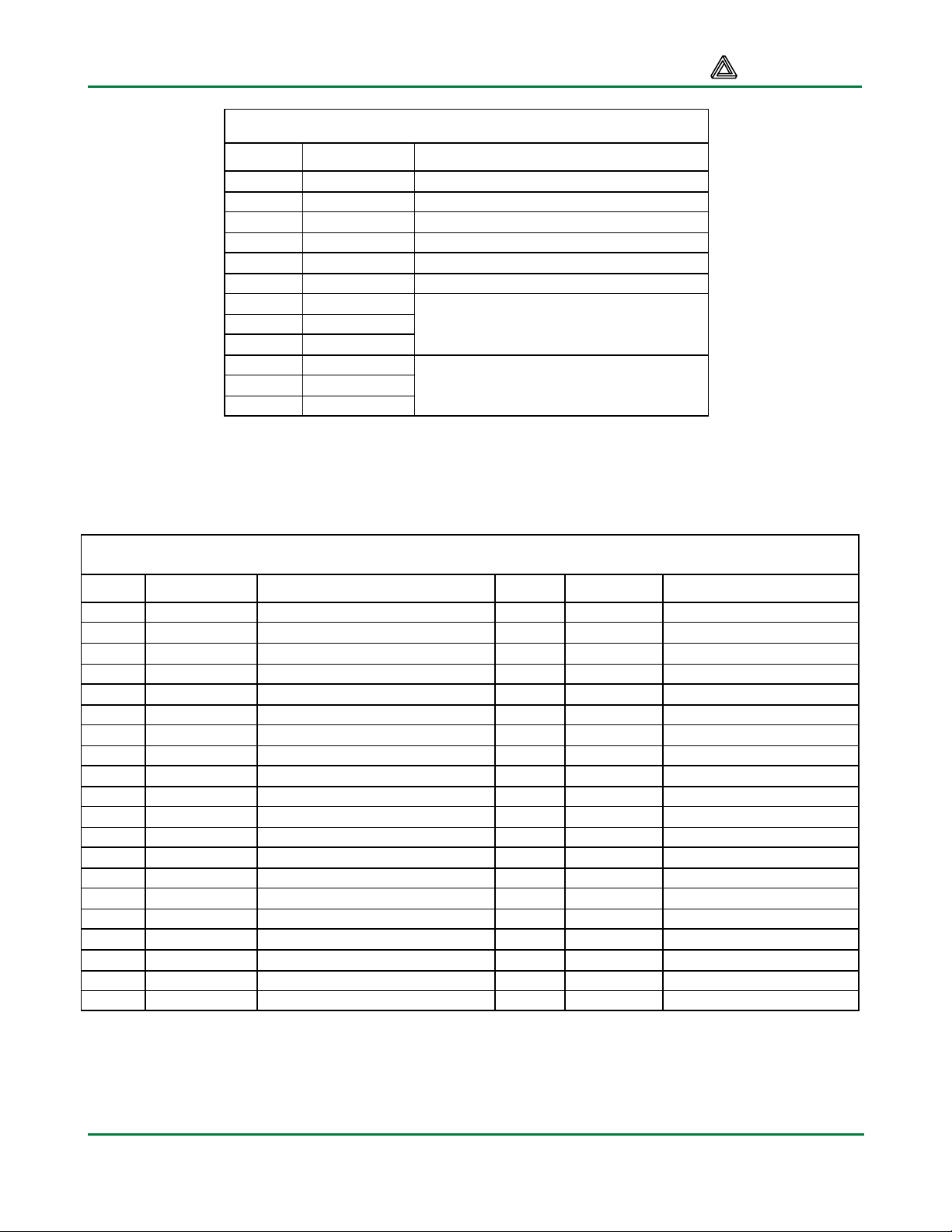
J2 connector pin definitions
J2 pin AIO signal Description
30 DACIN AD7303 data input
31 DACLK AD7303 clock input
29 SYNC AD7303 Sync signal
34 ADOUT AD7823 data output
33 CONVST AD7823 clock input
32 ADCLK AD7823 convert st art signal
38 DIN0
35 DIN1
36 DIN2
28 DOUT0
27 DOUT1
19 DOUT2
The breadboard connector signals are shown in the following table. The breadboard connector allows
various AIO1 signals to be connected to the breadboard using jumper wires. Signals from the BNC
connectors (J5 and J8), the RCA connectors (J6 and J9), and the audio connectors (J7 and J10) are
available, as well as signals from the op-amps and data converters.
Uncommitted digital inputs
Uncommitted digital outputs (use
caution – do not drive above 3.3V)
Breadboard Connector (J11) Signal Definitions
J11 pin
Signal Definition J11 pin Signal Definition
1 VCC33 Regulated voltage 21 OP2AO Op-amp 2A output
2 VU Unregulated voltage 22 OP2BO Op-amp 2B output
3 DI0 Uncommitted digital input 23 OP2BI+ Op-amp 2B input +
4 DO0 Uncommitted digital output 24 OP2BI- Op-amp 2B input 5 DI1 Uncommitted digital input 25 OP1BI+ Op-amp 1B input +
6 DO1 Uncommitted digital output 26 OP1BI- Op-amp 1B input 7 DI2 Uncommitted digital input 27 OP1BO Op-amp 1B output
8 DO2 Uncommitted digital output 28 OP1AO Op-amp 1A output
9 J8P BNC post connection 29 OP1AI+ Op-amp 1A input +
10 J8S BNC shield connection 30 OP1AI- Op-amp 1A input 11 J9P RCA center connection 31 GND System ground
12 J9S RCA shield connection 32 ADCREF ADC reference voltage
13 J10P Audio tip connection 33 ADCIN+ ADC input +
14 J10S Audio ring connections 34 ADCIN - ADC input 15 DACOUTA DAC channel A output 35 J7P Audio tip connection
16 DACOUTB DAC channel B output 36 J7S Audio ring connections
17 DACREF DAC reference voltage 37 J6P RCA center connection
18 GND System ground 38 J6S RCA shield connection
19 OP2AI+ Op-amp 2A input + 39 J5P BNC post connection
20 OP2AI- Op-amp 2A input - 40 J5S BNC shield connection
www.digilentinc.com Page 2
 Loading...