

Page 1

Xilinx University Program
Virtex-II Pro Development
System
Hardware Reference Manual
UG069 (v1.0) March 8, 2005
R
Page 2
R
"Xilinx" and the Xilinx logo shown above are registered trademarks of Xilinx, Inc. Any rights not expressly granted herein are reserved.
CoolRunner, RocketChips, Rocket IP, Spartan, StateBENCH, StateCAD, Virtex, XACT, XC2064, XC3090, XC4005, and XC5210 are
registered trademarks of Xilinx, Inc.
The shadow X shown above is a trademark of Xilinx, Inc.
ACE Controller, ACE Flash, A.K.A. Speed, Alliance Series, AllianceCORE, Bencher, ChipScope, Configurable Logic Cell, CORE Generator,
CoreLINX, Dual Block, EZTag, Fast CLK, Fast CONNECT, Fast FLASH, FastMap, Fast Zero Power, Foundation, Gigabit Speeds...and
Beyond!, HardWire, HDL Bencher, IRL, J Drive, JBits, LCA, LogiBLOX, Logic Cell, LogiCORE, LogicProfessor, MicroBlaze, MicroVia,
MultiLINX, NanoBlaze, PicoBlaze, PLUSASM, PowerGuide, PowerMaze, QPro, Real-PCI, RocketIO, SelectIO, SelectRAM, SelectRAM+,
Silicon Xpresso, Smartguide, Smart-IP, SmartSearch, SMARTswitch, System ACE, Testbench In A Minute, TrueMap, UIM, VectorMaze,
VersaBlock, VersaRing, Virtex-II Pro, Virtex-II EasyPath, Wave Table, WebFITTER, WebPACK, WebPOWERED, XABEL, XACTFloorplanner, XACT-Performance, XACTstep Advanced, XACTstep Foundry, XAM, XAPP, X-BLOX +, XC designated products, XChecker,
XDM, XEPLD, Xilinx Foundation Series, Xilinx XDTV, Xinfo, XSI, XtremeDSP and ZERO+ are trademarks of Xilinx, Inc.
The Programmable Logic Company is a service mark of Xilinx, Inc.
All other trademarks are the property of their respective owners.
Xilinx, Inc. does not assume any liability arising out of the application or use of any product described or shown herein; nor does it convey
any license under its patents, copyrights, or maskwork rights or any rights of others. Xilinx, Inc. reserves the right to make changes, at any
time, in order to improve reliability, function or design and to supply the best product possible. Xilinx, Inc. will not assume responsibility for
the use of any circuitry described herein other than circuitry entirely embodied in its products. Xilinx provides any design, code, or
information shown or described herein “as is.” By providing the design, code, or information as one possible implementation of a feature,
application, or standard, Xilinx makes no representation that such implementation is free from any claims of infringement. You are
responsible for obtaining any rights you may require for your implementation. Xilinx expressly disclaims any warranty whatsoever with
respect to the adequacy of any such implementation, including but not limited to any warranties or representations that the implementation
is free from claims of infringement, as well as any implied warranties of merchantability or fitness for a particular purpose. Xilinx, Inc. devices
and products are protected under U.S. Patents. Other U.S. and foreign patents pending. Xilinx, Inc. does not represent that devices shown
or products described herein are free from patent infringement or from any other third party right. Xilinx, Inc. assumes no obligation to
correct any errors contained herein or to advise any user of this text of any correction if such be made. Xilinx, Inc. will not assume any liability
for the accuracy or correctness of any engineering or software support or assistance provided to a user.
Xilinx products are not intended for use in life support appliances, devices, or systems. Use of a Xilinx product in such applications without
the written consent of the appropriate Xilinx officer is prohibited.
The contents of this manual are owned and copyrighted by Xilinx. Copyright 1994-2005 Xilinx, Inc. All Rights Reserved. Except as stated
herein, none of the material may be copied, reproduced, distributed, republished, downloaded, displayed, posted, or transmitted in any form
or by any means including, but not limited to, electronic, mechanical, photocopying, recording, or otherwise, without the prior written consent
of Xilinx. Any unauthorized use of any material contained in this manual may violate copyright laws, trademark laws, the laws of privacy and
publicity, and communications regulations and statutes.
XUP Virtex-II Pro Development System
UG069 (v1.0) March 8, 2005
The following table shows the revision history for this document.
Version Revision
03/08/05 1.0 Initial Xilinx release. (DRAFT)
XUP Virtex-II Pro Development System www.xilinx.com UG069 (v1.0) March 8, 2005
Page 3

Contents
Chapter 1: XUP Virtex-II Pro Development System
Features. . . . . . . . . . . . . . . . . . . . . . . . . . . . . . . . . . . . . . . . . . . . . . . . . . . . . . . . . . . . . . . . . . . . . 13
General Description. . . . . . . . . . . . . . . . . . . . . . . . . . . . . . . . . . . . . . . . . . . . . . . . . . . . . . . . . 14
Block Diagram . . . . . . . . . . . . . . . . . . . . . . . . . . . . . . . . . . . . . . . . . . . . . . . . . . . . . . . . . . . 14
Board Components . . . . . . . . . . . . . . . . . . . . . . . . . . . . . . . . . . . . . . . . . . . . . . . . . . . . . . . 14
Virtex-II Pro FPGA. . . . . . . . . . . . . . . . . . . . . . . . . . . . . . . . . . . . . . . . . . . . . . . . . . . . . . . . 15
Power Supplies and FPGA Configuration . . . . . . . . . . . . . . . . . . . . . . . . . . . . . . . . . . . . 16
Multi-Gigabit Transceivers . . . . . . . . . . . . . . . . . . . . . . . . . . . . . . . . . . . . . . . . . . . . . . . . . 17
System RAM . . . . . . . . . . . . . . . . . . . . . . . . . . . . . . . . . . . . . . . . . . . . . . . . . . . . . . . . . . . . . 17
System ACE Compact Flash Controller . . . . . . . . . . . . . . . . . . . . . . . . . . . . . . . . . . . . . . 17
Fast Ethernet Interface. . . . . . . . . . . . . . . . . . . . . . . . . . . . . . . . . . . . . . . . . . . . . . . . . . . . . 17
Serial Ports . . . . . . . . . . . . . . . . . . . . . . . . . . . . . . . . . . . . . . . . . . . . . . . . . . . . . . . . . . . . . . 17
User LEDs, Switches, and Push Buttons. . . . . . . . . . . . . . . . . . . . . . . . . . . . . . . . . . . . . . 18
Expansion Connectors . . . . . . . . . . . . . . . . . . . . . . . . . . . . . . . . . . . . . . . . . . . . . . . . . . . . . 18
XSGA Output . . . . . . . . . . . . . . . . . . . . . . . . . . . . . . . . . . . . . . . . . . . . . . . . . . . . . . . . . . . . 18
AC97 Audio CODEC . . . . . . . . . . . . . . . . . . . . . . . . . . . . . . . . . . . . . . . . . . . . . . . . . . . . . . 18
CPU Trace and Debug Port . . . . . . . . . . . . . . . . . . . . . . . . . . . . . . . . . . . . . . . . . . . . . . . . 18
USB 2 Programming Interface . . . . . . . . . . . . . . . . . . . . . . . . . . . . . . . . . . . . . . . . . . . . . . 18
Chapter 2: Using the System
Configuring the Power Supplies. . . . . . . . . . . . . . . . . . . . . . . . . . . . . . . . . . . . . . . . . . . . . 19
Configuring the FPGA . . . . . . . . . . . . . . . . . . . . . . . . . . . . . . . . . . . . . . . . . . . . . . . . . . . . . . 20
Clock Generation and Distribution . . . . . . . . . . . . . . . . . . . . . . . . . . . . . . . . . . . . . . . . . . 23
Using the DIMM Module DDR SDRAM . . . . . . . . . . . . . . . . . . . . . . . . . . . . . . . . . . . . 24
Using the XSGA Output. . . . . . . . . . . . . . . . . . . . . . . . . . . . . . . . . . . . . . . . . . . . . . . . . . . . . 34
Using the AC97 Audio CODEC and Power Amp . . . . . . . . . . . . . . . . . . . . . . . . . . . . . 39
Using the LEDs and Switches . . . . . . . . . . . . . . . . . . . . . . . . . . . . . . . . . . . . . . . . . . . . . . . 43
Using the Expansion Headers and Digilent Expansion Connectors . . . . . . . . . . . 44
Using the CPU Debug Port and CPU Reset. . . . . . . . . . . . . . . . . . . . . . . . . . . . . . . . . . . 58
Using the Serial Ports . . . . . . . . . . . . . . . . . . . . . . . . . . . . . . . . . . . . . . . . . . . . . . . . . . . . . . . 60
Using the Fast Ethernet Network Interface. . . . . . . . . . . . . . . . . . . . . . . . . . . . . . . . . . . 62
Using System ACE Controllers for Non-Volatile Storage. . . . . . . . . . . . . . . . . . . . . 65
Using the Multi-Gigabit Transceivers . . . . . . . . . . . . . . . . . . . . . . . . . . . . . . . . . . . . . . . 67
UG069 (v1.0) March 8, 2005 www.xilinx.com XUP Virtex-II Pro Development System
Page 4

Appendix A: Configuring the FPGA from the Embedded USB
Configuration Port
Appendix B: Programming the Platform FLASH PROM User Area
Appendix C: Restoring the Golden FPGA Configuration
Appendix D: Using the Golden FPGA Configuration for System Self-
Test
Hardware-Based Tests. . . . . . . . . . . . . . . . . . . . . . . . . . . . . . . . . . . . . . . . . . . . . . . . . . . . . . . 98
Power Supply and RESET Test . . . . . . . . . . . . . . . . . . . . . . . . . . . . . . . . . . . . . . . . . . . . . 98
Additional Hardware Required . . . . . . . . . . . . . . . . . . . . . . . . . . . . . . . . . . . . . . . . . . . 98
Test Procedure . . . . . . . . . . . . . . . . . . . . . . . . . . . . . . . . . . . . . . . . . . . . . . . . . . . . . . . . 98
Clock, Push Button, DIP Switch, LED, and Audio Amp Test . . . . . . . . . . . . . . . . . . . . 99
Additional Hardware Required . . . . . . . . . . . . . . . . . . . . . . . . . . . . . . . . . . . . . . . . . . . 99
Test Procedure . . . . . . . . . . . . . . . . . . . . . . . . . . . . . . . . . . . . . . . . . . . . . . . . . . . . . . . . 99
SVGA Gray Scale Test . . . . . . . . . . . . . . . . . . . . . . . . . . . . . . . . . . . . . . . . . . . . . . . . . . . . 100
Additional Hardware Required . . . . . . . . . . . . . . . . . . . . . . . . . . . . . . . . . . . . . . . . . . 100
Test Procedure . . . . . . . . . . . . . . . . . . . . . . . . . . . . . . . . . . . . . . . . . . . . . . . . . . . . . . . 100
SVGA Color Output Test . . . . . . . . . . . . . . . . . . . . . . . . . . . . . . . . . . . . . . . . . . . . . . . . . 100
Additional Hardware Required . . . . . . . . . . . . . . . . . . . . . . . . . . . . . . . . . . . . . . . . . . 100
Test Procedure . . . . . . . . . . . . . . . . . . . . . . . . . . . . . . . . . . . . . . . . . . . . . . . . . . . . . . . 100
Silicon Serial Number and PS/2 Serial Port Test . . . . . . . . . . . . . . . . . . . . . . . . . . . . . 101
Additional Hardware Required . . . . . . . . . . . . . . . . . . . . . . . . . . . . . . . . . . . . . . . . . . 101
Test Procedure . . . . . . . . . . . . . . . . . . . . . . . . . . . . . . . . . . . . . . . . . . . . . . . . . . . . . . . 101
Processor-Based Tests . . . . . . . . . . . . . . . . . . . . . . . . . . . . . . . . . . . . . . . . . . . . . . . . . . . . . . 101
Additional Hardware Required . . . . . . . . . . . . . . . . . . . . . . . . . . . . . . . . . . . . . . . . . . 102
MGT Serial ATA Test . . . . . . . . . . . . . . . . . . . . . . . . . . . . . . . . . . . . . . . . . . . . . . . . . . . . 102
Additional Hardware Required . . . . . . . . . . . . . . . . . . . . . . . . . . . . . . . . . . . . . . . . . . 102
EMAC Web Server Test. . . . . . . . . . . . . . . . . . . . . . . . . . . . . . . . . . . . . . . . . . . . . . . . . . . 106
Additional Hardware Required . . . . . . . . . . . . . . . . . . . . . . . . . . . . . . . . . . . . . . . . . . 106
EMAC Web Server Test Procedure . . . . . . . . . . . . . . . . . . . . . . . . . . . . . . . . . . . . . . . . 106
AC97 Audio Test . . . . . . . . . . . . . . . . . . . . . . . . . . . . . . . . . . . . . . . . . . . . . . . . . . . . . . . . 109
Additional Hardware Required . . . . . . . . . . . . . . . . . . . . . . . . . . . . . . . . . . . . . . . . . . 109
Digital Passthrough Test Procedure . . . . . . . . . . . . . . . . . . . . . . . . . . . . . . . . . . . . . . . 109
FIFO Loopback Test Procedure. . . . . . . . . . . . . . . . . . . . . . . . . . . . . . . . . . . . . . . . . . . 110
Game Sounds Test Procedure . . . . . . . . . . . . . . . . . . . . . . . . . . . . . . . . . . . . . . . . . . . . 110
System ACE Test . . . . . . . . . . . . . . . . . . . . . . . . . . . . . . . . . . . . . . . . . . . . . . . . . . . . . . . . 111
System ACE Test Procedure . . . . . . . . . . . . . . . . . . . . . . . . . . . . . . . . . . . . . . . . . . . . . 111
DDR SDRAM Test . . . . . . . . . . . . . . . . . . . . . . . . . . . . . . . . . . . . . . . . . . . . . . . . . . . . . . . 112
Additional Hardware Required . . . . . . . . . . . . . . . . . . . . . . . . . . . . . . . . . . . . . . . . . . 112
Test Procedure . . . . . . . . . . . . . . . . . . . . . . . . . . . . . . . . . . . . . . . . . . . . . . . . . . . . . . . 112
Expansion Port Test . . . . . . . . . . . . . . . . . . . . . . . . . . . . . . . . . . . . . . . . . . . . . . . . . . . . . . 113
Additional Hardware Required . . . . . . . . . . . . . . . . . . . . . . . . . . . . . . . . . . . . . . . . . . 113
Test Procedure . . . . . . . . . . . . . . . . . . . . . . . . . . . . . . . . . . . . . . . . . . . . . . . . . . . . . . . 113
XUP Virtex-II Pro Development System www.xilinx.com UG069 (v1.0) March 8, 2005
Page 5

Appendix E: User Constraint Files (UCF)
Appendix F: Links to the Component Data Sheets
FPGA Related Documentation. . . . . . . . . . . . . . . . . . . . . . . . . . . . . . . . . . . . . . . . . . . . . . 137
Configuration Sources . . . . . . . . . . . . . . . . . . . . . . . . . . . . . . . . . . . . . . . . . . . . . . . . . . . . . 137
DDR SDRAM Modules . . . . . . . . . . . . . . . . . . . . . . . . . . . . . . . . . . . . . . . . . . . . . . . . . . . . 137
Audio Processing . . . . . . . . . . . . . . . . . . . . . . . . . . . . . . . . . . . . . . . . . . . . . . . . . . . . . . . . . . 138
XSGA Video Output . . . . . . . . . . . . . . . . . . . . . . . . . . . . . . . . . . . . . . . . . . . . . . . . . . . . . . . 138
Ethernet Networking. . . . . . . . . . . . . . . . . . . . . . . . . . . . . . . . . . . . . . . . . . . . . . . . . . . . . . . 138
Power Supplies . . . . . . . . . . . . . . . . . . . . . . . . . . . . . . . . . . . . . . . . . . . . . . . . . . . . . . . . . . . . 138
UG069 (v1.0) March 8, 2005 www.xilinx.com XUP Virtex-II Pro Development System
Page 6

XUP Virtex-II Pro Development System www.xilinx.com UG069 (v1.0) March 8, 2005
Page 7

Figures
Chapter 1: XUP Virtex-II Pro Development System
Figure 1-1: XUP Virtex-II Pro Development System Block Diagram . . . . . . . . . . . . . . . . . 14
Figure 1-2: XUP Virtex-II Pro Development System Board Photo. . . . . . . . . . . . . . . . . . . . 15
Figure 1-3: I/O Bank Connections to Peripheral Devices . . . . . . . . . . . . . . . . . . . . . . . . . . . 16
Chapter 2: Using the System
Figure 2-1: Typical Switching Power Supply . . . . . . . . . . . . . . . . . . . . . . . . . . . . . . . . . . . . . 19
Figure 2-2: MGT Power . . . . . . . . . . . . . . . . . . . . . . . . . . . . . . . . . . . . . . . . . . . . . . . . . . . . . . . . 20
Figure 2-3: Configuration Data Path . . . . . . . . . . . . . . . . . . . . . . . . . . . . . . . . . . . . . . . . . . . . . 22
Figure 2-4: External Differential Clock Inputs . . . . . . . . . . . . . . . . . . . . . . . . . . . . . . . . . . . . 24
Figure 2-5: Alternate Clock Input Oscillator . . . . . . . . . . . . . . . . . . . . . . . . . . . . . . . . . . . . . . 24
Figure 2-6: Definition of Start and Stop Conditions . . . . . . . . . . . . . . . . . . . . . . . . . . . . . . . 25
Figure 2-7: Acknowledge Response from Receiver . . . . . . . . . . . . . . . . . . . . . . . . . . . . . . . . 26
Figure 2-8: EEPROM Sequential Read . . . . . . . . . . . . . . . . . . . . . . . . . . . . . . . . . . . . . . . . . . . 26
Figure 2-9: EEPROM Write . . . . . . . . . . . . . . . . . . . . . . . . . . . . . . . . . . . . . . . . . . . . . . . . . . . . . 26
Figure 2-10: Clock Generation for the DDR SDRAM . . . . . . . . . . . . . . . . . . . . . . . . . . . . . . 29
Figure 2-11: XSGA Output. . . . . . . . . . . . . . . . . . . . . . . . . . . . . . . . . . . . . . . . . . . . . . . . . . . . . . 36
Figure 2-12: AC97 Audio CODEC . . . . . . . . . . . . . . . . . . . . . . . . . . . . . . . . . . . . . . . . . . . . . . . 41
Figure 2-13: Audio Power Amplifier . . . . . . . . . . . . . . . . . . . . . . . . . . . . . . . . . . . . . . . . . . . . . 42
Figure 2-14: Expansion Headers . . . . . . . . . . . . . . . . . . . . . . . . . . . . . . . . . . . . . . . . . . . . . . . . . 44
Figure 2-15: CPU Debug Connector Pinouts . . . . . . . . . . . . . . . . . . . . . . . . . . . . . . . . . . . . . . 59
Figure 2-16: RELOAD and CPU RESET Circuit . . . . . . . . . . . . . . . . . . . . . . . . . . . . . . . . . . . 60
Figure 2-17: RS-232 Serial Port Implementation . . . . . . . . . . . . . . . . . . . . . . . . . . . . . . . . . . . 61
Figure 2-18: PS/2 Serial Port Implementation . . . . . . . . . . . . . . . . . . . . . . . . . . . . . . . . . . . . . 62
Figure 2-19: 10/100 Ethernet Interface Block Diagram . . . . . . . . . . . . . . . . . . . . . . . . . . . . . . 64
Figure 2-20: SMA-based MGT Connections . . . . . . . . . . . . . . . . . . . . . . . . . . . . . . . . . . . . . . 68
Figure 2-21: 1.5 Gb/s Serial Data Transmission over 0.5 meter of SATA Cable . . . . . . . . 70
Figure 2-22: 1.5 Gb/s Serial Data Transmission over 1.0 meter of SATA Cable . . . . . . . . 70
Appendix A: Configuring the FPGA from the Embedded USB
Configuration Port
Figure A-1: Device Manager Cable Entry . . . . . . . . . . . . . . . . . . . . . . . . . . . . . . . . . . . . . . . . . 72
Figure A-2: iMPACT Cable Selection Drop-Down Menu . . . . . . . . . . . . . . . . . . . . . . . . . . 72
Figure A-3: iMPACT Cable Communication Setup Dialog . . . . . . . . . . . . . . . . . . . . . . . . . 73
Figure A-4: Initializing the JTAG Chain. . . . . . . . . . . . . . . . . . . . . . . . . . . . . . . . . . . . . . . . . . 74
Figure A-5: Properly Identified JTAG Configuration Chain . . . . . . . . . . . . . . . . . . . . . . . . 75
Figure A-6: Assigning Configuration Files to Devices in the JTAG Chain . . . . . . . . . . . . 75
Figure A-7: Assigning a Configuration File to the FPGA . . . . . . . . . . . . . . . . . . . . . . . . . . . 76
UG069 (v1.0) March 8, 2005 www.xilinx.com XUP Virtex-II Pro Development System
Page 8

Figure A-8: Programming the FPGA . . . . . . . . . . . . . . . . . . . . . . . . . . . . . . . . . . . . . . . . . . . . . 76
Appendix B: Programming the Platform FLASH PROM User Area
Figure B-1: Operation Mode Selection: Prepare Configuration Files . . . . . . . . . . . . . . . . . 77
Figure B-2: Selecting PROM File . . . . . . . . . . . . . . . . . . . . . . . . . . . . . . . . . . . . . . . . . . . . . . . . 78
Figure B-3: Selecting a PROM with Design Revisioning Enabled . . . . . . . . . . . . . . . . . . . 79
Figure B-4: Selecting an XCF32P PROM with Two Revisions . . . . . . . . . . . . . . . . . . . . . . . 79
Figure B-5: Adding a Device File . . . . . . . . . . . . . . . . . . . . . . . . . . . . . . . . . . . . . . . . . . . . . . . . 80
Figure B-6: Adding the Design File to Revision 0. . . . . . . . . . . . . . . . . . . . . . . . . . . . . . . . . . 80
Figure B-7: iMPACT Startup Clock Warning. . . . . . . . . . . . . . . . . . . . . . . . . . . . . . . . . . . . . . 81
Figure B-8: Adding the Design File to Revision 1. . . . . . . . . . . . . . . . . . . . . . . . . . . . . . . . . . 81
Figure B-9: Generating the MCS File. . . . . . . . . . . . . . . . . . . . . . . . . . . . . . . . . . . . . . . . . . . . . 82
Figure B-10: Switching to Configuration Mode . . . . . . . . . . . . . . . . . . . . . . . . . . . . . . . . . . . 82
Figure B-11: Initializing the JTAG Chain . . . . . . . . . . . . . . . . . . . . . . . . . . . . . . . . . . . . . . . . . 83
Figure B-12: Assigning the MCS File to the PROM . . . . . . . . . . . . . . . . . . . . . . . . . . . . . . . . 83
Figure B-13: Programming the PROM. . . . . . . . . . . . . . . . . . . . . . . . . . . . . . . . . . . . . . . . . . . . 84
Figure B-14: PROM Programming Options . . . . . . . . . . . . . . . . . . . . . . . . . . . . . . . . . . . . . . . 85
Figure B-15: iMPACT PROM Programming Transcript Window . . . . . . . . . . . . . . . . . . . . 85
Appendix C: Restoring the Golden FPGA Configuration
Figure C-1: Operation Mode Selection: Configure Devices . . . . . . . . . . . . . . . . . . . . . . . . . 88
Figure C-2: Selecting Boundary Scan Mode. . . . . . . . . . . . . . . . . . . . . . . . . . . . . . . . . . . . . . . 89
Figure C-3: Boundary Scan Mode Selection: Automatically Connect to the Cable
and Identify the JTAG Chain . . . . . . . . . . . . . . . . . . . . . . . . . . . . . . . . . . . . . . . . . . . . . . . . 90
Figure C-4: Assigning New PROM Configuration File. . . . . . . . . . . . . . . . . . . . . . . . . . . . . 91
Figure C-5: Erasing the Existing PROM Contents . . . . . . . . . . . . . . . . . . . . . . . . . . . . . . . . . 92
Figure C-6: Transcript Window for the Erase Command . . . . . . . . . . . . . . . . . . . . . . . . . . . 92
Figure C-7: Selecting the Program Command . . . . . . . . . . . . . . . . . . . . . . . . . . . . . . . . . . . . . 93
Figure C-8: PROM Programming Options . . . . . . . . . . . . . . . . . . . . . . . . . . . . . . . . . . . . . . . . 94
Figure C-9: iMPACT PROM Programming Transcript Window. . . . . . . . . . . . . . . . . . . . . 95
Appendix D: Using the Golden FPGA Configuration for System Self-
Test
Figure D-1: XUP Virtex-II Pro Development System BIST Block Diagram . . . . . . . . . . . 97
Figure D-2: Built-In Self-Test Main Menu . . . . . . . . . . . . . . . . . . . . . . . . . . . . . . . . . . . . . . . 102
Figure D-3: Testing the SATA 0 HOST to SATA 1 TARGET Connection. . . . . . . . . . . . 103
Figure D-4: Testing the SATA 2 HOST to SATA 1 TARGET Connection. . . . . . . . . . . . 103
Figure D-5: Selecting the SATA Port Tests . . . . . . . . . . . . . . . . . . . . . . . . . . . . . . . . . . . . . . 104
Figure D-6: Selecting the Specific SATA Port to Test . . . . . . . . . . . . . . . . . . . . . . . . . . . . . 104
Figure D-7: Resetting the MGTs. . . . . . . . . . . . . . . . . . . . . . . . . . . . . . . . . . . . . . . . . . . . . . . . 104
Figure D-8: No Link Established Error Message. . . . . . . . . . . . . . . . . . . . . . . . . . . . . . . . . . 105
Figure D-9: SATA Test Running . . . . . . . . . . . . . . . . . . . . . . . . . . . . . . . . . . . . . . . . . . . . . . . 105
Figure D-10: SATA Loopback Test PASSED . . . . . . . . . . . . . . . . . . . . . . . . . . . . . . . . . . . . . 106
XUP Virtex-II Pro Development System www.xilinx.com UG069 (v1.0) March 8, 2005
Page 9

Figure D-11: Specifying IP Address for XUP Virtex-II Pro Development System. . . . . 107
Figure D-12: Web Server Running . . . . . . . . . . . . . . . . . . . . . . . . . . . . . . . . . . . . . . . . . . . . . . 107
Figure D-13: Web Server Display. . . . . . . . . . . . . . . . . . . . . . . . . . . . . . . . . . . . . . . . . . . . . . . 108
Figure D-14: Web Server Stopped . . . . . . . . . . . . . . . . . . . . . . . . . . . . . . . . . . . . . . . . . . . . . . 108
Figure D-15: Selecting the Specific AC97 Audio Test . . . . . . . . . . . . . . . . . . . . . . . . . . . . . 109
Figure D-16: Digital Passthrough Test Completion . . . . . . . . . . . . . . . . . . . . . . . . . . . . . . . 110
Figure D-17: FIFO Loopback Test Completion . . . . . . . . . . . . . . . . . . . . . . . . . . . . . . . . . . . 110
Figure D-18: Game Sounds Test Completion . . . . . . . . . . . . . . . . . . . . . . . . . . . . . . . . . . . . 111
Figure D-19: System ACE Test Completion . . . . . . . . . . . . . . . . . . . . . . . . . . . . . . . . . . . . . . 111
Figure D-20: DDR SDRAM Test Completion . . . . . . . . . . . . . . . . . . . . . . . . . . . . . . . . . . . . 113
Figure D-21: Confirming Start of the Expansion Port Walking Ones Test . . . . . . . . . . . 114
Appendix E: User Constraint Files (UCF)
Appendix F: Links to the Component Data Sheets
UG069 (v1.0) March 8, 2005 www.xilinx.com XUP Virtex-II Pro Development System
Page 10

XUP Virtex-II Pro Development System www.xilinx.com UG069 (v1.0) March 8, 2005
Page 11

Tables
Chapter 1: XUP Virtex-II Pro Development System
Chapter 2: Using the System
Table 1-1: XC2VP20 and XC2VP30 Device Features . . . . . . . . . . . . . . . . . . . . . . . . . . . . . . . 15
Table 2-1: System Configuration Status LEDs. . . . . . . . . . . . . . . . . . . . . . . . . . . . . . . . . . . . . 22
Table 2-2: Clock Connections . . . . . . . . . . . . . . . . . . . . . . . . . . . . . . . . . . . . . . . . . . . . . . . . . . . 23
Table 2-3: SPD EEPROM Contents . . . . . . . . . . . . . . . . . . . . . . . . . . . . . . . . . . . . . . . . . . . . . . 27
Table 2-4: Qualified SDRAM Memory Modules . . . . . . . . . . . . . . . . . . . . . . . . . . . . . . . . . . 30
Table 2-5: DDR SDRAM Connections . . . . . . . . . . . . . . . . . . . . . . . . . . . . . . . . . . . . . . . . . . . 30
Table 2-6: DCM and XSGA Controller Settings for Various XSGA Formats . . . . . . . . . . 37
Table 2-7: XSGA Output Connections. . . . . . . . . . . . . . . . . . . . . . . . . . . . . . . . . . . . . . . . . . . . 38
Table 2-8: AC97 Audio CODEC Connections . . . . . . . . . . . . . . . . . . . . . . . . . . . . . . . . . . . . . 43
Table 2-9: User LED and Switch Connections . . . . . . . . . . . . . . . . . . . . . . . . . . . . . . . . . . . . . 43
Table 2-10: Top Expansion Header Pinout . . . . . . . . . . . . . . . . . . . . . . . . . . . . . . . . . . . . . . . . 45
Table 2-11: Upper Middle Expansion Header Pinout. . . . . . . . . . . . . . . . . . . . . . . . . . . . . . . 47
Table 2-12: Lower Middle Expansion Header Pinout. . . . . . . . . . . . . . . . . . . . . . . . . . . . . . . 49
Table 2-13: Bottom Expansion Header Pinout . . . . . . . . . . . . . . . . . . . . . . . . . . . . . . . . . . . . . 51
Table 2-14: Left Digilent Expansion Connector Pinout . . . . . . . . . . . . . . . . . . . . . . . . . . . . . 53
Table 2-15: Right Digilent Expansion Connector Pinout. . . . . . . . . . . . . . . . . . . . . . . . . . . . 54
Table 2-16: High-Speed Digilent Expansion Connector Pinout. . . . . . . . . . . . . . . . . . . . . . 56
Table 2-17: CPU Debug Port Connections and CPU Reset . . . . . . . . . . . . . . . . . . . . . . . . . . 59
Table 2-18: Keyboard, Mouse, and RS-232 Connections . . . . . . . . . . . . . . . . . . . . . . . . . . . . 62
Table 2-19: 10/100 ETHERNET Connections . . . . . . . . . . . . . . . . . . . . . . . . . . . . . . . . . . . . . . 64
Table 2-20: System ACE Connections . . . . . . . . . . . . . . . . . . . . . . . . . . . . . . . . . . . . . . . . . . . . 66
Table 2-21: SATA and MGT Signals . . . . . . . . . . . . . . . . . . . . . . . . . . . . . . . . . . . . . . . . . . . . . 68
UG069 (v1.0) March 8, 2005 www.xilinx.com XUP Virtex-II Pro Development System
Page 12

Appendix A: Configuring the FPGA from the Embedded USB
Configuration Port
Appendix B: Programming the Platform FLASH PROM User Area
Appendix C: Restoring the Golden FPGA Configuration
Appendix D: Using the Golden FPGA Configuration for System Self-
Test
Appendix E: User Constraint Files (UCF)
Appendix F: Links to the Component Data Sheets
XUP Virtex-II Pro Development System www.xilinx.com UG069 (v1.0) March 8, 2005
Page 13

R
Chapter 1
XUP Virtex-II Pro Development System
Features
• Virtex™-II Pro FPGA with PowerPC™ 405 cores
• Up to 2 GB of Double Data Rate (DDR) SDRAM
• System ACE™ controller and Type II CompactFlash™ connector for FPGA
configuration and data storage
• Embedded Platform Cable USB configuration port
• High-speed SelectMAP FPGA configuration from Platform Flash In-System
Programmable Configuration PROM
• Support for “Golden” and “User” FPGA configuration bitstreams
• On-board 10/100 Ethernet PHY device
• Silicon Serial Number for unique board identification
• RS-232 DB9 serial port
• Two PS-2 serial ports
• Four LEDs connected to Virtex-II Pro I/O pins
• Four switches connected to Virtex-II Pro I/O pins
• Five push buttons connected to Virtex-II Pro I/O pins
• Six expansion connectors joined to 80 Virtex-II Pro I/O pins with over-voltage
protection
• High-speed expansion connector joined to 40 Virtex-II Pro I/O pins that can be used
differentially or single ended
• AC-97 audio CODEC with audio amplifier and speaker/headphone output and line
level output
• Microphone and line level audio input
• On-board XSGA output, up to 1200 x 1600 at 70 Hz refresh
• Three Serial ATA ports, two Host ports and one Target port
• Off-board expansion MGT link, with user-supplied clock
• 100 MHz system clock, 75 MHz SATA clock
• Provision for user-supplied clock
• On-board power supplies
• Power-on reset circuitry
• PowerPC 405 reset circuitry
XUP Virtex-II Pro Development System www.xilinx.com 13
UG069 (v1.0) March 8, 2005
Page 14
R
General Description
The XUP Virtex-II Pro Development System provides an advanced hardware platform that
consists of a high performance Virtex-II Pro Platform FPGA surrounded by a
comprehensive collection of peripheral components that can be used to create a complex
system and to demonstrate the capability of the Virtex-II Pro Platform FPGA.
Block Diagram
Figure 1-1 shows a block diagram of the XUP Virtex-II Pro Development System.
Chapter 1: XUP Virtex-II Pro Development System
External Power
Internal Power Supplies
4.5-5.5V
CPU Debug Port
100 MHz System Clock
75 MHz SATA Clock
User Clocks (2)
Platform Flash Configurations (2)
Compact Flash Configurations (8)
USB2 High Speed Configuration
3.3V
2.5V
1.5V
Figure 1-1: XUP Virtex-II Pro Development System Block Diagram
Board Components
Virtex-II Pro
FPGA
AC97 Audio CODEC & Stereo Amp
XSGA Video Output
User LEDs (4)
User Switches (4)
User Push-button Switches (5)
10/100 Ethernet PHY
RS-232 & PS/2 Ports (2)
Serial ATA Por ts (3)
Multi-Gigabit Transceiver Port
2 GB DDR SDRAM DIMM Module
5V Tolerant Expansion Headers
High Speed Expansion Port
UG069_01_012105
This section contains a concise overview of several important components on the XUP
Virtex-II Pro Development System (see Figure 1-2). The most recent documentation for the
system can be obtained from the XUP Virtex-II Pro Development System support website
at: http://www.xilinx.com/univ/xup2vp.html
14 www.xilinx.com XUP Virtex-II Pro Development System
UG069 (v1.0) March 8, 2005
Page 15
General Description
R
Figure 1-2: XUP Virtex-II Pro Development System Board Photo
Virtex-II Pro FPGA
U1 is a Virtex-II Pro FPGA device packaged in a flip-chip-fine-pitch FF896 BGA package.
Two different capacity FPGAs can be used on the XUP Virtex-II Pro Development System
with no change in functionality. Ta bl e 1-1 lists the Virtex-II Pro device features.
Table 1-1: XC2VP20 and XC2VP30 Device Features
Features XC2VP20 XC2VP30
Slices 9280 13969
Array Size 56 x 46 80 x 46
Distributed RAM 290 Kb 428 Kb
Multiplier Blocks 88 136
XUP Virtex-II Pro Development System www.xilinx.com 15
UG069 (v1.0) March 8, 2005
Page 16
R
Chapter 1: XUP Virtex-II Pro Development System
Table 1-1: XC2VP20 and XC2VP30 Device Features (Continued)
Features XC2VP20 XC2VP30
Block RAMs 1584 Kb 2448 Kb
DCMs 8 8
PowerPC RISC Cores 2 2
Multi-Gigabit Transceivers 8 8
Figure 1-3 identifies the I/O banks that are used to connect the various peripheral devices
to the FPGA.
AC97 Audio SXGA port
10/100 Ethernet
1
0
2
7
OVER VOLTAGE CLAMPS
EXPANSION CONNECTORS
LEDs & SWITCHES
PS/2 KBD & MOUSE
PUSH BUTTONS
RS-232
System ACE port
Figure 1-3: I/O Bank Connections to Peripheral Devices
Power Supplies and FPGA Configuration
The XUP Virtex-II Pro Development System is powered from a 5V regulated power supply.
On-board switching power supplies generate 3.3V, 2.5V, and 1.5V for the FPGA, and
peripheral components and linear regulators power the MGTs.
The board has provisioning for current measurement for all of the FPGA digital power
supplies, as well as application of external power if the capacity of the on-board switching
power supplies is exceeded.
3
6
45
256M x 64/72 DDR SDRAM DIMM MODULE
3.3V IO
2.5V IO
UG069_03_012105
The XUP Virtex-II Pro Development System provides several methods for the
configuration of the Virtex-II Pro FPGA. The configuration data can originate from the
internal Platform Flash PROM (two potential configurations), the internal CompactFlash
storage media (eight potential configurations), and external configurations delivered from
the embedded Platform Cable USB or parallel port interface.
16 www.xilinx.com XUP Virtex-II Pro Development System
UG069 (v1.0) March 8, 2005
Page 17

General Description
Multi-Gigabit Transceivers
System RAM
R
Four of the eight Multi-Gigabit Transceivers (MGTs) that are present in the Virtex-II Pro
FPGA are brought out to connectors and can be utilized by the user. Three of the
bidirectional MGT channels are terminated at Serial Advanced Technology Attachment
(SATA) connectors and the fourth channel terminates at user-supplied Sub-Miniature A
(SMA) connectors. The MGT transceivers are equipped with a 75 MHz clock source that is
independent for the system clock to support standard SATA communication. An
additional MGT clock source is available through a differential user-supplied (SMA)
connector pair. Two of the ports with SATA connectors are configured as Host ports and
the third SATA port is configured as a Target port to allow for simple board-to-board
networking.
The XUP Virtex-II Pro Development System has provision for the installation of usersupplied JEDEC-standard 184-pin dual in-line Double Data Rate Synchronous Dynamic
RAM memory module. The board supports buffered and unbuffered memory modules
with a capacity of 2 GB or less in either 64-bit or 72-bit organizations. The 72-bit
organization should be used if ECC error detection and correction is required.
System ACE Compact Flash Controller
The System Advanced Configuration Environment (System ACE™) Controller manages
FPGA configuration data. The controller provides an intelligent interface between an
FPGA target chain and various supported configuration sources. The controller has several
ports: the Compact Flash port, the Configuration JTAG port, the Microprocessor (MPU)
port and the Test JTAG port. The XUP Virtex-II Pro Development System supports a single
System ACE Controller. The Configuration JTAG ports connect to the FPGA and front
expansion connectors. The Test JTAG port connects to the JTAG port header and USB2
interface CPLD, and the MPU ports connect directly to the FPGA.
Fast Ethernet Interface
The XUP Virtex-II Pro Development System provides an IEEE-compliant Fast Ethernet
transceiver that supports both 100BASE-TX and 10BASE-T applications. It supports full
duplex operation at 10 Mb/s and 100 Mb/s, with auto-negotiation and parallel detection.
The PHY provides a Media Independent Interface (MII) for attachment to the 10/100
Media Access Controller (MAC) implemented in the FPGA. Each board is equipped with a
Silicon Serial Number that uniquely identifies each board with a 48-bit serial number. This
serial number is retrieved using “1-Wire” protocol. This serial number can be used as the
system MAC address.
Serial Ports
The XUP Virtex-II Pro Development System provides three serial ports: a single RS-232
port and two PS/2 ports. The RS-232 port is configured as a DCE with hardware
handshake using a standard DB-9 serial connector. This connector is typically used for
communications with a host computer using a standard 9-pin serial cable connected to a
COM port. The two PS/2 ports could be used to attach a keyboard and mouse to the XUP
Virtex-II Pro Development System. All of the serial ports are equipped with level-shifting
circuits, because the Virtex-II Pro FPGAs cannot interface directly to the voltage levels
required by RS-232 or PS/2.
XUP Virtex-II Pro Development System www.xilinx.com 17
UG069 (v1.0) March 8, 2005
Page 18

R
Chapter 1: XUP Virtex-II Pro Development System
User LEDs, Switches, and Push Buttons
A total of four LEDs are provided for user-defined purposes. When the FPGA drives a
logic 0, the corresponding LED turns on. A single four-position DIP switch and five push
buttons are provided for user input. If the DIP switch is up, closed, or on, or the push button
is pressed, a logic 0 is seen by the FPGA, otherwise a logic 1 is indicated.
Expansion Connectors
A total of 80 Virtex-II Pro I/O pins are brought out to four user-supplied 60-pin headers
and two 40-pin right angle connectors for user-defined use. The 60-pin headers are
designed to accept ribbon-cable connectors, with every second signal a ground for signal
integrity. Some of these signals are shared with the front-mounted right-angle connectors.
The front-mounted connectors support Digilent expansion modules. In addition, a highspeed connector is provided to support Digilent high-speed expansion modules. This
connector provides 40 single-ended or differential I/O signals in addition to three clocks.
Consult the Digilent website at www.diglentinc.com
compatible with the XUP Virtex-II Pro Development System.
XSGA Output
The XUP Virtex-II Pro Development System includes a video DAC and 15-pin highdensity D-sub connector to support XSGA output. The video DAC can operate with a pixel
clock of up to 180 MHz. This allows for a VESA-compatible output of 1280 x 1024 at 75 Hz
refresh and a maximum resolution of 1600 x 1200 at 70 Hz refresh.
for a list of expansion boards that are
AC97 Audio CODEC
An audio CODEC and stereo power amplifier are included on the XUP Virtex-II Pro
Development System to provide a high-quality audio path and provide all of the analog
functionality in a PC audio system. It features a full-duplex stereo ADC and DAC, with an
analog mixer, combining the line-level inputs, microphone input, and PCM data.
CPU Trace and Debug Port
The FPGA is equipped with a CPU debugging interface and a 16-pin header. This
connector can be used in conjunction with third party tools, the Xilinx Parallel Cable IV, or
the Xilinx Platform Cable USB to debug software as it runs on either PowerPC 405
processor core.
ChipScope Pro™ can also be used to perform real-time debug and verification of the FPGA
design. ChipScope Pro inserts logic analyzer, bus analyzer, and Virtual I/O low-profile
software cores into the FPGA design. These cores allow the designer to view all the internal
signals and nodes within the FPGA including the Processor Local Bus (PLB) or On-Chip
Peripheral Bus (OPB) supporting the PowerPC 405 cores. Signals are captured and brought
out through the embedded Platform Cable USB programming interface for analysis using
the ChipScope Pro Logic Analyzer tool.
USB 2 Programming Interface
The XUP Virtex-II Pro Development System includes an embedded USB 2.0
microcontroller capable of communications with either high-speed (480 Mb/s) or fullspeed (12 Mb/s) USB hosts. This interface is used for programming or configuring the
Virtex-II Pro FPGA in Boundary-Scan (IEEE 1149.1/IEEE 1532) mode. Target clock speeds
are selectable from 750 kHz to 24 MHz. The USB 2.0 microcontroller attaches to a desktop
or laptop PC with an off-the-shelf high-speed A-B USB cable.
18 www.xilinx.com XUP Virtex-II Pro Development System
UG069 (v1.0) March 8, 2005
Page 19
R
Using the System
Configuring the Power Supplies
The XUP Virtex-II Pro Development System supports the independent creation of the
power supplies for the core voltage of 1.5V (FPGA_VINT), 2.5V general-purpose power,
I/O and/or VCCAUX supplies (VCC2V5), and 3.3V I/O and general-purpose power
(VCC3V3). These voltages are created by synchronous buck-switching regulators derived
from the 4.5V-5.5V power input provided at the center-positive barrel-jack power input
(J26) or the terminal block pair (J34-J35). Each of these supplies can be disabled through the
insertion of jumpers (JP2, JP4, and JP6), and the external application of power from the
terminal blocks (J28-J33). If external power is supplied, the associated internal power
supply must be disabled (through the insertion of JP6, JP2, or JP4) and the associated onboard power delivery jumpers (JP5, JP1, or JP3) must be removed. The power consumption
from each of the on-board power supplies can be monitored through the removal of JP5,
JP1, or JP3 and the insertion of a current monitor. If any of the power supplies are outside
the recommended tolerance, internally or externally provided, the system enters a RESET
state indicated by the illumination of the RESET_PS_ERROR LED (D6) and the assertion of
the RESET_Z signal. A typical switching power supply is shown in Figure 2-1.
Chapter 2
ug069_04_021505
Figure 2-1: Typical Switching Power Supply
XUP Virtex-II Pro Development System www.xilinx.com 19
UG069 (v1.0) March 8, 2005
Page 20
VCC3V3
R
Chapter 2: Using the System
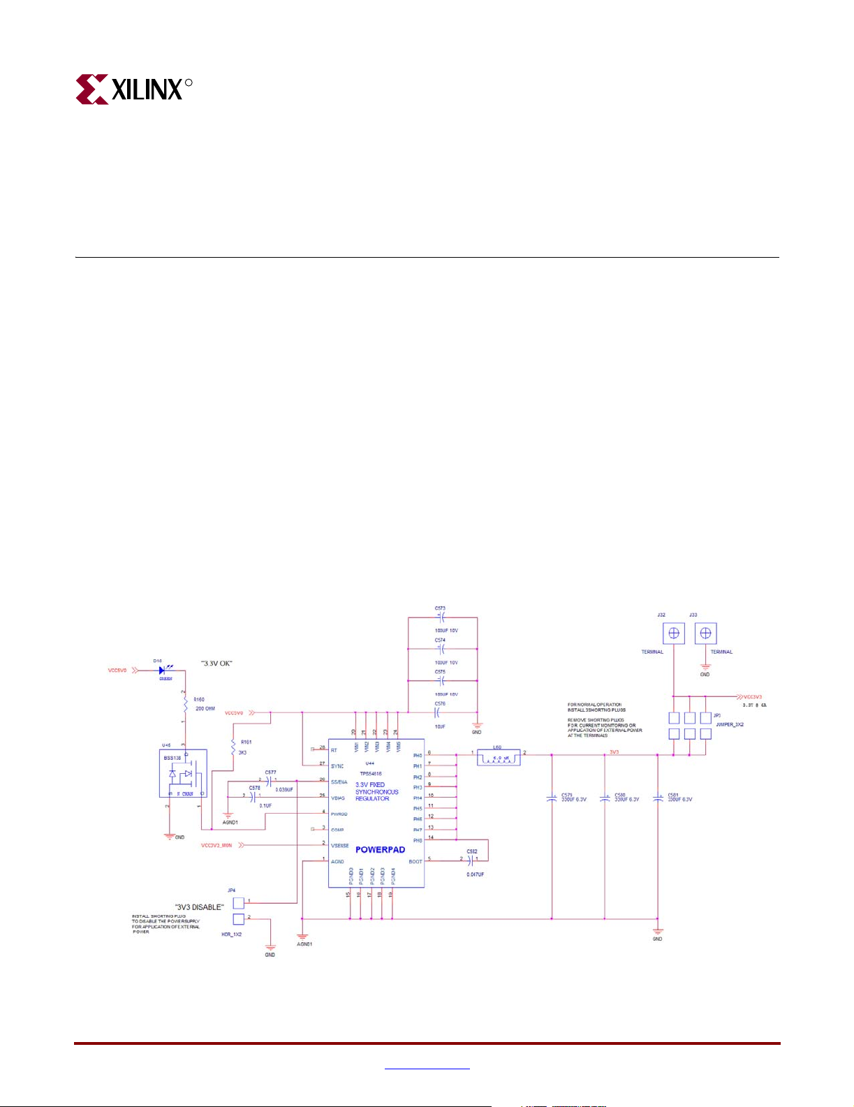
Because of the analog nature of the MGTs, the power for those elements are created by low
noise, low dropout linear regulators. Figure 2-2 shows the power supply for the MGTs.
U20
FIXED 2.5V LDO
TA B
TA B
4
3
+
6
4
3
6
C428
330UF 6.3V
C433
+
330UF 6.3V
C430
0.1UF
C434
0.1UF
VCC_MGT
C427
1000PF
VTT_MGT
C432
1000PF
UG069_05_010605
C431
+
33OUF 6.3V
C429
+
33OUF 6.3V
FERRITE BEAD
2961666671
L32
2
IN OUT
1
SHDN GND
5
SENSE
LT1963AEQ-25
U21
FIXED 2.5V LDO
2
IN OUT
1
SHDN GND
5
SENSE
LT1963AEQ-25
GND_MGT
Configuring the FPGA
At power up, or when the RESET_RELOAD push button (SW1) is pressed for longer than
2 seconds, the FPGA begins to configure. The two configuration methods supported, JTAG
and master SelectMAP, are determined by the CONFIG SOURCE switch, the most
significant switch (left side) of SW9.
If the CONFIG SOURCE switch is closed, on, or up, a high-speed SelectMap byte-wide
configuration from the on-board Platform Flash configuration PROM (U3) is selected as
the configuration source. This is identified to the user through the illumination of the
PROM CONFIG LED (D19).
The Platform Flash configuration PROM supports two different FPGA configurations
(versions) selected by the position of the PROM VERSION switch, the least significant
switch (right side) of SW9.
If the PROM VERSION switch is closed, on, or up, the GOLDEN configuration from the onboard Platform Flash configuration PROM is selected as the configuration data. This is
identified to the user through the illumination of the GOLDEN CONFIG LED (D14). This
configuration can be a board test utility provided by Xilinx, or another safe default
configuration. It is important to note that the PROM VERSION switch is only sampled on
board powerup and after a complete system reset. This means that if this switch is changed
after board powerup, the RESET_RELOAD pushbutton (SW1) must be pressed for more
than 2 seconds for the new state of the switch to be recognized.
Figure 2-2: MGT Power
If the PROM VERSION switch is open, off, or down, a User configuration from the on-board
Platform Flash configuration PROM is selected as the configuration data. This
configuration must be programmed into the Platform Flash PROM from the JTAG
Platform Cable USB interface or the USB interface following the instructions in Appendix
B, “Programming the Platform FLASH PROM User Area.”
20 www.xilinx.com XUP Virtex-II Pro Development System
UG069 (v1.0) March 8, 2005
Page 21

Configuring the FPGA
The Platform Flash is normally disabled after the FPGA is finished configuring and has
asserted the DONE signal. If additional data is made available to the FPGA after the
completion of configuration, jumper JP9 must be moved from the NORMAL to the
EXTENDED position to permanently enable the PROM and allow the FPGA to clock out
the additional data using the FPGA_PROM_CLOCK signal. The process of loading
additional non-configuration data into the FPGA is outlined in application note:
XAPP694:
Reading User Data from Configuration PROMs.
If the CONFIG SOURCE switch is open, off, or down, a lower speed JTAG-based
configuration from Compact Flash or external JTAG source is selected as the configuration
source. This is identified to the user through the illumination of the JTAG CONFIG LED
(D20).
The JTAG-based configuration can originate from several sources: the Compact Flash card,
a PC4 cable connection through J27, and a USB to PC connection through J8 the embedded
Platform Cable USB interface.
If a JTAG-based configuration is selected, the default source is from the Compact Flash
port (J7). The System ACE controller checks the associated Compact Flash socket and
storage device for the existence of configuration data. If configuration data exists on the
storage device, the storage device becomes the source for the configuration data. The file
structure on the Compact Flash storage device supports up to eight different configuration
data files, selected by the triple CF CONFIG SELECT DIP switch (SW8). During JTAG
configuration, the SYSTEMACE STATUS LED (D12) flashes until the configuration process
is completed, and the FPGA asserts the FPGA_DONE signal and illuminates the DONE
LED (D4). At any time, the RESET_RELOAD pushbutton (SW1) can be used to load any of
the eight different configuration data files by pressing the switch for more than 2 seconds.
R
If a JTAG-based configuration is selected and a valid configuration file is not found on the
Compact Flash card by the System ACE controller (U2), the SYSTEMACE ERROR LED
(D11) flashes, and the System ACE controller connects to an external JTAG port for FPGA
configuration.
The default external source for FPGA configuration is the high-speed embedded Platform
Cable USB configuration port (J8) and is enabled when the System ACE controller does not
find configuration data on the storage device. Detailed instructions on using the highspeed Platform Cable USB interface can be found in Appendix A, “Configuring the FPGA
from the Embedded USB Configuration Port.”
If a USB-equipped host PC is not available as a configuration source, then a Parallel Cable
4 (PC4) interface can be used instead by connecting a PC4 cable to J27.
It should be noted that if SelectMap byte-wide configuration from the on-board Platform
Flash configuration PROM is enabled, the FPGA Start-Up Clock should be set to CCLK in
the Startup Options section of the Process Options for the generation of the programming
file, otherwise JTAG Clock should be selected.
XUP Virtex-II Pro Development System www.xilinx.com 21
UG069 (v1.0) March 8, 2005
Page 22

R
Chapter 2: Using the System
Figure 2-3 illustrates the configuration data path.
USB2
Microcontroller
& CPLD
GOLDEN
VERSION SELECT
USER
JTAG Port
JTAG Port
PLATFORM
FLASH
SMAP Port
Test JTAG Port Config JTAG Port
SystemACE
Controller
PROM
CONFIG SOURCE
JTAG
CF Card/
MicroDrive
SMAP Port
Micro Port
CF CONFIG SELECT
FPGA
Micro PortJTAG Port
UG069_06_122704
Figure 2-3: Configuration Data Path
Four status LEDs show the configuration state of the XUP Virtex-II Pro Development
System at all times. The user can see the configuration source, configuration version, and
tell when the configuration has completed from the status LEDs shown in Tab le 2- 1.
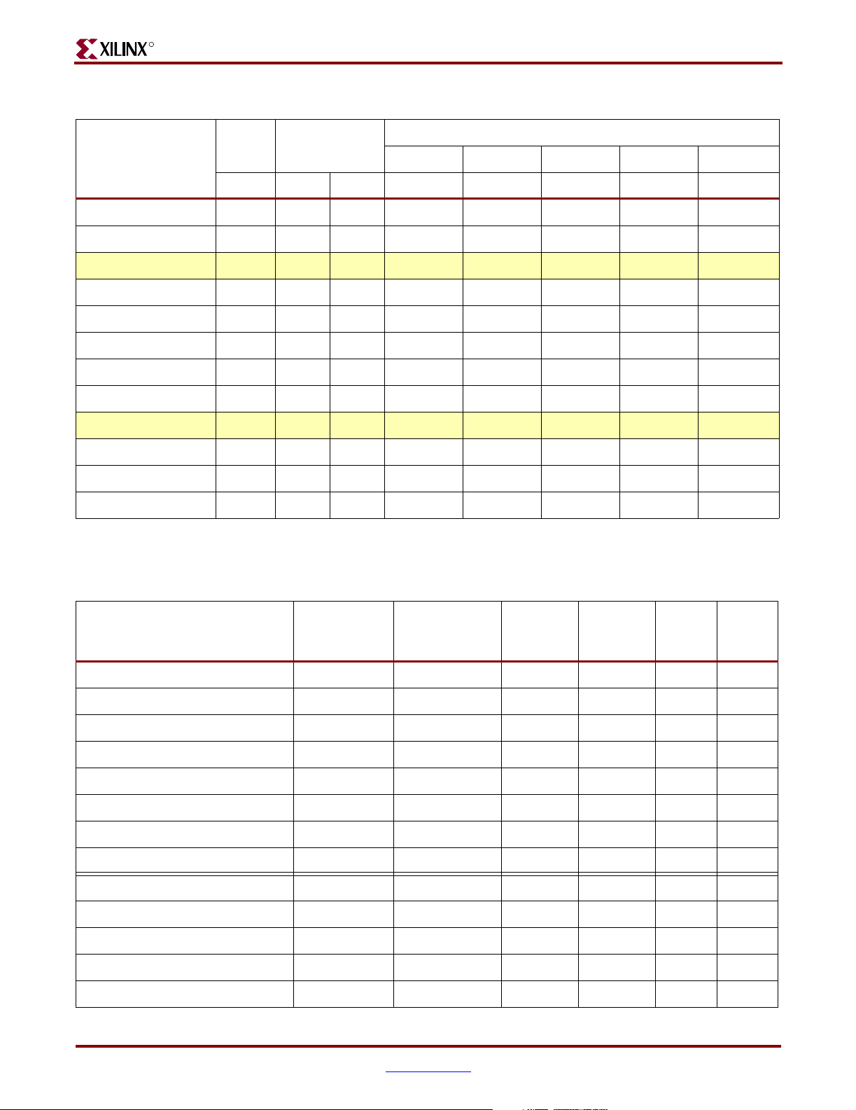
Table 2-1: System Configuration Status LEDs
LED Status
System Status
D19 (Green)
PROM Config
D20 (Green)
CF Config
D14 (Amber)
GOLDEN Config
D4 (Red)
Done
SelectMAP USER LOADING ON OFF OFF OFF
SelectMAP USER COMPLETED ON OFF OFF ON
SelectMAP GOLDEN LOADING ON OFF ON OFF
SelectMAP GOLDEN
ON OFF ON ON
COMPLETED
JTAG COMPACT FLASH
OFF ON OFF OFF
LOADING
JTAG COMPACT FLASH
OFF ON OFF ON
COMPLETED
22 www.xilinx.com XUP Virtex-II Pro Development System
UG069 (v1.0) March 8, 2005
Page 23
Clock Generation and Distribution
Table 2-1: System Configuration Status LEDs (Continued)
LED Status
System Status
D19 (Green)
PROM Config
D20 (Green)
CF Config
D14 (Amber)
GOLDEN Config
D4 (Red)
Done
JTAG USB or PC4 LOADING OFF ON OFF OFF
JTAG USB or PC4 COMPLETED OFF ON OFF ON
Clock Generation and Distribution
The XUP Virtex-II Pro Development System supports six clock sources:
• A 100 MHz system clock (Y2),
• A 75 MHz clock (U10) for the MGTs operating the Serial Advanced Technology
Attachment (SATA) ports,
• A dual footprint through-hole user-supplied alternate clock (Y3),
• An external clock for the MGTs (J23-J24),
• A 32 MHz clock (Y4) for the System ACE interfaces, and
• A clock from the Digilent high-speed expansion module.
R
The 75 MHz SATA clock is obtained from a high stability (20 ppm) 3.3V LVDSL differential
output oscillator, and the external MGT clock is obtained from two user-supplied SMA
connectors. The remaining three oscillators are all 3.3V single-ended LVTTL sources. Each
of the oscillators is equipped with a power supply filter to reduce the noise on the clock
outputs.
Tab le 2 -2 identifies the various clock connections for the FPGA.
Table 2-2: Clock Connections
Signal FPGA Pin I/O Type
SYSTEM_CLOCK AJ15 LVCMOS25
ALTERNATE_CLOCK AH16 LVCMOS25
HS_CLKIN (from high speed
B16 LVCMOS25
expansion port)
MGT_CLK_P F16 LVDS_25
MGT_CLK_N G16 LVDS_25
EXTERNAL_CLOCK_P G15 LVDS_25
EXTERNAL_CLOCK_N F15 LVDS_25
FPGA_SYSTEMACE_CLOCK AH15 LVCMOS25
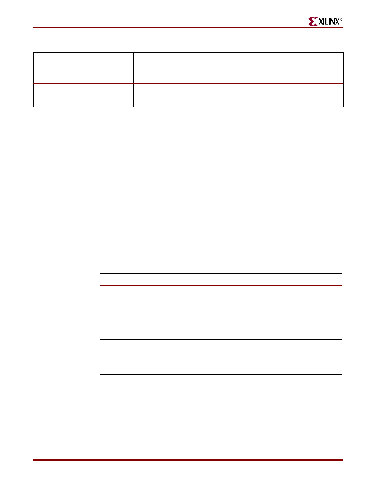
For the user to take advantage of the external differential clock inputs, two SMA
connectors must be installed at J23 and J24. These SMA connectors can be purchased from
Digi-Key® under the part number A24691-ND. Figure 2-4 identifies the location of the
external differential clock inputs.
XUP Virtex-II Pro Development System www.xilinx.com 23
UG069 (v1.0) March 8, 2005
Page 24
R
Chapter 2: Using the System
Figure 2-4: External Differential Clock Inputs
The alternate clock input is obtained from a user-supplied 3.3V oscillator. The footprint on
the printed circuit board supports either a full size (21mm x 13mm) or half size (13mm x
13mm) through-hole oscillator. Figure 2-5 identifies the location of the alternate clock
input oscillator.
Figure 2-5: Alternate Clock Input Oscillator
Using the DIMM Module DDR SDRAM
The XUP Virtex-II Pro Development System is equipped with a 184-pin Dual In-line
Memory Module (DIMM) socket that provides access up to 2 GB of Double Data Rate
SDRAM. The DDR SDRAM is an enhancement to the traditional Synchronous DRAM. It
supports data transfer on both edges of each clock cycle, effectively doubling the data
throughput of the memory device.
The DDR SDRAM operates with a differential clock: CLK and CLK_Z (the transition of
CLK going high and CLK_Z going low is considered the positive edge of the CLK)
commands (address and control signals) are registered at every positive edge of the CLK.
Input data is registered on both edges of the data strobe (DQS), and output data is
referenced to both edges of DQS, as well as both edges of CLK.
A bidirectional data strobe is transmitted by the DDR SDRAM during Reads and by the
FPGA DDR SDRAM memory controller during Writes. DQS is edge-aligned with the data
for Reads and center-aligned with the data for Writes.
24 www.xilinx.com XUP Virtex-II Pro Development System
UG069 (v1.0) March 8, 2005
Page 25
Using the DIMM Module DDR SDRAM
Read and Write accesses to the DDR SDRAM are burst oriented: accesses start at a selected
location and continue for a programmed number of locations in a programmed sequence.
Accesses begin with the registration of an Active command, which is followed by a Read or
Write command. The address bits registered coincident with the Read or Write command
are used to select the bank and starting column location for the burst address.
DDR SDRAM provides for 2, 4, 8, or full-page programmable Read or Write burst lengths.
The allowable burst lengths depend on the specific DDR SDRAM used on the DIMM
module. This information can be obtained from the serial presence detect (SPD) EEPROM.
An auto-precharge function can be enabled to provide a self-timed precharge that is
initiated at the end of the burst sequence. As with standard SDRAMs, the pipelined
multibank architecture of DDR SDRAMs allows for concurrent operation, thereby,
providing high effective bandwidth by hiding row precharge and activation time.
The modules incorporate a serial presence detect (SPD) function implemented using a
2048-bit EEPROM. The first 128 bytes of the EEPROM are programmed by the module
manufacturer to identify the module type and various SDRAM timing parameters. The
remaining 128 bytes of EEPROM are available for use as non-volatile memory. The
EEPROM is accessed using a standard I
clock) and SDRAM_SDA (serial data) signals.
Data on the SDRAM_SDA signal can change only when the clock signal SDRAM_SCL is
low. Changes in the SDRAM_SDA data signal when SDRAM_SCL is high; this indicates a
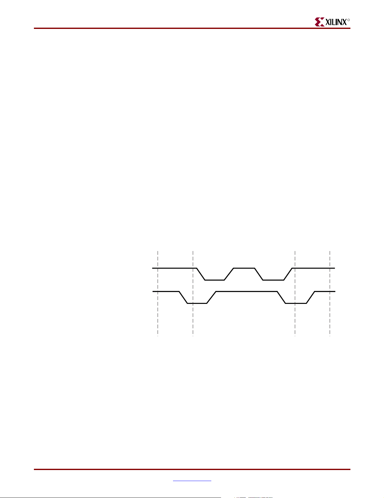
start or stop bit condition as shown in Figure 2-6. A high-to-low transition of
SDRAM_SDA when SDRAM_SCL is high indicates a start bit condition, the start of all
commands. A low-to-high transition of SDRAM_SDA when SDRAM_ SCL is high
indicates a stop bit condition, terminating the command placing the SPD device into a low
power mode.
2
C bus protocol using the SDRAM_SCL (serial
R
SDRAM_SCL
SDRAM_SDA
START BIT STOP BIT
UG069_07_082604
Figure 2-6: Definition of Start and Stop Conditions
All commands commence with a start bit, followed by eight data bits. The transmitting
device, either the bus master or slave, releases the bus after transmitting eight bits. During
the ninth clock cycle, the receiver pulses the SDA data signal low to acknowledge that it
received the eight bits of data as shown in Figure 2-7.
XUP Virtex-II Pro Development System www.xilinx.com 25
UG069 (v1.0) March 8, 2005
Page 26
R
SCL FROM
MASTER
SDA OUTPUT FROM
TRANSMITTER
SDA OUTPUT FROM
RECEIVER
Chapter 2: Using the System
1289
START BIT ACKNOWLEDGE
UG069_08_021405
Figure 2-7: Acknowledge Response from Receiver
The SPD device always responds with an acknowledge after recognition of a start
condition and its slave address (100). If a read command was issued, the SPD device
transmits eight bits of data, releases the SDRAM_SDA data line, and monitors the
SDRAM_SDA data line for an acknowledge. If an acknowledge is detected and no stop bit is
generated by the master, the SPD device continues to transmit data. If no acknowledge is
detected, the SPD device terminates further data transmission and waits for the stop bit
condition to return to low power mode.
MASTER
(FPGA)
SDRAM_SDA
SLAVE
(SPD EEPROM)
MASTER
(FPGA)
SDRAM_SDA
SPD device read and write operations are shown in Figure 2-8 and Figure 2-9.
SLAVE ADDRESS
READ DATA n DATA n+1
START
0011 00011
A2A1A0
R/W
ACK
ACK
Figure 2-8: EEPROM Sequential Read
SLAVE ADDRESS
WRITE WORD ADDRESS DATA
START
0011 00011
A2
A1A0R/W
ACK
STOP
UG069_09_021405
STOP
SLAVE
(SPD EEPROM)
ACK
ACK
ACK
UG069_10_021405
Figure 2-9: EEPROM Write
26 www.xilinx.com XUP Virtex-II Pro Development System
UG069 (v1.0) March 8, 2005
Page 27
Using the DIMM Module DDR SDRAM
The ability to read the SPD EEPROM is important because the module specific timing
parameters are included in the EEPROM data and are required by the DDR SDRAM
controller to provide the highest memory throughput. The definitions of the SPD data
bytes are outlined in Tab le 2 -3.
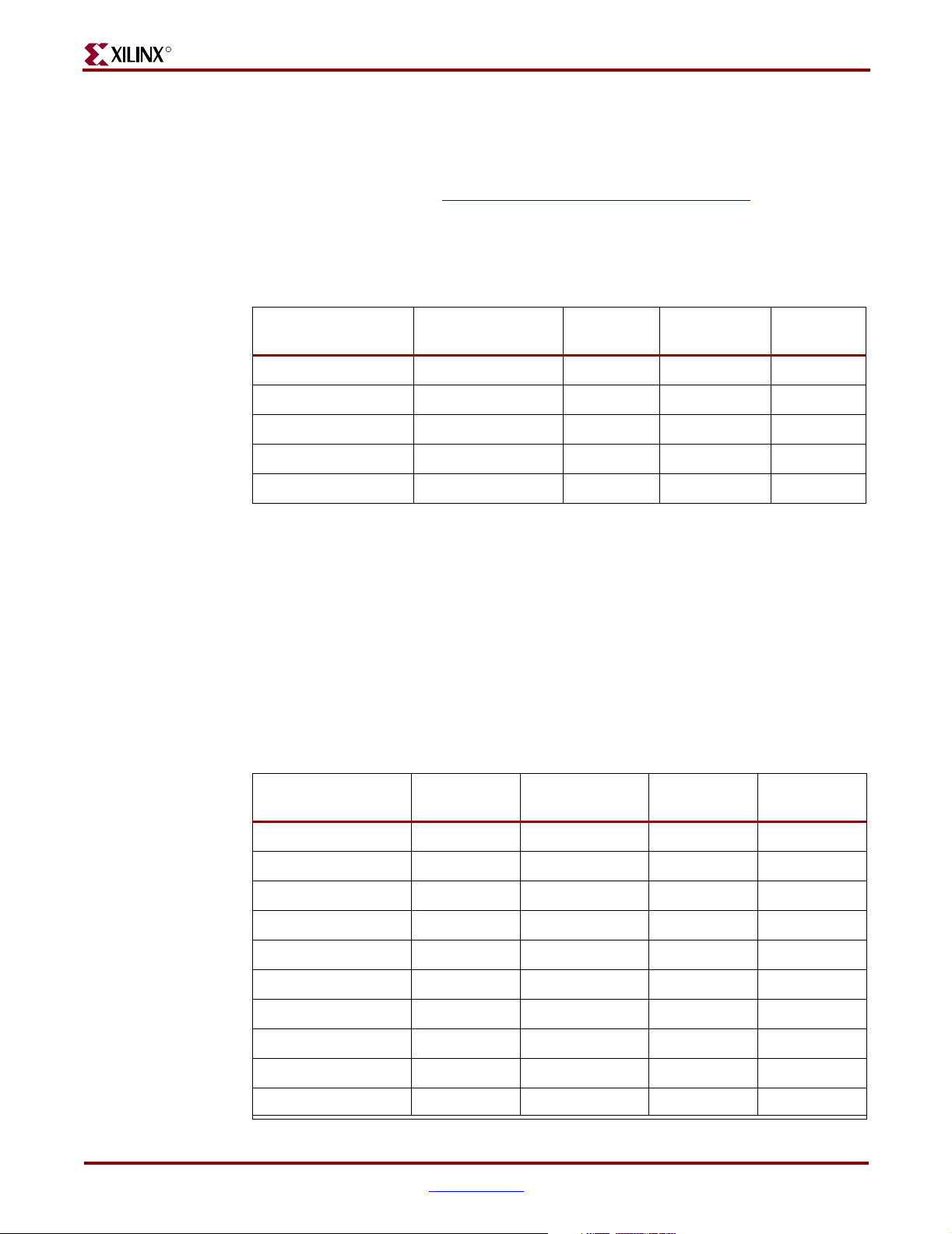
Table 2-3: SPD EEPROM Contents
Byte Description
0 Number of used bytes in SPD EEPROM
1 Total number of bytes on SPD EEPROM
2 Memory type (DDR SDRAM = 07h)
3Number of row addresses
4 Number of column addresses
5 Number of ranks (01h)
6-7 Module data width
8 Module interface voltage (SSTL 2.5V = 04h)
R
9 SDRAM cycle time (tck) (CAS LATENCY = 2.5)
10 SDRAM access time (tac) (CAS LATENCY = 2.5)
11 Module configuration type
12 Refresh rate
13 Primary SDRAM component width
14 Error checking SDRAM component width
15 Minimum clock delay from
Back-to-Back Random Column Addresses
16 Supported burst lengths
17 Number of banks on SDRAM component
18 CAS latencies supported
19 CS latency
20 WE latency
21 SDRAM module attributes
22 SDRAM attributes
23 SDRAM cycle time (tck) (CAS LATENCY =2)
24 SDRAM access time (tac) (CAS LATENCY =2)
25 SDRAM cycle time (tck) (CAS LATENCY =1)
26 SDRAM access time (tac) (CAS LATENCY =1)
27 Minimum ROW PRECHARGE time (trp)
28 Minimum ROW ACTIVE to ROW ACTIVE (trrd)
XUP Virtex-II Pro Development System www.xilinx.com 27
UG069 (v1.0) March 8, 2005
Page 28
R
Chapter 2: Using the System
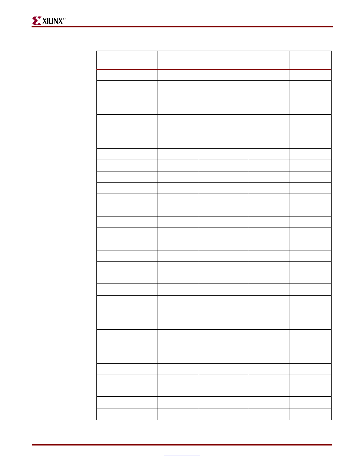
Table 2-3: SPD EEPROM Contents (Continued)
Byte Description
29 Minimum RAS# to CAS# delay (trcd)
30 Minimum RAS# pulse width (tras)
31 Module rank density
32 Command and address setup time (tas, tcms)
33 Command and address hold time (tah, tcmh)
34 Data setup time (tds)
35 Data hold time (tdh)
36-40 Reserved
41 Minimum ACTIVE/AUTO REFRESH time
42 Minimum AUTO REFRESH to ACTIVE/AUTO REFRESH
command period
43 Max cycle time
44 Max DQS-DQ skew
45 Max READ HOLD time
46 Reserved
47 DIMM height
48-61 Reserved
62 SPD revision
63 CHECKSUM for bytes 0-62
64-71 Manufacturer's JEDEC ID code
72 Manufacturing location
73-90 Module part number (ASCII)
91-92 Module revision code
93 Year of manufacture (BCD)
94 Week of manufacturer (BCD)
95-98 Module serial number
99-127 Reserved
128-255 User defined contents
The DIMM module is supplied with three differential clocks. These three clock signals are
matched in length to each other and the DDR SDRAM feedback signals to allow for fully
synchronous operation across all banks of memory. The DDR SDRAM clocks are driven by
Double Data Rate (DDR) output registers, connected to a Digital Clock Manager (DCM)
with an optional external feedback connection. The DDR SDRAM controller logic is
described in DS425
28 www.xilinx.com XUP Virtex-II Pro Development System
, PLB Double Data Rate (DDR) Synchronous DRAM (SDRAM) Controller.
UG069 (v1.0) March 8, 2005
Page 29
Using the DIMM Module DDR SDRAM
The Xilinx PLB DDR SDRAM controller is a soft IP core designed for Xilinx FPGAs that
support different CAS latencies and memory data widths set by design parameters.
The DDR SDRAM controller logic instantiates DDR input and output registers on the
address, data, and control signals, so the clock to output delays match the clock output
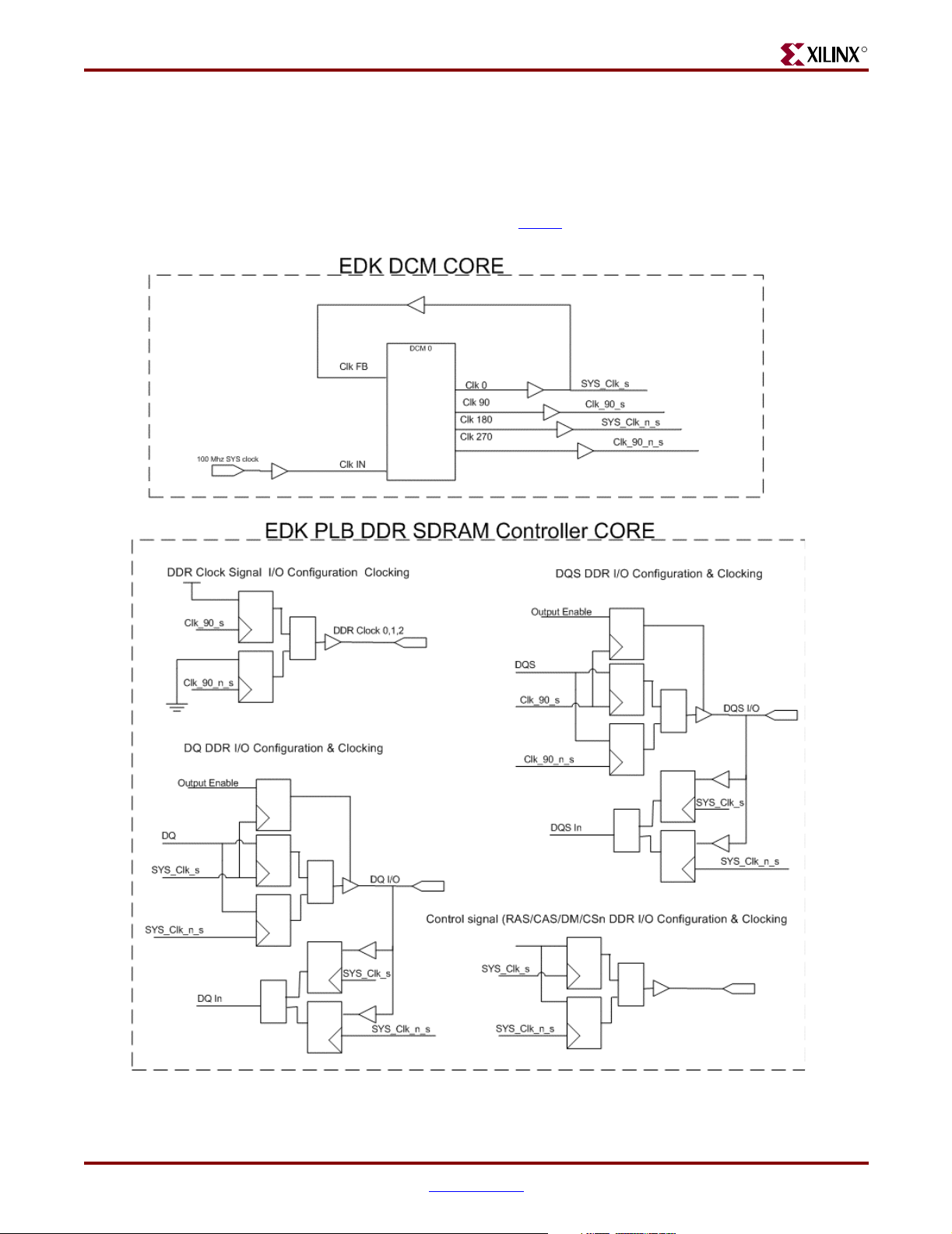
delay. The DDR SDRAM clocking structure as shown in Figure 2-10 is a simplified version
of the clocking structure mentioned in DS425
R
.
ug069_23_021505
Figure 2-10: Clock Generation for the DDR SDRAM
XUP Virtex-II Pro Development System www.xilinx.com 29
UG069 (v1.0) March 8, 2005
Page 30
R
Chapter 2: Using the System
Xilinx has qualified several different types of PC2100 memory modules for use in the XUP
Virtex-II Pro Development System. These modules cover various densities, organizations,
and features. The qualified memory modules are identified in Ta bl e 2-4 .
For an updated list of supported modules, consult the XUP Virtex-II Pro Development
System support Web site at:
http://www.xilinx.com/univ/xupv2p.html
The data bus width, number of ranks, address range, clock latency, and output type are all
parameters that are used by the DDR memory controller design to create the correct
memory controller for the user application.
Table 2-4: Qualified SDRAM Memory Modules
Crucial® Technology
Part Number
Memory
Organization
Number of
Ranks
Unbuffered or
Registered
CAS
Latency
CT6472Z265.18T* 512 MB 64M X 72 Dual Unbuffered 2.5
CT6464Z265.16T* 512 MB 64M X 64 Dual Unbuffered 2.5
CT6472Z265.9T* 512 MB 64M X 72 Single Unbuffered 2.5
CT6464Z265.8T* 512 MB 64M X 64 Single Unbuffered 2.5
CT1664Z265.4T* 128 MB 16M X 64 Single Unbuffered 2.5
Notes:
The * in the Crucial part number represents the revision number of the module, which is not
required to order the module.
These memory modules are designed for a maximum clock frequency of at least 133 MHz
and have a CAS latency of 2.5 (18.8 ns). The PLB Double Data Rate Synchronous DRAM
Controller supports CAS latencies of two or three clock cycles.
If the memory system is to operate at 100 MHz, then set the CAS latency parameter in the
controller design to 2 (20 ns). If full speed (133MHz) memory operation is required, then
set the CAS latency parameter in the controller design to 3 (22.6 ns).
Tab le 2 -5 provides the details on the FPGA to DDR SDRAM DIMM module connections.
Table 2-5: DDR SDRAM Connections
Signal Direction
DIMM
Module Pin
FPGA
Pin
I/O Type
SDRAM_DQ[0] I/O 2 C27 SSTL2-II
SDRAM_DQ[1] I/O 4 D28 SSTL2-II
SDRAM_DQ[2] I/O 6 D29 SSTL2-II
SDRAM_DQ[3] I/O 8 D30 SSTL2-II
SDRAM_DQ[4] I/O 94 H25 SSTL2-II
SDRAM_DQ[5] I/O 95 H26 SSTL2-II
SDRAM_DQ[6] I/O 98 E27 SSTL2-II
SDRAM_DQ[7] I/O 99 E28 SSTL2-II
SDRAM_DQS[0] I/O 5 E30 SSTL2-II
SDRAM_DM[0] 0 97 U26 SSTL2-II
30 www.xilinx.com XUP Virtex-II Pro Development System
UG069 (v1.0) March 8, 2005
Page 31

Using the DIMM Module DDR SDRAM
Table 2-5: DDR SDRAM Connections (Continued)
R
Signal Direction
DIMM
Module Pin
FPGA
Pin
I/O Type
SDRAM_DQ[8] I/O 12 J26 SSTL2-II
SDRAM_DQ[9] I/O 13 G27 SSTL2-II
SDRAM_DQ[10] I/O 19 G28 SSTL2-II
SDRAM_DQ[11] I/O 20 G30 SSTL2-II
SDRAM_DQ[12] I/O 105 L23 SSTL2-II
SDRAM_DQ[13] I/O 106 L24 SSTL2-II
SDRAM_DQ[14] I/O 109 H27 SSTL2-II
SDRAM_DQ[15] I/O 110 H28 SSTL2-II
SDRAM_DQS[1] I/O 14 J29 SSTL2-II
SDRAM_DM[1] 0 107 V29 SSTL2-II
SDRAM_DQ[16] I/O 23 J27 SSTL2-II
SDRAM_DQ[17] I/O 24 J28 SSTL2-II
SDRAM_DQ[18] I/O 28 K29 SSTL2-II
SDRAM_DQ[19] I/O 31 L29 SSTL2-II
SDRAM_DQ[20] I/O 114 N23 SSTL2-II
SDRAM_DQ[21] I/O 117 N24 SSTL2-II
SDRAM_DQ[22] I/O 121 K27 SSTL2-II
SDRAM_DQ[23] I/O 123 K28 SSTL2-II
SDRAM_DQS[2] I/O 25 M30 SSTL2-II
SDRAM_DM[2] 0 119 W29 SSTL2-II
SDRAM_DQ[24] I/O 33 R22 SSTL2-II
SDRAM_DQ[25] I/O 35 M27 SSTL2-II
SDRAM_DQ[26] I/O 39 M28 SSTL2-II
SDRAM_DQ[27] I/O 40 P30 SSTL2-II
SDRAM_DQ[28] I/O 126 P23 SSTL2-II
SDRAM_DQ[29] I/O 127 P24 SSTL2-II
SDRAM_DQ[30] I/O 131 N27 SSTL2-II
SDRAM_DQ[31] I/O 133 N28 SSTL2-II
SDRAM_DQS[3] I/O 36 P29 SSTL2-II
SDRAM_DM[3] 0 129 T22 SSTL2-II
SDRAM_DQ[32] I/O 53 V27 SSTL2-II
XUP Virtex-II Pro Development System www.xilinx.com 31
UG069 (v1.0) March 8, 2005
Page 32
R
Chapter 2: Using the System
Table 2-5: DDR SDRAM Connections (Continued)
Signal Direction
DIMM
Module Pin
FPGA
Pin
I/O Type
SDRAM_DQ[33] I/O 55 Y30 SSTL2-II
SDRAM_DQ[34] I/O 57 U24 SSTL2-II
SDRAM_DQ[35] I/O 60 U23 SSTL2-II
SDRAM_DQ[36] I/O 146 V26 SSTL2-II
SDRAM_DQ[37] I/O 147 V25 SSTL2-II
SDRAM_DQ[38] I/O 150 Y29 SSTL2-II
SDRAM_DQ[39] I/O 151 AA29 SSTL2-II
SDRAM_DQS[4] I/O 56 V23 SSTL2-II
SDRAM_DM[4] 0 149 W28 SSTL2-II
SDRAM_DQ[40] I/O 61 Y26 SSTL2-II
SDRAM_DQ[41] I/O 64 AA28 SSTL2-II
SDRAM_DQ[42] I/O 68 AA27 SSTL2-II
SDRAM_DQ[43] I/O 69 W24 SSTL2-II
SDRAM_DQ[44] I/O 153 W23 SSTL2-II
SDRAM_DQ[45] I/O 155 AB28 SSTL2-II
SDRAM_DQ[46] I/O 161 AB27 SSTL2-II
SDRAM_DQ[47] I/O 162 AC29 SSTL2-II
SDRAM_DQS[5] I/O 67 AA25 SSTL2-II
SDRAM_DM[5] 0 159 W27 SSTL2-II
SDRAM_DQ[48] I/O 72 AB25 SSTL2-II
SDRAM_DQ[49] I/O 73 AE29 SSTL2-II
SDRAM_DQ[50] I/O 79 AA24 SSTL2-II
SDRAM_DQ[51] I/O 80 AA23 SSTL2-II
SDRAM_DQ[52] I/O 165 AD28 SSTL2-II
SDRAM_DQ[53] I/O 166 AD27 SSTL2-II
SDRAM_DQ[54] I/O 170 AF30 SSTL2-II
SDRAM_DQ[55] I/O 171 AF29 SSTL2-II
SDRAM_DQS[6] I/O 78 AC25 SSTL2-II
SDRAM_DM[6] 0 169 W26 SSTL2-II
SDRAM_DQ[56] I/O 83 AF25 SSTL2-II
SDRAM_DQ[57] I/O 84 AG30 SSTL2-II
32 www.xilinx.com XUP Virtex-II Pro Development System
UG069 (v1.0) March 8, 2005
Page 33

Using the DIMM Module DDR SDRAM
Table 2-5: DDR SDRAM Connections (Continued)
R
Signal Direction
DIMM
Module Pin
FPGA
Pin
I/O Type
SDRAM_DQ[58] I/O 87 AG29 SSTL2-II
SDRAM_DQ[59] I/O 88 AD26 SSTL2-II
SDRAM_DQ[60] I/O 174 AD25 SSTL2-II
SDRAM_DQ[61] I/O 175 AG28 SSTL2-II
SDRAM_DQ[62] I/O 178 AH27 SSTL2-II
SDRAM_DQ[63] I/O 179 AH29 SSTL2-II
SDRAM_DQS[7] I/O 86 AH26 SSTL2-II
SDRAM_DM[7] 0 177 W25 SSTL2-II
SDRAM_CB[0] I/O 44 R28 SSTL2-II
SDRAM_CB[1] I/O 45 U30 SSTL2-II
SDRAM_CB[2] I/O 49 V30 SSTL2-II
SDRAM_CB[3] I/O 51 T26 SSTL2-II
SDRAM_CB[4] I/O 134 T25 SSTL2-II
SDRAM_CB[5] I/O 135 T28 SSTL2-II
SDRAM_CB[6] I/O 142 T27 SSTL2-II
SDRAM_CB[7] I/O 144 U28 SSTL2-II
SDRAM_DQS[8] I/O 47 T23 SSTL2-II
SDRAM_DM[8] 0 140 U22 SSTL2-II
SDRAM_A[0] O 48 M25 SSTL2-II
SDRAM_A[1] O 43 N25 SSTL2-II
SDRAM_A[2] O 41 L26 SSTL2-II
SDRAM_A[3] O 130 M29 SSTL2-II
SDRAM_A[4] O 37 K30 SSTL2-II
SDRAM_A[5] O 32 G25 SSTL2-II
SDRAM_A[6] O 125 G26 SSTL2-II
SDRAM_A[7] O 29 D26 SSTL2-II
SDRAM_A[8] O 122 J24 SSTL2-II
SDRAM_A[9] O 27 K24 SSTL2-II
SDRAM_A[10] O 141 F28 SSTL2-II
SDRAM_A[11] O 118 F30 SSTL2-II
SDRAM_A[12] O 115 M24 SSTL2-II
XUP Virtex-II Pro Development System www.xilinx.com 33
UG069 (v1.0) March 8, 2005
Page 34
R
Chapter 2: Using the System
Table 2-5: DDR SDRAM Connections (Continued)
Signal Direction
DIMM
Module Pin
FPGA
Pin
I/O Type
SDRAM_A[13] O 167 M23 SSTL2-II
SDRAM_CK0 O 137 AC27 SSTL2-II
SDRAM_CK0_Z O 138 AC28 SSTL2-II
SDRAM_CK1 O 16 AD29 SSTL2-II
SDRAM_CK1_Z O 17 AD30 SSTL2-II
SDRAM_CK2 O 76 AB23 SSTL2-II
SDRAM_CK2_Z O 75 AB24 SSTL2-II
CLK_FEEDBACK O – G23 LVCMOS25
CLK_FEEDBACK I – C16 LVCMOS25
SDRAM_CKE0 O 21 R26 SSTL2-II
SDRAM_CKE1 O 111 R25 SSTL2-II
SDRAM_RAS_Z O 154 N29 SSTL2-II
SDRAM_CAS_Z O 65 L27 SSTL2-II
SDRAM_WE_Z O 63 N26 SSTL2-II
SDRAM_S0_Z O 157 R24 SSTL2-II
SDRAM_S1_Z O 158 R23 SSTL2-II
SDRAM_BA0 O 59 M26 SSTL2-II
SDRAM_BA1 O 52 K26 SSTL2-II
SDRAM_SDA I/O 91 AF23 LVCMOS25
SDRAM_SCL O 92 AF22 LVCMOS25
SDRAM_SA0 NA 181 – NA
SDRAM_SA1 NA 182 – NA
SDRAM_SA2 NA 183 – NA
Using the XSGA Output
The XSGA output on the XUP Virtex-II Pro Development System is made up from a triple
8-bit DAC (U29), a high density 15-pin D-Sub connector (J13), and IP placed in the FPGA
fabric. The FMS3818 video DAC is a low-cost DAC tailored to fit graphics and video
applications, with a maximum pixel clock of 180 MHz. The TTL data inputs and control
signals are converted into analog current outputs that can drive 25Ω to 37.5Ω loads,
corresponding to a doubly-terminated 50Ω to 75Ω load. The VGA_OUT_BLANK_Z input
overrides the RGB inputs and blanks the display output. This signal is equipped with a
pull-down resistor (R120) to keep the display blanked when the FPGA is not programmed
or XSGA output is not required by the user application. The XSGA output circuit is shown
in Figure 2-11.
34 www.xilinx.com XUP Virtex-II Pro Development System
UG069 (v1.0) March 8, 2005
Page 35

Using the XSGA Output
R
Design files supplied by Xilinx generate the required timing signals
VGA_OUT_BLANK_Z, VGA_HSYNCH, VGA_VSYNCH, and VGA_COMP_SYNCH, as
well as memory addressing for bit- and character-mapped display RAM. Charactermapped mode allows for the display of extended ASCII characters in an 8 x 8 pixel block
without having to draw the character pixel by pixel. Compile time parameters are passed
to the Verilog code that defines the XSGA controller operation. The 100 MHz clock is used
as a source for one of the DCMs to create the video clock. By setting appropriate M and D
values for the DCM, various VGA_OUT_PIXEL_CLOCK rates can be created.
XUP Virtex-II Pro Development System www.xilinx.com 35
UG069 (v1.0) March 8, 2005
Page 36

R
J13
123456789
VGA OUTPUT
VGA_RED_OUT
VGA_GREEN_OUT
VGA_BLUE_OUT
R116
1011121314
R117
82R5 1%
15
HD-15PIN VGA DSUB
VGA_GND
82R5 1%
Chapter 2: Using the System
UG069_12_101804
VGA_GND
R115
R114
R113
VGA_HSYNCH
75R0 1%
75R0 1%
75R0 1%
33
IOR
U29
R0R1R2R3R4R5R6R7G0G1G2G3G4G5G6G7B0B1B2B3B4B5B6
40
41424344454647
VGA_VSYNCH
32
IOG
2345678
29
IOB
9
16171819202122
VGA_VCC
C458
VGA_GND
0.1UF
C457
0.1UF
R119
348.1%
GND1
GND2
GND3
GND4
VAA1
VAA2NCNCNCNC
GND5
GND6
39382827151448
R120
GND7
3K3
TRIPLE 8 BIT
VIDEO DAC
FMS3818KRC
GND
1
36
35
34
RSET
CLOCK
VGA_VCC
GND0
VDD
31123013242537
COMP
VREF
BLANK
SYNC
B7
23
11
10
VGA_OUT_RED0
VGA_OUT_RED1
VGA_OUT_RED2
VGA_OUT_RED3
VGA_OUT_RED4
VGA_OUT_RED5
VGA_OUT_RED6
VGA_OUT_RED7
VGA_OUT_GREEN0
VGA_OUT_GREEN1
VGA_OUT_GREEN2
VGA_OUT_GREEN3
VGA_OUT_BLUE0
VGA_OUT_GREEN4
VGA_OUT_BLUE1
VGA_OUT_GREEN5
VGA_OUT_GREEN6
VGA_OUT_GREEN7
VGA_OUT_BLUE2
VGA_OUT_BLUE3
VGA_OUT_BLUE4
VGA_OUT_BLUE5
VGA_OUT_BLUE6
VGA_OUT_BLUE7
VGA_COMP_SYNCH
VGA_OUT_BLANK_Z
R118
20R0 1%
VGA_OUT_PIXEL_CLOCK
Figure 2-11: XSGA Output
36 www.xilinx.com XUP Virtex-II Pro Development System
UG069 (v1.0) March 8, 2005
Page 37

Using the XSGA Output
R
Tab le 2 -6 lists the Verilog parameter values and the DCM settings for various XSGA output
formats.
Note:
The highlighted settings are exact VESA settings; the others are approximations.
Table 2-6: DCM and XSGA Controller Settings for Various XSGA Formats
Verilog Horizontal Timing Parameters
Output
Format
Pixel
Clock
DCM
Settings
H Active H FP H Synch H BP H Total
MHz M D Pixels Pixels Pixels Pixels Pixels
640 x 480 @ 60 Hz 25.00 1 4 640 16 96 48 800
640 x 480 @ 72 Hz 31.25 5 16 640 24 40 128 832
640 x 480 @ 75 Hz 31.25 5 16 640 18 96 42 796
640 x 480 @ 85 Hz 35.71 5 14 640 32 48 108 828
800 x 600 @ 60 Hz 40.00 4 10 800 40 128 88 1056
800 x 600 @ 72 Hz 50.00 1 2 800 56 120 64 1040
800 x 600 @ 75 Hz 50.00 1 2 800 16 80 168 1064
800 x 600 @ 85 Hz 55.00 11 20 800 32 64 144 1040
1024 x 768 @ 60 Hz 65.00 13 20 1024 24 136 160 1344
1024 x 768 @ 72 Hz 75.00 15 20 1024 16 96 172 1308
1024 x 768 @ 75 Hz 80.00 8 10 1024 24 96 184 1328
1024 x 768 @ 85 Hz 95.00 19 20 1024 48 96 208 1376
1280 x 1024 @ 60 Hz 110.00 11 10 1280 52 120 256 1708
1280 x 1024 @ 72 Hz 130.00 13 10 1280 16 144 248 1688
1280 x 1024 @ 75 Hz 135.00 27 20 1280 16 144 248 1688
1280 x 1024 @ 85 Hz 150.00 3 2 1280 40 144 224 1688
1200 x 1600 @ 60 Hz 160.00 16 10 1600 56 192 296 2144
1200 x 1600 @ 70 Hz 180.00 18 10 1600 40 184 256 2080
Verilog Vertical Timing Parameters
Output
Format
Pixel
Clock
DCM
Settings
V Active V FP V Synch V BP V Total
MHz M D Pixels Pixels Pixels Pixels Pixels
640 x 480 @ 60 Hz 25.00 1 4 480 9 2 29 520
640 x 480 @ 72 Hz 31.25 5 16 480 10 3 29 522
640 x 480 @ 75 Hz 31.25 5 16 480 11 2 31 524
640 x 480 @ 85 Hz 35.71 5 14 480 1 3 23 507
800 x 600 @ 60 Hz 40.00 4 10 600 1 4 23 628
800 x 600 @ 72 Hz 50.00 1 2 600 37 6 23 666
XUP Virtex-II Pro Development System www.xilinx.com 37
UG069 (v1.0) March 8, 2005
Page 38
R
Chapter 2: Using the System
Table 2-6: DCM and XSGA Controller Settings for Various XSGA Formats (Continued)
Verilog Horizontal Timing Parameters
Output
Format
Pixel
Clock
DCM
Settings
H Active H FP H Synch H BP H Total
MHz M D Pixels Pixels Pixels Pixels Pixels
800 x 600 @ 75 Hz 50.00 1 2 600 1 2 23 626
800 x 600 @ 85 Hz 55.00 11 20 600 1 3 18 622
1024 x 768 @ 60 Hz 65.00 13 20 768 3 6 29 806
1024 x 768 @ 72 Hz 75.00 15 20 768 1 3 24 796
1024 x 768 @ 75 Hz 80.00 8 10 768 2 4 29 803
1024 x 768 @ 85 Hz 95.00 19 20 768 2 4 38 812
1280 x 1024 @ 60 Hz 110.00 11 10 1024 3 5 42 1074
1280 x 1024 @ 72 Hz 130.00 13 10 1024 2 4 40 1070
1280 x 1024 @ 75 Hz 135.00 27 20 1024 1 3 38 1066
1280 x 1024 @ 85 Hz 150.00 3 2 1024 1 3 28 1056
1200 x 1600 @ 60 Hz 160.00 16 10 1200 1 3 40 1244
1200 x 1600 @ 70 Hz 180.00 18 10 1200 1 3 38 1242
The connections between the FPGA and the XSGA output DAC and connector are listed in
Tab le 2 -7 along with the required I/O characteristics.
Table 2-7: XSGA Output Connections
Signal Direction
Video
DAC or Output
Connector Pin
FPGA
Pin
I/O Type Drive Slew
VGA_OUT_RED[0] O 40 G8 LVTTL 8 mA SLOW
VGA_OUT_RED[1] O 41 H9 LVTTL 8 mA SLOW
VGA_OUT_RED[2] O 42 G9 LVTTL 8 mA SLOW
VGA_OUT_RED[3] O 43 F9 LVTTL 8 mA SLOW
VGA_OUT_RED[4] O 44 F10 LVTTL 8 mA SLOW
VGA_OUT_RED[5] O 45 D7 LVTTL 8 mA SLOW
VGA_OUT_RED[6] O 46 C7 LVTTL 8 mA SLOW
VGA_OUT_RED[7] O 47 H10 LVTTL 8 mA SLOW
VGA_OUT_GREEN[0] O 2 G10 LVTTL 8 mA SLOW
VGA_OUT_GREEN[1] O 3 E10 LVTTL 8 mA SLOW
VGA_OUT_GREEN[2] O 4 D10 LVTTL 8 mA SLOW
VGA_OUT_GREEN[3] O 5 D8 LVTTL 8 mA SLOW
VGA_OUT_GREEN[4] O 6 C8 LVTTL 8 mA SLOW
38 www.xilinx.com XUP Virtex-II Pro Development System
UG069 (v1.0) March 8, 2005
Page 39

Using the AC97 Audio CODEC and Power Amp
Table 2-7: XSGA Output Connections (Continued)
R
Signal Direction
Video
DAC or Output
Connector Pin
FPGA
Pin
I/O Type Drive Slew
VGA_OUT_GREEN[5] O 7 H11 LVTTL 8 mA SLOW
VGA_OUT_GREEN[6] O 8 G11 LVTTL 8 mA SLOW
VGA_OUT_GREEN[7] O 9 E11 LVTTL 8 mA SLOW
VGA_OUT_BLUE[0] O 16 D15 LVTTL 8 mA SLOW
VGA_OUT_BLUE[1] O 17 E15 LVTTL 8 mA SLOW
VGA_OUT_BLUE[2] O 18 H15 LVTTL 8 mA SLOW
VGA_OUT_BLUE[3] O 19 J15 LVTTL 8 mA SLOW
VGA_OUT_BLUE[4] O 20 C13 LVTTL 8 mA SLOW
VGA_OUT_BLUE[5] O 21 D13 LVTTL 8 mA SLOW
VGA_OUT_BLUE[6] O 22 D14 LVTTL 8 mA SLOW
VGA_OUT_BLUE[7] O 23 E14 LVTTL 8 mA SLOW
VGA_OUT_PIXEL_CLOCK O 26 H12 LVTTL 12 mA SLOW
VGA_COMP_SYNCH O 11 G12 LVTTL 12 mA SLOW
VGA_OUT_BLANK_Z O 10 A8 LVTTL 12 mA SLOW
VGA_HSYNCH O J13.14 B8 LVTTL 12 mA SLOW
VGA_VSYNCH O J13.13 D11 LVTTL 12 mA SLOW
Using the AC97 Audio CODEC and Power Amp
The audio system on the XUP Virtex-II Pro Development System consists of a National
Semiconductor® LM4550 AC97 audio CODEC paired with a stereo power amplifier
(TPA6111A) made by Texas Instruments. The AC97-compliant audio CODEC is widely
used as the audio system in PCs and MACs, ensuring availability of drivers for these
devices.
The LM4550 audio CODEC supports the following features:
• Greater than 90 dB dynamic range
• 18-bit Σ∆ converter architecture
• 18-bit full-duplex, stereo CODEC
• Four analog line-level stereo inputs (one is used on the XUP Virtex-II Pro
Development System)
• Two analog line-level stereo outputs
• Mono MIC input with built-in 20 dB preamp, selectable for two sources (one used)
• VREF_OUT, reference voltage provides bias current for Electret microphones
• Power management support
• Full-duplex variable sample rates from 4 kHz to 48 kHz in 1 Hz increments
XUP Virtex-II Pro Development System www.xilinx.com 39
UG069 (v1.0) March 8, 2005
Page 40

R
Chapter 2: Using the System
• Independently adjustable input volume controls with mute and a maximum gain of
12 dB and attenuation of 34.5 dB in 1.5 dB steps
• 3D stereo enhancement
• PC Beep tone input passthrough to Line Out
The TPA6111A audio power amplifier supports the following features:
• Fixed Gain
• Stereo Power Amplifier delivers 150 mW per channel into 16Ω
• Click and Pop suppression
The National Semiconductor LM4550 uses 18-bit Sigma-Delta A/Ds and D/As, providing
90 dB of dynamic range. The implementation on this board, shown in Figure 2-12, allows
for full-duplex stereo A/D and D/A with one stereo input and two mono inputs, each of
which has separate gain, attenuation, and mute control. The mono inputs are a
microphone input with 2.2V bias and a beep tone input from the FPGA. The
BEEP_TONE_IN (TTL level) is applied to both outputs, even if the CODEC is held in reset
to allow test tones to be heard. The CODEC has two stereo line-level outputs with
independent volume controls. One of the line-level outputs drives the audio output
connector and the second line-level output drives the on-board power amplifier shown in
Figure 2-13.
The power amplifier is capable of producing 150 mW of continuous power per channel
into 16Ω loads, such as headphones. The assertion of the AUDIO_AMP_SHUTDOWN
signal by the CODEC causes the audio power amplifier to turn off.
The TPA6111A audio power amplifier contains circuitry to minimize turn-on transients,
that is, click or pops. Tu rn - o n refers to either power supply turn-on or the device coming out
of CODEC controlled shutdown. When the device is turning on, the amplifiers are
internally muted until the bypass pin has reached half the supply voltage. The turn-on
time is controlled by C9.
The power amplifier was included to support two output modes, line out mode and power
amp output mode. The line level output attenuation is controlled by the CODEC volume
control register 04h, and the power amp output attenuation is controlled by CODEC
volume control register 02h.
40 www.xilinx.com XUP Virtex-II Pro Development System
UG069 (v1.0) March 8, 2005
Page 41
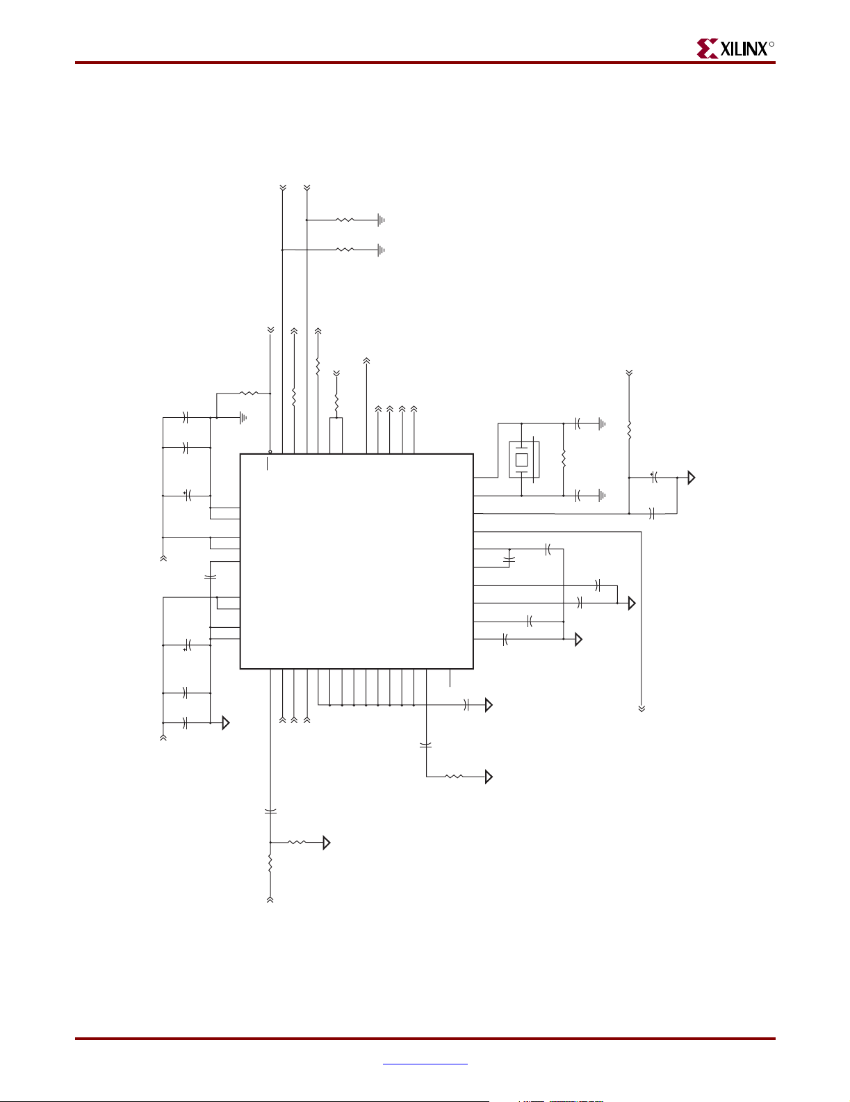
Using the AC97 Audio CODEC and Power Amp
AC97_SDATA_OUT
AC97_SYNCH
R170
3K3
R169
3K3
AUDIO_RESET_Z
AC97_SDATA_IN
AC97_BIT_CLOCK
R
UG069_14_101804
VCC3V3
AUDIO_5V
C31C30C29
10UF 16V
C28C27C26
0.1UF 0.1UF
C32
10UF 16V
0.1UF0.1UF
7
4
9
1
40
1UF
43
44
38
25
42
26
AUDIO_GND
VCC3V3
R15
3K3
GND
DVSS1
DVSS0
DVDD1
DVDD0
NC2
NC1
NC0
AVDD1
AVDD0
AVSS1
AVSS0
12242321222019181716151413
BEEP_TONE
C33
R167 56R2 1%
RESET
SDATA_IN
SDATA_OUT
U9
PC_BEEP
LINE_IN_R
LINE_IN_L
AUDIO_LINE_IN_LEFT
AUDIO_LINE_IN_RIGHT
1UF
R168 56R2 1%
R18
10K
46
45
6108511
CS0
CS1
SYNCH
BIT_CLOCK
AC97 CODEC
AUDIO MIXER AND CODEC
MIC1
MIC2
CD_4
CD_GND
CD_L
MIC_IN
AUDIO_AMP_SHUTDOWN
AUDIO_LINE_OUT_LEFT
AUDIO_LINE_OUT_RIGHT
47
413938
LNLVL_OUT_L
LNLVL_OUT_R
AMP_PWR_DWN
VIDEO_R
VIDEO_L
AUX_R
AUDIO_RIGHT
AUDIO_LEFT
35
LINE_OUT_L
LINE_OUT_R
AUX_L
PHONE_IN
37
MONO
C34
MONO_OUT
48
1UF
R19
SPDIF
47K
XTAL_OUT
XTAL_IN
VREF
VREF_OUT
RX3D
CX3D
FILT_R
FILT_L
AFLT2
AFILT1
0.1UF
C35
3
2
27
28
33
C37
34
32
31
30
29
AUDIO_GND
AUDIO_GND
AUDIO_5V
R21
10K
Y1
100NF
C38
270PF
C36
C39
270PF
24.576 MHz
R20
47NF
1M0
22PF 22PF
C43
C40 C41 C42
AUDIO_GND
GND GND
1UF
1UF
AUDIO_GND
MIC_POWER
C45
C44
10UF 16V
100NF
AUDIO_GND
R17
4K7
AUDIO_GND
R16
6K8
BEEP_TONE_IN
Figure 2-12: AC97 Audio CODEC
XUP Virtex-II Pro Development System www.xilinx.com 41
UG069 (v1.0) March 8, 2005
Page 42

R
Chapter 2: Using the System
UPPER
J14B
HZ0805E601R-00
HZ0805E601R-00
L1
L2
22OUF 10V
22OUF 10V
C1
C3
AMP_OUT_LEFT
AMP_OUT_RIGHT
UPPER
MIC_IN
DUAL_STEREO_JACK
J15B
DUAL_STEREO_JACK
MIC_POWER
UG069_13_101804
1UF
HZ0805E601R-00
HZ0805E601R-00
470PF
C13
L4
L3
R3
47K
470PF 470PF
C6 C7
R2
47K
AUDIO_GND AUDIO_GND AUDIO_GND AUDIO_GND AUDIO_GND
1UF
C10
R7
47K
470PF
C12
R6
47K
1UF
C11
AUDIO_LINE_OUT_LEFT
AUDIO_LINE_OUT_RIGHT
AUDIO_GND AUDIO_GND AUDIO_GND AUDIO_GND
AUDIO_GND
2K0
R10
47K
R12
HZ0805E601R-00
HZ0805E601R-00
L6
L8
J14A
LOWER
C18
C21 C22 C23
DUAL_STEREO_JACK
AUDIO_GND
470PF 0.1UF
470PF
AUDIO_GND AUDIO_GND
AUDIO_GND
AUDIO_5V
AUDIO_GND
0.1UF 10UF 16V
C4 C5
AMP_OUT_LEFT
AMP_OUT_RIGHT
7
150 mW AUDIO
POWER AMP
20K0
1UF
4
7
4
3
1UF 20K0
BYPASS GND
TPA6111A2DR
1UF
C9
AUDIO_GND
AUDIO_GND
OUT_B
IN_B
6
R4
C8
1
VDD
OUT_A
U8
SHUTDOWN
IN_A
58
2
R1
C2
AUDIO_AMP_SHUTDOWN
AUDIO_LINE_IN_RIGHT
AUDIO_LINE_IN_LEFT
1UF
1UF
C17
C16
47K
R9
R5
C14
27K4
22pF
C15
R8
27K4
22pF
J15A
HZ0805E601R-00
L5
R14
R13
47K 47K
470PF
C20
47K
R11
470PF
C19
AUDIO_GND AUDIO_GND AUDIO_GND AUDIO_GND
HZ0805E601R-00L7
AUDIO_GND
DUAL_STEREO_JACK
LOWER
AUDIO_RIGHT
AUDIO_LEFT
Figure 2-13: Audio Power Amplifier
42 www.xilinx.com XUP Virtex-II Pro Development System
UG069 (v1.0) March 8, 2005
Page 43

Using the LEDs and Switches
The FPGA contains the AC97 controller that provides control information and PCM data
on the outbound link and receives status information and PCM data in the inbound link.
The complete AC97 interface consists of four signals, the clock AC97_BIT_CLOCK, a
synchronization pulse AC97_SYNCH, and the two serial data links AC97_SDATA_IN and
AC97_SDATA_OUT listed in Tabl e 2-8 .
The CODEC is held in a reset state until the AUDIO_RESET_Z signal is driven high by the
FPGA overriding a pull-down resistor (R15).
Table 2-8: AC97 Audio CODEC Connections
AC97_SDATA_OUT O E8 LVTTL 8 mA SLOW
AC97_SDATA_IN I E9 LVTTL – –
AC97_SYNCH O F7 LVTTL 8 mA SLOW
AC97_BIT_CLOCK I F8 LVTTL – –
AUDIO_RESET_Z O E6 LVTTL 8 mA SLOW
BEEP_TONE_IN O E7 LVTTL 8 mA SLOW
R
Signal Direction FPGA Pin I/O Type Drive Slew
Using the LEDs and Switches
The XUP Virtex-II Pro Development System includes four LEDs as visual indicators for the
user to define, as well as four DIP switches and five pushbuttons for user-defined use. The
pushbuttons are arranged in a diamond shape with the ENTER pushbutton in the center of
the diamond. This placement can be used for object movement in a game. None of the DIP
switches or pushbuttons have external de-bouncing circuitry, because this should be
provided in the FPGA application. Ta bl e 2 -9 identifies the connections between the user
switches, user LEDs, and the FPGA.
Table 2-9: User LED and Switch Connections
Signal Direction FPGA Pin I/O Type Drive Slew
LED_0 O AC4 LVTTL 12 mA SLOW
LED_1 O AC3 LVTTL 12 mA SLOW
LED_2 O AA6 LVTTL 12 mA SLOW
LED_3 O AA5 LVTTL 12 mA SLOW
SW_0 I AC11 LVCMOS25 – –
SW_1 I AD11 LVCMOS25 – –
SW_2 I AF8 LVCMOS25 – –
SW_3 I AF9 LVCMOS25 – –
PB_ENTER I AG5 LVTTL – –
PB_UP I AH4 LVTTL – –
PB_DOWN I AG3 LVTTL – –
XUP Virtex-II Pro Development System www.xilinx.com 43
UG069 (v1.0) March 8, 2005
Page 44
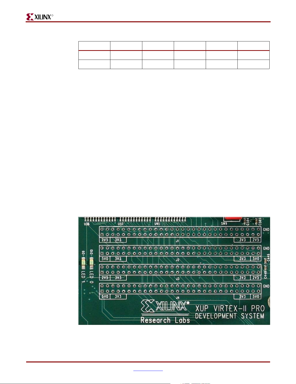
R
Chapter 2: Using the System
Table 2-9: User LED and Switch Connections (Continued)
Signal Direction FPGA Pin I/O Type Drive Slew
PB_LEFT I AH1 LVTTL – –
PB_RIGHT I AH2 LVTTL – –
Using the Expansion Headers and Digilent Expansion Connectors
The XUP Virtex-II Pro Development System allows for four user-supplied expansion
headers that are tailored to accept ribbon cables, and two front mounted connectors that
are designed to accept Digilent peripheral devices and a single Digilent high-speed port. A
total of 80 low-speed signals are provided, with most of the signals shared between the
headers (J1-4) and the front-mounted connectors (J5-6). All of these signals are equipped
with over-voltage protection devices (J34-41) to protect the Virtex-II Pro FPGA. The IDT™
QuickSwitch devices (IDTQS32861) provide protection from signal sources up to 7V.
Tab le 2 -1 0 through Ta bl e 2 -1 6 provide the FPGA connection information and outline the
signals that are shared between the two expansion connector types.
Various power supply voltages are available on the expansion connectors, 2.5V, 3.3V, and
5.0V, depending on the connector type. The expansion headers are positioned to prevent
the installation of a ribbon cable connector across two of the expansion headers. Every
second signal in the ribbon cable is a ground signal to provide the best signal integrity at
the user’s target. The output of the over-voltage protection device follows the input
voltage up to a diode drop below the V
with a V
of 3.3V, the output clamps at -2.5V. This gives 500 mV of input switching
CC
margin for both LVTTL and LVCMOS3.3, which have a V
The expansion headers (J1-J4) are user installed items. These headers can be purchased
from Digikey under the part number S2012-30-ND. Figure 2-14 identifies the location of
the expansion headers.
rail; at which time, the voltage is clamped. So
CC
of 2.0V minimum.
IH
Figure 2-14: Expansion Headers
44 www.xilinx.com XUP Virtex-II Pro Development System
UG069 (v1.0) March 8, 2005
Page 45

Using the Expansion Headers and Digilent Expansion Connectors
In addition to the two low-speed expansion connectors, a single 100-pin high-speed
connector is also provided. This connector provides 40 single-ended user I/Os or 34
differential pairs with additional clock resources. These signals are not shared with any
other connector. Ta bl e 2- 17 provides the pinout information.
The front-mounted Digilent expansion connectors, low speed and high speed, provide the
capability of extending the JTAG-based configuration bitstream to the attached peripheral
cards if required.
For pinout information on the Digilent peripheral boards that are compatible with the XUP
Virtex-II Pro Development System, consult the Digilent Web site at:
http://www.digilentinc.com
Note: In Ta bl e 2 - 10 through Ta bl e 2 - 1 6 , the power rails available on the expansion headers and
connectors are color coded, so they can be easily located in the pinout tables.
Table 2-10: Top Expansion Header Pinout
R
J1
Pin
1
3
5
7
9
Signal
VCC2V5 – – –
VCC2V5 – – –
VCC3V3 – J5.3 J6.3 –
VCC3V3 – J5.3 J6.3 –
VCC3V3 – J5.3 J6.3 –
FPGA
Pin
Digilent
EXP Pin
I/O Type
11 EXP_IO_0 K2 – LVTTL
13 EXP_IO_1 L2 – LVTTL
15 EXP_IO_2 N8 – LVTTL
17 EXP_IO_3 N7 – LVTTL
19 EXP_IO_4 K4 – LVTTL
21 EXP_IO_5 K3 – LVTTL
23 EXP_IO_6 L1 – LVTTL
25 EXP_IO_7 M1 – LVTTL
27 EXP_IO_8 N6 J5.4 LVTTL
29 EXP_IO_9 N5 J5.5 LVTTL
31 EXP_IO_10 L5 J5.6 LVTTL
33 EXP_IO_11 L4 J5.7 LVTTL
35 EXP_IO_12 M2 J5.8 LVTTL
37 EXP_IO_13 N2 J5.9 LVTTL
39 EXP_IO_14 P9 J5.10 LVTTL
41 EXP_IO_15 R9 J5.11 LVTTL
43 EXP_IO_16 M4 J5.12 LVTTL
XUP Virtex-II Pro Development System www.xilinx.com 45
UG069 (v1.0) March 8, 2005
Page 46

R
Chapter 2: Using the System
Table 2-10: Top Expansion Header Pinout (Continued)
J1
Pin
Signal
FPGA
Pin
Digilent
EXP Pin
I/O Type
45 EXP_IO_17 M3 J5.13 LVTTL
47 EXP_IO_18 N1 J5.14 LVTTL
49 EXP_IO_19 P1 J5.15 LVTTL
51
53
55
57
59
VCC3V3 – J5.3 J6.3 –
VCC3V3 – J5.3 J6.3 –
VCC3V3 – J5.3 J6.3 –
VCC2V5 – – –
VCC2V5 – – –
2 GND – J5.1 J6.1 –
4 GND – J5.1 J6.1 –
6 GND – J5.1 J6.1 –
8 GND – J5.1 J6.1 –
10 GND – J5.1 J6.1 –
12 GND – J5.1 J6.1 –
14 GND – J5.1 J6.1 –
16 GND – J5.1 J6.1 –
18 GND – J5.1 J6.1 –
20 GND – J5.1 J6.1 –
22 GND – J5.1 J6.1 –
24 GND – J5.1 J6.1 –
26 GND – J5.1 J6.1 –
28 GND – J5.1 J6.1 –
30 GND – J5.1 J6.1 –
32 GND – J5.1 J6.1 –
34 GND – J5.1 J6.1 –
36 GND – J5.1 J6.1 –
38 GND – J5.1 J6.1 –
40 GND – J5.1 J6.1 –
42 GND – J5.1 J6.1 –
44 GND – J5.1 J6.1 –
46 GND – J5.1 J6.1 –
46 www.xilinx.com XUP Virtex-II Pro Development System
UG069 (v1.0) March 8, 2005
Page 47

Using the Expansion Headers and Digilent Expansion Connectors
Table 2-10: Top Expansion Header Pinout (Continued)
R
J1
Pin
Signal
FPGA
Pin
Digilent
EXP Pin
48 GND – J5.1 J6.1 –
50 GND – J5.1 J6.1 –
52 GND – J5.1 J6.1 –
54 GND – J5.1 J6.1 –
56 GND – J5.1 J6.1 –
58 GND – J5.1 J6.1 –
60 GND – J5.1 J6.1 –
Table 2-11: Upper Middle Expansion Header Pinout
J2|
Pin
1
3
5
Signal
VCC5V0 – J5.2 J6.2 –
VCC5V0 – J5.2 J6.2 –
VCC3V3 – J5.3 J6.3 –
FPGA
Pin
Digilent
EXP Pin
I/O Type
IO Type
7
9
VCC3V3 – J5.3 J6.3 –
VCC3V3 – J5.3 J6.3 –
11 EXP_IO_20 P8 J5.16 LVTTL
13 EXP_IO_21 P7 J5.17 LVTTL
15 EXP_IO_22 N4 J5.18 LVTTL
17 EXP_IO_23 N3 J5.19 LVTTL
19 EXP_IO_24 P3 J5.20 LVTTL
21 EXP_IO_25 P2 J5.21 LVTTL
23 EXP_IO_26 R8 J5.22 LVTTL
25 EXP_IO_27 R7 J5.23 LVTTL
27 EXP_IO_28 P5 J5.24 LVTTL
29 EXP_IO_29 P4 J5.25 LVTTL
31 EXP_IO_30 R2 J5.26 LVTTL
33 EXP_IO_31 T2 J5.27 LVTTL
35 EXP_IO_32 R6 J5.28 LVTTL
37 EXP_IO_33 R5 J5.29 LVTTL
39 EXP_IO_34 R4 J5.30 LVTTL
41 EXP_IO_35 R3 J5.31 LVTTL
XUP Virtex-II Pro Development System www.xilinx.com 47
UG069 (v1.0) March 8, 2005
Page 48
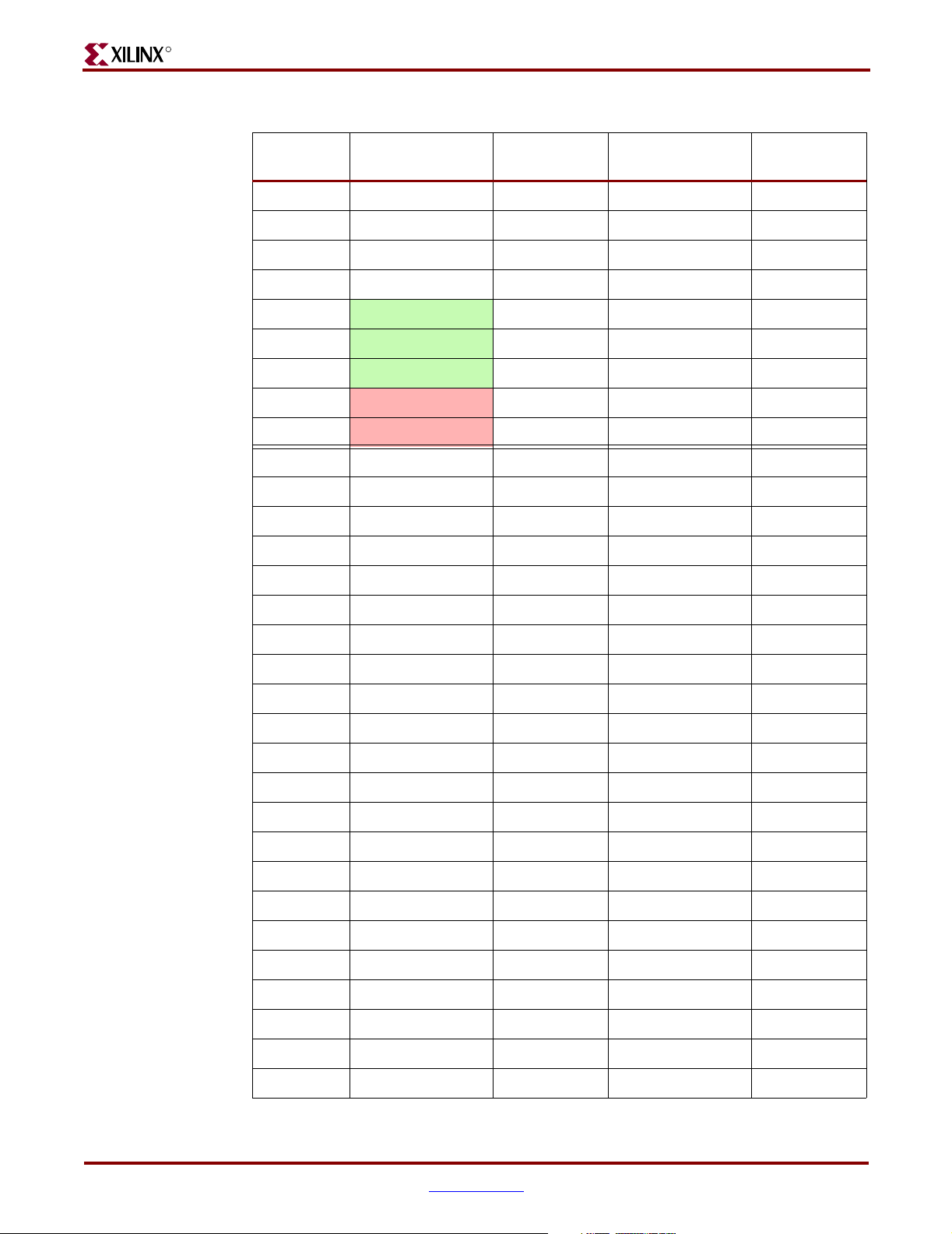
R
Chapter 2: Using the System
Table 2-11: Upper Middle Expansion Header Pinout (Continued)
J2|
Pin
Signal
FPGA
Pin
Digilent
EXP Pin
IO Type
43 EXP_IO_36 U1 J5.32 LVTTL
45 EXP_IO_37 V1 J5.33 LVTTL
47 EXP_IO_38 T5 J5.34 LVTTL
49 EXP_IO_39 T6 J5.35 LVTTL
51
53
55
57
59
VCC3V3 – J5.3 J6.3 –
VCC3V3 – J5.3 J6.3 –
VCC3V3 – J5.3 J6.3 –
VCC5V0 – J5.2 J6.2 –
VCC5V0 – J5.2 J6.2 –
2 GND – J5.1 J6.1 –
4 GND – J5.1 J6.1 –
6 GND – J5.1 J6.1 –
8 GND – J5.1 J6.1 –
10 GND – J5.1 J6.1 –
12 GND – J5.1 J6.1 –
14 GND – J5.1 J6.1 –
16 GND – J5.1 J6.1 –
18 GND – J5.1 J6.1 –
20 GND – J5.1 J6.1 –
22 GND – J5.1 J6.1 –
24 GND – J5.1 J6.1 –
26 GND – J5.1 J6.1 –
28 GND – J5.1 J6.1 –
30 GND – J5.1 J6.1 –
32 GND – J5.1 J6.1 –
34 GND – J5.1 J6.1 –
36 GND – J5.1 J6.1 –
38 GND – J5.1 J6.1 –
40 GND – J5.1 J6.1 –
42 GND – J5.1 J6.1 –
44 GND – J5.1 J6.1 –
48 www.xilinx.com XUP Virtex-II Pro Development System
UG069 (v1.0) March 8, 2005
Page 49

Using the Expansion Headers and Digilent Expansion Connectors
Table 2-11: Upper Middle Expansion Header Pinout (Continued)
R
J2|
Pin
Signal
FPGA
Pin
Digilent
EXP Pin
46 GND – J5.1 J6.1 –
48 GND – J5.1 J6.1 –
50 GND – J5.1 J6.1 –
52 GND – J5.1 J6.1 –
54 GND – J5.1 J6.1 –
56 GND – J5.1 J6.1 –
58 GND – J5.1 J6.1 –
60 GND – J5.1 J6.1 –
Table 2-12: Lower Middle Expansion Header Pinout
J3
Pin
1
3
Signal
VCC2V5 – – –
VCC2V5 – – –
FPGA
Pin
Digilent
EXP Pin
IO Type
IO Type
5
7
9
VCC3V3 – J5.3 J6.3 –
VCC3V3 – J5.3 J6.3 –
VCC3V3 – J5.3 J6.3 –
11 EXP_IO_40 T3 J5.36 LVTTL
13 EXP_IO_41 T4 J5.37 LVTTL
15 EXP_IO_42 U2 J5.38 LVTTL
17 EXP_IO_43 U3 J5.39 LVTTL
19 EXP_IO_44 T7 J5.40 LVTTL
21 EXP_IO_45 T8 J6.5 LVTTL
23 EXP_IO_46 U4 J6.4 LVTTL
25 EXP_IO_47 U5 J6.7 LVTTL
27 EXP_IO_48 V2 J6.6 LVTTL
29 EXP_IO_49 W2 J6.9 LVTTL
31 EXP_IO_50 T9 J6.8 LVTTL
33 EXP_IO_51 U9 J6.11 LVTTL
35 EXP_IO_52 V3 J6.10 LVTTL
37 EXP_IO_53 V4 J6.13 LVTTL
39 EXP_IO_54 W1 J6.12 LVTTL
XUP Virtex-II Pro Development System www.xilinx.com 49
UG069 (v1.0) March 8, 2005
Page 50
R
Chapter 2: Using the System
Table 2-12: Lower Middle Expansion Header Pinout (Continued)
J3
Pin
Signal
FPGA
Pin
Digilent
EXP Pin
IO Type
41 EXP_IO_55 Y1 J6.15 LVTTL
43 EXP_IO_56 U7 J6.14 LVTTL
45 EXP_IO_57 U8 J6.17 LVTTL
47 EXP_IO_58 V5 J6.16 LVTTL
49 EXP_IO_59 V6 J6.19 LVTTL
51
53
55
57
59
VCC3V3 – J5.3 J6.3 –
VCC3V3 – J5.3 J6.3 –
VCC3V3 – J5.3 J6.3 –
VCC2V5 – – –
VCC2V5 – – –
2 GND – J5.1 J6.1 –
4 GND – J5.1 J6.1 –
6 GND – J5.1 J6.1 –
8 GND – J5.1 J6.1 –
10 GND – J5.1 J6.1 –
12 GND – J5.1 J6.1 –
14 GND – J5.1 J6.1 –
16 GND – J5.1 J6.1 –
18 GND – J5.1 J6.1 –
20 GND – J5.1 J6.1 –
22 GND – J5.1 J6.1 –
24 GND – J5.1 J6.1 –
26 GND – J5.1 J6.1 –
28 GND – J5.1 J6.1 –
30 GND – J5.1 J6.1 –
32 GND – J5.1 J6.1 –
34 GND – J5.1 J6.1 –
36 GND – J5.1 J6.1 –
38 GND – J5.1 J6.1 –
40 GND – J5.1 J6.1 –
42 GND – J5.1 J6.1 –
50 www.xilinx.com XUP Virtex-II Pro Development System
UG069 (v1.0) March 8, 2005
Page 51
Using the Expansion Headers and Digilent Expansion Connectors
Table 2-12: Lower Middle Expansion Header Pinout (Continued)
R
J3
Pin
Signal
FPGA
Pin
Digilent
EXP Pin
44 GND – J5.1 J6.1 –
46 GND – J5.1 J6.1 –
48 GND – J5.1 J6.1 –
50 GND – J5.1 J6.1 –
52 GND – J5.1 J6.1 –
54 GND – J5.1 J6.1 –
56 GND – J5.1 J6.1 –
58 GND – J5.1 J6.1 –
60 GND – J5.1 J6.1 –
Table 2-13: Bottom Expansion Header Pinout
J4
Pin
1
Signal
VCC5V0 – J5.2 J6.2 –
FPGA
Pin
Digilent
EXP Pin
IO Type
IO Type
3
5
7
9
VCC5V0 – J5.2 J6.2 –
VCC3V3 – J5.3 J6.3 –
VCC3V3 – J5.3 J6.3 –
VCC3V3 – J5.3 J6.3 –
11 EXP_IO_60 Y2 J6.18 LVTTL
13 EXP_IO_61 AA2 J6.21 LVTTL
15 EXP_IO_62 V7 J6.20 LVTTL
17 EXP_IO_63 V8 J6.23 LVTTL
19 EXP_IO_64 W3 J6.22 LVTTL
21 EXP_IO_65 W4 J6.25 LVTTL
23 EXP_IO_66 AA1 J6.24 LVTTL
25 EXP_IO_67 AB1 J6.27 LVTTL
27 EXP_IO_68 W5 J6.26 LVTTL
29 EXP_IO_69 W6 J6.29 LVTTL
31 EXP_IO_70 Y4 J6.28 LVTTL
33 EXP_IO_71 Y5 J6.31 LVTTL
35 EXP_IO_72 AA3 J6.30 LVTTL
37 EXP_IO_73 AA4 J6.33 LVTTL
XUP Virtex-II Pro Development System www.xilinx.com 51
UG069 (v1.0) March 8, 2005
Page 52

R
Chapter 2: Using the System
Table 2-13: Bottom Expansion Header Pinout (Continued)
J4
Pin
Signal
FPGA
Pin
Digilent
EXP Pin
IO Type
39 EXP_IO_74 W7 J6.32 LVTTL
41 EXP_IO_75 W8 J6.35 LVTTL
43 EXP_IO_76 AB3 J6.34 –v
45 EXP_IO_77 AB4 – –
47 EXP_IO_78 AB2 – –
49 EXP_IO_79 AC2 – –
51
53
55
57
59
VCC3V3 – J5.3 J6.3 –
VCC3V3 – J5.3 J6.3 –
VCC3V3 – J5.3 J6.3 –
VCC5V0 – J5.2 J6.2 –
VCC5V0 – J5.2 J6.2 –
2 GND – J5.1 J6.1 –
4 GND – J5.1 J6.1 –
6 GND – J5.1 J6.1 –
8 GND – J5.1 J6.1 –
10 GND – J5.1 J6.1 –
12 GND – J5.1 J6.1 –
14 GND – J5.1 J6.1 –
16 GND – J5.1 J6.1 –
18 GND – J5.1 J6.1 –
20 GND – J5.1 J6.1 –
22 GND – J5.1 J6.1 –
24 GND – J5.1 J6.1 –
26 GND – J5.1 J6.1 –
28 GND – J5.1 J6.1 –
30 GND – J5.1 J6.1 –
32 GND – J5.1 J6.1 –
34 GND – J5.1 J6.1 –
36 GND – J5.1 J6.1 –
38 GND – J5.1 J6.1 –
40 GND – J5.1 J6.1 –
52 www.xilinx.com XUP Virtex-II Pro Development System
UG069 (v1.0) March 8, 2005
Page 53

Using the Expansion Headers and Digilent Expansion Connectors
Table 2-13: Bottom Expansion Header Pinout (Continued)
R
J4
Pin
Signal
FPGA
Pin
Digilent
EXP Pin
42 GND – J5.1 J6.1 –
44 GND – J5.1 J6.1 –
46 GND – J5.1 J6.1 –
48 GND – J5.1 J6.1 –
50 GND – J5.1 J6.1 –
52 GND – J5.1 J6.1 –
54 GND – J5.1 J6.1 –
56 GND – J5.1 J6.1 –
58 GND – J5.1 J6.1 –
60 GND – J5.1 J6.1 –
Table 2-14: Left Digilent Expansion Connector Pinout
J5
PIN
Signal
FPGA
Pin
Expansion
Header Pin
IO Type
IO Type
1 GND – J1-4 EVEN PINS –
3
VCC3V3 – – –
5 EXP_IO_9 N5 J1.29 LVTTL
7 EXP_IO_11 L4 J1.33 LVTTL
9 EXP_IO_13 N2 J1.37 LVTTL
11 EXP_IO_15 R9 J1.41 LVTTL
13 EXP_IO_17 M3 J1.45 LVTTL
15 EXP_IO_19 P1 J1.49 LVTTL
17 EXP_IO_21 P7 J2.13 LVTTL
19 EXP_IO_23 N3 J2.17 LVTTL
21 EXP_IO_25 P2 J2.21 LVTTL
23 EXP_IO_27 R7 J2.25 LVTTL
25 EXP_IO_29 P4 J2.29 LVTTL
27 EXP_IO_31 T2 J2.33 LVTTL
29 EXP_IO_33 R5 J2.37 LVTTL
31 EXP_IO_35 R3 J2.41 LVTTL
33 EXP_IO_37 V1 J2.45 LVTTL
35 EXP_IO_39 T6 J2.49 LVTTL
XUP Virtex-II Pro Development System www.xilinx.com 53
UG069 (v1.0) March 8, 2005
Page 54
R
Chapter 2: Using the System
Table 2-14: Left Digilent Expansion Connector Pinout (Continued)
J5
PIN
Signal
FPGA
Pin
Expansion
Header Pin
IO Type
31 EXP_IO_35 R3 J2.41 LVTTL
33 EXP_IO_37 V1 J2.45 LVTTL
35 EXP_IO_39 T6 J2.49 LVTTL
37 EXP_IO_41 T4 J3.13 LVTTL
39 EXP_IO_43 U3 J3.17 LVTTL
2
VCC5VO – –
4 EXP_IO_8 N6 J1.27 LVTTL
6 EXP_IO_10 L5 J1.31 LVTTL
8 EXP_IO_12 M2 J1.35 LVTTL
10 EXP_IO_14 P9 J1.39 LVTTL
12 EXP_IO_16 M4 J1.43 LVTTL
14 EXP_IO_18 N1 J1.47 LVTTL
16 EXP_IO_20 P8 J2.11 LVTTL
18 EXP_IO_22 N4 J2.15 LVTTL
20 EXP_IO_24 P3 J2.19 LVTTL
22 EXP_IO_26 R8 J2.23 LVTTL
24 EXP_IO_28 P5 J2.27 LVTTL
26 EXP_IO_30 R2 J2.31 LVTTL
28 EXP_IO_32 R6 J2.35 LVTTL
30 EXP_IO_34 R4 J2.39 LVTTL
32 EXP_IO_36 U1 J2.43 LVTTL
34 EXP_IO_38 T5 J2.47 LVTTL
36 EXP_IO_40 T3 J3.11 LVTTL
38 EXP_IO_42 U2 J3.13 LVTTL
40 EXP_IO_44 U7 J3.19 LVTTL
Table 2-15: Right Digilent Expansion Connector Pinout
J5
PIN
Signal
FPGA
Pin
Expansion
Header Pin
1 GND – J1-4 EVEN PINS –
IO Type
3
VCC3V3 – – –
5 EXP_IO_45 T8 J3.21 LVTTL
54 www.xilinx.com XUP Virtex-II Pro Development System
UG069 (v1.0) March 8, 2005
Page 55
Using the Expansion Headers and Digilent Expansion Connectors
Table 2-15: Right Digilent Expansion Connector Pinout (Continued)
R
J5
PIN
Signal
FPGA
Pin
Expansion
Header Pin
IO Type
7 EXP_IO_47 U5 J3.25 LVTTL
9 EXP_IO_49 W2 J3.29 LVTTL
11 EXP_IO_51 U9 J3.33 LVTTL
13 EXP_IO_53 V4 J3.37 LVTTL
15 EXP_IO_55 Y1 J3.41 LVTTL
17 EXP_IO_57 U8 J3.45 LVTTL
19 EXP_IO_59 V6 J3.49 LVTTL
21 EXP_IO_61 AA2 J4.13 LVTTL
23 EXP_IO_63 V8 J4.17 LVTTL
25 EXP_IO_65 W4 J4.21 LVTTL
27 EXP_IO_67 AB1 J4.25 LVTTL
29 EXP_IO_69 W6 J4.29 LVTTL
31 EXP_IO_71 Y5 J4.33 LVTTL
33 EXP_IO_73 AA4 J4.37 LVTTL
35 EXP_IO_75 W8 J4.41 LVTTL
37 FPGA_TMS H8 – LVTTL
39 LS_EXP_TDO – – LVTTL
2
VCC5V0 – – –
4 EXP_IO_46 U4 J3.23 LVTTL
6 EXP_IO_48 V2 J3.27 LVTTL
8 EXP_IO_50 T9 J3.31 LVTTL
10 EXP_IO_52 V3 J3.35 LVTTL
12 EXP_IO_54 W1 J3.39 LVTTL
14 EXP_IO_56 U7 J3.43 LVTTL
16 EXP_IO_58 V5 J3.47 LVTTL
18 EXP_IO_60 Y2 J4.11 LVTTL
20 EXP_IO_62 V7 J4.15 LVTTL
22 EXP_IO_64 W3 J4.19 LVTTL
24 EXP_IO_66 AA1 J4.23 LVTTL
26 EXP_IO_68 W5 J4.27 LVTTL
28 EXP_IO_70 Y4 J4.31 LVTTL
XUP Virtex-II Pro Development System www.xilinx.com 55
UG069 (v1.0) March 8, 2005
Page 56

R
Chapter 2: Using the System
Table 2-15: Right Digilent Expansion Connector Pinout (Continued)
J5
PIN
Signal
FPGA
Pin
Expansion
Header Pin
30 EXP_IO_72 AA3 J4.35 LVTTL
32 EXP_IO_74 W7 J4.39 LVTTL
34 EXP_IO_74 AB3 J4.43 LVTTL
36 JTAG_EXP_SEL – – LVTTL
38 FPGA_TCK G7 – LVTTL
40 FPGA_TDO F5 – LVTTL
Table 2-16: High-Speed Digilent Expansion Connector Pinout
J37
PIN
A01
A02
Signal
VCC3V3 – – –
VCC3V3 – – –
FPGA
Pin
Differential
Pair
A03 FPGA_TMS – – –
A04 HS_JTAG_EXP_SEL – – –
IO Type
I/O Type
A05 HS_EXP_TDO – – –
A06 HS_IO_1 AF6 31P_3 LVTTL
A07 HS_IO_2 AE5 31N_3 LVTTL
A08 HS_IO_3 AB8 32P_3 LVTTL
A09 HS_IO_4 AB7 32N_3 LVTTL
A10 HS_IO_5 AE4 33P_3 LVTTL
A11 HS_IO_6 AE3 33N_3 LVTTL
A12 HS_IO_7 AF4 34P_3 LVTTL
A13 HS_IO_8 AF3 34N_3 LVTTL
A14 HS_IO_9 AC6 35P_3 LVTTL
A15 HS_IO_10 AC5 35N_3 LVTTL
A16 HS_IO_11 AF2 36P_3 LVTTL
A17 HS_IO_12 AF1 36N_3 LVTTL
A18 HS_IO_13 AD4 37P_3 LVTTL
A19 HS_IO_14 AD3 37N_3 LVTTL
A20 HS_IO_15 AA8 38P_3 LVTTL
A21 HS_IO_16 AA7 38N_3 LVTTL
A22 HS_IO_17 AE2 39P_3 LVTTL
56 www.xilinx.com XUP Virtex-II Pro Development System
UG069 (v1.0) March 8, 2005
Page 57

Using the Expansion Headers and Digilent Expansion Connectors
Table 2-16: High-Speed Digilent Expansion Connector Pinout (Continued)
R
J37
PIN
Signal
FPGA
Pin
Differential
Pair
I/O Type
A23 HS_IO_18 AE1 39N_3 LVTTL
A24 HS_IO_19 AB6 40P_3 LVTTL
A25 HS_IO_20 AB5 40N_3 LVTTL
A26 HS_IO_21 Y8 41P_3 LVTTL
A27 HS_IO_22 Y7 41N_3 LVTTL
A28 HS_IO_23 AD2 42P_3 LVTTL
A29 HS_IO_24 AD1 42N_3 LVTTL
A30 HS_IO_25 L7 41P_2 LVTTL
A31 HS_IO_26 L8 41N_2 LVTTL
A32 HS_IO_27 G1 40P_2 LVTTL
A33 HS_IO_28 G2 40N_2 LVTTL
A34 HS_IO_29 G3 39P_2 LVTTL
A35 HS_IO_30 G4 39N_2 LVTTL
A36 HS_IO_31 J5 38P_2 LVTTL
A37 HS_IO_32 J6 38P_2 LVTTL
A38 HS_IO_33 F1 37P_2 LVTTL
A39 HS_IO_34 F2 37P_2 LVTTL
A40 HS_IO_35 F3 36P_2 LVTTL
A41 HS_IO_36 F4 36N_2 LVTTL
A42 HS_IO_37 K7 35P_2 LVTTL
A43 HS_IO_38 K8 35N_2 LVTTL
A44 HS_IO_39 E1 34P_2 LVTTL
A45 HS_IO_40 E2 34N_2 LVTTL
A46 GND – – –
A47 HS_CLKOUT E4 33N_2 LVTTL
A48 GND – – –
A49
A50
VCC5V0 – – –
VCC5V0 – – –
B01 SHIELD – – –
B02 GND – – –
B03 LS_EXP_FPGA_TDO – – –
XUP Virtex-II Pro Development System www.xilinx.com 57
UG069 (v1.0) March 8, 2005
Page 58

R
Chapter 2: Using the System
Table 2-16: High-Speed Digilent Expansion Connector Pinout (Continued)
J37
PIN
Signal
B04 FPGA_TCK – – –
B05-B45 GND – – –
B46 HS_CLKIN B16 (GCLK6S) No_Pair LVCMOS25
B47 GND – – –
B48 HS_CLKIO E3 33P_2 LVTTL
B49
VCC5V5 – – –
B50 SHIELD – – –
Using the CPU Debug Port and CPU Reset
The CPU Debug port (J36) is a right angle header that provides connections to the
debugging resources of the PowerPC 405 CPU core.
The PowerPC 405 CPU cores include dedicated debug resources that support a variety of
debug modes for debugging during hardware and software development. These debug
resources include:
• Internal debug mode for use by ROM monitors and software debuggers
• External debug mode for use by JTAG debuggers
• Debug wait mode, which allows the servicing of interrupts while the processor
appears to be stopped
• Real-time trace mode, which supports event triggering for real time tracing
FPGA
Pin
Differential
Pair
I/O Type
Debug modes and events are controlled using debug registers in the processor. The debug
registers are accessed either through software running on the processor or through the
JTAG port. The debug modes, events, controls, and interfaces provide a powerful
combination of debug resources for hardware and software development tools.
The JTAG port interface supports the attachment of external debug tools, such as the
powerful ChipScope™ Integrated Logic Analyzer, a powerful tool providing logic
analyzer capabilities for signals inside an FPGA, without the need for expensive external
instrumentation. Using the JTAG test access port, a debug tool can single-step the
processor and examine the internal processor state to facilitate software debugging. This
capability complies with standard JTAG hardware for boundary scan system testing.
External debug mode can be used to alter normal program execution. It provides the
ability to debug system hardware as well as software. The mode supports multiple
functions: starting and stopping the processor, single-stepping instruction execution,
setting breakpoints, as well as monitoring processor status. Access to processor resources
is provided through the CPU Debug Port.
The PPC405 JTAG Debug Port supports the four required JTAG signals: CPU_TCK,
CPU_TMS, CPU_TDO, and CPU_TDI. It also implements the optional CPU_TRST signal.
The frequency of the JTAG clock signal, CPU_TCK, can range from 0 MHz up to one-half
of the processor clock frequency. The JTAG debug port logic is reset at the same time the
system is reset, using the CPU_TRST signal. When CPU_TRST is asserted, the JTAG TAP
controller returns to the test-logic reset state.
58 www.xilinx.com XUP Virtex-II Pro Development System
UG069 (v1.0) March 8, 2005
Page 59
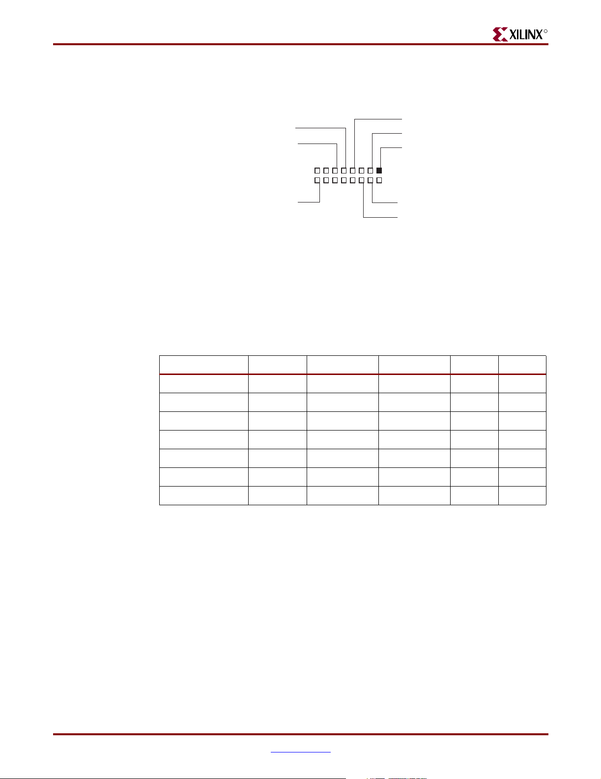
Using the CPU Debug Port and CPU Reset
Figure 2-15 shows the pinout of the header used to debug the operation of software in the
CPU. This is accomplished using debug tools, such as the Xilinx Parallel Cable IV or third
party tools.
R
CPU TMS
CPU HALT Z
15 1
16
GND
CPU TCK
CPU TDI
CPU TDO
2
CPU TRST
3.3V
UG069_15_082404
Figure 2-15: CPU Debug Connector Pinouts
The JTAG debug resources are not hardwired to specific pins and are available for
attachment in the FPGA fabric, making it possible to route these signals to whichever
FPGA pins the user prefers to use. The signal-pin connections used on the XUP VirtexII Pro Development System are identified in Tab le 2- 17 along with the recommended I/O
characteristics. Level shifting circuitry is provided for all signals to convert from the 3.3V
levels at the connector to the 2.5V levels at the FPGA.
Table 2-17: CPU Debug Port Connections and CPU Reset
Signal Direction FPGA Pin I/O Type DRIVE Slew
PROC_RESET_Z I AH5 LVTTL – –
CPU_TDO O AG16 LVCMOS25 12 mA SLOW
CPU_TDI I AF15 LVCMOS25 – –
CPU_TMS I AJ16 LVCMOS25 – –
CPU_TCK I AG15 LVCMOS25 – –
CPU_TRST I AC21 LVCMOS25 – –
CPU_HALT_Z I AJ23 LVCMOS25 – –
The RESET_RELOAD pushbutton (SW1) provides two different functions depending on
how long the switch is depressed. If the switch is activated for more than 2 seconds, the
XUP Virtex-II Pro Development System undergoes a complete reset and reloads the
selected configuration. If, however, the switch is activated for less than 2 seconds, a
XUP Virtex-II Pro Development System www.xilinx.com 59
UG069 (v1.0) March 8, 2005
Page 60

R
Chapter 2: Using the System
processor reset pulse of 100 microseconds is applied to the PROCESSOR_RESET_Z signal.
The RESET_RELOAD circuit is shown in Figure 2-16.
ug069_16_021505
Figure 2-16: RELOAD and CPU RESET Circuit
Using the Serial Ports
Serial ports are useful as simple, low-speed interfaces. These ports can provide
communication between a Host machine and a Peripheral machine, or Host-to-Host
communications. The XUP Virtex-II Pro Development System provides two different types
of serial ports, a single RS-232 port and two PS/2 ports.
The RS-232 standard specifies output voltage levels between -5V to -15V for a logical 1, and
+5V to +15V for a logical 0. Inputs must be compatible with voltages in the range -3V to 15V for a logical 1 and +3V to +15V for a logical 0. This ensures that data is correctly read
even at the maximum cable length of 50 feet. These signaling levels are outside the range of
voltages that can be supported by the Virtex-II Pro family of FPGAs, requiring the use of a
transceiver. The connector is a DCE-style that allows the use of a straight-through 9-pin
serial cable to connect to the DTE-style serial port connector available on most personal
computers and workstations. A null-modem cable is not required. Figure 2-17 shows the
implementation of the serial port used on the XUP Virtex-II Pro Development System.
The MAX3388E is a 2.5V powered device that operates as a transceiver to shift the
signaling levels from the voltages supported by the FPGA to those required by the RS-232
specification. The MAX3388E has two receivers and three transmitters and is capable of
running at data rates up to 460 kb/s while maintaining RS-232-compliant output levels.
There are five signals from the FPGA to the RS-232 serial port: RS232_TX_DATA,
RS232_DSR_OUT, RS232_CTS_OUT, RS232_RX_DATA, and RS232_RTS_IN. The Transmit
Data and Receive Data provide bidirectional data transmission, while Request To Send,
Clear To Send, and Data Set Ready provide for hardware flow control across the serial link.
Tab le 2 -1 7 identifies the RS-232 signal connections to the FPGA.
IBM developed the PS/2 ports for peripherals as an alternative to serial ports and
dedicated keyboard ports. These ports have become standard connectors on PCs for
connecting both keyboards and mice. They use a 6-pin mini-DIN connector and a
bidirectional synchronous serial interface, with a bidirectional data signal and a
unidirectional clock. The XUP Virtex-II Pro Development System provides two PS/2 ports,
for keyboard and mouse attachment. The PC mouse and keyboard use the two-wire RS/2
serial bus to communicate with the host FPGA. The PS/2 bus includes both clock and data
with identical signal timings and both user 11-bit data words that include a start bit, stop
60 www.xilinx.com XUP Virtex-II Pro Development System
UG069 (v1.0) March 8, 2005
Page 61

Using the Serial Ports
R
bit, and odd parity. The data packets are organized differently for mouse and keyboard
data. In addition, the keyboard interface supports bidirectional data transfer so the host
device can drive the status LEDs on the keyboard.
VCC2V5
RS232_DSR_OUT
RS232_TX_DATA
RS232_CTS_OUT
RS232_RX_DATA
RS232_RTS_IN
0.1UF
0.1UF
C446
C449
1
3
4
5
7
8
9
13
12
10
11
24 23 14
SHDN
VCC VL
C1+
2.5V RS-232
C1-
Transceiver
C2+
C1-
T1IN
T2IN
T3IN
R1OUT
R2OUT
LOUT
SWOUT
GND
T1OUT
T2OUT
T3OUT
R1IN
R2IN
SWIN
22
2
V+
6
V-
21
20
19
18
17
16
LIN
15
MAC3388ECUG
C447
0.1UF
C448
0.1UF
DSR
RXD
CTS
TXD
RTS
C445U28
0.1UF
J11
1
2
3
4
5
6
7
8
9
RS-232 DCE
UG069_17_021405
Figure 2-17: RS-232 Serial Port Implementation
The PS/2 port operates as a serial interface with a bidirectional data signal and a
unidirectional clock signal. Both of these signals operate as open-drain signals, defaulting
to a logical 1, at 5V through the use of a week pull-up resistor. To transmit a logical 0, the
signal line is actively pulled to ground. In the case of the data line, both the host and the
attached peripheral are able to drive the signal low. In the case of the clock signal, only the
host is able to drive the signal low, giving the host control of the speed of the interface.
Figure 2-18 shows the implementation of the PS/2 keyboard port used on the XUP Virtex-
II Pro Development System. The implementation of the PS/2 mouse port is identical
except for the signal names and the part reference designator.
The bidirectional level shifter shown in Figure 2-18 is used to interconnect two sections of
the PS/2 port, each section with a different power supply voltage and different logic levels.
The level shifter for each signal consists of one discrete N-channel enhancement MOS-FET.
The gate of the transistor must be connected to the lowest supply voltage (VCC3V3); the
source connects to the signal on the lower voltage side; and the drain connects to the signal
on the higher voltage side.
XUP Virtex-II Pro Development System www.xilinx.com 61
UG069 (v1.0) March 8, 2005
Page 62

R
VCC5V0
Chapter 2: Using the System
.
VCC3V3
R106
2K0
KBD_CLOCK
KBD_DATA
UG069_18_101804
J12A
UPPER
STACKED_PS2_6PIN
L54
HZ0805E601R-00
L53 HZ0805E601R-00
C441
470PF
BIDIRECTIONAL
LEVEL
SHIFTER
R108
R107
3K3
3K3
C442
470PF
GNDGNDGND
3
3
U24
BSS138
D
U25
U24
BSS138
BSS138
D
3
0
3
0
H CHAH H CHAH
2
1
2
1
R105
2K0
Figure 2-18: PS/2 Serial Port Implementation
If no device is actively pulling the signal low, the pull-up resistor pulls up the signal on the
FPGA side. The gate and source of the MOS-FET are both at the same potential and the
MOS-FET is not conducting. This allows the signal on the peripheral side to be pulled up
by the pull-up resistor. So both sections of the signal are high, but at different voltage
levels.
If the FPGA actively pulls the signal low, the MOS-FET begins to conduct and pulls the
peripheral side low as well.
If the peripheral side pulls the signal low, the FPGA side is initially pulled low via the
drain-substrate diode of the MOS-FET. After the threshold is passed, the MOS-FET begins
to conduct and the signal is further pulled down via the conducting MOS-FET.
Tab le 2 -1 8 identifies the PS/2 signal connections to the FPGA.
Table 2-18: Keyboard, Mouse, and RS-232 Connections
Signal Direction FPGA Pin I/O Type Drive Slew
KBD_CLOCK I/O AG2 LVTTL 8 mA SLOW
KBD_DATA I/O AG1 LVTTL 8 mA SLOW
MOUSE_CLOCK I/O AD6 LVTTL 8 mA SLOW
MOUSE_DATA I/O AD5 LVTTL 8 mA SLOW
RS232_TX_DATA O AE7 LVCMOS25 8 mA SLOW
RS232_RX_DATA I AJ8 LVCMOS25 – –
RS232_DSR_OUT O AD10 LVCMOS25 8 mA SLOW
RS232_CTS_OUT O AE8 LVCMOS25 8 mA SLOW
RS232_RTS_IN I AK8 LVCMOS25 – –
Using the Fast Ethernet Network Interface
The 10/100 Ethernet is a network protocol, defined by the IEEE 802.3 standard, which
includes a 10 Mb/s Ethernet and a 100 Mb/s Ethernet. The XUP Virtex-II Pro
Development System has been designed to support Internet connectivity using an
Ethernet connection.
62 www.xilinx.com XUP Virtex-II Pro Development System
UG069 (v1.0) March 8, 2005
Page 63

Using the Fast Ethernet Network Interface
The Ethernet network interface is made up of three distinct components: the Media Access
Controller (MAC) contained in the FPGA, a physical layer transceiver (PHY), and the
Ethernet coupling magnetics.
The LXT972A (U12) is an IEEE 802.3-compliant Fast Ethernet physical layer (PHY)
transceiver that supports both 100BASE-TX and 10BASE-T operation. It provides the
standard Media Independent Interface (MII) for easy attachment to 10/100 (MACs). The
LXT972A supports full-duplex operation at 10 Mb/s and 100 Mb/s. The operational mode
can be set using auto-negotiation, parallel detection, or manual control.
The LXT972A performs all functions of the physical coding sublayer (PCS), the physical
media attachment (PMA) sublayer, and the physical media dependent (PMD) sublayer for
100BASE-TX connections.
The LXT972A reads its three configuration pins on power up to check for forced operation
settings. If it is not configured for forced operation at 10 Mb/s or 100 Mb/s, the device uses
auto-negotiation/parallel detection to automatically determine line operating conditions.
If the PHY on the other end of the link supports auto-negotiation, the LXT972A autonegotiates with it, using fast link pulse (FLP) bursts. If the other PHY does not support
auto-negotiation, the LXT972A automatically detects the presence of either link pulses
(10BASE-T) or idle symbols (100BASE-TX) and sets its operating mode accordingly.
The LXT972A configuration pins are set to allow for auto-negotiation, 10 Mb/s or
100 Mb/s, full-duplex or half-duplex operation. These settings can be overridden by
setting control bits in the Media Independent Interface (MII) registers.
R
The slew rate of the transmitter outputs is controlled by the two slew control inputs. It is
recommended that the slowest slew rate be set by driving both of the slew inputs with a
logical 1.
Three LEDs are available to provide visual status information about the Ethernet link
connection. If a link has been established, the LINK UP LED is turned on. If the link is a
100 Mb/s link, then the SPEED LED also turns on. The RX_DATA LED blinks, indicating
that packets are being received. Setting control bits in the MII registers can alter the
function of the three LEDs.
The LX972A provides the interface to the physical media; the MAC resides in the FPGA
and is available as an IP core.
The 10/100 Ethernet requires transformer coupling between the PHY and the RJ-45
connector to provide electrical protection to the system. The magnetics used on the XUP
Virtex-II Pro Development System are integrated into the RJ45 connector (J10) from the
FastJack™ series of connectors from Halo Electronics, Inc. The HFJ11-2450 provides a
significant real estate reduction over non-integrated solutions. Tab le 2- 18 identifies the
connections between the FPGA and the PHY.
The type of network cable that is used with the XUP Virtex-II Pro Development System
depends on how the system is connected to the network. If the XUP Virtex-II Pro
Development System is connected directly to a host computer, then a cross-over Ethernet
cable is required. However, if the system is connected to the network through a hub or
router, then a normal straight-through Ethernet cable is required.
XUP Virtex-II Pro Development System www.xilinx.com 63
UG069 (v1.0) March 8, 2005
Page 64
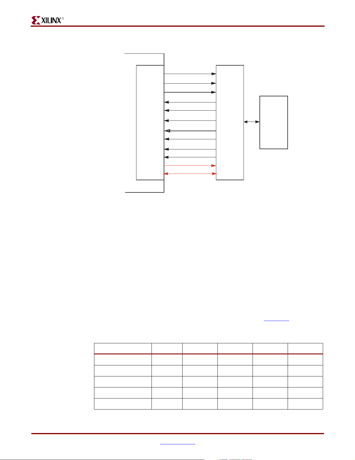
R
Chapter 2: Using the System
Figure 2-19 provides a block diagram of the Ethernet interface.
FPGA
MAC IP
TX_ERROR
TX_ENABLE
TX_DATA[3:0]
TX_CLOCK
RX_CLOCK
RX_DATA[3:0]
RX_ERROR
RX_DATA_VALID
CARRIER_SENSE
COLLISION
MDC
MDIO
LXT972A
Magnetics
RJ-45
UG069_19_012505
Figure 2-19: 10/100 Ethernet Interface Block Diagram
The XUP Virtex-II Pro Development System includes a Dallas Semiconductor DS2401P
Silicon Serial Number (U13). This device provides a unique identity for each circuit board
which can be determined with a minimal electronic interface. The DS2401P consists of a
factory laser programmed, 64-bit ROM that includes a unique 48-bit serial number, an 8-bit
CRC, and an 8-bit family device code. Data is transferred serially via the 1-Wire protocol,
which requires only a single data lead and a ground return. Power for reading the device
is derived from the data line with no requirement for an additional power supply. The
unique 48-bit serial number should not be used as the MAC address for the Ethernet
interface, because this number has not been registered as a valid Ethernet MAC address.
The XUP Virtex-II Pro Development System printed circuit board includes a label that
contains the board serial number, obtained from the DS2401P Silicon Serial Number, as
well as a valid Ethernet MAC address that has been registered with the IEEE. Xilinx
maintains a cross reference list matching the board serial number with the assigned
Ethernet MAC address on the XUP Virtex-II Pro Development System support Web page.
Xilinx provides the IP for the 1-Wire interface and application note XAPP198
Synthesizable
FPGA Interface for Retrieving ROM Number from 1-Wire Devices describes this interface.
Table 2-19: 10/100 ETHERNET Connections
Signal Direction FPGA Pin I/O Type Drive Slew
TX_DATA[0] O J7 LVTTL 8 mA SLOW
TX_DATA[1] O J8 LVTTL 8 mA SLOW
TX_DATA[2] O C1 LVTTL 8 mA SLOW
TX_DATA[3] O C2 LVTTL 8 mA SLOW
TX_ERROR O H2 LVTTL 8 mA SLOW
64 www.xilinx.com XUP Virtex-II Pro Development System
UG069 (v1.0) March 8, 2005
Page 65

Using System ACE Controllers for Non-Volatile Storage
Table 2-19: 10/100 ETHERNET Connections (Continued)
Signal Direction FPGA Pin I/O Type Drive Slew
TX_CLOCK I D3 LVTTL – –
TX_ENABLE O C4 LVTTL 8 mA SLOW
RX_DATA[0] I K6 LVTTL – –
RX_DATA[1] I K5 LVTTL – –
RX_DATA[2] I J1 LVTTL – –
RX_DATA[3] I K1 LVTTL – –
RX_DATA_VALID I M7 LVTTL – –
RX_ERROR I J2 LVTTL – –
RX_CLOCK I M8 LVTTL – –
ENET_RESET_Z O G6 LVTTL 8 mA SLOW
CARRIER_SENSE I C5 LVTTL – –
R
COL_DETECT I D5 LVTTL – –
ENET_SLEW0 O B3 LVTTL 8 mA SLOW
ENET_SLEW1 O A3 LVTTL 8 mA SLOW
MDIO I/O M5 LVTTL 8 mA SLOW
MDC O M6 LVTTL 8 mA SLOW
MDINIT_Z I G5 LVTTL – –
PAUSE O J4 LVTTL 8 mA SLOW
SSN_DATA I J3 LVTTL 8 mA SLOW
Using System ACE Controllers for Non-Volatile Storage
In addition to programming the FPGA and storing bitstreams, the System ACE controller
can be used for general-purpose non-volatile storage. Each System ACE controller
provides an MPU interface to allow a microprocessor to access the attached CompactFlash
or IBM Microdrive, allowing this storage media to be used as a file system.
The MPU interface provides a useful means of monitoring the status of and controlling the
System ACE controller, as well as CompactFlash card READ/WRITE data. The MPU is not
required for normal operation, but when it is used, it provides numerous capabilities. This
interface enables communication between an MPU device, a CompactFlash card, and the
FPGA target system.
The MPU interface is composed of a set of registers that provide a means for
communicating with CompactFlash control logic, configuration control logic, and other
resources in the System ACE controller. This interface can be used to read the identity of a
CompactFlash device and read/write sectors from or to a CompactFlash device.
The MPU interface can also be used to control configuration flow. It enables monitoring of
the configuration status and error conditions. The MPU interface can be used to delay
XUP Virtex-II Pro Development System www.xilinx.com 65
UG069 (v1.0) March 8, 2005
Page 66
R
Chapter 2: Using the System
configuration, start configuration, select the source of configuration, control the bitstream
revision, and reset the device.
For the System ACE controller to be properly synchronized with the MPU, the clocks must
be synchronized. The clock traces on the XUP Virtex-II Pro Development System that drive
the System ACE controller and the MPU interface sections of are matched in length to
maintain the required timing relationship.
The System ACE controller has very specific requirements for the way the file system is
created on the CompactFlash device. The FAT file system processing code cannot handle
more than one ROOT directory sector, 512 bytes, or 16 32-bit file/directory entries. If the
ROOT directory has more than 16 file/directory entries (including deleted entries), the
System ACE controller does not function properly. In addition, the System ACE controller
cannot handle CompactFlash devices whose FAT file system is set up with 1 cluster = 1
sector = 512 bytes.
The CompactFlash device must be formatted so that 1 cluster > 512 bytes, and the boot
parameter block must be setup with only 1 reserved sector. It is typical of newer operating
systems to format CompactFlash devices with more that 1 reserved sector.
The workaround for these System ACE controller requirements is to format the card with
a utility such as mkdosfs found at http://www.mager.org/mkdosfs/
The following command line produces the correct format on drive X: with a volume name
of XLXN_XUP.
C:\> mkdosfs –v –F 16 -R 1 –s 2 –n XLNX_XUP X: (for a 16 MB CF card)
C:\> mkdosfs –v –F 16 -R 1 –s 8 –n XLNX_XUP X: (for a 128 MB CF card)
C:\> mkdosfs –v –F 16 -R 1 –s 16 –n XLNX_XUP X: (for a 512 MB CF card)
C:\> mkdosfs –v –F 16 -R 1 –s 64 –n XLNX_XUP X: (for a 1 GB microdrive)
For more information on the System ACE MPU interface, consult the System ACE
CompactFlash Solution (DS080
) data sheet.
Tab le 2 -2 0 outlines the MPU interface connections between the FPGA and the System ACE
controller.
Table 2-20: System ACE Connections
Signal Direction
System ACE
Pin
FPGA Pin I/O Type Drive
CF_MPA[0] O 70 AF21 LVCMOS25 8 mA
CF_MPA[1] O 69 AG21 LVCMOS25 8 mA
CF_MPA[2] O 68 AC19 LVCMOS25 8 mA
CF_MPA[3] O 67 AD19 LVCMOS25 8 mA
CF_MPA[4] O 45 AE22 LVCMOS25 8 mA
CF_MPA[5] O 44 AE21 LVCMOS25 8 mA
CF_MPA[6] O 46 AH22 LVCMOS25 8 mA
CF_MPD[0] I/O 66 AE15 LVCMOS25 8 mA
CF_MPD[1] I/O 65 AD15 LVCMOS25 8 mA
CF_MPD[2] I/O 63 AG14 LVCMOS25 8 mA
66 www.xilinx.com XUP Virtex-II Pro Development System
UG069 (v1.0) March 8, 2005
Page 67
Using the Multi-Gigabit Transceivers
Table 2-20: System ACE Connections (Continued)
R
Signal Direction
System ACE
Pin
FPGA Pin I/O Type Drive
CF_MPD[3] I/O 62 AF14 LVCMOS25 8 mA
CF_MPD[4] I/O 61 AE14 LVCMOS25 8 mA
CF_MPD[5] I/O 60 AD14 LVCMOS25 8 mA
CF_MPD[6] I/O 59 AC15 LVCMOS25 8 mA
CF_MPD[7] I/O 58 AB15 LVCMOS25 8 mA
CF_MPD[8] I/O 56 AJ9 LVCMOS25 8 mA
CF_MPD[9] I/O 53 AH9 LVCMOS25 8 mA
CF_MPD[10] I/O 52 AE10 LVCMOS25 8 mA
CF_MPD[11] I/O 51 AE9 LVCMOS25 8 mA
CF_MPD[12] I/O 50 AD12 LVCMOS25 8 mA
CF_MPD[13] I/O 49 AC12 LVCMOS25 8 mA
CF_MPD[14] I/O 48 AG10 LVCMOS25 8 mA
CF_MPD[15] I/O 47 AF10 LVCMOS25 8 mA
CF_MP_CE_Z O 42 AB16 LVCMOS25 8 mA
CF_MP_OE_Z O 77 AD17 LVCMOS25 8 mA
CF_MP_WE_Z O 76 AC16 LVCMOS25 8 mA
CF_MPIRQ I 41 AD16 LVCMOS25 -
CF_MPBRDY I 39 AE16 LVCMOS25 -
Using the Multi-Gigabit Transceivers
The embedded RocketIO™ multi-gigabit transceiver core is based on Mindspeed’s
SkyRail™ technology. Eight transceiver cores are available in each of the FPGAs that can be
used on the XUP Virtex-II Pro Development System.
The transceiver core is designed to operate at any baud rate in the range of 622 Mb/s to
3.125 Gb/s per channel. Only four of the available eight channels are used on the XUP
Virtex-II Pro Development System. Three channels are equipped with low-costs Serial
Advanced Technology Attachment (SATA) connectors and the fourth channel terminates
at user-supplied Sub-Miniature A (SMA) connectors. The SATA channels are split into two
interface formats, two HOST ports (J16, J18), and a TARGET port (J17). The TARGET port
interchanges the transmit and receive differential pairs to allow two XUP Virtex-II Pro
Development Systems to be connected as a simple network, or multiple XUP Virtex-II Pro
Development Systems to be connected in a ring. The SATA specification requires an out-ofband signalling state that is to be used when the channel is idle. This capability is not
directly provided by the MGTs. Two resistors, an FET transistor, and two AC coupling
capacitors along with special idle state control signals add the out-of-band IDLE state
signaling capability to the MTGs. Additional off-board hardware can be required to
properly interface to generic SATA disk drives.
XUP Virtex-II Pro Development System www.xilinx.com 67
UG069 (v1.0) March 8, 2005
Page 68

R
Chapter 2: Using the System
The fourth MGT channel pair terminates on user_supplied SMA connectors (J19-22) and
can be driven by a user_supplied differential clock input pair, EXTERNAL_CLOCK_P and
EXTERNAL_CLOCK_N provided on SMA connectors (J23-24). This EXTERNAL_CLOCK
can be used to clock the SATA ports if non-standard signaling rates are required. The MGT
connections are shown in Tab le 2 -2 0.
For the user to take advantage of the fourth MGT channel, four SMA connectors must be
installed at J19-J22. These SMA connectors can be purchased from Digikey under the part
number A24691-ND. Figure 2-20 identifies the location of the external differential clock
inputs.
Figure 2-20: SMA-based MGT Connections
There are eight clock inputs into each RocketIO™ transceiver instantiation. REFCLK and
BREFCLK are reference clocks generated from an external source and presented to the
FPGA as differential inputs. The reference clocks connect to the REFCLK or BREFCLK
ports on the RocketIO MGT. While only one of these reference clocks is needed to drive the
MGT, BREFCLK or BREFCLK2 must be used for serial speeds of 2.5 Gb/s or greater.
At speeds of 2.5 Gb/s or greater, REFCLK configuration introduces more than the
maximum allowable jitter to the RocketIO transceiver. For these higher speeds, BREFCLK
configuration is required. The BREFCLK configuration uses dedicated routing resources
that reduce jitter. BREFCLK enters the FPGA through a dedicated clock input buffer.
BREFCLK can connect to the BREFCLK inputs of the MGT and the CLKIN input of a DCM
for creation of user clocks.
The SATA data rate is less than 2.5 Gb/s so the 75 MHz clocks could have been supplied in
the REFCLK inputs, but for consistency the BREFCLK and BREFCLK2 clock inputs are
used for the on-board and user-supplied MGT clocks as shown in Ta ble 2 -2 1.
Table 2-21: SATA and MGT Signals
Signal MGT Location PAD Name I/O Pin Notes
SATA_PORT0_TXN MGT_X0Y1 TXNPAD4 A27 HOST
SATA_PORT0_TXP MGT_X0Y1 TXPPAD4 A26 –
SATA_PORT0_RXN MGT_X0Y1 RXNPAD4 A24 –
SATA_PORT0_RXP MGT_X0Y1 RXPPAD4 A25 –
68 www.xilinx.com XUP Virtex-II Pro Development System
UG069 (v1.0) March 8, 2005
Page 69

Using the Multi-Gigabit Transceivers
Table 2-21: SATA and MGT Signals (Continued)
Signal MGT Location PAD Name I/O Pin Notes
SATA_PORT0_IDLE – – B15 –
SATA_PORT1_TXN MGT_X1Y1 TXNPAD6 A20 TARGET
SATA_PORT1_TXP MGT_X1Y1 TXPPAD6 A19 –
SATA_PORT1_RXN MGT_X1Y1 RXNPAD6 A17 –
SATA_PORT1_RXP MGT_X1Y1 RXPPAD6 A18 –
SATA_PORT1_IDLE – – AK3 –
SATA_PORT2_TXN MGT_X2Y1 TXNPAD7 A14 HOST
SATA_PORT2_TXP MGT_X2Y1 TXPPAD7 A13 –
SATA_PORT2_RXN MGT_X2Y1 RXNPAD7 A11 –
SATA_PORT2_RXP MGT_X2Y1 RXPPAD7 A12 –
SATA_PORT2_IDLE – – C15 –
R
MGT_TXN MGT_X3Y1 TXNPAD9 A7 USER
MGT_TXP MGT_X3Y1 TXPPAD9 A6 –
MGT_RXN MGT_X3Y1 RXNPAD9 A4 –
MGT_RXP MGT_X3Y1 RXPPAD9 A5 –
MGT_CLK_N – – G16 BREFCLK
MGT_CLK_P – – F16 –
EXTERNAL_CLOCK_N – – F15 BREFCLK2
EXTERNAL_CLOCK_P – – G15 –
The RocketIO MGTs utilize differential signaling between the transmit and receive data
ports to minimize the effects of common mode noise and signal crosstalk. With the use of
high-speed serial transceivers, the interconnect media causes degradation of the signal at
the receiver. Effects such as inter-symbol interference (ISI) or data dependent jitter are
produced. This loss can be large enough to degrade the eye pattern opening at the receiver
beyond that which results in reliable data transmission. The RocketIO MGTs allow the user
to set the initial differential voltage swing and signal pre-emphasis to negate a portion of
the signal degradation to increase the reliability of the data transmission.
In pre-emphasis, the initial differential voltage swing is boosted to create a stronger rising
or falling waveform. This method compensates for high frequency loss in the transmission
media that would otherwise limit the magnitude of the received waveform.
The initial differential voltage swing and signal pre-emphasis are set by two user-defined
RocketIO transceiver attributes. The TX_DIFF_CTRL attribute sets the voltage difference
between the differential lines, and the TX_PREEMPHASIS attribute sets the output driver
pre-emphasis.
Xilinx recommends setting the TX_DIF_CTRL attribute to 600 (600 mV) and the
TXPREEMPHASIS attribute to 2 (25%) when SATA cables of 1.0 or less meters in length are
used to connect the MGT host to the MGT target. Typical eye diagrams for 1.5 Gb/s data
XUP Virtex-II Pro Development System www.xilinx.com 69
UG069 (v1.0) March 8, 2005
Page 70
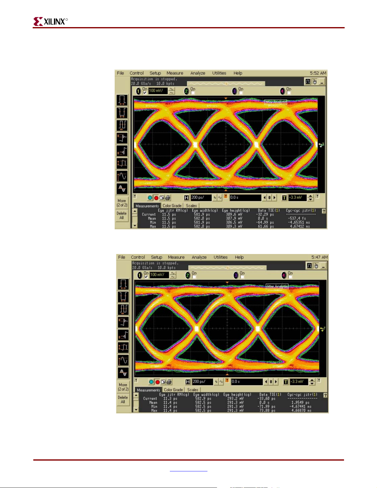
R
Chapter 2: Using the System
transmission using 0.5 meter and 1.0 meter SATA cables are shown in Figure 2-21.and
Figure 2-22.
Figure 2-21: 1.5 Gb/s Serial Data Transmission over 0.5 meter of SATA Cable
Figure 2-22: 1.5 Gb/s Serial Data Transmission over 1.0 meter of SATA Cable
70 www.xilinx.com XUP Virtex-II Pro Development System
UG069 (v1.0) March 8, 2005
Page 71

R
Appendix A
Configuring the FPGA from the Embedded USB Configuration Port
The XUP Virtex-II Pro Development System contains an embedded version of the Platform
Cable USB for the purpose of configuration and programming the Virtex-II Pro FPGA and
the Platform FLASH PROM using an off-the-shelf high-speed USB A-B cable.
Configuration and programming are supported by iMPACT (v6.3.01i or later) download
software using Boundary Scan (IEEE 1149.1/IEEE 1532) mode. Target clock speeds are
selectable from 750 kHz to 24 MHz.
The host computer must contain a USB host controller with one or more USB ports. The
controller can reside on the mother board or can be added using an expansion card or
PCMCIA/CARDBUS adapter.
The host operating system must be either Windows 2000 (SP4 or later) or Windows XP (SP1
or later). IMPACT v6.3.01I and ChipScope Pro are not supported by earlier versions of
Windows.
The embedded Platform Cable USB interface is designed to take full advantage of the
bandwidth of USB 2.0 ports. It is also backward compatible with USB 1.1 ports. The
interface is self-powered and consumes no power from the host hub. It is enumerated as a
high-speed device on USB 2.0 hubs or a full-speed device on USB 1.1 hubs.
A proprietary Windows device driver is required to use the embedded Platform Cable
USB. All Foundation ISE software releases and service packs beginning with version
6.3.01i incorporate this device driver. Windows does not recognize the embedded Platform
Cable USB until the appropriate Foundation ISE or ChipScope Pro installation has been
completed.
The embedded Platform Cable USB is a RAM-based product. Application code is
downloaded each time the cable is detected by the host operating system. USB protocol
guarantees that the application code is successfully transmitted. All necessary firmware
files are included with every Foundation ISE software installation CD. Revised firmware
can be periodically distributed in subsequent software releases.
The embedded Platform Cable USB can be attached and removed from the host computer
without the need to power-down or reboot the host computer. When the embedded
Platform Cable is detected by the operating system, a “Programming Cables” folder is
displayed if the System Properties -> Hardware -> Device Manager dialog box is selected.
A “Xilinx Platform Cable USB” entry resides in this folder as shown in Figure A-1.
XUP Virtex-II Pro Development System www.xilinx.com 71
UG069 (v1.0) March 8, 2005 1-800-255-7778
Page 72

R
Appendix A: Configuring the FPGA from the Embedded USB Configuration Port
Figure A-1: Device Manager Cable Entry
There is no difference between the embedded Platform Cable USB implementation and the
standalone Platform Cable USB hardware. The host computer operating system and
iMPACT reports the attached cable as the standalone version.
The embedded Platform Cable USB can be designated as the “active” configuration cable
by selecting “Output -> Cable Setup” from the iMPACT tool bar as shown in Figure A-2.
Figure A-2: iMPACT Cable Selection Drop-Down Menu
72 www.xilinx.com XUP Virtex-II Pro Development System
1-800-255-7778 UG069 (v1.0) March 8, 2005
Page 73

When the Cable Communications Setup dialog box is displayed, the Communications
Mode radio button must be set to Platform Cable USB as shown in Figure A-3. If no USB
host is available, then select Parallel IV, attach a PC4 cable to J27.
Figure A-3: iMPACT Cable Communication Setup Dialog
R
Regardless of the native communications speed of the host USB port, target devices can be
clocked at any of six different frequencies by making the appropriate selection in the TCK
Speed/Baud Rate drop-down list.
The default clock rate of 6 MHz is selected by iMPACT, because all Xilinx devices are
guaranteed to be programmed at that rate. The basic XUP Virtex-II Pro Development
System contains a Platform FLASH PROM and a Virtex-II Pro FPGA. This combination of
devices does not support the maximum JTAG TCK clock frequency. This means that the
TCK Speed/Baud Rate could be set to 12 MHz. If expansion circuit boards that contain
programmable devices are added to the basic system, the user must ensure that the JTAG
clock frequency does not exceed the capability of the additional devices.
XUP Virtex-II Pro Development System www.xilinx.com 73
UG069 (v1.0) March 8, 2005 1-800-255-7778
Page 74

R
Appendix A: Configuring the FPGA from the Embedded USB Configuration Port
After the programming cable type and speed has been selected, the JTAG chain must be
defined. Right click in the iMPACT window and select “Initialize Chain” from the dropdown menu shown in Figure A-4.
Figure A-4: Initializing the JTAG Chain
A status bar on the bottom edge of the iMPACT GUI provides useful information about the
operating conditions of the software and the attached cable. If the host port is USB 1.1,
Platform Cable USB connects at full-speed, and the status bar shows “usb-fs.” If the host
port is USB 2.0, Platform Cable USB connects at high-speed and the status bar shows “usbhs.” The active JTAG TCK speed is shown in the right-hand corner of the status bar.
Figure A-4, shows a Platform Cable USB connected at high-speed, using a Boundary-Scan
Configuration Mode with a JTAG TCK of 12 MHz.
If there are no configurable expansion boards attached to the basic system, the Initialize
Chain command should identify three devices in the chain: the Platform FLASH PROM
(XCF32P), followed by the System ACE controller (XCCACE), and followed by the FPGA
(XC2VP30). Any programmable devices on expansion boards follow the FPGA in the
configuration chain. A properly identified JTAG configuration chain for the basic system is
shown in Figure A-5.
74 www.xilinx.com XUP Virtex-II Pro Development System
1-800-255-7778 UG069 (v1.0) March 8, 2005
Page 75

Figure A-5: Properly Identified JTAG Configuration Chain
Right click on each of the devices in the chain and select “Assign New Configuration File”
from the drop-down menu (see Figure A-6). The Platform FLASH PROM and the System
ACE controller should be set to BYPASS, and the desired configuration file for the FPGA
should be specified as shown in Figure A-7.
R
Figure A-6: Assigning Configuration Files to Devices in the JTAG Chain
XUP Virtex-II Pro Development System www.xilinx.com 75
UG069 (v1.0) March 8, 2005 1-800-255-7778
Page 76

R
Appendix A: Configuring the FPGA from the Embedded USB Configuration Port
Figure A-7: Assigning a Configuration File to the FPGA
Any additional files required by the design can specified at this time. Right click on the
Virtex-II Pro FPGA and select “Program” to program the device as shown in Figure A-8.
Figure A-8: Programming the FPGA
76 www.xilinx.com XUP Virtex-II Pro Development System
1-800-255-7778 UG069 (v1.0) March 8, 2005
Page 77

R
Appendix B
Programming the Platform FLASH PROM User Area
The XUP Virtex-II Pro Development System contains an XCF32P Platform FLASH PROM
that is used to contain a known “Golden” configuration and a separate “User”
configuration. These two FPGA configurations are supported by the design revisioning
capabilities of the Platform FLASH PROMs. The “Golden” configuration is stored in
Revision 0 and is write/erase protected, and the “User” configuration is stored in
Revision 1.
Programming the XCF32P Platform FLASH PROM is supported by iMPACT (v6.3.01i or
later) download software using Boundary Scan (IEEE 1149.1 /IEEE 1532) mode from either
the embedded Platform Cable USB (J8) or the PC4 cable connection (J27).
The.bit file created by the Xilinx implementation tools must be converted to an.MKS file
before it can be programmed into the Platform FLASH PROM.
1. Start iMPACT and select Prepare Configuration Files as shown in Figure B-1.
Figure B-1: Operation Mode Selection: Prepare Configuration Files
XUP Virtex-II Pro Development System www.xilinx.com 77
UG069 (v1.0) March 8, 2005 1-800-255-7778
Page 78

R
Appendix B: Programming the Platform FLASH PROM User Area
2. Click on Next and select PROM File in the Prepare Configuration Files option menu
shown in Figure B-2.
Figure B-2: Selecting PROM File
3. Click on Next and then select Xilinx PROM with Design Revisioning Enabled using the
MCS PROM File Format.
4. Give the PROM File a name of your choice in the location of your choice as shown in
Figure B-3.
Note:
hardware does not support this option.
Do NOT select Compress Data, because the XUP Virtex-II Pro Development System
78 www.xilinx.com XUP Virtex-II Pro Development System
1-800-255-7778 UG069 (v1.0) March 8, 2005
Page 79

R
Figure B-3: Selecting a PROM with Design Revisioning Enabled
5. Click on Next to bring up the option screen where the type of PROM is specified.
6. Select the XCF32P PROM from the drop down men. Click on the “Add” button and
specify “2” from the Number of Revisions drop down menu as shown in Figure B-4.
Figure B-4: Selecting an XCF32P PROM with Two Revisions
XUP Virtex-II Pro Development System www.xilinx.com 79
UG069 (v1.0) March 8, 2005 1-800-255-7778
Page 80
R
Appendix B: Programming the Platform FLASH PROM User Area
7. Click on Next twice to bring up the Add Device File screen shown in Figure B-5.
Figure B-5: Adding a Device File
8. Click on Add File and navigate to your design directory and select the.bit file for your
design as shown in Figure B-6.
9. Click on Open and answer No when prompted to add another design file to
Revision 0.
Figure B-6: Adding the Design File to Revision 0
80 www.xilinx.com XUP Virtex-II Pro Development System
1-800-255-7778 UG069 (v1.0) March 8, 2005
Page 81
10. Note that Revision 0 is highlighted in green; this is where the “Golden” configuration
will be placed in the PROM. By selecting your design file for Revision 0, you are just
reserving space in the PROM for the “Golden” configuration. Your design file will not
overwrite the “Golden” configuration because it is write/erase protected.
If the design file was created with the Startup Clock set to JTAG, iMPACT will issue a
warning that the Startup Clock will be changed to CCLK in the bitstream programmed
into the PROM. This warning is shown in Figure B-7 and can be safely ignored.
Figure B-7: iMPACT Startup Clock Warning
11. Once you answer No when prompted to add another design file to Revision 0, the
green revision highlight will move to Revision 1. You will be prompted to add your
design file to Revision 1 as shown in Figure B-8.
R
Figure B-8: Adding the Design File to Revision 1
12. Click on Open and answer No when prompted to add another design file to
Revision 1. Click on Finish to start the generation of the MCS file as shown in
Figure B-9.
XUP Virtex-II Pro Development System www.xilinx.com 81
UG069 (v1.0) March 8, 2005 1-800-255-7778
Page 82
R
Appendix B: Programming the Platform FLASH PROM User Area
Figure B-9: Generating the MCS File
13. When prompted to compress the file, respond No, because the XUP Virtex-II Pro
Development System hardware does not support this option.
14. After iMPACT successfully creates the MCS file, select Configuration Mode from the
Mode menu as shown in Figure B-10.
Figure B-10: Switching to Configuration Mode
15. Make sure that the XUP Virtex-II Pro Development System is powered up and that
either a USB cable or a PC4 cable connects the board to the PC that is running the
iMPACT software.
16. Select the Initialize Chain command shown in Figure B-11.
82 www.xilinx.com XUP Virtex-II Pro Development System
1-800-255-7778 UG069 (v1.0) March 8, 2005
Page 83

Figure B-11: Initializing the JTAG Chain
The iMPACT software then interrogates the system and reports that there are at least
three devices in the JTAG chain. The first device is the XCF32P PROM; the second
device is the System ACE controller; and the third device is the Virtex-II Pro FPGA.
Any additional devices shown in the JTAG chain will reside on optional expansion
boards.
17. Select the MCS file that you created earlier as the configuration file for the XCF32P
PROM and click Open, as shown inFigure B-12.
R
Figure B-12: Assigning the MCS File to the PROM
18. Select BYPASS as the configuration files for the System ACE controller and the
Virtex-II Pro FPGA.
XUP Virtex-II Pro Development System www.xilinx.com 83
UG069 (v1.0) March 8, 2005 1-800-255-7778
Page 84

R
Appendix B: Programming the Platform FLASH PROM User Area
19. Right mouse click on the icon for the XCF32P PROM and select Program from the drop
down menu as shown in Figure B-13.
Figure B-13: Programming the PROM
20. The iMPACT software responds with a form that allows the user to specify which
design revisions are to be programmed and the programming options for the various
revisions. De-select Design Revision Rev 0 and all of the options for Design Revision
Rev 0 to minimize the programming time. Any options that you set for Design
Revision Rev 0 are ignored, because Design Revision Rev 0 has been previously
Erase/Write protected.
21. Select Design Revision Rev 1, and set the Erase (ER) bit to erase any previous “User”
design. Make sure that the Write Protect (WP) bit is not set.
22. Verify that the Operating Mode is set to Slave and the I/O Configuration is set to
Parallel Mode as shown in Figure B-14.
84 www.xilinx.com XUP Virtex-II Pro Development System
1-800-255-7778 UG069 (v1.0) March 8, 2005
Page 85
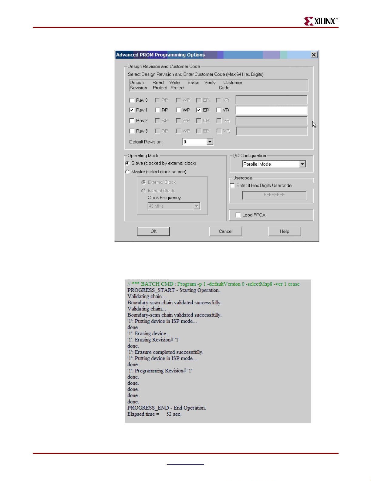
R
Figure B-14: PROM Programming Options
23. Click on OK to begin programming the PROM. The iMPACT transcript window shows
the sequence of operations that took place and looks similar to Figure B-15.
Figure B-15: iMPACT PROM Programming Transcript Window
XUP Virtex-II Pro Development System www.xilinx.com 85
UG069 (v1.0) March 8, 2005 1-800-255-7778
Page 86

R
Appendix B: Programming the Platform FLASH PROM User Area
24. To load the newly programmed PROM configuration file into the Virtex-II Pro FPGA,
verify that the “CONFIG SOURCE” switch is set to enable high-speed SelectMap bytewide configuration from the on-board Platform Flash configuration PROM, and that
the “PROM VERSION” switch is set to enable the “User” configuration. If the switches
are set properly, only the green “PROM” LED (D19) is illuminated.
25. Press the “RESET\RELOAD” push button until the red “RELOAD” turns on. Release
the push button and the new “User” configuration is transferred to the FPGA.
86 www.xilinx.com XUP Virtex-II Pro Development System
1-800-255-7778 UG069 (v1.0) March 8, 2005
Page 87

R
Restoring the Golden FPGA Configuration
The XUP Virtex-II Pro Development System contains an XCF32P Platform FLASH PROM
that is used to contain a known Golden configuration and a separate User configuration.
These two FPGA configurations are supported by the design revisioning capabilities of the
Platform FLASH PROMs. The Golden configuration is stored in Revision 0 and is
write/erase protected, and the User configuration is stored in Revision 1.
Programming of the XCF32P Platform FLASH PROM is supported by iMPACT (v6.3.01i or
later) download software using Boundary Scan (IEEE 1149.1 /IEEE 1532) mode from either
the embedded Platform Cable USB (J8) or the PC4 cable connection (J27).
Appendix C
The latest Golden configuration file can be obtained from the XUP Virtex-II Pro
Development System support Web site at: http://www.xilinx.com/univ/xup2vp.html
This configuration file is used to verify the proper operation of the complete system.
1. Download the XUP_V2Pro_BIST.zip file and extract the files to a directory of your
choice. The ZIP file contains two files:
♦ XUP_V2Pro_BIST.mcs, the data file that will be loaded into the PROM, and
♦ XUP_V2Pro_BIST.cfi, a file that describes the design revision structure in the
PROM.
2. Make sure that the XUP Virtex-II Pro Development System is powered up and that
either a USB cable or a PC4 cable connects the board to the PC that is running the
iMPACT software.
.
Xilinx University Program Virtex-II Pro Development Systemwww.xilinx.com 87
UG069 (v1.0) March 8, 2005 1-800-255-7778
Page 88
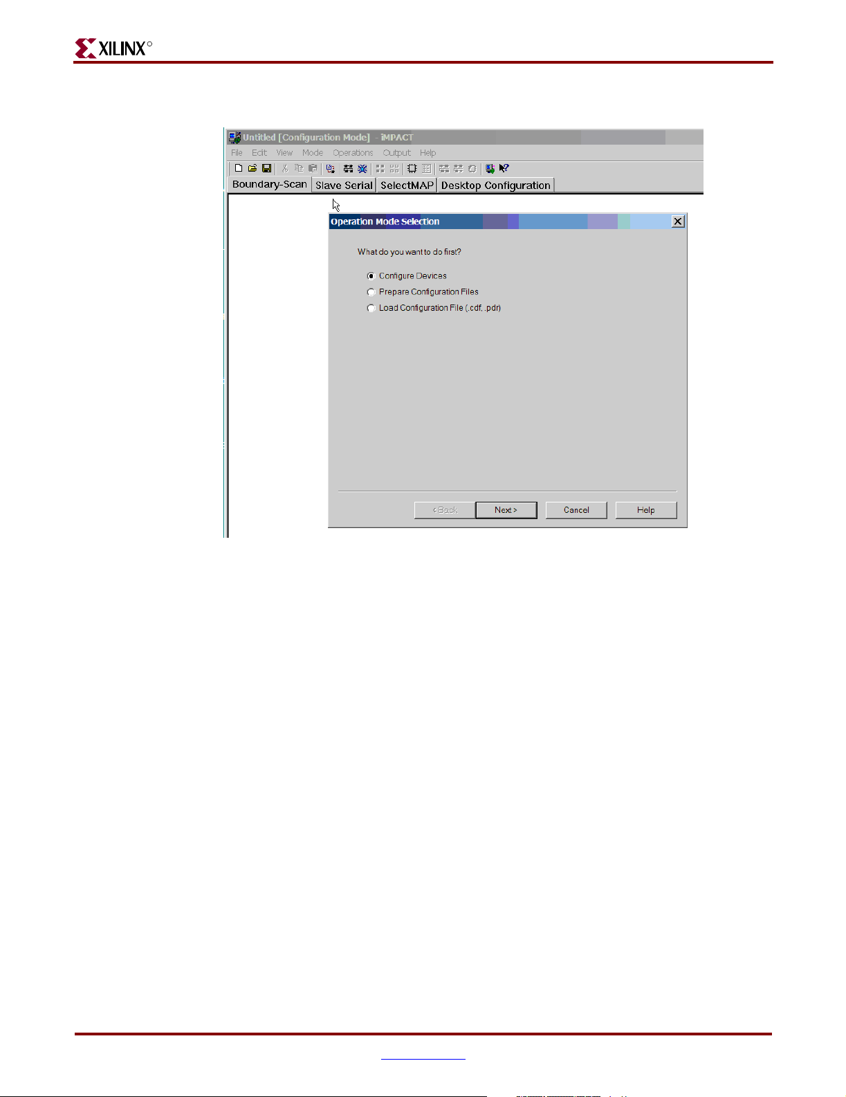
R
Appendix C: Restoring the Golden FPGA Configuration
3. Start up iMPACT and select Configure Devices as shown in Figure C-1.
Figure C-1: Operation Mode Selection: Configure Devices
4. Clock on Next and select the Boundary Scan Mode from the option menu shown in
Figure C-2.
88 www.xilinx.comXilinx University Program Virtex-II Pro Development
System
1-800-255-7778 UG069 (v1.0) March 8, 2005
Page 89
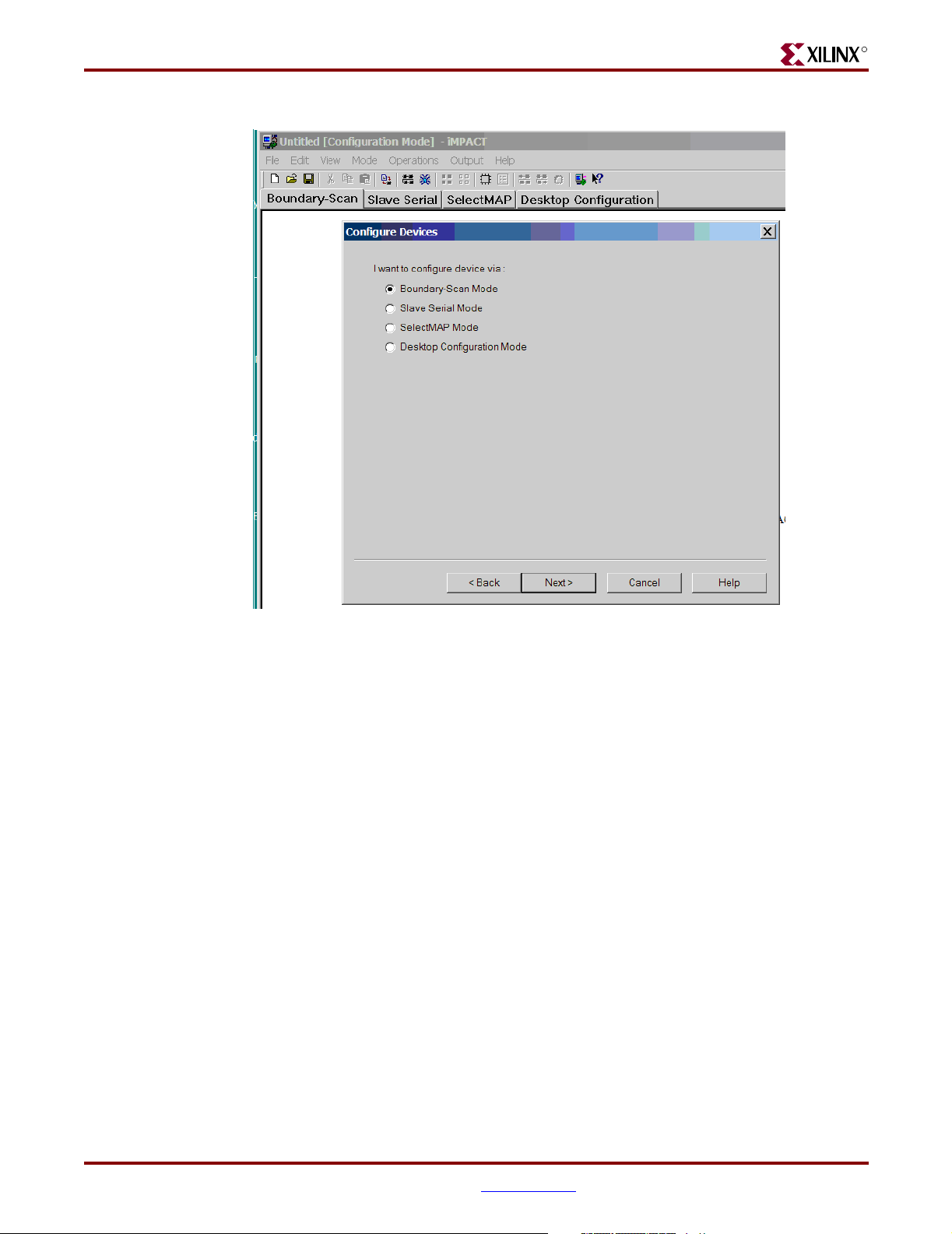
R
Figure C-2: Selecting Boundary Scan Mode
Xilinx University Program Virtex-II Pro Development Systemwww.xilinx.com 89
UG069 (v1.0) March 8, 2005 1-800-255-7778
Page 90

R
Appendix C: Restoring the Golden FPGA Configuration
5. Click on Next and then select Automatically connect to the cable and identify the
Boundary Scan as shown in Figure C-3.
Figure C-3: Boundary Scan Mode Selection: Automatically Connect to the Cable
and Identify the JTAG Chain
6. Click on Finish and the iMPACT software then interrogates the system and reports that
there are at least three devices in the JTAG chain. The first device is the XCF32P PROM,
the second device is the System ACE controller, and the third device is the Virtex-II Pro
FPGA. Any additional devices shown in the JTAG chain reside on optional expansion
boards.
7. Navigate to the directory where you saved the XUP_V2Pro_BIST.mcs file. Select this
file as the Configuration file for the XCF32P PROM, the first device in the JTAG chain
identified by iMPACT as shown in Figure C-4. Click on the Open button.
90 www.xilinx.comXilinx University Program Virtex-II Pro Development
System
1-800-255-7778 UG069 (v1.0) March 8, 2005
Page 91
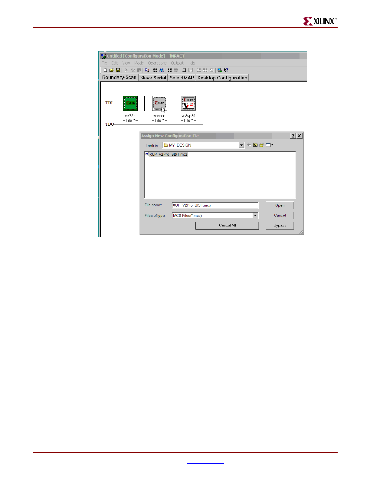
R
Figure C-4: Assigning New PROM Configuration File
8. Select BYPASS as the configuration files for the System ACE controller and the VirtexII Pro FPGA.
9. Right mouse click on the icon for the XCF32P PROM and select Erase from the drop
down menu as shown in Figure C-5. When the erase options screen appears, select All
Revisions and then click OK.
Xilinx University Program Virtex-II Pro Development Systemwww.xilinx.com 91
UG069 (v1.0) March 8, 2005 1-800-255-7778
Page 92

R
Appendix C: Restoring the Golden FPGA Configuration
Figure C-5: Erasing the Existing PROM Contents
The iMPACT software then erases the complete contents of the PROM, including old
versions of the Golden and User designs. The transcript window should look similar to
Figure C-6.
Figure C-6: Transcript Window for the Erase Command
10. Right mouse click on the icon for the XCF32P PROM and select Program from the drop
down menu as shown in Figure C-7.
92 www.xilinx.comXilinx University Program Virtex-II Pro Development
System
1-800-255-7778 UG069 (v1.0) March 8, 2005
Page 93

R
Figure C-7: Selecting the Program Command
11. The iMPACT software responds with a form that allows the user to specify which
design revisions are to be programmed and the programming options for the various
revisions. Select Design Revision Rev 0 and set the Write Protect (WP) bit to prevent
the user from overwriting the Golden configuration. Verify that the Operating Mode is
set to Slave and the I/O Configuration is set to Parallel Mode as shown in Figure C-8.
Xilinx University Program Virtex-II Pro Development Systemwww.xilinx.com 93
UG069 (v1.0) March 8, 2005 1-800-255-7778
Page 94

R
Appendix C: Restoring the Golden FPGA Configuration
Figure C-8: PROM Programming Options
12. Click on OK to begin programming the PROM. The iMPACT transcript window shows
the sequence of operations that took place and looks similar to Figure C-9.
94 www.xilinx.comXilinx University Program Virtex-II Pro Development
System
1-800-255-7778 UG069 (v1.0) March 8, 2005
Page 95

Figure C-9: iMPACT PROM Programming Transcript Window
13. To load the newly programmed PROM configuration file into the Virtex-II Pro FPGA,
verify that the CONFIG SOURCE switch is set to enable high speed SelectMap byte
wide configuration from the on-board Platform Flash configuration PROM and that
the PROM VERSION switch is set to enable the Golden configuration. If the switches
are set properly, the green PROM CONFIG LED (D19) and the amber GOLDEN
GONFIG LED (D14) are illuminated.
14. Press the RESET\RELOAD push button until the red RELOAD turns on. Upon
releasing the push button, the new Golden configuration is transferred to the FPGA.
R
Xilinx University Program Virtex-II Pro Development Systemwww.xilinx.com 95
UG069 (v1.0) March 8, 2005 1-800-255-7778
Page 96

R
Appendix C: Restoring the Golden FPGA Configuration
96 www.xilinx.comXilinx University Program Virtex-II Pro Development
System
1-800-255-7778 UG069 (v1.0) March 8, 2005
Page 97
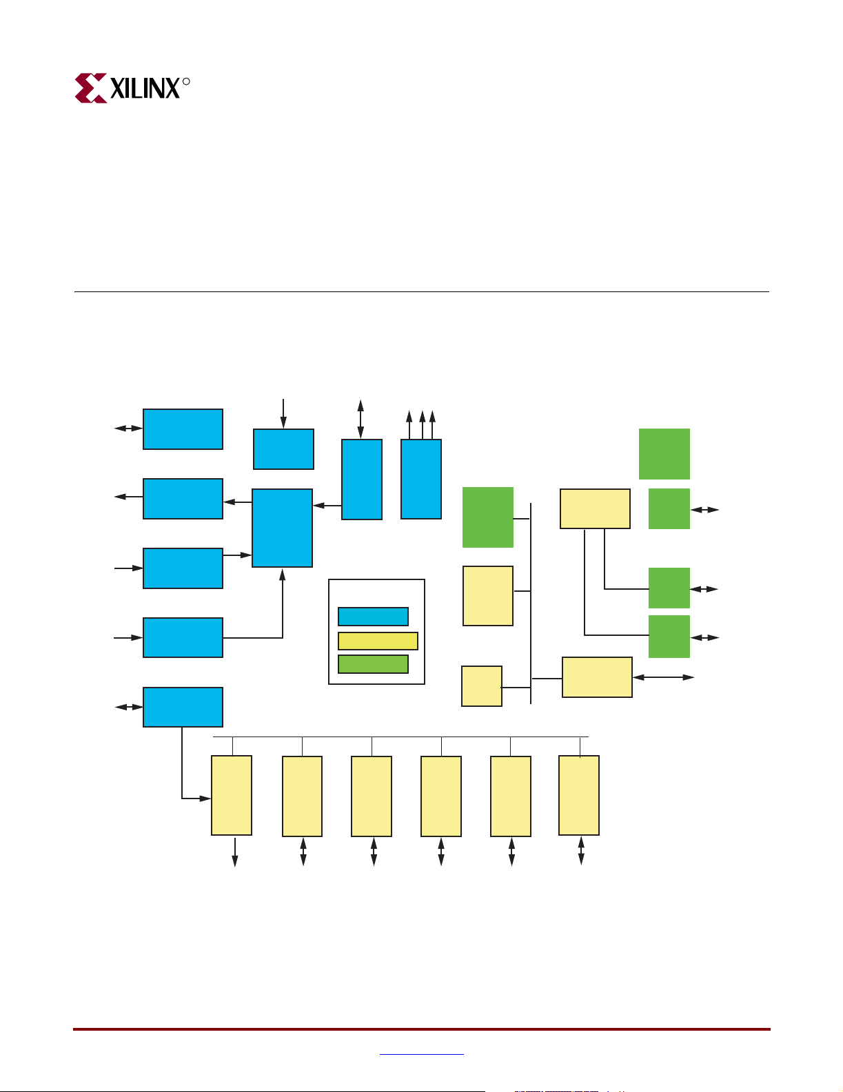
R
Appendix D
Using the Golden FPGA Configuration for System Self-Test
A special design has been placed in the Platform FLASH PROM to provide a Built-in SelfTest (BIST) boot/configuration that tests critical board features and reports on board health
and status. Figure D-1 shows BIST block diagram.
Audio Tones &
Push Buttons
Clock
Generator
PPC 1
VGA
Keyboard
PS2
LEDs &
DIP Switches
Generator
GPIO
Char. &
Test
Pattern
II C
HARDWARE
PROC PERIPH
CNTRL
Silicon
Ser Number
Key
HARD IP
OPB BUS
AC 97
CNTRL
Por t Test
External
ETHERNET
MAC
PPC 0
BRAM
128 Kb
Bridge
PLB
BUS
SYSACE
DDR SDRAM
CONTROL
CONTRL
Figure D-1: XUP Virtex-II Pro Development System BIST Block Diagram
PLB AT
LITE
LITE
UART
UART
MGT
MGT
MGT
UG069_20_010605
Appendix C, “Restoring the Golden FPGA Configuration,” of this document covers the
details of restoring the BIST design if it has been erased accidentally. This feature puts the
board through several tests to verify the board is fully functional in a stand-alone
environment. Other tests to verify system-level functionality can be supported via
XUP Virtex-II Pro Development System www.xilinx.com 97
UG069 (v1.0) March 8, 2005 1-800-255-7778
Page 98

R
Compact Flash or download, but the “Golden Boot” has been designed to verify that the
board is not damaged due to user abuse. This mode allows the user to verify that the board
itself is not the root cause of a design failing to function properly.
The BIST is a combination of pure hardware and processor centric tests combined into one
FPGA design.
The “Golden Boot” design covers the following elements of the system:
1. Clock presence
2. Push buttons, DIP switches, and LEDs
3. Audio CODEC and power amplifier
4. RS-232 serial ports and PS/2 ports
5. SVGA output
6. 10/100 Ethernet and Silicon Serial Number
7. Expansion ports
8. MGTs
9. System ACE processor interface
10. DDR SDRAM module and Serial Presence Detect PROM
Appendix D: Using the Golden FPGA Configuration for System Self-Test
The BIST consists of two different test strategies, a series of processor centric tests and pure
hardware non-processor centric tests. The pure hardware tests are used to verify the most
basic functions of the system and to provide a platform on which the processor centric tests
can build.
Hardware-Based Tests
These tests should be run in the order listed, because each test design can require a positive
result from a previous test.
Power Supply and RESET Test
This test verifies the correct operation of the on-board power supplies and system RESET
generation circuitry.
Additional Hardware Required
• 5V external power supply
• Multimeter
• Shorting Jumper Block
Test Procedure
1. Verify that three Shorting Jumper Blocks are installed in JP1, JP2, and JP3
2. Plug in the external 5V power supply, and turn on the board by sliding SW11 up
towards the “ON” label.
3. Connect the negative lead of the multimeter to J31 and the positive lead to J30. The
meter should read between 2.375V and 2.625V, and LED D17 “2.5V OK” should be on.
4. Connect the negative lead of the multimeter to J33 and the positive lead to J32. The
meter should read between 3.135V and 3.465V, and LED D18 “3.3V OK” should be on.
98 www.xilinx.com XUP Virtex-II Pro Development System
1-800-255-7778 UG069 (v1.0) March 8, 2005
Page 99

Hardware-Based Tests
Clock, Push Button, DIP Switch, LED, and Audio Amp Test
R
5. Connect the negative lead of the multimeter to J35 and the positive lead to J34. The
meter should read between 1.425V and 1.575V, and LED D19 “1.5V OK” should be on.
6. Install the Shorting Jumper Block on JP2, LED D17 “2.5V OK” should be off, and D6
“RELOAD PS ERROR” should be on. Remove the Shorting Jumper Block.
7. Install the Shorting Jumper Block on JP6, LED D19 “1.5V OK” should be off, and D6
“RELOAD PS ERROR” should be on. Remove the Shorting Jumper Block.
8. Turn the circuit board over.
9. Connect the negative lead of the multimeter to the negative side of C433 and the
positive lead to the positive side of C433. The meter should read between 2.375V and
2.625V, verifying the correct voltage for the MGT termination.
10. Connect the negative lead of the multimeter to the negative side of C428 and the
positive lead to the positive side of C428. The meter should read between 2.375V and
2.625V, verifying the correct voltage for the MGT power supply.
11. Turn the circuit board component side up.
This test verifies the presence of the various clocks, push buttons, DIP switches, audio
amplifier, and the beep-tone passthrough capability of the audio CODEC. The four user
LEDs are used to verify the operation of the clocks and to display the status of the user DIP
switches. Pressing each of the push buttons results in a different tone from the headphones.
Additional Hardware Required
• 5V external power supply
• Headphones
Test Procedure
1. Set the “CONFIG SOURCE/PROM VERSION” DIP switch SW9 with both of the
switches up or closed.
2. Plug in the external 5V power supply, and turn on the board by sliding SW11 up
towards the “ON” label. LEDs D14 “GOLDEN CONFIG”, D19 “PROM CONFIG,” and
D4 “DONE” should be on.
3. Observe the status of the four user LEDs: D7-10. LED 3, LED 2, and LED1 should flash
at different rates, and LED 0 should be on steady indicating that the DCMs in the
FPGA are locked to the clock signals.
♦ A flashing LED 3 indicates that the 100 MHz system clock is present.
♦ A flashing LED 2 indicates that the 75 MHz MGT clock is present.
♦ A flashing LED 1 indicates that the 32 MHz System ACE clock is present.
♦ A steady-on LED 0 indicates that the DCMs are locked.
4. After about 5 seconds, the LEDs should shop flashing and their function changes to
indicate the status of the USER INPUT DIP switch SW7. If a switch is down or open,
the corresponding LED will be off, if the switch is up or closed the LED will be on.
♦ LED 3 shows the status of USER INPUT switch 3.
♦ LED 2 shows the status of USER INPUT switch 2.
♦ LED 1 shows the status of USER INPUT switch 1.
♦ LED 0 shows the status of USER INPUT switch 0.
XUP Virtex-II Pro Development System www.xilinx.com 99
UG069 (v1.0) March 8, 2005 1-800-255-7778
Page 100

R
5. Briefly (less than 2 seconds), press the “RESET/RELOAD” push button SW1. This
should result in the LEDs displaying the clock status again for 5 seconds.
6. Connect the headphones to the upper jack of J14 “AMP OUT.”
Warning:
LOUD.
7. Press each one of the push buttons, SW2-6. A different tone will be produced as each
push button is pressed.
Appendix D: Using the Golden FPGA Configuration for System Self-Test
Do not put the headphones on your ears, because the tones generated will be
SVGA Gray Scale Test
This test verifies the operation of the video DAC by creating a gray scale ramp that drives
each of the red, green, and blue channels with the same signal. Any color present indicates
the failure of one or more channel outputs. Any data bus errors will show up as
discontinuities in the ramp. There should be 1.5 ramps visible on the display.
Additional Hardware Required
• 5V external power supply
• SVGA display with cable capable of showing a 640 x 480 at 60 Hz image
Test Procedure
1. Set the “CONFIG SOURCE/PROM VERSION” DIP switch SW9 with both of the
switches up or closed.
2. Plug in the external 5V power supply and turn on the board by sliding SW11 up
towards the “ON” label. LEDs D14 “GOLDEN CONFIG,” D19 “PROM CONFIG,” and
D4 “DONE” should be on.
3. Connect the SVGA display to the SVGA output connector J13. A gray scale ramp
should be seen on the bottom of display.
SVGA Color Output Test
This test verifies the operation of the video DAC by creating a color bar pattern starting
with 100% white followed by 75% color bars. Between each of the color bars, there should
be a 2-pixel black stripe. This test makes sure that all color channels can be driven
individually and in-groups.
Additional Hardware Required
• 5V external power supply
• SVGA display with cable capable of showing a 640 x 480 at 60 Hz image
Test Procedure
1. Set the “CONFIG SOURCE/PROM VERSION” DIP switch SW9 with both of the
switches up or closed.
2. Plug in the external 5V power supply, and turn on the board by sliding SW11 up
towards the “ON” label. LEDs D14 “GOLDEN CONFIG,” D19 “PROM CONFIG,” and
D4 “DONE” should be on.
3. Connect the SVGA display to the SVGA output connector J13. Seven distinct color bars
should be visible in the middle of the display with a black stripe between each color.
100 www.xilinx.com XUP Virtex-II Pro Development System
1-800-255-7778 UG069 (v1.0) March 8, 2005
 Loading...