

Page 1

FMC-CE Hardware
User Guide
UG-FMC-CE (v1.1) August 23, 2010
Page 2
Date
Version
Revision
2/26/10
v0.9.0
Internal
d
raft
3/10/10
v1.0 First release
8/23/10
v1.1 UCFs updated to reflect changes in the FMC
-
CE board with additional verification
Xilinx is disclosing this user guide, manual, release note, and/or specification (the "Documentation") to you solely for use in the
development of designs to operate with Xilinx hardware devices. You may not reproduce, distribute, republish, download, display,
post, or transmit the Documentation in any form or by any means including, but not limited to, electronic, mechanical, photocopying,
recording, or otherwise, without the prior written consent of Xilinx. Xilinx expressly disclaims any liability arising out of your use of the
Documentation. Xilinx reserves the right, at its sole discretion, to change the Documentation without notice at any time. Xilinx
assumes no obligation to correct any errors contained in the Documentation, or to advise you of any corrections or updates. Xilinx
expressly disclaims any liability in connection with technical support or assistance that may be provided to you in connection with the
Information.
THE DOCUMENTATION IS DISCLOSED TO YOU “AS-IS” WITH NO WARRANTY OF ANY KIND. XILINX MAKES NO OTHER
WARRANTIES, WHETHER EXPRESS, IMPLIED, OR STATUTORY, REGARDING THE DOCUMENTATION, INCLUDING ANY
WARRANTIES OF MERCHANTABILITY, FITNESS FOR A PARTICULAR PURPOSE, OR NONINFRINGEMENT OF THIRD-PARTY
RIGHTS. IN NO EVENT WILL XILINX BE LIABLE FOR ANY CONSEQUENTIAL, INDIRECT, EXEMPLARY, SPECIAL, OR
INCIDENTAL DAMAGES, INCLUDING ANY LOSS OF DATA OR LOST PROFITS, ARISING FROM YOUR USE OF THE
DOCUMENTATION.
© 2009–2010 Xilinx, Inc. XILINX, the Xilinx logo, Virtex, Spartan, ISE, and other designated brands included herein are trademarks of
Xilinx in the United States and other countries. All other trademarks are the property of their respective owners.
Revision History
The following table shows the revision history for this document
i
Page 3

Contents
About This Guide ........................................................................................................................................................1
FMC-CE Card ...............................................................................................................................................................1
Overview .................................................................................................................................................................1
Features ..................................................................................................................................................................1
Appendix A: UCF for SP605 ..................................................................................................................................... 10
Appendix B: UCF for ML605 .................................................................................................................................... 13
Appendix C: VITA 57.1 FMC LPC (J63) and HPC (J64) Connector Pinout ................................................................. 18
Table of Tables
Table 1. Slide Switch FMC connections ......................................................................................................................2
Table 2. Linear LED Connections ................................................................................................................................3
Table 3. Button FMC Connections ..............................................................................................................................4
Table 4. FMC Connections for LEDs Adjacent to Push Buttons ..................................................................................5
Table 5. Rotary Switch FMC Connections ...................................................................................................................5
Table 6. LCD FMC Connections ...................................................................................................................................6
Table 7. Audio FMC Connections................................................................................................................................7
Table 8. SMA FMC Connections..................................................................................................................................7
Table 9. Leftmost PMOD FMC Connections ...............................................................................................................8
Table 10. Center PMOD FMC Connection ..................................................................................................................9
Table 11. Rightmost PMD FMC Connections ..............................................................................................................9
Table of Figures
Figure 1. FMC-CE Card with Features Annotated .......................................................................................................1
Figure 2. Slide Switch Schematics ...............................................................................................................................2
Figure 3. Schematic of LEDs for Both the Linear Array and Rosetta Array .................................................................3
Figure 4. Schematic for Buttons .................................................................................................................................4
Figure 5. Rotary Switch Schematic .............................................................................................................................5
Figure 6. SMA Schematics ..........................................................................................................................................7
ii
Page 4
About This Guide
The purpose is of this document is to convey the necessary information to the designer to successfully use the
capabilities of the FMC-CE I/O expansion card.
Each feature is independently described and contains a connection table. This table includes the name of the
signal, its location on the FMC, the voltage at which it must be programmed by the FPGA, and a brief description
of its function. Where the term “any” is provided, the FPGA may provide use voltage as the FPGAs signals are
passed directly to the device and not through any level shifter.
FMC-CE Card
Overview
The FMC-CE card is meant to be used with a Xilinx demonstration/evaluation board equipped with an FMC
connector. This board extends the I/O capabilities of the base platform and provides an I/O consistency among
various platforms.
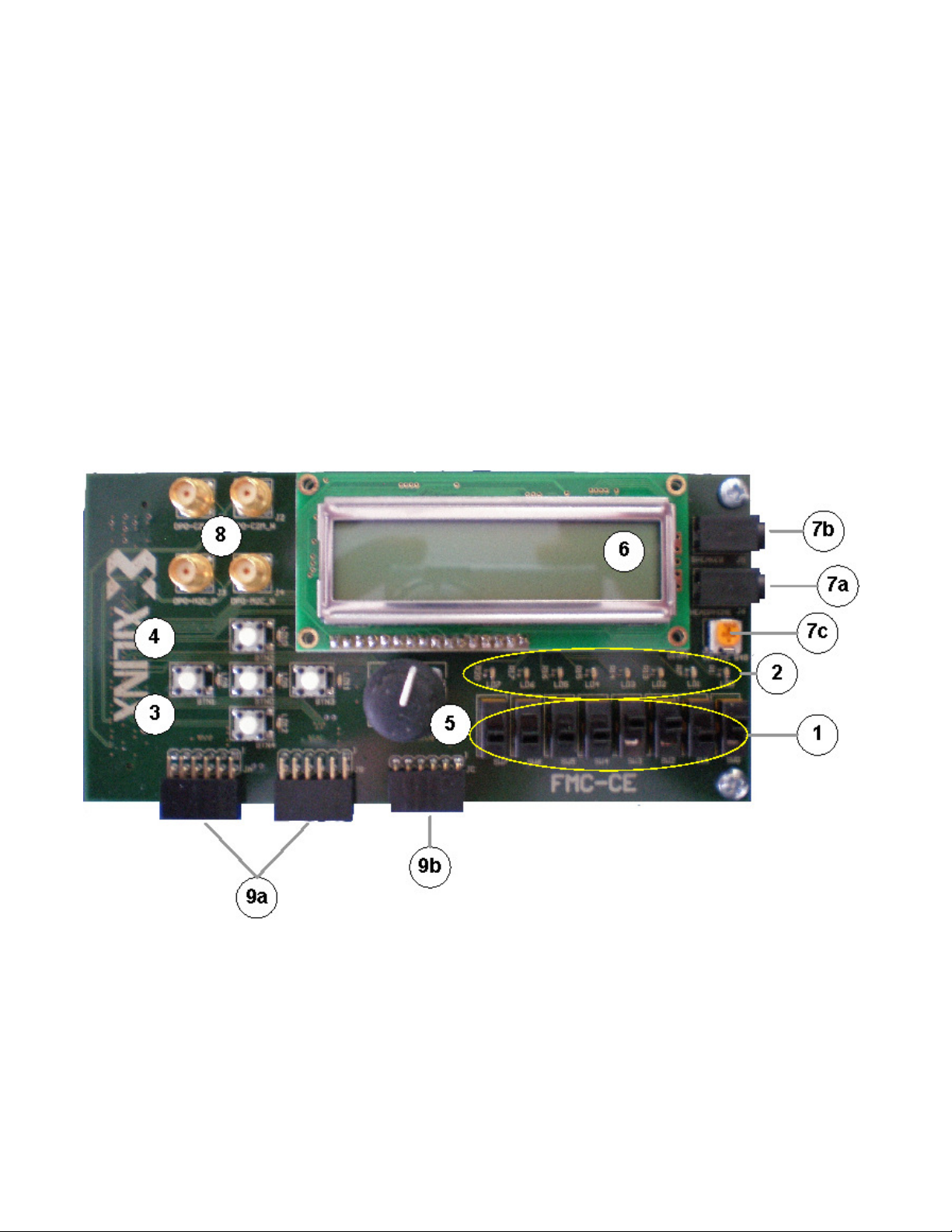
Figure 1. FMC-CE Card with Features Annotated
Features
The FMC-CE card provides the following features:
1) Linear array of 8 slide switches
2) Linear array of 8 LEDs co-located with the 8 slide switches
3) Rosetta pattern of 5 push button switches
1
Page 5
4) Rosetta pattern of 5 LEDs, co-located with the push button switches
Signal Name
Pin Voltage
Description
Switch 0
G33 ≤
2.5V
Switch 1
H32 ≤
2.5V
Switch 2
H31 ≤
2.5V
Switch 3
G31 ≤
2.5V
Switch 4
G30 ≤
2.5V
Switch 5
H29 ≤
2.5V
Switch 6
H28 ≤
2.5V
Switch 7
G28 ≤
2.5V
5) A Rotary/push-button switch
6) An LCD display (2x16).
7) Headphone jack (7a), speaker jack (7b) with a volume control (7c).
8) 4 SMA connectors
9) 2 Digilent dual PMOD connectors (9a), 1 Digilent single PMOD connector (9b)
Detailed Description
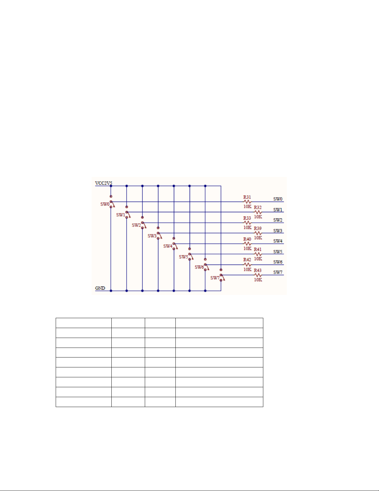
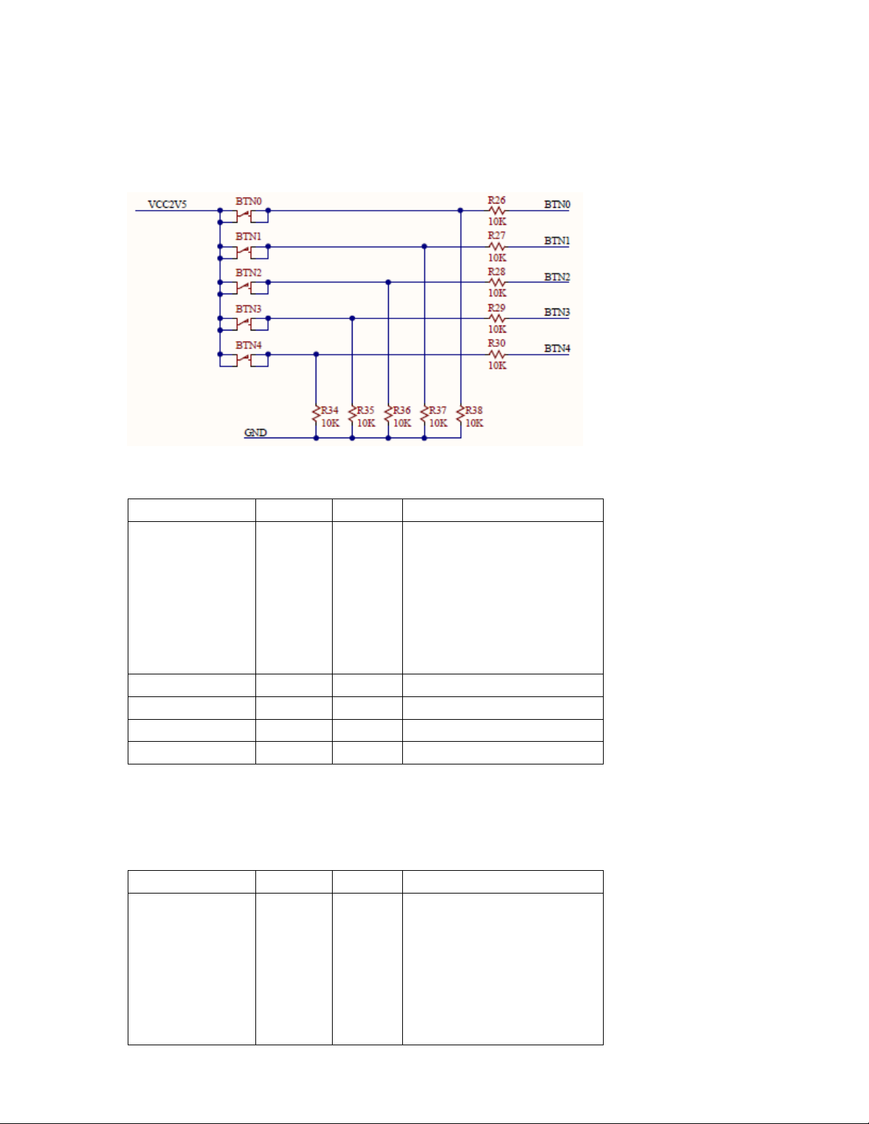
1. 8 Slide switches: One side of each of the eight slide switches is tied to GND, while the other side is pulled
up to 2.5V. There is a 10K series resistor for each switch which enables these signals to be used at lower
voltages without damaging the FPGA. These switches are silkscreened SW0-SW7. SW0 is on the right
most side.
Figure 2. Slide Switch Schematics
Table 1. Slide Switch FMC connections
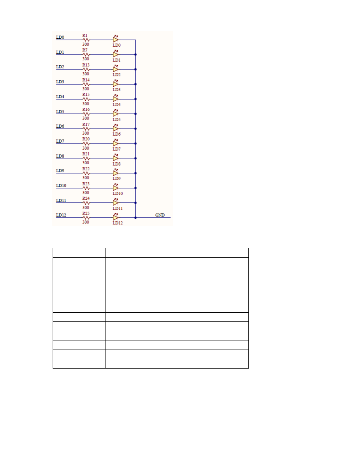
2. There are 8 LED's in a linear fashion, co-located with the slide switches. Each is tied to GND through a
300 Ohm resistor. LD0 is on the right most side. The LEDs illuminate with voltages as low as LVCMOS12.
2
Page 6
Signal Name
Pin Voltage
Description
LED linear 0
D27 any Voltage must be sufficient to
LED linear 1
D26 any
LED linear 2
C26 any
LED linear 3
D24 any
LED linear 4
D23 any
LED linear 5
C23 any
LED linear 6
C22 any
LED linear 7
D21 any
Figure 3. Schematic of LEDs for Both the Linear Array and Rosetta Array
cross the “on” threshold –
need to verify, as this might
be changed from “any” to >=
some voltage.
Table 2. Linear LED Connections
3
Page 7
Signal Name
Pin Voltage
Description
Button 0
H14 2.5V
Center
Button 1
G15 2.5V
West
Button 2
G18 2.5V
North
Button 3
H13 2.5V
East
Button 4
G12 2.5V
South
Signal Name
Pin Voltage
Description
LED Rosetta
0 H16 any Center
3. The 5 buttons are pulled to GND through a 10K resistor and pulled up to 2.5 V when pressed. When not
pressed the button is pulled up to 2.5V. A series resister (10K Ohms) bleeds off excess voltage if the
FPGA is programmed to an IO standard below 2.5V. These are marked BTN0-4.
Figure 4. Schematic for Buttons
Voltage must be sufficient to
cross the “on” threshold –
need to verify, as this might
be changed from “any” to >=
some voltage.
Table 3. Button FMC Connections
4. Then there are 5 LED's co-located with the buttons (BTN0-BTN4) in a Rosetta pattern. Each LED is pulled
to GND via a 300 Ohm resistor. The schematics are show in (2) Linear LEDs
Voltage must be sufficient to
cross the “on” threshold –
need to verify, as this might
be changed from “any” to >=
some voltage.
4
Page 8
Signal Name
Pin Voltage
Description
LED Rosetta 1
G16 any West
LED Rosetta 2
G19 any North
LED Rosetta 3
H17 any East
LED Rosetta 4
G13 any So
uth
Table 4. FMC Connections for LEDs Adjacent to Push Buttons
Signal Name
Pin Voltage
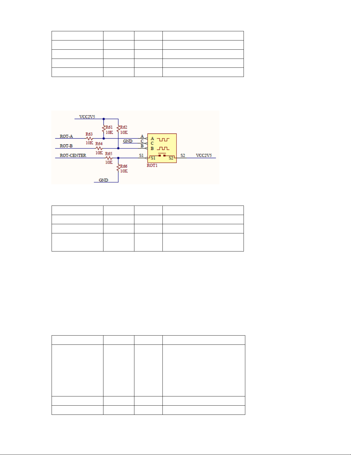
Description
Rot-A G21 2.5V
Reference w
aveform
Rot-B H19 2.5V
Quadrature waveform
Rot-Switch
H20 2.5V
Activated by pressing the
Signal Name
Pin Voltage
Description
LCD Data 0
G22 2.5V
LCD Data 1
H22 2.5V
As above
LCD Data 2
H23 2.5V
As above
5. Rotary Push-button LED linear labeled ROT-1
Figure 5. Rotary Switch Schematic
knob
Table 5. Rotary Switch FMC Connections
6. LCD (ST Micro ST7066) display with LVCMOS25 inputs. This dual row 16 character per row uses an
industry standard controller (Samsung KS0066U) and sports a 4 or 8 bit data interface. No backlight is
provided for the LCD, and the contrast if fixed.
This LCD supports 5x8 and 5x10 dot matrix characters and a programmable 4 or 8 bit MPU interface.
Support for custom characters is provided as is a wide range of instruction functions such as clear,
cursor home, display on/off, cursor shift, and display shift.
Four low order bi-directional
tristate data bus pins. Used for
data transfer and receive
between the MPU and the
ST7066.
These pins are not used during
4-bit operation.
5
Page 9
Signal Name
Pin Voltage
Description
LCD Data 3
G24 2.5V
As above
LCD Data 4
G25 2.5V
Four high order bi-directional
LCD Data 5
H25 2.5V
As above
LCD Data 6
H26 2.5V
As above
LCD Data 7
G27 2.5V
As above. Additionally DB7
LCD - RS
C19 2
.5V Register Select. 0: Instruction
LCD –
R/W
D20 2.5V
Read
(1)
/ Write
(0) control
LCD – E
C18 2.5V
Enable
-
Signal Name
Pin Voltage
Description
Audio DAC clo
ck left
H37 2.5V
30MHz max SPI
Audio DAC data left
G37 2.5V
16 bit frames
Audio DAC sync left
H38 2.5V
Marks start of data frame
Audio DAC clock right
H35 2.5V
30MHz max SPI
Audio DAC data right
H34 2.5V
16 bit frames
tristate data bus pins. Used for
data transfer and receive
between the MPU and the
ST7066.
can be used as a busy flag.
register (for write) and busy
flag and address counter for
read.
1: Data register for read and
write
Starts data read/write.
Table 6. LCD FMC Connections
7. Both the (a and b) stereo head set jack and a mono speaker jack are controlled via potentiometer
volume control (7c). Dual DAC121S101s (12-bit) digital to analog converters (DACs) provide stereo input
into a LM4838 2W Stereo Audio Amplifier. Each 12-bit DAC supports a data rate of up to 30MHz and is
compatible with SPI, QSPI, NICROWIRE, and DSP interfaces. The effective conversion rate is has a
conversion frequency of about 1.75MHz – well above the audio range. Both DAC outputs (right and left
channels) are then fed in the Audio Amplifier and are available through a mono speaker connector (left
channel only) on J5, and a stereo headphone connector on J6. Both output volumes are controlled via
the potentiometer R47, which is clearly labeled on the board.
Key specifications for part DAC121S101 from National Semiconductor:
DNL: +0.25, -0.15 LSB (typ)
Output Settling Time: 8 us (typ)
Zero Code Error: 4mV
Full Scale Error: -0.06%
6
Page 10
Signal Name
Pin Voltage
Description
Audio DAC sync right
G36 2.5V
Mar
ks start of data frame
Table 7. Audio FMC Connections
Signal Name
Pin Voltage
Description
SMA
-1 C2
any J1 –
north west
SMA
-2 C3
any J2 –
north east
SMA
-3 C6
any J3 –
south west
SMA
-4 C7
any J4 –
south east
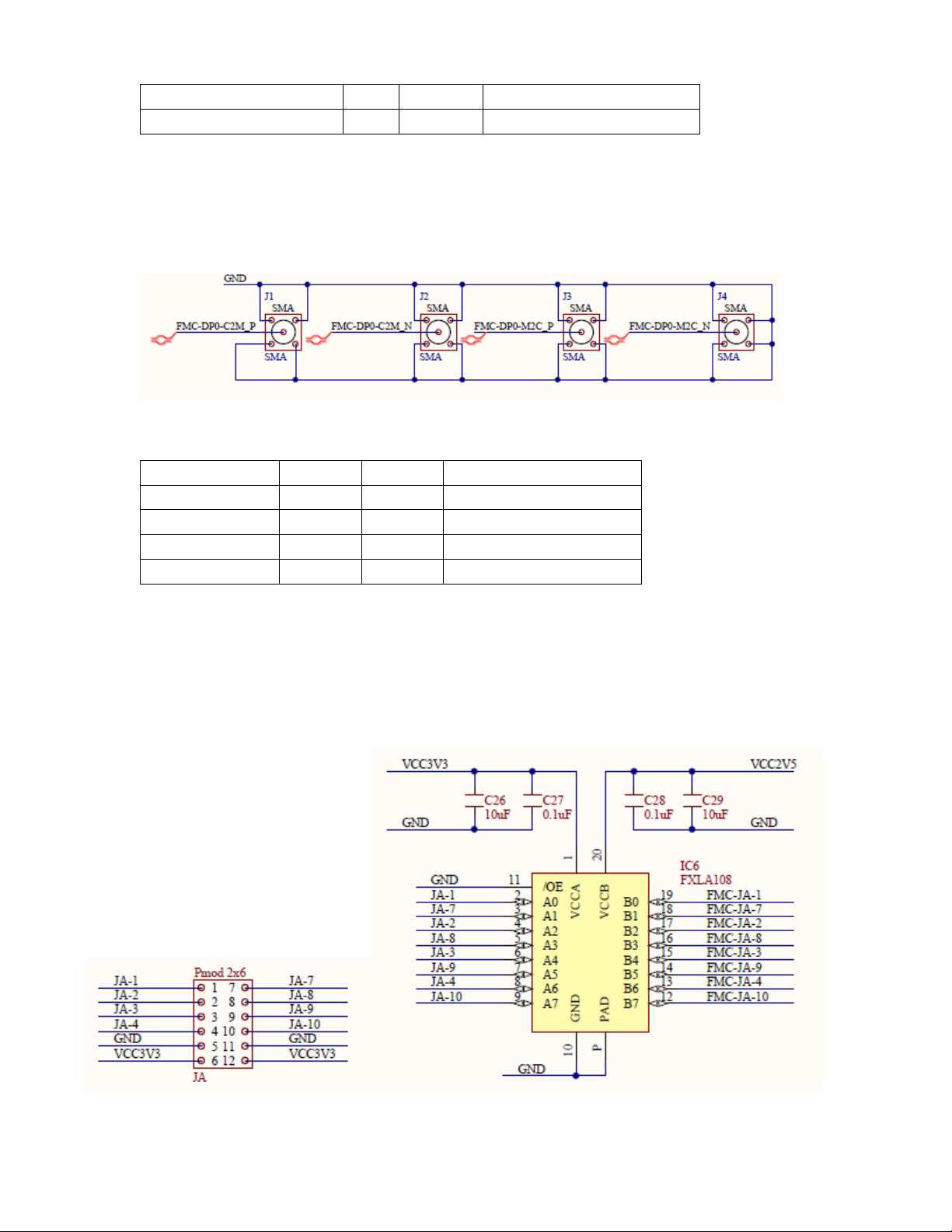
8. There are 4 SMA audio connectors J1 through J4. The silkscreen calls out the positive and negative sides
for Rx and Tx, however, these are straight through connections to the FMC, which allows the designer to
use them as he/she sees fit.
Figure 6. SMA Schematics
Table 8. SMA FMC Connections
9. PMOD connectors: Two 12 pin “Dual” PMOD connectors are available on JA and JC, and a single 6 pin
PMOD is available on JB. These connectors are intended as connection points for Digilent's expansion
boards. The voltage, as always, represents the FPGA’s input and output voltage. There are voltage
translators on the FMC-CE card that translate the PMOD’s I/O to 3.3V.
Figure 7. PMOD Connector and Schematics
7
Page 11

Leftmost PMOD connector (dual)
Sign
al Name
Pin Voltage
Description
PMOD
-JA-1
H11 2.5V
I/O
PMOD
-JA-2
H10 2.5V
I/O
PMOD
-JA-3 H8
2.5V
I/O
PMOD
-JA-4 H7
2.5V
I/O
PMOD
-JA-5 -- --
Ground
PMOD
-JA-6 -- --
3.3V
Power
PMOD
-JA-7
G10 2.5V
I/O
PMOD
-JA-8 G9
2.5V
I/O
PMOD
-JA-9 G7
2.5V
I/O
PMOD
-JA-10 G6
2.5V
I/O
PMOD
-JA-11 -- --
Ground
PMOD
-JA-12 -- --
3.3V
Power
Signal Name
Pin Voltage
Description
PMOD
-JB-1
D14 2.5V
I/O
PMOD
-JB-2
D12 2.5V
I/O
PMOD
-JB-3
C11 2.5V
I/O
PMOD
-JB-4 D9
2.5V
I/O
PMOD
-JB-5 -- --
Ground
PMOD
-JB-6 -- --
3.3V
Power
PMOD
-JB-7
C14 2.5V
I/O
PMOD
-JB-8
D11 2.5V
I/O
PMOD
-JB-9
C10 2.5V
I/O
PMOD
-JB-10 D8
2.5V
I/O
Table 9. Leftmost PMOD FMC Connections
Center PMOD connector (dual)
8
Page 12
Signal Name
Pin Voltage
Description
PMOD
-JB-11 --
Gnd Ground
PMOD
-JB-12 -- --
3.3V
Power
Table 10. Center PMOD FMC Connection
Signal Name
Pin Voltage
Description
PMOD
-JC-1
D18 2.5V
I/O
PMOD
-JC-2
D17 2.5V
I/O
PMOD
-JC-3
D15 2.5V
I/O
PMOD
-JC-4
C15 2.5V
I/O
PMOD
-JC-5 -- --
Ground
PMOD
-JC-6 -- -- 3.3V
Power
Rightmost PMOD connector (single)
Table 11. Rightmost PMD FMC Connections
9
Page 13

Appendix A: UCF for SP605
#
# User Constraint File for FMC-CE card when attached to a Xilinx SP605
# pin locations only!
#
# 2/19/2010
#
#
# Device
# spartan6 xc6slx45t fgg484 SPEED_GRADE = -2 ?ES silicon boards?
# spartan6 xc6slx45t fgg484 SPEED_GRADE = -3 ?production silicon boards?
#
# *** peripherals ***
#
# LCD
NET "LCD_data_pins<0>" LOC = "R8"; # gpio_lcd_db8
NET "LCD_data_pins<1>" LOC = "R11";
NET "LCD_data_pins<2>" LOC = "T11";
NET "LCD_data_pins<3>" LOC = "V7";
NET "LCD_data_pins<4>" LOC = "W8";
NET "LCD_data_pins<5>" LOC = "V11";
NET "LCD_data_pins<6>" LOC = "W11";
NET "LCD_data_pins<7>" LOC = "W14";
NET "LCD_data_pins<*>" IOSTANDARD = LVCMOS25 | DRIVE = 4 | SLEW = SLOW;
NET "LCD_E_pin" LOC = "C17" | PULLDOWN | IOSTANDARD = LVCMOS25;
NET "LCD_RS_pin" LOC = "A17" | IOSTANDARD = LVCMOS25;
NET "LCD_RW_pin" LOC = "Y11" | IOSTANDARD = LVCMOS25;
# linear LEDs (8)
NET "LED_linear_pins<7>" LOC = "AB11";
NET "LED_linear_pins<6>" LOC = "T12";
NET "LED_linear_pins<5>" LOC = "U12";
NET "LED_linear_pins<4>" LOC = "U9";
NET "LED_linear_pins<3>" LOC = "V9";
NET "LED_linear_pins<2>" LOC = "AA10";
NET "LED_linear_pins<1>" LOC = "U14";
NET "LED_linear_pins<0>" LOC = "U13";
NET "LED_linear_pins<*>" IOSTANDARD = LVCMOS25 | DRIVE = 4 | SLEW = SLOW;
# rosetta leds (5)
NET "LED_rosetta_pins<0>" LOC = "H14"; # CONN_BUT_LED0 - center
NET "LED_rosetta_pins<1>" LOC = "G13"; # CONN_BUT_LED1 - west
NET "LED_rosetta_pins<2>" LOC = "A5"; # CONN_BUT_LED2 - north
NET "LED_rosetta_pins<3>" LOC = "G15"; # CONN_BUT_LED3 - east
NET "LED_rosetta_pins<4>" LOC = "A20"; # CONN_BUT_LED4 - south
NET "LED_rosetta_pins<*>" IOSTANDARD = LVCMOS25 # CONN_BUT-all
10
Page 14

# rosetta buttons (5)
NET "button_pins<0>" LOC = "A2"; # CONN_BUT0 - center
NET "button_pins<1>" LOC = "H13"; # CONN_BUT1 - west
NET "button_pins<2>" LOC = "C5"; # CONN_BUT2 - north
NET "button_pins<3>" LOC = "B2"; # CONN_BUT3 - east
NET "button_pins<4>" LOC = "B20"; # CONN_BUT4 - south
NET "button_pins<*>" IOSTANDARD = LVCMOS25 # CONN_BUT-all
# slide switches (8)
NET "switch_pins<0>" LOC = "U16"; # CONN_SLDSW0 - rightmost
NET "switch_pins<1>" LOC = "AB16"; # CONN_SLDSW1
NET "switch_pins<2>" LOC = "AA16"; # CONN_SLDSW2
NET "switch_pins<3>" LOC = "U15"; # CONN_SLDSW3
NET "switch_pins<4>" LOC = "T15"; # CONN_SLDSW4
NET "switch_pins<5>" LOC = "AB14"; # CONN_SLDSW5
NET "switch_pins<6>" LOC = "AA14"; # CONN_SLDSW6
NET "switch_pins<7>" LOC = "Y14"; # CONN_SLDSW7 - leftmost
NET "switch_pins<*>" IOSTANDARD = LVCMOS25; # CONN_SLDSW-all
# ROTARY ENCODER & SWITCH
NET "ROTARY_ENC_A_pin" LOC="R9" | IOSTANDARD = LVCMOS25;
NET "ROTARY_ENC_B_pin" LOC="D18" | IOSTANDARD = LVCMOS25;
NET "ROTARY_ENC_SWITCH_pin" LOC="D19" | IOSTANDARD = LVCMOS25;
# SPI audio dac left
NET "AUDIO_DAC_left_MOSI_pin" LOC="AB17" | IOSTANDARD = LVCMOS25;
NET "AUDIO_DAC_left_SCK_pin" LOC="W17" | IOSTANDARD = LVCMOS25;
NET "AUDIO_DAC_left_SS_pin" LOC="Y18" | IOSTANDARD = LVCMOS25;
# SPI audio dac right
NET "AUDIO_DAC_right_MOSI_pin" LOC="Y15" | IOSTANDARD = LVCMOS25;
NET "AUDIO_DAC_right_SCK_pin" LOC="AB15" | IOSTANDARD = LVCMOS25;
NET "AUDIO_DAC_right_SS_pin" LOC="Y17" | IOSTANDARD = LVCMOS25;
# Aux I/O 8 bit 2 x 4 connector JA
NET "AUX_JA<1>" LOC="A19";
NET "AUX_JA<2>" LOC="C19";
NET "AUX_JA<3>" LOC="F9";
NET "AUX_JA<4>" LOC="G8";
NET "AUX_JA<7>" LOC="A18";
NET "AUX_JA<8>" LOC="B18";
NET "AUX_JA<9>" LOC="F10";
NET "AUX_JA<10>" LOC="G9";
NET "AUX_JA<*>" IOSTANDARD = LVCMOS25;
# Aux I/O 8 bit 2 x 4 connector JB
NET "AUX_JB<1>" LOC="F7";
NET "AUX_JB<2>" LOC="A4";
NET "AUX_JB<3>" LOC="D5";
NET "AUX_JB<4>" LOC="F15";
11
Page 15

NET "AUX_JB<7>" LOC="H10";
NET "AUX_JB<8>" LOC="C4";
NET "AUX_JB<9>" LOC="D4";
NET "AUX_JB<10>" LOC="F14";
NET "AUX_JB<*>" IOSTANDARD = LVCMOS25;
# Aux I/O 4 bit 1 x 4 connector JC
NET "AUX_JC<1>" LOC="F17";
NET "AUX_JC<2>" LOC="G16";
NET "AUX_JC<3>" LOC="F8";
NET "AUX_JC<4>" LOC="H11";
NET "AUX_JC<*>" IOSTANDARD = LVCMOS25;
12
Page 16

Appendix B: UCF for ML605
As there are two FMC connectors on the board: J63 and J64, there are two possible connections for each signal,
depending on which connector the FMC-CE is plugged in to.
When plugged into J63:
#
# User Constraint File for FMC-CE card when attached to a Xilinx ML605 – J63
# pin locations only!
#
# 2/26/2010
#
#
# Device
# Virtex6 xc6vlx240t fgg1156 SPEED_GRADE = -1
#
# *** peripherals ***
#
# LCD
NET "LCD_data_pins<0>" LOC = "R29"; # gpio_lcd_db8
NET "LCD_data_pins<1>" LOC = "M30";
NET "LCD_data_pins<2>" LOC = "N30";
NET "LCD_data_pins<3>" LOC = "N27";
NET "LCD_data_pins<4>" LOC = "P27";
NET "LCD_data_pins<5>" LOC = "R26";
NET "LCD_data_pins<6>" LOC = "T26";
NET "LCD_data_pins<7>" LOC = "P31";
NET "LCD_data_pins<*>" IOSTANDARD = LVCMOS25 | DRIVE = 4 | SLEW = SLOW;
NET "LCD_E_pin" LOC = "C33" | PULLDOWN | IOSTANDARD = LVCMOS25;
NET "LCD_RS_pin" LOC = "B34" | IOSTANDARD = LVCMOS25;
NET "LCD_RW_pin" LOC = "N28" | IOSTANDARD = LVCMOS25;
# linear LEDs (8)
NET "LED_linear_pins<7>" LOC = " N29 ";
NET "LED_linear_pins<6>" LOC = " L29 ";
NET "LED_linear_pins<5>" LOC = " L30";
NET "LED_linear_pins<4>" LOC = " R28";
NET "LED_linear_pins<3>" LOC = " R27 ";
NET "LED_linear_pins<2>" LOC = " R31";
NET "LED_linear_pins<1>" LOC = " L33";
NET "LED_linear_pins<0>" LOC = " M32";
NET "LED_linear_pins<*>" IOSTANDARD = LVCMOS25 | DRIVE = 4 | SLEW = SLOW;
# rosetta leds (5)
NET "LED_rosetta_pins<0>" LOC = "D31"; # CONN_BUT_LED0 - center
NET "LED_rosetta_pins<1>" LOC = "E33"; # CONN_BUT_LED1 - west
13
Page 17

NET "LED_rosetta_pins<2>" LOC = "B33"; # CONN_BUT_LED2 - north
NET "LED_rosetta_pins<3>" LOC = "D32"; # CONN_BUT_LED3 - east
NET "LED_rosetta_pins<4>" LOC = "K29"; # CONN_BUT_LED4 - south
NET "LED_rosetta_pins<*>" IOSTANDARD = LVCMOS25 # CONN_BUT-all
# rosetta buttons (5)
NET "button_pins<0>" LOC = "H32"; # CONN_BUT0 - center
NET "button_pins<1>" LOC = "E32"; # CONN_BUT1 - west
NET "button_pins<2>" LOC = "A33"; # CONN_BUT2 - north
NET "button_pins<3>" LOC = "G32"; # CONN_BUT3 - east
NET "button_pins<4>" LOC = "J30"; # CONN_BUT4 - south
NET "button_pins<*>" IOSTANDARD = LVCMOS25 # CONN_BUT-all
# slide switches (8)
NET "switch_pins<0>" LOC = "M31"; # CONN_SLDSW0 - rightmost
NET "switch_pins<1>" LOC = "M33"; # CONN_SLDSW1
NET "switch_pins<2>" LOC = "N33"; # CONN_SLDSW2
NET "switch_pins<3>" LOC = "P34"; # CONN_SLDSW3
NET "switch_pins<4>" LOC = "N34"; # CONN_SLDSW4
NET "switch_pins<5>" LOC = "P32"; # CONN_SLDSW5
NET "switch_pins<6>" LOC = "N32"; # CONN_SLDSW6
NET "switch_pins<7>" LOC = "P30"; # CONN_SLDSW7 - leftmost
NET "switch_pins<*>" IOSTANDARD = LVCMOS25; # CONN_SLDSW-all
# ROTARY ENCODER & SWITCH
NET "ROTARY_ENC_A_pin" LOC="P29" | IOSTANDARD = LVCMOS25;
NET "ROTARY_ENC_B_pin" LOC="C32" | IOSTANDARD = LVCMOS25;
NET "ROTARY_ENC_SWITCH_pin" LOC="B32" | IOSTANDARD = LVCMOS25;
# SPI audio dac left
NET "AUDIO_DAC_left_MOSI_pin" LOC="K31" | IOSTANDARD = LVCMOS25;
NET "AUDIO_DAC_left_SCK_pin" LOC="N25" | IOSTANDARD = LVCMOS25;
NET "AUDIO_DAC_left_SS_pin" LOC="M25" | IOSTANDARD = LVCMOS25;
# SPI audio dac right
NET "AUDIO_DAC_right_MOSI_pin" LOC="M26" | IOSTANDARD = LVCMOS25;
NET "AUDIO_DAC_right_SCK_pin" LOC="M27" | IOSTANDARD = LVCMOS25;
NET "AUDIO_DAC_right_SS_pin" LOC="K32" | IOSTANDARD = LVCMOS25;
# Aux I/O 8 bit 2 x 4 connector JA
NET "AUX_JA<1>" LOC="J29";
NET "AUX_JA<2>" LOC="K28";
NET "AUX_JA<3>" LOC="H30";
NET "AUX_JA<4>" LOC="G31";
NET "AUX_JA<7>" LOC="J32";
NET "AUX_JA<8>" LOC="J31";
NET "AUX_JA<9>" LOC="K27";
NET "AUX_JA<10>" LOC="K26";
NET "AUX_JA<*>" IOSTANDARD = LVCMOS25;
14
Page 18

# Aux I/O 8 bit 2 x 4 connector JB
NET "AUX_JB<1>" LOC="L25";
NET "AUX_JB<2>" LOC="H33";
NET "AUX_JB<3>" LOC="J34";
NET "AUX_JB<4>" LOC="E31";
NET "AUX_JB<7>" LOC="F30";
NET "AUX_JB<8>" LOC="H34";
NET "AUX_JB<9>" LOC="K33";
NET "AUX_JB<10>" LOC="F31";
NET "AUX_JB<*>" IOSTANDARD = LVCMOS25;
# Aux I/O 4 bit 1 x 4 connector JC
NET "AUX_JC<1>" LOC="C34";
NET "AUX_JC<2>" LOC="D34";
NET "AUX_JC<3>" LOC="L26";
NET "AUX_JC<4>" LOC="G30";
NET "AUX_JC<*>" IOSTANDARD = LVCMOS25;
# SMA connector
NET “DIFSIG_1_p” LOC = “D1”;
NET “DIFSIG_1_n” LOC = “D2”;
NET “DIFSIG_2_p” LOC = “G3”;
NET “DIFSIG_2_n” LOC = “G4”;
When plugged into J64:
#
# User Constraint File for FMC-CE card when attached to a Xilinx ML605 – J64
# pin locations only!
#
# 2/26/2010
#
#
# Device
# Virtex6 xc6vlx240t fgg1156 SPEED_GRADE = -1
#
# *** peripherals ***
#
# LCD
NET "LCD_data_pins<0>" LOC = "AL24"; # gpio_lcd_db8
NET "LCD_data_pins<1>" LOC = "AN25";
NET "LCD_data_pins<2>" LOC = "AN24";
NET "LCD_data_pins<3>" LOC = "AP27";
NET "LCD_data_pins<4>" LOC = "AP26";
15
Page 19

NET "LCD_data_pins<5>" LOC = "AN29";
NET "LCD_data_pins<6>" LOC = "AP29";
NET "LCD_data_pins<7>" LOC = "AN28";
NET "LCD_data_pins<*>" IOSTANDARD = LVCMOS25 | DRIVE = 4 | SLEW = SLOW;
NET "LCD_E_pin" LOC = "AN19" | PULLDOWN | IOSTANDARD = LVCMOS25;
NET "LCD_RS_pin" LOC = "AN20" | IOSTANDARD = LVCMOS25;
NET "LCD_RW_pin" LOC = "AN27" | IOSTANDARD = LVCMOS25;
# linear LEDs (8)
NET "LED_linear_pins<7>" LOC = "AM27 ";
NET "LED_linear_pins<6>" LOC = "AH25";
NET "LED_linear_pins<5>" LOC = "AJ25";
NET "LED_linear_pins<4>" LOC = "AL26";
NET "LED_linear_pins<3>" LOC = "AM26";
NET "LED_linear_pins<2>" LOC = "AP30";
NET "LED_linear_pins<1>" LOC = "AM25";
NET "LED_linear_pins<0>" LOC = "AL25";
NET "LED_linear_pins<*>" IOSTANDARD = LVCMOS25 | DRIVE = 4 | SLEW = SLOW;
# rosetta leds (5)
NET "LED_rosetta_pins<0>" LOC = "AM22"; # CONN_BUT_LED0 - center
NET "LED_rosetta_pins<1>" LOC = "AL21"; # CONN_BUT_LED1 - west
NET "LED_rosetta_pins<2>" LOC = "AN23"; # CONN_BUT_LED2 - north
NET "LED_rosetta_pins<3>" LOC = "AN22"; # CONN_BUT_LED3 - east
NET "LED_rosetta_pins<4>" LOC = "AJ22"; # CONN_BUT_LED4 - south
NET "LED_rosetta_pins<*>" IOSTANDARD = LVCMOS25 # CONN_BUT-all
# rosetta buttons (5)
NET "button_pins<0>" LOC = " AJ21"; # CONN_BUT0 - center
NET "button_pins<1>" LOC = " AM21"; # CONN_BUT1 - west
NET "button_pins<2>" LOC = " AP22"; # CONN_BUT2 - north
NET "button_pins<3>" LOC = " AK21"; # CONN_BUT3 - east
NET "button_pins<4>" LOC = " AK22"; # CONN_BUT4 - south
NET "button_pins<*>" IOSTANDARD = LVCMOS25 # CONN_BUT-all
# slide switches (8)
NET "switch_pins<0>" LOC = "AL29"; # CONN_SLDSW0 - rightmost
NET "switch_pins<1>" LOC = "AJ27"; # CONN_SLDSW1
NET "switch_pins<2>" LOC = "AK27"; # CONN_SLDSW2
NET "switch_pins<3>" LOC = "AK28"; # CONN_SLDSW3
NET "switch_pins<4>" LOC = "AL28"; # CONN_SLDSW4
NET "switch_pins<5>" LOC = "AM30"; # CONN_SLDSW5
NET "switch_pins<6>" LOC = "AN30"; # CONN_SLDSW6
NET "switch_pins<7>" LOC = "AM28"; # CONN_SLDSW7 - leftmost
NET "switch_pins<*>" IOSTANDARD = LVCMOS25; # CONN_SLDSW-all
# ROTARY ENCODER & SWITCH
16
Page 20

NET "ROTARY_ENC_A_pin" LOC="AK23" | IOSTANDARD = LVCMOS25;
NET "ROTARY_ENC_B_pin" LOC="AM23" | IOSTANDARD = LVCMOS25;
NET "ROTARY_ENC_SWITCH_pin" LOC="AL23" | IOSTANDARD = LVCMOS25;
# SPI audio dac left
NET "AUDIO_DAC_left_MOSI_pin" LOC="AH24" | IOSTANDARD = LVCMOS25;
NET "AUDIO_DAC_left_SCK_pin" LOC="AG25" | IOSTANDARD = LVCMOS25;
NET "AUDIO_DAC_left_SS_pin" LOC="AG26" | IOSTANDARD = LVCMOS25;
# SPI audio dac right
NET "AUDIO_DAC_right_MOSI_pin" LOC="AJ24" | IOSTANDARD = LVCMOS25;
NET "AUDIO_DAC_right_SCK_pin" LOC="AK24" | IOSTANDARD = LVCMOS25;
NET "AUDIO_DAC_right_SS_pin" LOC="AH23" | IOSTANDARD = LVCMOS25;
# Aux I/O 8 bit 2 x 4 connector JA
NET "AUX_JA<1>" LOC="AE19";
NET "AUX_JA<2>" LOC="AF19";
NET "AUX_JA<3>" LOC="AD20";
NET "AUX_JA<4>" LOC="AC20";
NET "AUX_JA<7>" LOC="AD19";
NET "AUX_JA<8>" LOC="AC19";
NET "AUX_JA<9>" LOC="AF21";
NET "AUX_JA<10>" LOC="AF20";
NET "AUX_JA<*>" IOSTANDARD = LVCMOS25;
# Aux I/O 8 bit 2 x 4 connector JB
NET "AUX_JB<1>" LOC="AM18";
NET "AUX_JB<2>" LOC="AH22";
NET "AUX_JB<3>" LOC="AG21";
NET "AUX_JB<4>" LOC="AL19";
NET "AUX_JB<7>" LOC="AM20";
NET "AUX_JB<8>" LOC="AG22";
NET "AUX_JB<9>" LOC="AG20";
NET "AUX_JB<10>" LOC="AK19";
NET "AUX_JB<*>" IOSTANDARD = LVCMOS25;
# Aux I/O 4 bit 1 x 4 connector JC
NET "AUX_JC<1>" LOC="AN18";
NET "AUX_JC<2>" LOC="AP19";
NET "AUX_JC<3>" LOC="AL18";
NET "AUX_JC<4>" LOC="AL20";
NET "AUX_JC<*>" IOSTANDARD = LVCMOS25;
# SMA connector
NET “DIFSIG_1_p” LOC = “AB1”;
NET “DIFSIG_1_n” LOC = “AB2”;
NET “DIFSIG_2_p” LOC = “AC3”;
NET “DIFSIG_2_n” LOC = “AC4”;
17
Page 21

Appendix C: VITA 57.1 FMC LPC (J63) and HPC (J64) Connector Pinout
NET "FMC_HPC_CLK0_M2C_N" LOC = "K23"; ## H5 on J64
NET "FMC_HPC_CLK0_M2C_P" LOC = "K24"; ## H4 on J64
NET "FMC_HPC_CLK1_M2C_N" LOC = "AP21"; ## G3 on J64
NET "FMC_HPC_CLK1_M2C_P" LOC = "AP20"; ## G2 on J64
NET "FMC_HPC_CLK2_M2C_IO_N" LOC = "AC30"; ## 15 on U83
NET "FMC_HPC_CLK2_M2C_IO_P" LOC = "AD30"; ## 16 on U83
NET "FMC_HPC_CLK2_M2C_MGT_C_N" LOC = "AB5"; ## 2 on series C399 0.1uF
NET "FMC_HPC_CLK2_M2C_MGT_C_P" LOC = "AB6"; ## 2 on series C398 0.1uF
NET "FMC_HPC_CLK3_M2C_IO_N" LOC = "AF34"; ## J3 on J64
NET "FMC_HPC_CLK3_M2C_IO_P" LOC = "AE34"; ## J2 on J64
NET "FMC_HPC_CLK3_M2C_MGT_C_N" LOC = "AH5"; ## 2 on series C397 0.1uF
NET "FMC_HPC_CLK3_M2C_MGT_C_P" LOC = "AH6"; ## 2 on series C396 0.1uF
NET "FMC_HPC_DP0_C2M_N" LOC = "AB2"; ## C3 on J64
NET "FMC_HPC_DP0_C2M_P" LOC = "AB1"; ## C2 on J64
NET "FMC_HPC_DP0_M2C_N" LOC = "AC4"; ## C7 on J64
NET "FMC_HPC_DP0_M2C_P" LOC = "AC3"; ## C6 on J64
NET "FMC_HPC_DP1_C2M_N" LOC = "AD2"; ## A23 on J64
NET "FMC_HPC_DP1_C2M_P" LOC = "AD1"; ## A22 on J64
NET "FMC_HPC_DP1_M2C_N" LOC = "AE4"; ## A3 on J64
NET "FMC_HPC_DP1_M2C_P" LOC = "AE3"; ## A2 on J64
NET "FMC_HPC_DP2_C2M_N" LOC = "AF2"; ## A27 on J64
NET "FMC_HPC_DP2_C2M_P" LOC = "AF1"; ## A26 on J64
NET "FMC_HPC_DP2_M2C_N" LOC = "AF6"; ## A7 on J64
NET "FMC_HPC_DP2_M2C_P" LOC = "AF5"; ## A6 on J64
NET "FMC_HPC_DP3_C2M_N" LOC = "AH2"; ## A31 on J64
NET "FMC_HPC_DP3_C2M_P" LOC = "AH1"; ## A30 on J64
NET "FMC_HPC_DP3_M2C_N" LOC = "AG4"; ## A11 on J64
NET "FMC_HPC_DP3_M2C_P" LOC = "AG3"; ## A10 on J64
NET "FMC_HPC_DP4_C2M_N" LOC = "AK2"; ## A35 on J64
NET "FMC_HPC_DP4_C2M_P" LOC = "AK1"; ## A34 on J64
NET "FMC_HPC_DP4_M2C_N" LOC = "AJ4"; ## A15 on J64
NET "FMC_HPC_DP4_M2C_P" LOC = "AJ3"; ## A14 on J64
NET "FMC_HPC_DP5_C2M_N" LOC = "AM2"; ## A39 on J64
NET "FMC_HPC_DP5_C2M_P" LOC = "AM1"; ## A38 on J64
NET "FMC_HPC_DP5_M2C_N" LOC = "AL4"; ## A19 on J64
NET "FMC_HPC_DP5_M2C_P" LOC = "AL3"; ## A18 on J64
NET "FMC_HPC_DP6_C2M_N" LOC = "AN4"; ## B37 on J64
NET "FMC_HPC_DP6_C2M_P" LOC = "AN3"; ## B36 on J64
NET "FMC_HPC_DP6_M2C_N" LOC = "AM6"; ## B17 on J64
NET "FMC_HPC_DP6_M2C_P" LOC = "AM5"; ## B16 on J64
NET "FMC_HPC_DP7_C2M_N" LOC = "AP2"; ## B33 on J64
NET "FMC_HPC_DP7_C2M_P" LOC = "AP1"; ## B32 on J64
18
Page 22

NET "FMC_HPC_DP7_M2C_N" LOC = "AP6"; ## B13 on J64
NET "FMC_HPC_DP7_M2C_P" LOC = "AP5"; ## B12 on J64
NET "FMC_HPC_GBTCLK0_M2C_N" LOC = "AD5"; ## D5 on J64
NET "FMC_HPC_GBTCLK0_M2C_P" LOC = "AD6"; ## D4 on J64
NET "FMC_HPC_GBTCLK1_M2C_N" LOC = "AK5"; ## B21 on J64
NET "FMC_HPC_GBTCLK1_M2C_P" LOC = "AK6"; ## B20 on J64
NET "FMC_HPC_HA00_CC_N" LOC = "AF33"; ## F5 on J64
NET "FMC_HPC_HA00_CC_P" LOC = "AE33"; ## F4 on J64
NET "FMC_HPC_HA01_CC_N" LOC = "AC29"; ## E3 on J64
NET "FMC_HPC_HA01_CC_P" LOC = "AD29"; ## E2 on J64
NET "FMC_HPC_HA02_N" LOC = "AC25"; ## K8 on J64
NET "FMC_HPC_HA02_P" LOC = "AB25"; ## K7 on J64
NET "FMC_HPC_HA03_N" LOC = "Y26"; ## J7 on J64
NET "FMC_HPC_HA03_P" LOC = "AA25"; ## J6 on J64
NET "FMC_HPC_HA04_N" LOC = "AC28"; ## F8 on J64
NET "FMC_HPC_HA04_P" LOC = "AB28"; ## F7 on J64
NET "FMC_HPC_HA05_N" LOC = "AC27"; ## E7 on J64
NET "FMC_HPC_HA05_P" LOC = "AB27"; ## E6 on J64
NET "FMC_HPC_HA06_N" LOC = "AA29"; ## K11 on J64
NET "FMC_HPC_HA06_P" LOC = "AA28"; ## K10 on J64
NET "FMC_HPC_HA07_N" LOC = "AB26"; ## J10 on J64
NET "FMC_HPC_HA07_P" LOC = "AA26"; ## J9 on J64
NET "FMC_HPC_HA08_N" LOC = "AF31"; ## F11 on J64
NET "FMC_HPC_HA08_P" LOC = "AG31"; ## F10 on J64
NET "FMC_HPC_HA09_N" LOC = "AB31"; ## E10 on J64
NET "FMC_HPC_HA09_P" LOC = "AB30"; ## E9 on J64
NET "FMC_HPC_HA10_N" LOC = "AC34"; ## K14 on J64
NET "FMC_HPC_HA10_P" LOC = "AD34"; ## K13 on J64
NET "FMC_HPC_HA11_N" LOC = "AG32"; ## J13 on J64
NET "FMC_HPC_HA11_P" LOC = "AG33"; ## J12 on J64
NET "FMC_HPC_HA12_N" LOC = "AE32"; ## F14 on J64
NET "FMC_HPC_HA12_P" LOC = "AD32"; ## F13 on J64
NET "FMC_HPC_HA13_N" LOC = "AD31"; ## E13 on J64
NET "FMC_HPC_HA13_P" LOC = "AE31"; ## E12 on J64
NET "FMC_HPC_HA14_N" LOC = "AA31"; ## J16 on J64
NET "FMC_HPC_HA14_P" LOC = "AA30"; ## J15 on J64
NET "FMC_HPC_HA15_N" LOC = "AC32"; ## F17 on J64
NET "FMC_HPC_HA15_P" LOC = "AB32"; ## F16 on J64
NET "FMC_HPC_HA16_N" LOC = "AB33"; ## E16 on J64
NET "FMC_HPC_HA16_P" LOC = "AC33"; ## E15 on J64
NET "FMC_HPC_HA17_CC_N" LOC = "W30"; ## K17 on J64
NET "FMC_HPC_HA17_CC_P" LOC = "V30"; ## K16 on J64
NET "FMC_HPC_HA18_N" LOC = "T34"; ## J19 on J64
NET "FMC_HPC_HA18_P" LOC = "T33"; ## J18 on J64
19
Page 23

NET "FMC_HPC_HA19_N" LOC = "U32"; ## F20 on J64
NET "FMC_HPC_HA19_P" LOC = "U33"; ## F19 on J64
NET "FMC_HPC_HA20_N" LOC = "V33"; ## E19 on J64
NET "FMC_HPC_HA20_P" LOC = "V32"; ## E18 on J64
NET "FMC_HPC_HA21_N" LOC = "U30"; ## K20 on J64
NET "FMC_HPC_HA21_P" LOC = "U31"; ## K19 on J64
NET "FMC_HPC_HA22_N" LOC = "V29"; ## J22 on J64
NET "FMC_HPC_HA22_P" LOC = "U28"; ## J21 on J64
NET "FMC_HPC_HA23_N" LOC = "U27"; ## K23 on J64
NET "FMC_HPC_HA23_P" LOC = "U26"; ## K22 on J64
NET "FMC_HPC_HB00_CC_N" LOC = "AG30"; ## K26 on J64
NET "FMC_HPC_HB00_CC_P" LOC = "AF30"; ## K25 on J64
NET "FMC_HPC_HB01_N" LOC = "AM32"; ## J25 on J64
NET "FMC_HPC_HB01_P" LOC = "AN32"; ## J24 on J64
NET "FMC_HPC_HB02_N" LOC = "AP33"; ## F23 on J64
NET "FMC_HPC_HB02_P" LOC = "AP32"; ## F22 on J64
NET "FMC_HPC_HB03_N" LOC = "AM31"; ## E22 on J64
NET "FMC_HPC_HB03_P" LOC = "AL30"; ## E21 on J64
NET "FMC_HPC_HB04_N" LOC = "AL33"; ## F26 on J64
NET "FMC_HPC_HB04_P" LOC = "AM33"; ## F25 on J64
NET "FMC_HPC_HB05_N" LOC = "AN34"; ## E25 on J64
NET "FMC_HPC_HB05_P" LOC = "AN33"; ## E24 on J64
NET "FMC_HPC_HB06_CC_N" LOC = "AE26"; ## K29 on J64
NET "FMC_HPC_HB06_CC_P" LOC = "AF26"; ## K28 on J64
NET "FMC_HPC_HB07_N" LOC = "AH34"; ## J28 on J64
NET "FMC_HPC_HB07_P" LOC = "AJ34"; ## J27 on J64
NET "FMC_HPC_HB08_N" LOC = "AK32"; ## F29 on J64
NET "FMC_HPC_HB08_P" LOC = "AK33"; ## F28 on J64
NET "FMC_HPC_HB09_N" LOC = "AK34"; ## E28 on J64
NET "FMC_HPC_HB09_P" LOC = "AL34"; ## E27 on J64
NET "FMC_HPC_HB10_N" LOC = "AF29"; ## K32 on J64
NET "FMC_HPC_HB10_P" LOC = "AF28"; ## K31 on J64
NET "FMC_HPC_HB11_N" LOC = "AJ30"; ## J31 on J64
NET "FMC_HPC_HB11_P" LOC = "AJ29"; ## J30 on J64
NET "FMC_HPC_HB12_N" LOC = "AJ32"; ## F32 on J64
NET "FMC_HPC_HB12_P" LOC = "AJ31"; ## F31 on J64
NET "FMC_HPC_HB13_N" LOC = "AH32"; ## E31 on J64
NET "FMC_HPC_HB13_P" LOC = "AH33"; ## E30 on J64
NET "FMC_HPC_HB14_N" LOC = "AD27"; ## K35 on J64
NET "FMC_HPC_HB14_P" LOC = "AE27"; ## K34 on J64
NET "FMC_HPC_HB15_N" LOC = "AE29"; ## J34 on J64
NET "FMC_HPC_HB15_P" LOC = "AE28"; ## J33 on J64
NET "FMC_HPC_HB16_N" LOC = "AH30"; ## F35 on J64
NET "FMC_HPC_HB16_P" LOC = "AH29"; ## F34 on J64
20
Page 24

NET "FMC_HPC_HB17_CC_N" LOC = "AG28"; ## K38 on J64
NET "FMC_HPC_HB17_CC_P" LOC = "AG27"; ## K37 on J64
NET "FMC_HPC_HB18_N" LOC = "AD26"; ## J37 on J64
NET "FMC_HPC_HB18_P" LOC = "AD25"; ## J36 on J64
NET "FMC_HPC_HB19_N" LOC = "AK31"; ## E34 on J64
NET "FMC_HPC_HB19_P" LOC = "AL31"; ## E33 on J64
NET "FMC_HPC_LA00_CC_N" LOC = "AF21"; ## G7 on J64
NET "FMC_HPC_LA00_CC_P" LOC = "AF20"; ## G6 on J64
NET "FMC_HPC_LA01_CC_N" LOC = "AL19"; ## D9 on J64
NET "FMC_HPC_LA01_CC_P" LOC = "AK19"; ## D8 on J64
NET "FMC_HPC_LA02_N" LOC = "AD20"; ## H8 on J64
NET "FMC_HPC_LA02_P" LOC = "AC20"; ## H7 on J64
NET "FMC_HPC_LA03_N" LOC = "AD19"; ## G10 on J64
NET "FMC_HPC_LA03_P" LOC = "AC19"; ## G9 on J64
NET "FMC_HPC_LA04_N" LOC = "AE19"; ## H11 on J64
NET "FMC_HPC_LA04_P" LOC = "AF19"; ## H10 on J64
NET "FMC_HPC_LA05_N" LOC = "AH22"; ## D12 on J64
NET "FMC_HPC_LA05_P" LOC = "AG22"; ## D11 on J64
NET "FMC_HPC_LA06_N" LOC = "AG21"; ## C11 on J64
NET "FMC_HPC_LA06_P" LOC = "AG20"; ## C10 on J64
NET "FMC_HPC_LA07_N" LOC = "AJ21"; ## H14 on J64
NET "FMC_HPC_LA07_P" LOC = "AK21"; ## H13 on J64
NET "FMC_HPC_LA08_N" LOC = "AJ22"; ## G13 on J64
NET "FMC_HPC_LA08_P" LOC = "AK22"; ## G12 on J64
NET "FMC_HPC_LA09_N" LOC = "AL18"; ## D15 on J64
NET "FMC_HPC_LA09_P" LOC = "AM18"; ## D14 on J64
NET "FMC_HPC_LA10_N" LOC = "AL20"; ## C15 on J64
NET "FMC_HPC_LA10_P" LOC = "AM20"; ## C14 on J64
NET "FMC_HPC_LA11_N" LOC = "AN22"; ## H17 on J64
NET "FMC_HPC_LA11_P" LOC = "AM22"; ## H16 on J64
NET "FMC_HPC_LA12_N" LOC = "AL21"; ## G16 on J64
NET "FMC_HPC_LA12_P" LOC = "AM21"; ## G15 on J64
NET "FMC_HPC_LA13_N" LOC = "AN18"; ## D18 on J64
NET "FMC_HPC_LA13_P" LOC = "AP19"; ## D17 on J64
NET "FMC_HPC_LA14_N" LOC = "AN20"; ## C19 on J64
NET "FMC_HPC_LA14_P" LOC = "AN19"; ## C18 on J64
NET "FMC_HPC_LA15_N" LOC = "AL23"; ## H20 on J64
NET "FMC_HPC_LA15_P" LOC = "AM23"; ## H19 on J64
NET "FMC_HPC_LA16_N" LOC = "AN23"; ## G19 on J64
NET "FMC_HPC_LA16_P" LOC = "AP22"; ## G18 on J64
NET "FMC_HPC_LA17_CC_N" LOC = "AM27"; ## D21 on J64
NET "FMC_HPC_LA17_CC_P" LOC = "AN27"; ## D20 on J64
NET "FMC_HPC_LA18_CC_N" LOC = "AJ25"; ## C23 on J64
NET "FMC_HPC_LA18_CC_P" LOC = "AH25"; ## C22 on J64
21
Page 25

NET "FMC_HPC_LA19_N" LOC = "AN24"; ## H23 on J64
NET "FMC_HPC_LA19_P" LOC = "AN25"; ## H22 on J64
NET "FMC_HPC_LA20_N" LOC = "AL24"; ## G22 on J64
NET "FMC_HPC_LA20_P" LOC = "AK23"; ## G21 on J64
NET "FMC_HPC_LA21_N" LOC = "AP29"; ## H26 on J64
NET "FMC_HPC_LA21_P" LOC = "AN29"; ## H25 on J64
NET "FMC_HPC_LA22_N" LOC = "AP26"; ## G25 on J64
NET "FMC_HPC_LA22_P" LOC = "AP27"; ## G24 on J64
NET "FMC_HPC_LA23_N" LOC = "AM26"; ## D24 on J64
NET "FMC_HPC_LA23_P" LOC = "AL26"; ## D23 on J64
NET "FMC_HPC_LA24_N" LOC = "AM30"; ## H29 on J64
NET "FMC_HPC_LA24_P" LOC = "AN30"; ## H28 on J64
NET "FMC_HPC_LA25_N" LOC = "AM28"; ## G28 on J64
NET "FMC_HPC_LA25_P" LOC = "AN28"; ## G27 on J64
NET "FMC_HPC_LA26_N" LOC = "AL25"; ## D27 on J64
NET "FMC_HPC_LA26_P" LOC = "AM25"; ## D26 on J64
NET "FMC_HPC_LA27_N" LOC = "AP31"; ## C27 on J64
NET "FMC_HPC_LA27_P" LOC = "AP30"; ## C26 on J64
NET "FMC_HPC_LA28_N" LOC = "AJ27"; ## H32 on J64
NET "FMC_HPC_LA28_P" LOC = "AK27"; ## H31 on J64
NET "FMC_HPC_LA29_N" LOC = "AK28"; ## G31 on J64
NET "FMC_HPC_LA29_P" LOC = "AL28"; ## G30 on J64
NET "FMC_HPC_LA30_N" LOC = "AK24"; ## H35 on J64
NET "FMC_HPC_LA30_P" LOC = "AJ24"; ## H34 on J64
NET "FMC_HPC_LA31_N" LOC = "AK29"; ## G34 on J64
NET "FMC_HPC_LA31_P" LOC = "AL29"; ## G33 on J64
NET "FMC_HPC_LA32_N" LOC = "AG26"; ## H38 on J64
NET "FMC_HPC_LA32_P" LOC = "AG25"; ## H37 on J64
NET "FMC_HPC_LA33_N" LOC = "AH24"; ## G37 on J64
NET "FMC_HPC_LA33_P" LOC = "AH23"; ## G36 on J64
NET "FMC_HPC_PG_M2C_LS" LOC = "J27"; ## F1 on J64
NET "FMC_HPC_PRSNT_M2C_L" LOC = "AP25"; ## H2 on J64
##
NET "FMC_LPC_CLK0_M2C_N" LOC = "B10"; ## H5 on J63
NET "FMC_LPC_CLK0_M2C_P" LOC = "A10"; ## H4 on J63
NET "FMC_LPC_CLK1_M2C_N" LOC = "G33"; ## G3 on J63
NET "FMC_LPC_CLK1_M2C_P" LOC = "F33"; ## G2 on J63
NET "FMC_LPC_DP0_C2M_N" LOC = "D2"; ## C3 on J63
NET "FMC_LPC_DP0_C2M_P" LOC = "D1"; ## C2 on J63
NET "FMC_LPC_DP0_M2C_N" LOC = "G4"; ## C7 on J63
NET "FMC_LPC_DP0_M2C_P" LOC = "G3"; ## C6 on J63
NET "FMC_LPC_GBTCLK0_M2C_N" LOC = "M5"; ## D5 on J63
NET "FMC_LPC_GBTCLK0_M2C_P" LOC = "M6"; ## D4 on J63
22
Page 26

NET "FMC_LPC_IIC_SCL_LS" LOC = "AF13"; ## 2 of Q26
NET "FMC_LPC_IIC_SDA_LS" LOC = "AG13"; ## 2 of Q27
NET "FMC_LPC_LA00_CC_N" LOC = "K27"; ## G7 on J63
NET "FMC_LPC_LA00_CC_P" LOC = "K26"; ## G6 on J63
NET "FMC_LPC_LA01_CC_N" LOC = "E31"; ## D9 on J63
NET "FMC_LPC_LA01_CC_P" LOC = "F31"; ## D8 on J63
NET "FMC_LPC_LA02_N" LOC = "H30"; ## H8 on J63
NET "FMC_LPC_LA02_P" LOC = "G31"; ## H7 on J63
NET "FMC_LPC_LA03_N" LOC = "J32"; ## G10 on J63
NET "FMC_LPC_LA03_P" LOC = "J31"; ## G9 on J63
NET "FMC_LPC_LA04_N" LOC = "J29"; ## H11 on J63
NET "FMC_LPC_LA04_P" LOC = "K28"; ## H10 on J63
NET "FMC_LPC_LA05_N" LOC = "H33"; ## D12 on J63
NET "FMC_LPC_LA05_P" LOC = "H34"; ## D11 on J63
NET "FMC_LPC_LA06_N" LOC = "J34"; ## C11 on J63
NET "FMC_LPC_LA06_P" LOC = "K33"; ## C10 on J63
NET "FMC_LPC_LA07_N" LOC = "H32"; ## H14 on J63
NET "FMC_LPC_LA07_P" LOC = "G32"; ## H13 on J63
NET "FMC_LPC_LA08_N" LOC = "K29"; ## G13 on J63
NET "FMC_LPC_LA08_P" LOC = "J30"; ## G12 on J63
NET "FMC_LPC_LA09_N" LOC = "L26"; ## D15 on J63
NET "FMC_LPC_LA09_P" LOC = "L25"; ## D14 on J63
NET "FMC_LPC_LA10_N" LOC = "G30"; ## C15 on J63
NET "FMC_LPC_LA10_P" LOC = "F30"; ## C14 on J63
NET "FMC_LPC_LA11_N" LOC = "D32"; ## H17 on J63
NET "FMC_LPC_LA11_P" LOC = "D31"; ## H16 on J63
NET "FMC_LPC_LA12_N" LOC = "E33"; ## G16 on J63
NET "FMC_LPC_LA12_P" LOC = "E32"; ## G15 on J63
NET "FMC_LPC_LA13_N" LOC = "C34"; ## D18 on J63
NET "FMC_LPC_LA13_P" LOC = "D34"; ## D17 on J63
NET "FMC_LPC_LA14_N" LOC = "B34"; ## C19 on J63
NET "FMC_LPC_LA14_P" LOC = "C33"; ## C18 on J63
NET "FMC_LPC_LA15_N" LOC = "B32"; ## H20 on J63
NET "FMC_LPC_LA15_P" LOC = "C32"; ## H19 on J63
NET "FMC_LPC_LA16_N" LOC = "B33"; ## G19 on J63
NET "FMC_LPC_LA16_P" LOC = "A33"; ## G18 on J63
NET "FMC_LPC_LA17_CC_N" LOC = "N29"; ## D21 on J63
NET "FMC_LPC_LA17_CC_P" LOC = "N28"; ## D20 on J63
NET "FMC_LPC_LA18_CC_N" LOC = "L30"; ## C23 on J63
NET "FMC_LPC_LA18_CC_P" LOC = "L29"; ## C22 on J63
NET "FMC_LPC_LA19_N" LOC = "N30"; ## H23 on J63
NET "FMC_LPC_LA19_P" LOC = "M30"; ## H22 on J63
NET "FMC_LPC_LA20_N" LOC = "R29"; ## G22 on J63
NET "FMC_LPC_LA20_P" LOC = "P29"; ## G21 on J63
23
Page 27

NET "FMC_LPC_LA21_N" LOC = "T26"; ## H26 on J63
NET "FMC_LPC_LA21_P" LOC = "R26"; ## H25 on J63
NET "FMC_LPC_LA22_N" LOC = "P27"; ## G25 on J63
NET "FMC_LPC_LA22_P" LOC = "N27"; ## G24 on J63
NET "FMC_LPC_LA23_N" LOC = "R27"; ## D24 on J63
NET "FMC_LPC_LA23_P" LOC = "R28"; ## D23 on J63
NET "FMC_LPC_LA24_N" LOC = "P32"; ## H29 on J63
NET "FMC_LPC_LA24_P" LOC = "N32"; ## H28 on J63
NET "FMC_LPC_LA25_N" LOC = "P30"; ## G28 on J63
NET "FMC_LPC_LA25_P" LOC = "P31"; ## G27 on J63
NET "FMC_LPC_LA26_N" LOC = "M32"; ## D27 on J63
NET "FMC_LPC_LA26_P" LOC = "L33"; ## D26 on J63
NET "FMC_LPC_LA27_N" LOC = "R32"; ## C27 on J63
NET "FMC_LPC_LA27_P" LOC = "R31"; ## C26 on J63
NET "FMC_LPC_LA28_N" LOC = "M33"; ## H32 on J63
NET "FMC_LPC_LA28_P" LOC = "N33"; ## H31 on J63
NET "FMC_LPC_LA29_N" LOC = "P34"; ## G31 on J63
NET "FMC_LPC_LA29_P" LOC = "N34"; ## G30 on J63
NET "FMC_LPC_LA30_N" LOC = "M27"; ## H35 on J63
NET "FMC_LPC_LA30_P" LOC = "M26"; ## H34 on J63
NET "FMC_LPC_LA31_N" LOC = "L31"; ## G34 on J63
NET "FMC_LPC_LA31_P" LOC = "M31"; ## G33 on J63
NET "FMC_LPC_LA32_N" LOC = "M25"; ## H38 on J63
NET "FMC_LPC_LA32_P" LOC = "N25"; ## H37 on J63
NET "FMC_LPC_LA33_N" LOC = "K31"; ## G37 on J63
NET "FMC_LPC_LA33_P" LOC = "K32"; ## G36 on J63
NET "FMC_LPC_PRSNT_M2C_L" LOC = "AD9"; ## H2 on J63
24
 Loading...