

Page 1
PPmmooddDDHHBB11™
RReeffeerreennccee MMaannuuaal
DIR1
EN1 Result
DIR2 EN2 Result
Revision: February 4, 2013
Note: This document applies to REV A of the board.
™
l
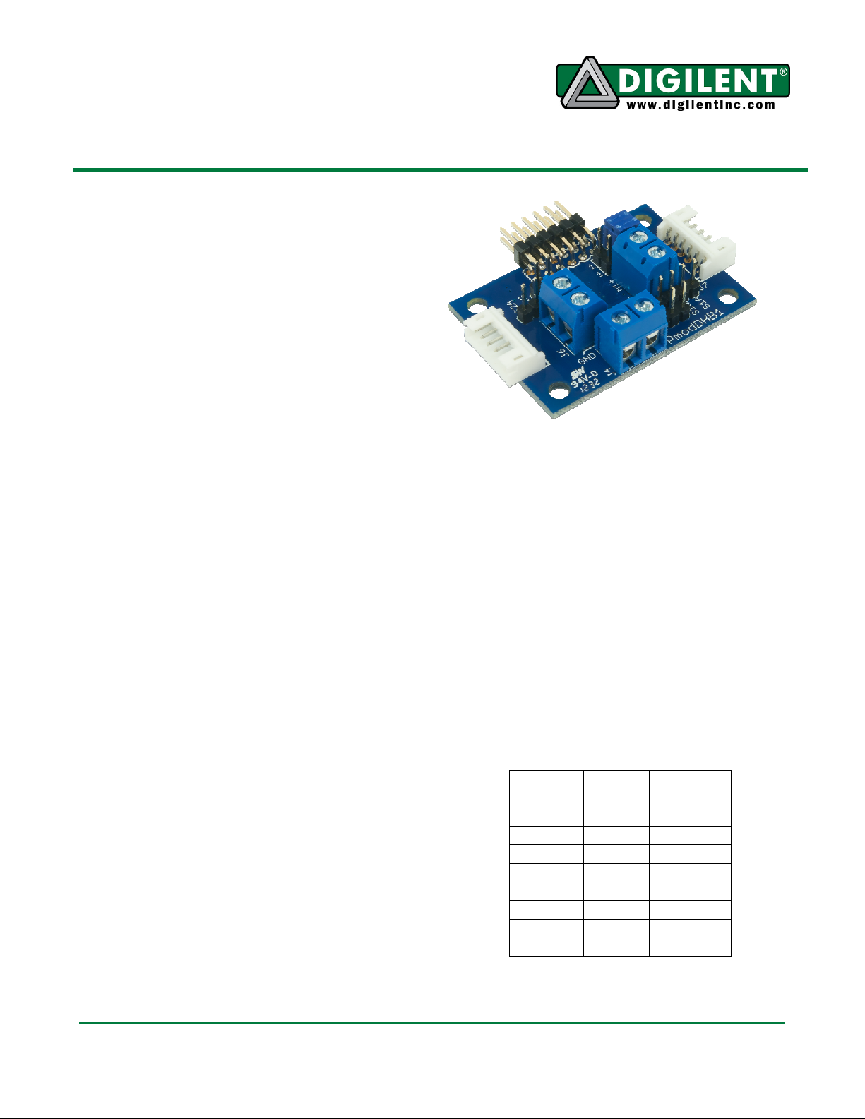
Overview
The PmodDHB1 uses the Texas Instruments
DRV8833 dual H-Bridge motor driver chip to
drive two DC motors or one stepper motor.
Features include:
• Motor voltage can be driven up to
11.8V, with a recommended 10.8V
maximum
• Two H-Bridge interfaces capable of
1.5A RMS (2A Peak)
• 2-channel quadrature encoder
channels for Hall-effect sensors
• Two JST 6-pin connectors for direct
connection to Digilent motor-gearboxes
• Logic input voltage range of 2.5V to 5V
Functional Description
For a detailed description of the Texas
Instruments DRV8833 please refer to the
device data sheet available at TI.com.
The DHB1 is controlled through the Pmod
connector J1. Logical levels on ENx and DIRx
determine the Motor Direction and speed of the
attached motors. The DHB1 uses a
demultiplexer and pull-down resistors on the
inputs to the DRV8833 H-Bridge pins to ensure
that the H-Bridge works in fast decay mode.
The intended operation of the DHB1 uses the
enable pin as the PWM input and the direction
pin as a logic level selector to set the direction
of the motor rotation. Table 1 lists the motor
responses that result from various input
combinations.
The DRV8833 chip provides overcurrent
protection on the motor drive circuits. Each
internal drive FET is independently monitored
for an overcurrent condition and will be shut
down internally to protect the chip. When an
1300 NE Henley Court, Suite 3
Pullman, WA 99163
(509) 334 6306 Voice | (509) 334 6300 Fax
overcurrent condition is sensed the chip will
shut down the FET with the fault and then set
the NFAULT pin low signaling a fault condition
on the chip. The remaining FETs will continue
to operate as normal. When the fault condition
is over, the chip will self-reset and return the
NFAULT logic level to logic high. (See Table 2
for connector descriptions.)
There are two Schmitt trigger buffered inputs
on connectors J2, J3, J7 and J8 that bring
motor speed feedback signals to the controlling
system board. The Digilent motor and gearbox
have hall-effect sensors arranged in a
quadrature encoder format. These buffers
have 5V tolerant inputs, when operated at
3.3V.
0 0 Stop
0 1/PWM Forward
1 0 Stop
1 1/PWM Reverse
0 0 Stop
0 1/PWM Forward
1 0 Stop
1 1/PWM Reverse
Table 1: Motor Control
Doc: 502-259 page 1 of 3
Copyright Digilent, Inc. All rights reserved. Other product and company names mentioned may be trademarks of their respective owners.
Page 2

PmodDHB1™ Reference Manual
Jumper
Setting
Description
Connector J1
– H-Bridge Interf
aces
Pin Signal
Description
Connector J2
- M1 JST 6
-
Pin Motor Connector
Connector J3
- M1 JST 6
-
Pin Motor Connector
Connector J4
- VM
Connector J5
- M1 Power
Connector J6
- M2 Power
Connector J7
- M1 Feedback
Connector J8
- M2 Feedback
Connector J9
- Fault
Connector J10
- Sleep
The quadrature encoder signals are a pair of
square waves whose frequency is proportional
to motor rotation speed and with the pulses 90°
out of phase. You can determine the motor
speed with the frequency and motor rotation
direction by the phase relationship between the
1 EN1 Motor 1 Enable
2 DIR1 Motor 1 Direction
3 S1A Motor 1 Sensor A Feedback
4 S1B Motor 1 Sensor B Feedback
5 GND Power Supply Ground
6 VCC Power Supply (3.3V)
7 EN2 Motor 2 Enable
8 DIR2 Motor 2 Direction
9 S2A Motor 2 Sensor A Feedback
10 S2B Motor 2 Sensor B Feedback
11 GND Power Supply Ground
12 VCC Power Supply (3.3V)
1 VM Motor Power
2 GND Power Supply Ground
1 M1+ Motor 1 Positive Supply
2 M1- Motor 1 Negative Supply
1 M2+ Motor 2 Positive Supply
2 M2- Motor 2 Negative Supply
1 SA1-IN Sensor A From Motor 1
2 SB1-IN Sensor B From Motor 1
3 GND Power Supply Ground
4 VCC Power Supply (3.3V)
1 SA2-IN Sensor A From Motor 2
2 SB2-IN Sensor B From Motor 2
3 GND Power Supply Ground
4 VCC Power Supply (3.3V)
1 NFAULT Overcurrent Condition
2 GND Power Supply Ground
1 NSLEEP Puts device into sleep state
2 GND Power Supply Ground
Table 2: Connector Descriptions
®
two signals.
www.digilentinc.com
Jumper Settings
Jumpers JP1 and JP2 allow both h-bridge
outputs to be run from the same enable and
direction pins. This allows the two bridge
outputs to be operated in parallel to drive a
single motor with twice the current. Refer to
Table 3 for available settings.
JP1
JP2
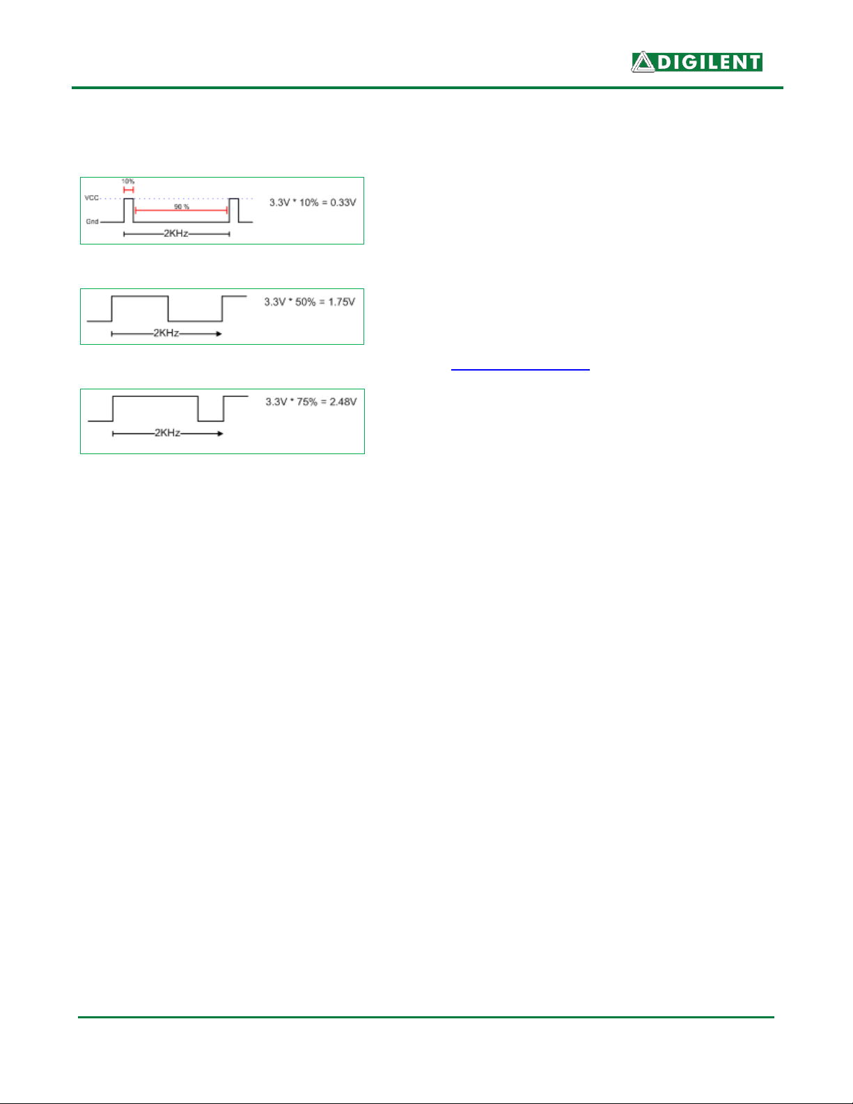
Pulse Width Modulation and Motor
Speed Control
Operators can control motor speed by varying
the input voltage to a circuit. However, you
can only apply a logic high or logic low signal
to the motor in a digital circuit. There are only
two ways to control a dc motor digitally. Either
use a variable resistance circuit to control the
motor voltage, or pulse the power to the motor.
Since variable resistance circuitry is expensive,
complicated, and energy inefficient because of
heat loss, Digilent recommends controlling
motor speed through pulse width modulation
(PWM).
Pulse width modulation is a digital method of
transmitting an analog signal. Even though
PWM is not a clean source of DC output
voltage, it controls motors well.
Figures 1 through 3 illustrate a PWM system
with an input frequency of 2KHz. You control
the motor speed by adjusting the time each
wave remains at peak output power. Figure 1
demonstrates a 10% “duty cycle,” where the
signal is logic high for only 1/10 of a
wavelength. This 10% positive peak is equal to
10% of the total 3.3V input, or 0.33V. (See
1 Motor 2 Uses EN1
3 Motor 2 Uses EN2
1 Motor 2 Uses DIR1
3 Motor 2 Uses DIR2
Table 3: Set Jumper Description
www.digilentinc.com Copyright Digilent, Inc. page 2 of 3
Page 3
PmodDHB1™ Reference Manual
Figure 1.) Figures 2 and 3 represent duty
cycles of 50% and 75%.
Figure 1. 10% Duty Cycle
Figure 2. 50% Duty Cycle
Figure 3. 75% Duty Cycle
An H-bridge is a voltage amplification and
direction control circuit. Customers should use
the H-bridge to format the signal to the
appropriate motor voltage and polarity to spin
the motor.
The changing magnetic forces that occur as
you intermittently apply voltage drive the
motor. Even when the voltage stops,
momentum causes the motor to continue
spinning. At a high enough frequency, this
process of powering and coasting enables the
motor to achieve a smooth rotation that can
easily be controlled through digital logic.
PWM has two important effects on DC motors.
PWM overcomes inertial resistance more
easily at startup because short bursts of
maximum voltage achieve a greater degree of
torque than the equivalent DC voltage. PWM
also generates a higher level of heat inside the
motor. If customers use a pulsed motor for an
extended time, they will need heat dissipation
systems to prevent damage to the motor.
Because of these effects, it is best to use PWM
in high-torque infrequent-use applications such
as airplane flap servos and robotics.
www.digilentinc.com
PWM circuits can also create radio frequency
interference (RFI) that operators can minimize
by locating motors near the controller and by
using short wires. You may also need to filter
line noise created by continually powering up
the motor to prevent interference with the rest
of the circuits. You can place small ceramic
capacitors directly across the motor terminals
and between the motor terminals and the
motor case to filter the RFI emissions from the
motor.
Note: For more information on the Pmod
DHB1 see the product page at
www.digilentinc.com.
®
www.digilentinc.com Copyright Digilent, Inc. page 3 of 3
 Loading...