

Page 1
Anvyl™ Reference Manual
Revision: May 23, 2013
Note: This document applies to REV B of the board
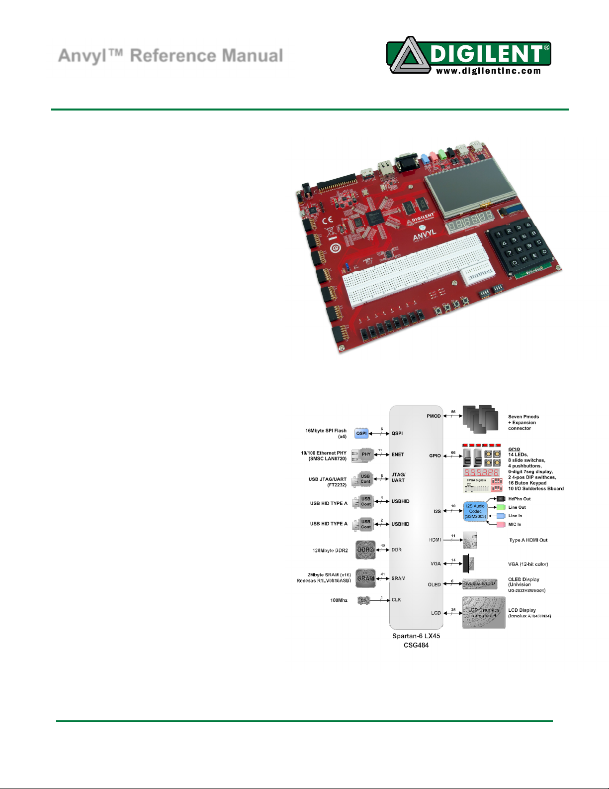
Overview
The Anvyl FPGA development platform is
a complete, ready-to-use digital circuit
development platform based on a speed
grade -3 Xilinx Spartan-6 LX45 FPGA.
The large FPGA, along with the 100-mbps
Ethernet, HDMI Video, 128MB DDR2
memory, 4.3” LED backlit LCD
touchscreen, 128x32 pixel OLED display,
630 tie-point breadboard, multiple USB
HID controllers, and I2S audio codec,
makes the Anvyl an ideal platform for an
FPGA learning station capable of
supporting embedded processor designs
based on Xilinx’s MicroBlaze. The Anvyl is
compatible with all Xilinx CAD tools,
including ChipScope, EDK, and the free
ISE WebPack™, so designs can be
completed at no extra cost. The board
dimensions are 27.5cm x 21cm.
The Spartan-6 LX45 is optimized for high
performance logic and offers:
• 6,822 slices, each containing four
input LUTs and eight flip-flops
• 2.1Mbits of fast block RAM
• four clock tiles (eight DCMs & four
PLLs)
• 58 DSP slices
• 500MHz+ clock speeds
1300 NE Henley Court, Suite 3
Pullman, WA 99163
(509) 334 6306 Voice | (509) 334 6300 Fax
A comprehensive collection of board
support IP and reference designs, and a
large collection of add-on boards are
available on the Digilent website. See the
Anvyl page at www.digilentinc.com for
more information.
Doc: 502-258 page 1 of 16
Copyright Digilent, Inc. All rights reserved. Other product and company names mentioned may be trademarks of their respective owners.
Page 2

Anvyl Reference Manual
Features include:
• Spartan6-LX45 FPGA:XC6SLX45-CSG484-3
• 128MB DDR2 SDRAM
• 2MB SRAM
• 16MB QSPI FLASH for configuration and data storage
• 10/100 Ethernet PHY
• HDMI Video Output
• 12-bit VGA port
• 4.3” wide-format vivid color LED backlit LCD screen
• 128x32 pixel 0.9’’ WiseChip/Univision UG-23832HSWEG04 OLED graphic display panel
• three two-digit Seven Segment LED displays
• I2S Audio codec with line-in, line-out, mic, and headphone
• 100MHz Crystal Oscillator
• on-board USB2 ports for programming and USB-HID devices (for mouse/keyboard)
• Digilent USB-JTAG circuitry with USB-UART functionality
• keypad with 16 labeled keys (0-F)
• GPIO: 14 LEDs (10 red, 2 yellow, 2 green), 8 slide switches, 8 DIP switches in 2 groups and 4
push buttons
• breadboard with 10 Digital I/O’s
• 32 I/O’s routed to 40-pin expansion connector (I/O’s are shared with Pmod connectors)
• seven 12-pin Pmod connectors with 56 I/O’s total
• ships with a 20W power supply and USB cable
FPGA Configuration
After being turned on, the FPGA on the Anvyl board must be configured (or programmed) before it
can perform any functions. The FPGA can be configured in three ways: a PC can use the Digilent
USB-JTAG circuitry (port J12, labeled “PROG”) to program the FPGA any time power is on, a
configuration file stored in the onboard SPI Flash ROM can be automatically transferred to the FPGA
at power-on, or a programming file can be transferred from a USB memory stick to the USB HID port
labeled “Host” (J14).
An on-board mode jumper (JP2) selects between JTAG/USB and ROM programming modes. If JP2 is
not loaded, the FPGA will automatically configure itself from the ROM. If JP2 is loaded, the FPGA will
remain idle after power-on until configured from the JTAG or Serial programming port (USB memory
stick).
Both Digilent and Xilinx freely distribute software that can be used to program the FPGA and the SPI
ROM. Programming files are stored within the FPGA in SRAM-based memory cells. This data defines
the FPGA’s logic functions and circuit connections, and it remains valid until it is erased by removing
power, asserting the PROG_B input, or until it is overwritten by a new configuration file.
FPGA configuration files transferred via the JTAG port and from a USB stick use the .bit file type, and
SPI programming files use the .mcs file type. Xilinx’s ISE WebPack and EDK software can create .bit
www.digilentinc.com page 2 of 16
Copyright Digilent, Inc. All rights reserved. Other product and company names mentioned may be trademarks of their respective owners.
Page 3

Anvyl Reference Manual
files from VHDL, Verilog, or schematic-based source files (EDK is used for MicroBlaze™ embedded
processor based designs). Once a .bit file has been created, the Anvyl’s FPGA can be programmed
with it over the USB-JTAG circuitry (port J12) using either Digilent’s Adept software or Xilinx’s
iMPACT software. To generate a .mcs file from a .bit file, use the PROM File Generator tool within
Xilinx’s iMPACT software. The .mcs file can then be programmed to the SPI Flash using iMPACT.
The FPGA can also be programmed from a FAT formatted memory stick attached to the USB-HID
HOST port (J14) if the stick contains a single .bit configuration file in the root directory, JP2 is loaded,
and board power is cycled. The FPGA will automatically reject any .bit files that are not built for the
proper FPGA.
Power Supplies
The Anvyl board requires an external 5V, 4A or greater power source with a center positive, 2.1mm
internal diameter coax plug (a suitable supply is provided as part of the Anvyl kit). Voltage regulator
circuits from Analog Devices create the required 3.3V, 1.8V and 1.2V supplies from the main 5V
supply. A power-good LED (LD19), driven by the wired OR of all the power-good outputs on the
supplies, indicates that all supplies are operating normally. The following devices are present on each
rail:
• 5V : USB-HID connectors, TFT touchscreen controller, HDMI, and expansion connector
• 3.3V : SRAM, Ethernet PHY I/O, USB-HID controllers, FPGA I/O, oscillators, SPI Flash, Audio
codec, TFT display, OLED display, GPIO, Pmods, and expansion connector
• 1.8V : DDR2, USB-JTAG/USB-UART controller, FPGA I/O, and GPIO
• 1.2V : FPGA core and Ethernet PHY core
Adept System
Adept has a simplified configuration interface. To program the Anvyl board using Adept, first set up
the board and initialize the software:
• plug in and attach the power supply
• plug in the USB cable to the PC and to the USB PROG port on the board
• start the Adept software
• turn ON Anvyl’s power switch
• wait for the FPGA to be recognized
Use the browse function to associate the desired .bit file with the FPGA, and click on the Program
button. The configuration file will be sent to the FPGA, and a dialog box will indicate whether
programming was successful. The configuration “done” LED will light up after the FPGA has been
successfully configured. Before starting the programming sequence, Adept ensures that any selected
configuration files contain the correct FPGA ID code – this prevents incorrect .bit files from being sent
to the FPGA. In addition to the navigation bar and browse and program buttons, the configuration
interface provides an Initialize Chain button, console window, and status bar. The Initialize Chain
button is useful if USB communications with the board have been interrupted. The console window
displays current status, and the status bar shows real-time progress when downloading a
configuration file.
www.digilentinc.com page 3 of 16
Copyright Digilent, Inc. All rights reserved. Other product and company names mentioned may be trademarks of their respective owners.
Page 4

Anvyl Reference Manual
DDR2 Memory
A single 1Gbit DDR2 memory chip is driven from the memory controller block in the Spartan-6 FGPA.
The DDR2 device, a MT47H64M16HR-25E or equivalent, provides a 16-bit bus and 64M locations.
The Anvyl board has been tested for DDR2 operation at up to an 800MHz data rate. The DDR2
interface follows the pin-out and routing guidelines specified in the Xilinx Memory Interface Generator
(MIG) User Guide. The interface supports SSTL18 signaling, and all address, data, clocks, and
control signals are delay-matched and impedance-controlled. Two well-matched DDR2 clock signal
pairs are provided so the DDR can be driven with low-skew clocks from the FPGA.
Flash Memory
The Anvyl board uses a 128Mbit Numonyx N25Q128
Serial flash memory device (organized as 16Mbit by 8) for
non-volatile storage of FPGA configuration files. The SPI
Flash can be programmed with a .mcs file using the
iMPACT software. An FPGA configuration file requires
less than 12Mbits, leaving 116Mbits available for user
data. Data can be transferred to and from a PC to/from
the flash device by user applications, or by facilities built
into the iMPACT PROM file generation software. User
designs programmed into the FPGA can also transfer
data to and from the flash.
A board test/demonstration program is loaded into the SPI Flash during manufacturing.
Ethernet PHY
The Anvyl board includes an SMSC 10/100 mbps PHY (LAN8720A-CP-TR) paired with a Halo
HFJ11-2450E RJ-45 connector. The PHY is connected to the FPGA using a RMII configuration. It is
configured to boot into “All Capable, with Auto Negotiation Enabled” mode on power-on. The data
sheet for the SMSC PHY is available from the SMSC website.
HDMI Output
The Anvyl board contains one unbuffered HDMI output port. The unbuffered port uses an HDMI type
A connector. Since the HDMI and DVI systems use the same TMDS signaling standard, a simple
adaptor (available at most electronics stores) can be used to drive a DVI connector from the HDMI
output port. The HDMI connector does not include VGA signals, so analog displays cannot be driven.
The 19-pin HDMI connectors include four differential data channels, five GND connections, a one-wire
Consumer Electronics Control (CEC) bus, a two-wire Display Data Channel (DDC) bus that is
essentially an I2C bus, a Hot Plug Detect (HPD) signal, a 5V signal capable of delivering up to 50mA,
and one reserved (RES) pin. Of these, the differential data channels, I2C bus, and CEC are connected
to the FPGA.
www.digilentinc.com page 4 of 16
Copyright Digilent, Inc. All rights reserved. Other product and company names mentioned may be trademarks of their respective owners.
Page 5
Anvyl Reference Manual
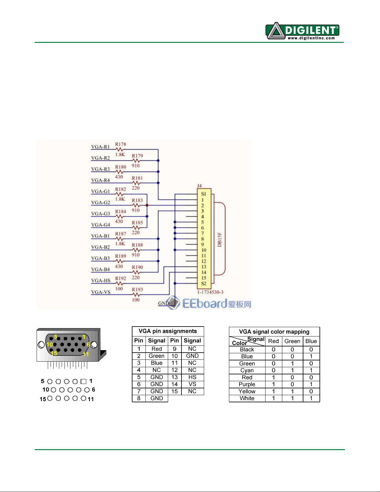
VGA
The Anvyl provides a 12bit VGA interface which allows up to 4096 colors displayed on a standard
VGA Monitor. The five standard VGA signals Red, Green, Blue, Horizontal Sync (HS), and Vertical
Sync (VS) are routed directly from the FPGA to the VGA connector. There are four signals routed
from the FPGA for each of the standard VGA color signals resulting in a video system that can
produce 4,096 colors. Each of these signals has a series resistor that when combined in the circuit,
form a divider with the 75-ohm termination resistance of the VGA display. These simple circuits
ensure that the video signals cannot exceed the VGA-specified maximum voltage, and result in color
signals that are either fully on (.7V), fully off (0V) or somewhere in between.
Fig. 2. VGA interface.
Fig. 3. HD DB-15 connector, PCB hole pattern, pin assignments, and color-signal mapping.
www.digilentinc.com page 5 of 16
Copyright Digilent, Inc. All rights reserved. Other product and company names mentioned may be trademarks of their respective owners.
Page 6

Anvyl Reference Manual
CRT-based VGA displays use amplitude-modulated moving electron beams (or cathode rays) to
display information on a phosphor-coated screen. LCD displays use an array of switches that can
impose a voltage across a small amount of liquid crystal, thereby changing light permittivity through
the crystal on a pixel-by-pixel basis. Although the following description is limited to CRT displays, LCD
displays have evolved to use the same signal timings as CRT displays (so the “signals” discussion
below pertains to both CRTs and LCDs). Color CRT displays use three electron beams (one for red,
one for blue, and one for green) to energize the phosphor that coats the inner side of the display end
of a cathode ray tube (see Fig. 1). Electron beams emanate from “electron guns”, which are finelypointed heated cathodes placed in close proximity to a positively charged annular plate called a “grid”.
The electrostatic force imposed by the grid pulls rays of energized electrons from the cathodes, and
those rays are fed by the current that flows into the cathodes. These particle rays are initially
accelerated towards the grid, but they soon fall under the influence of the much larger electrostatic
force that results from the entire phosphor-coated display surface of the CRT being charged to 20kV
(or more). The rays are focused to a fine beam as they pass through the center of the grids, and then
they accelerate to impact on the phosphor-coated display surface. The phosphor surface glows
brightly at the impact point, and it continues to glow for several hundred microseconds after the beam
is removed. The larger the current fed into the cathode, the brighter the phosphor will glow.
Fig. 4. Cathode ray tube display system.
Between the grid and the display surface, the electron beam passes through the neck of the CRT
where two coils of wire produce orthogonal electromagnetic fields. Because cathode rays are
composed of charged particles (electrons), they can be deflected by these magnetic fields. Current
waveforms are passed through the coils to produce magnetic fields that interact with the cathode rays
and cause them to transverse the display surface in a “raster” pattern, horizontally from left to right
and vertically from top to bottom. As the cathode ray moves over the surface of the display, the
current sent to the electron guns can be increased or decreased to change the brightness of the
display at the cathode ray impact point.
VGA System Timing
www.digilentinc.com page 6 of 16
Copyright Digilent, Inc. All rights reserved. Other product and company names mentioned may be trademarks of their respective owners.
Page 7

Anvyl Reference Manual
VGA signal timings are specified, published, copyrighted and sold by the VESA organization
(www.vesa.org). The following VGA system timing information is provided as an example of how a
VGA monitor might be driven with a resolution of 640x480. For more precise information, or for
information on other VGA frequencies, refer to documentation available at the VESA website.
Information is only displayed when the beam is moving “forward” (left to right and top to bottom), and
not during the time the beam is reset back to the left or top edge of the display. Much of the potential
display time is therefore lost in “blanking” periods when the beam is reset and stabilized to begin a
new horizontal or vertical display pass. The size of the beams, the frequency at which the beam can
be traced across the display, and the frequency at which the electron beam can be modulated
determine the display resolution. Modern VGA displays can accommodate different resolutions, and a
VGA controller circuit dictates the resolution by producing timing signals to control the raster patterns.
The controller must produce synchronizing pulses at 3.3V (or 5V) to set the frequency at which
current flows through the deflection coils, and it must ensure that video data is applied to the electron
guns at the correct time. Raster video displays define a number of “rows” that corresponds to the
number of horizontal passes the cathode makes over the display area, and a number of “columns”
that corresponds to an area on each row that is assigned to one “picture element” or pixel. Typical
displays use from 240 to 1200 rows and from 320 to 1600 columns. The overall size of a display and
the number of rows and columns determines the size of each pixel.
Video data typically comes from a video refresh memory, with one or more bytes assigned to each
pixel location (the Anvyl uses four bits per pixel). The controller must index into video memory as the
beams move across the display, and retrieve and apply video data to the display at precisely the time
the electron beam is moving across a given pixel.
pixel 0,0
pixel 0,639
640 pixels are displayed each
time the beam travels across
the screen
VGA display
Current
through
horizontal
defletion
coil
time
HS
surface
pixel 479,0 pixel 479,639
Stable current ramp - information
displayed during this time
Total horizontal time
Horizontal display time
Horizontal sync signal
sets retrace frequency
retrace
time
"back porch""front porch"
Retrace - no
information
displayed
during this
time
Fig. 5. VGA horizontal synchronization.
www.digilentinc.com page 7 of 16
Copyright Digilent, Inc. All rights reserved. Other product and company names mentioned may be trademarks of their respective owners.
Page 8

Anvyl Reference Manual
A VGA controller circuit must generate the HS and VS timings signals and coordinate the delivery of
video data based on the pixel clock. The pixel clock defines the time available to display one pixel of
information. The VS signal defines the “refresh” frequency of the display, or the frequency at which all
information on the display is redrawn. The minimum refresh frequency is a function of the display’s
phosphor and electron beam intensity, with practical refresh frequencies falling in the 50Hz to 120Hz
range. The number of lines to be displayed at a given refresh frequency defines the horizontal
“retrace” frequency. For a 640-pixel by 480-row display using a 25MHz pixel clock and 60 +/-1Hz
refresh, the signal timings shown in the table below can be derived. Timings for sync pulse width and
front and back porch intervals (porch intervals are the pre- and post-sync pulse times during which
information cannot be displayed) are based on observations taken from actual VGA displays.
A VGA controller circuit decodes the output of a horizontal-sync counter driven by the pixel clock to
generate HS signal timings. This counter can be used to locate any pixel location on a given row.
Likewise, the output of a vertical-sync counter that increments with each HS pulse can be used to
generate VS signal timings, and this counter can be used to locate any given row. These two
continually running counters can be used to form an address into video RAM. No time relationship
between the onset of the HS pulse and the onset of the VS pulse is specified, so the designer can
arrange the counters to easily form video RAM addresses, or to minimize decoding logic for sync
pulse generation.
Symbol Parameter
T
Sync pulse time
S
T
Display time
disp
T
VS pulse width
pw
T
VS front porch
fp
T
VS back porch
bp
Vertical Sync
Time Clocks Lines
16.7ms
15.36ms
320 us
928 us
64 us
416,800
384,000
1,600
8,000
23,200
Horizontal Sync
Time
521
480
25.6 us
2
3.84 us
10
640 ns
29
1.92 us
32 us
Clocks
800
640
96
16
48
T
S
T
disp
T
pw
T
fp
T
bp
Fig. 6. VGA sync signal timings.
Fig. 7. VGA display controller block diagram.
Audio (I2S)
The Anvyl board includes an Analog Devices audio codec SSM2603CPZ (IC5) with four 1/8” audio
jacks for line-out (J7), headphone-out (J6), line-in (J9), and microphone-in (J8).
www.digilentinc.com page 8 of 16
Copyright Digilent, Inc. All rights reserved. Other product and company names mentioned may be trademarks of their respective owners.
Page 9

Anvyl Reference Manual
Audio data sampling at up to 24 bits and 96KHz is supported, and the audio in (record) and audio out
(playback) sampling rates can be set independently. The microphone jack is mono, and all other jacks
are stereo. The headphone jack is driven by the audio codec's internal amplifier. The datasheet for the
SSM2603CPZ audio codec is available from the Analog Devices website.
Touchscreen TFT Display
A 4.3” wide-format vivid color LED backlit LCD screen is used on the Anvyl. The screen has a
480×272 native resolution display with a color depth of 24 bits per pixel. A four-wire resistive
touchscreen with antiglare coating covers the entire active display area. The LCD screen and the
touchscreen can be used independently. Touch readings are noisier when the LCD is on, but you can
filter the noise and still obtain a fast sample rate. If you require maximum precision and sample rates,
you should turn the LCD off during touchscreen sampling.
To display an image, the LCD needs to be continuously driven with properly-timed data. This data
consists of the lines and blanking periods that form video frames. Each frame consists of 272 active
lines and several vertical blanking lines. Each line consists of 480 active pixel periods and several
horizontal blanking periods.
For additional information on using the TFT Display, refer to the Vmod-TFT reference manual. The
Anvyl and the Vmod-TFT use the same display hardware and require the same control signals.
Reference designs that use the Anvyl touchscreen TFT display can be found on the Anvyl product
page.
OLED
An Inteltronic/Wisechip UG-2832HSWEG04 OLED Display is used on the Anvyl. This provides a
128x32 pixel, passive-matrix, monochrome display. The display size is 30mm x 11.5mm x 1.45mm.
An SPI interface is used to configure the display, as well as to send the bitmap data to the device. The
Anvyl OLED displays the last image drawn on the screen until it is powered down or a new image is
drawn to the display. Refreshing and updating is handled internally.
The Anvyl contains the same OLED circuit as the PmodOLED, with the exception that CS# is pulled
low, enabling the display by default. For additional information on driving the Anvyl OLED, refer to the
PmodOLED reference manual. Reference designs that use the Anvyl OLED display can be found on
the Anvyl product page.
USB-UART Bridge (Serial Port)
The Anvyl includes an FTDI FT2232HQ USBUART bridge to allow PC applications to
communicate with the board using standard
Windows COM port commands. Free USBCOM port drivers, available from
www.ftdichip.com under the "Virtual Com
Port" or VCP heading, convert USB packets to UART/serial port data. Serial port data is exchanged
with the FPGA using a two-wire serial port (TXD/RXD) and software flow control (XON/XOFF). After
the drivers are installed, I/O commands from the PC directed to the COM port will produce serial data
traffic on the T19 and T20 FPGA pins.
www.digilentinc.com page 9 of 16
Copyright Digilent, Inc. All rights reserved. Other product and company names mentioned may be trademarks of their respective owners.
Page 10

Anvyl Reference Manual
The FT2232HQ, attached to port J12, is also used as the controller for the Digilent USB-JTAG
circuitry, but these two functions behave entirely independent of one another. Programmers interested
in using the UART functionality of the FT2232 within their design do not need to worry about the JTAG
circuitry interfering with their data, and vice-versa.
USB HID Hosts
Two Microchip PIC24FJ128GB106
microcontrollers provide the Anvyl
with USB HID host capability.
Firmware in the microcontrollers
can drive a mouse or a keyboard
attached to the type A USB
connectors at J13 and J14 labeled
"HID" and “HOST”. Hubs are not
supported, so only a single mouse
or a single keyboard can be used
at each port.
The “HOST” PIC24 drives four
signals into the FPGA – two are dedicated as a keyboard/mouse port following the PS/2 protocol, and
two are connected to the FPGA’s two-wire serial programming port, so the FPGA can be programmed
from a file stored on a USB memory stick. To program the FPGA, attach a FAT formatted memory
stick containing a single .bit programming file in the root directory, load JP2, and cycle board power.
This will cause the PIC processor to program the FPGA, and any incorrect bit files will automatically
be rejected. Note the PIC24 reads the FPGA's mode, init, and done pins, and can drive the PROG pin
as a part of the programming sequence.
HID Controller
To access a USB host controller, EDK designs can use the standard PS/2 core (non-EDK designs
can use a simple state machine).
Fig. 10. PS/2 Timing Diagram
www.digilentinc.com page 10 of 16
Copyright Digilent, Inc. All rights reserved. Other product and company names mentioned may be trademarks of their respective owners.
Page 11

Anvyl Reference Manual
Mice and keyboards that use the PS/2 protocol1 use a two-wire serial bus (clock and data) to
communicate with a host device. Both use 11-bit words that include a start, stop, and odd parity bit,
but the data packets are organized differently, and the keyboard interface allows bi-directional data
transfers (so the host device can illuminate state LEDs on the keyboard). Bus timings are shown in
the figure. The clock and data signals are only driven when data transfers occur, and otherwise they
are held in the idle state at logic ‘1’. The timings define signal requirements for mouse-to-host
communications and bi-directional keyboard communications. A PS/2 interface circuit can be
implemented in the FPGA to create a keyboard or mouse interface.
Keyboard
The keyboard uses open-collector drivers so the keyboard, or an attached host device, can drive the
two-wire bus (if the host device will not send data to the keyboard, then the host can use input-only
ports).
PS/2-style keyboards use scan codes to communicate key press data. Each key is assigned a code
that is sent whenever the key is pressed. If the key is held down, the scan code will be sent
repeatedly about once every 100ms. When a key is released, an F0 (binary “11110000”) key-up code
is sent, followed by the scan code of the released key. If a key can be shifted to produce a new
character (like a capital letter), then a shift character is sent in addition to the scan code, and the host
must determine which ASCII character to use. Some keys, called extended keys, send an E0 (binary
“11100000”) ahead of the scan code (and they may send more than one scan code). When an
extended key is released, an E0 F0 key-up code is sent, followed by the scan code. Scan codes for
most keys are shown in the figure. A host device can also send data to the keyboard. Below is a short
list of some common commands a host might send.
ED Set Num Lock, Caps Lock, and Scroll Lock LEDs. Keyboard returns FA after receiving ED,
then host sends a byte to set LED status: bit 0 sets Scroll Lock, bit 1 sets Num Lock, and bit 2
sets Caps lock. Bits 3 to 7 are ignored.
EE Echo (test). Keyboard returns EE after receiving EE.
F3 Set scan code repeat rate. Keyboard returns F3 on receiving FA, then host sends second byte
to set the repeat rate.
FE Resend. FE directs keyboard to re-send most recent scan code.
FF Reset. Resets the keyboard.
The keyboard can send data to the host only when both the data and clock lines are high (or idle).
Since the host is the bus master, the keyboard must check to see whether the host is sending data
before driving the bus. To facilitate this, the clock line is used as a “clear to send” signal. If the host
pulls the clock line low, the keyboard must not send any data until the clock is released. The keyboard
sends data to the host in 11-bit words that contain a ‘0’ start bit, followed by 8-bits of scan code (LSB
first), followed by an odd parity bit and terminated with a ‘1’ stop bit. The keyboard generates 11 clock
transitions (at 20 to 30KHz) when the data is sent, and data is valid on the falling edge of the clock.
Not all keyboard manufacturers strictly adhere to the PS/2 specifications; some keyboards may not
produce the proper signaling voltages or use the standard communication protocols. Compatibility
with the USB host may vary between different keyboards. 1
www.digilentinc.com page 11 of 16
Copyright Digilent, Inc. All rights reserved. Other product and company names mentioned may be trademarks of their respective owners.
Page 12

Anvyl Reference Manual
Scan codes for most PS/2 keys are shown in the figure below.
Fig. 11. PS/2 keyboard scan codes.
Mouse
The mouse outputs a clock and data signal when it is moved, otherwise, these signals remain at logic
‘1’. Each time the mouse is moved, three 11-bit words are sent from the mouse to the host device.
Each of the 11-bit words contains a ‘0’ start bit, followed by 8 bits of data (LSB first), followed by an
odd parity bit, and terminated with a ‘1’ stop bit. Thus, each data transmission contains 33 bits, where
bits 0, 11, and 22 are ‘0’ start bits, and bits 11, 21, and 33 are ‘1’ stop bits. The three 8-bit data fields
contain movement data as shown in the figure above. Data is valid at the falling edge of the clock, and
the clock period is 20 to 30KHz.
The mouse assumes a relative coordinate system wherein moving the mouse to the right generates a
positive number in the X field, and moving to the left generates a negative number. Likewise, moving
the mouse up generates a positive number in the Y field, and moving down represents a negative
number (the XS and YS bits in the status byte are the sign bits – a ‘1’ indicates a negative number).
The magnitude of the X and Y numbers represent the rate of mouse movement – the larger the
number, the faster the mouse is moving (the XV and YV bits in the status byte are movement overflow
indicators – a ‘1’ means overflow has occurred). If the mouse moves continuously, the 33-bit
transmissions are repeated every 50ms or so. The L and R fields in the status byte indicate Left and
Right button presses (a ‘1’ indicates the button is being pressed).
Fig. 12. Mouse navigation bytes.
Keypad
The Anvyl keypad has 16 labeled keys (0-F). It is set up as a matrix in which each row of buttons from
left to right are tied to a row pin, and each column from top to bottom is tied to a column pin. This
www.digilentinc.com page 12 of 16
Copyright Digilent, Inc. All rights reserved. Other product and company names mentioned may be trademarks of their respective owners.
Page 13

Anvyl Reference Manual
Keypad
Pinout
gives the user four row pins and four column pins to address a button push. When a button is
pressed, the pins corresponding to that button’s row and column are connected.
To read a button’s state, the column pin in which the button resides must be driven low while the other
three column pins are driven high. This enables all of the buttons in that column. When a button in
that column is pushed, the corresponding row pin will read logic low.
The state of all 16 buttons can be determined in a four-step process by enabling each of the four
columns one at a time. This can be accomplished by rotating an “1110” pattern through the column
pins. During each step, the logic levels of the row pins correspond to the state of the buttons in that
column.
To allow simultaneous button presses in the same row, instead configure the column pins as bidirectional with internal pull-up resistors and keep the columns not currently being read at high
impedance.
ROW1:
ROW2:
ROW3:
ROW4:
COL1:
COL2:
COL3:
COL4:
E4
F3
G8
G7
H8
J7
K8
K7
Fig. 13. Keypad schematic
Oscillators/Clocks
The Anvyl board includes a single 100MHz Crystal oscillator connected to pin D11 (D11 is a GCLK
input in bank 0). The input clock can drive any or all of the four clock management tiles in the Spartan-
6. Each tile includes two Digital Clock Managers (DCMs) and one Phase-Locked Loop (PLLs).DCMs
provide the four phases of the input frequency (0º, 90º, 180º, and 270º), a divided clock that can be
the input clock divided by any integer from 2 to 16 or 1.5, 2.5, 3.5... 7.5, and two antiphase clock
outputs that can be multiplied by any integer from 2 to 32 and simultaneously divided by any integer
from 1 to 32.
PLLs use Voltage Controlled Oscillators (VCOs) that can be programmed to generate frequencies in
the 400MHz to 1080MHz range by setting three sets of programmable dividers during FPGA
www.digilentinc.com page 13 of 16
Copyright Digilent, Inc. All rights reserved. Other product and company names mentioned may be trademarks of their respective owners.
Page 14

Anvyl Reference Manual
Push
Slide
DIP
V19
configuration. VCO outputs have eight equally-spaced outputs (0º, 45º, 90º, 135º, 180º, 225º, 270º,
and 315º) that can be divided by any integer between 1 and 128.
Basic I/O
The Anvyl board includes fourteen LEDs (ten red, two yellow, and two green), eight slide switches,
eight DIP switches in two groups, four push buttons, three two-digit seven-segment displays, and a
630 tie-point breadboard with ten digital I/O’s. The push buttons, slide switches and DIP switches are
connected to the FPGA via series resistors to prevent damage from inadvertent short circuits (a short
circuit could occur if an FPGA pin assigned to a pushbutton or slide switch was inadvertently defined
as an output). The pushbuttons are "momentary" switches that normally generate a low output when
they are at rest, and a high output only when they are pressed. Slide switches and DIP switches
generate constant high or low inputs depending on their position. The ten digital breadboard I/O’s
(BB1 – BB10) are connected directly to the FPGA so that they can easily be incorporated into custom
circuits.
Buttons
BTN0: E6 SW0:V5 DIP8-1: G6 LD0:W3 LD9:R7 BB1: AB20 BB9:R19
BTN1: D5 SW1:U4 DIP8-2: G4 LD1:Y4 LD10:U6 BB2: P17 BB10:
BTN2: A3 SW2:V3 DIP8-3: F5 LD2:Y1 LD11:T8 BB3: P18
BTN3: AB9 SW 3:P4 DIP8-4: E5 LD3:Y3 LD12:T7 BB4: Y19
SW4:R4 DIP9-1: F8 LD4:AB4 LD13:W4 BB5: Y20
SW5:P6 DIP9-2: F7 LD5:W1 LD14:U8 BB6: R15
SW6:P5 DIP9-3: C4 LD6:AB3 BB7: R16
SW7:P8 DIP9-4: D3 LD7:AA4 BB8: R17
Switches
Switches LEDs Breadboard
Table 1. Basic I/O pinout.
Seven Segment Display
The Anvyl board contains three 2-digit common cathode seven-segment LED displays. Each of the
two digits is composed of seven segments arranged in a “figure eight” pattern, with an LED embedded
in each segment. Segment LEDs can be individually illuminated, so any one of 128 patterns can be
displayed on a digit by illuminating certain LED segments and leaving the others dark. Of these 128
possible patterns, the ten corresponding to the decimal digits are the most useful.
The common cathode signals are available as six “digit enable” input signals to the three 2-digit
displays. The anodes of similar segments on all six digits are connected into seven circuit nodes
labeled AA through AG (so, for example, the six “D” anodes from the six digits are grouped together
into a single circuit node called “AD”). These seven anode signals are available as inputs to the 2-digit
displays. This signal connection scheme creates a multiplexed display, where the anode signals are
common to all digits but they can only illuminate the segments of the digit whose corresponding
cathode signal is asserted.
A scanning display controller circuit can be used to show a two-digit number on each display. This
circuit drives the cathode signals and corresponding anode patterns of each digit in a repeating,
continuous succession, at an update rate that is faster than the human eye response. Each digit is
illuminated just one-sixth of the time, but because the eye cannot perceive the darkening of a digit
before it is illuminated again, the digit appears continuously illuminated. If the update (or “refresh”)
rate is slowed to a given point (around 45 hertz), then most people will begin to see the display flicker.
www.digilentinc.com page 14 of 16
Copyright Digilent, Inc. All rights reserved. Other product and company names mentioned may be trademarks of their respective owners.
Page 15

Anvyl Reference Manual
In order for each of the six digits to appear bright and continuously illuminated, each digit should be
driven once every 1 to 16ms (for a refresh frequency of 1KHz to 60Hz). For example, in a 60Hz
refresh scheme, the entire display would be refreshed once every 16ms, and each digit would be
illuminated for 1/6 of the refresh cycle, or 2.67ms. The controller must assure that the correct anode
pattern is present when the corresponding cathode signal is driven. To illustrate the process, if Cat1 is
asserted while AB and AC are asserted, then a “1” will be displayed in digit position 1. Then, if Cat2 is
asserted while AA, AB and AC are asserted, then a “7” will be displayed in digit position 2. If Cat1 and
AB, AC are driven for 8ms, and then Cat2 and AA, AB, AC are driven for 8ms in an endless
succession, the display will show “17”. An example timing diagram for a two-digit controller is shown
below.
Individual anodes
An un-illuminated seven-segment display, and nine
illumination patterns corresponding to decimal digits
Two-digit Seven
Segment Display
F
E
D
Common cathode
A
G
B
C
Fig. 14. Seven-segment displays.
Expansion Connectors
The Anvyl board has a 2x20 pin connector and seven 12-pin Pmod connectors. Pmod connectors are
2x6 right-angle, 100-mil female connectors that work with standard 2x6 pin headers available from a
variety of catalog distributors. Each 12-pin Pmod connector provides two 3.3V VCC signals (pins 6
and 12), two Ground signals (pins 5 and 11), and eight logic signals. VCC and Ground pins can
deliver up to 1A of current. Pmod data signals are not matched pairs, and they are routed using bestavailable tracks without impedance control or delay matching. Digilent produces a large collection of
Pmod accessory boards that can attach to the Pmod connectors. We have a set of recommended
Pmods for the Anvyl called the “Anvyl Pmod Pack”.
www.digilentinc.com page 15 of 16
Copyright Digilent, Inc. All rights reserved. Other product and company names mentioned may be trademarks of their respective owners.
Page 16

Anvyl Reference Manual
Pmod JA
Pmod JB
Pmod JC
Pmod JD
Pmod JE
Pmod JF
Pmod JG
V7
V20
V9
V11
The 40-pin expansion connector has 32 I/O signals that are shared with Pmods JD, JE, JF and JG. It
also provides GND, VCC3V3, and VCC5V0 connections.
JA1: AA18 JB1: Y16 JC1: Y10 JD1: AB13 JE1: U10 JF1:
JA2: AA16 JB2: AB14 JC2: AB12 JD2: Y12 JE2:
JA3: Y15 JB3: Y14 JC3: AB11 JD3: T11 JE3: Y8 JF3: Y7 JG3: D17
JA4: V15 JB4: U14 JC4: AB10 JD4: W10 JE4: AA8 JF4: AA6 JG4: B18
JA7: AB18 JB7: AA14 JC7: AA12 JD7: W12 JE7: U9 JF7: W8 JG7: T17
JA8: AB16 JB8: W14 JC8: Y11 JD8: R11 JE8: W9 JF8: Y6 JG8: A17
JA9: AB15 JB9: T14 JC9: AA10 JD9:
JA10: W15 JB10: W11 JC10: Y13 JD10: T10 JE10: AB8 JF10: AB6 JG10: A18
JE9: Y9 JF9: AB7 JG9: C16
JF2: W6 JG2: T18
JG1:
Table 2. Pmod pinout.
www.digilentinc.com page 16 of 16
Copyright Digilent, Inc. All rights reserved. Other product and company names mentioned may be trademarks of their respective owners.
 Loading...