

Page 1
FFMMCC CCaarrrriieerr--SS6
6
™
™
BBooaarrdd
RReeffeerreennccee MMaannuuaal
l
Revision: March 26, 2013
Note: This document applies to REV B of the board.
1300 Henley Court | Pullman, WA 99163
(509) 334 6306 Voice and Fax
23
DDR2
128MByte
SPI Flash (x4)
16Mbyte
FMC-HPC
Spartan-6
XC6SLX45T
CSG324C
Basic I/O
LEDs, Btns, Swts
45
6
127
USB-UART
2
Clock 100MHz
Adept USB2
Config & data
6
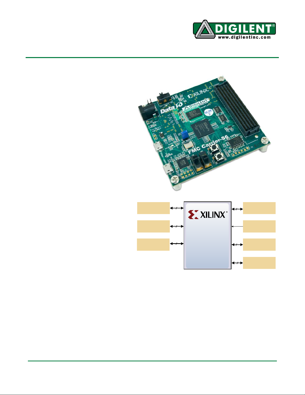
Overview
The FMC Carrier-S6 circuit board is a
digital circuit development platform based
on a Xilinx Spartan-6 LX45 FPGA. The
large FPGA along with the high-pin count
FMC socket, 128MByte DDR2 on-board
memory, and compact PCB size make
this an ideal FMC Host controller board for
embedded processor designs based on
Xilinx’s MicroBlaze.
FMC Carrier-S6 is compatible with all
Xilinx CAD tools, including ChipScope,
EDK, and the free ISE WebPack™, so
designs can be completed at no extra
cost.
The Spartan-6 LX45 is optimized for highperformance logic and offers:
6,822 slices, each containing four 6-
input LUTs and eight flip-flops
2.1Mbits of fast block RAM
four clock tiles (eight DCMs & four
PLLs)
58 DSP slices
500MHz+ clock speeds
The FMC Carrier-S6 board includes
Digilent's Adept USB2 system, which
offers device programming and user-data
transfer facilities.
Doc: 502-256 page 1 of 7
Copyright Digilent, Inc. All rights reserved. Other product and company names mentioned may be trademarks of their respective owners.
Page 2
FMC Carrier-S6 Reference Manual
M0
M1
JTAG
Port
USB
Controller
Numonyx SPI
Flash (x4)
16Mbytes
SPI
Port
J2
Adept USB Port
Spartan-6
JP2
Done
Load to enable
boot from ROM
FT232HQ
J3
UART Port
Serial
Port
2
3V3
Features
Xilinx Spartan-6 LX45 FPGA, 324-pin BGA package
128Mbyte DDR2 with 16-bit wide data
on-board USB2 port for programming and data transfer
USB-UART
16Mbyte x4 SPI Flash for configuration and data storage
100MHz Oscillator
Over 120 GPIO signals available through FMC HPC
GPIO includes 2 LEDs, 2 buttons, and 2 slide switches
ships with 12V power supply and USB cable
Configuration
After power-on, the
FPGA on the FMC
Carrier – S6 board must
be configured (or
programmed) before it
can perform any
functions. The FPGA
can be configured in two
ways: a USBconnected PC can
configure the board
using the JTAG port any
time power is on and a
configuration file stored
in the SPI Flash ROM
can be automatically
transferred to the FPGA
at power-on.
An on-board mode jumper (JP2) selects between JTAG/USB and ROM programming modes. If JP2 is
loaded, the FPGA will automatically configure itself from the ROM. If JP2 is not loaded, the FPGA will
remain idle after power-on until configured from the JTAG port.
Both Digilent and Xilinx freely distribute software that can be used to program the FPGA and the SPI
ROM. Programming files are stored within the FPGA in SRAM-based memory cells. This data defines
the FPGA’s logic functions and circuit connections, and it remains valid until it is erased by removing
power or asserting the PROG_B input, or until it is overwritten by a new configuration file.
FPGA configuration files transferred via the JTAG port use the .bit or .svf file types. Xilinx’s ISE
WebPack and EDK software can create .bit, .svf, .bin, or .mcs files from VHDL, Verilog, or schematicbased source files (EDK is used for MicroBlaze™ embedded processor-based designs).
www.digilentinc.com page 2 of 7
Copyright Digilent, Inc. All rights reserved. Other product and company names mentioned may be trademarks of their respective owners.
Page 3

FMC Carrier-S6 Reference Manual
FMC Carrier - S6 VADJ Levels
SET_VADJ1
SET_VADJ0
VADJ Voltage
0 0 1.2V
0 1 1.8V
1 0 2.5V
1 1 3.3V
FMC Carrier - S6 Power Supplies
Supply
Circuits
Device
Amps (max)
12V
FMC VCC12V0
IC15: ADP1850
5A
3.3V
FPGA I/O, USB ports, clocks, ROM
IC15: ADP1850
4A
1.8V
FPGA aux, GPIO
IC15: ADP1850
1A
1.23V
FPGA core
IC23: LTC3546
3A
VADJ
1V2, 1V8, 2V5, 3V3
IC23: LTC3413
4.2A
Adept and iMPACT USB Port
The Adept port is compatible with Xilinx's iMPACT programming software if the Digilent Plug-In for
Xilinx Tools is installed on the host PC (download it free from the Digilent website’s software section).
The plug-in automatically translates iMPACT-generated JTAG commands into formats compatible
with the Digilent USB port, providing a seamless programming experience without leaving the Xilinx
tool environment. Once the plug-in is installed, the "third party" programming option can be selected
from the iMPACT tools menu, and iMPACT will work as if a Xilinx programming cable were being
used. All Xilinx tools (iMPACT, ChipScope, EDK, etc.) can work with the plug-in, and they can be
used in conjunction with Adept tools.
Adept’s high-speed USB2 system can be used to program the FPGA and ROM and exchange
register-based and file-based data with the FPGA. The Adept application, an SDK, and reference
materials are freely downloadable from the Digilent website.
Power Supplies
The FMC Carrier - S6 board requires an external 12V, 5A or greater power source with a coax centerpositive 2.1mm internal-diameter plug (a suitable supply is provided as a part of the FMC Carrier - S6
kit). Voltage regulator circuits from Analog Devices create the required 3.3V, 1.8V, 1.23V and VADJ
supplies from the main 12V supply. The table below provides additional information, typical currents
depend strongly on FGPA configuration, and the values provided are typical of medium-size/speed
designs).
A power-good LED (LD3), driven by the wired-OR of all the power-good outputs on the supplies,
indicates that all supplies are operating within 10% of nominal.
The VADJ rail has to be enabled by logic implemented in the FPGA. To do this, set the SET_VADJ0
and SET_VADJ1 pins to indicate the desired voltage and drive VADJ_EN high. It is important to note
that FPGA banks 0 and 1 are unpowered whenever VADJ_EN is low. The table below outlines the
different voltages that may be selected:
www.digilentinc.com page 3 of 7
Copyright Digilent, Inc. All rights reserved. Other product and company names mentioned may be trademarks of their respective owners.
Page 4

FMC Carrier-S6 Reference Manual
Address
A12:
G6
A4:
F3
A11:
D3
A3:
L7
A10:
F4
A2:
H5
A9:
D1
A1:
J6
A8:
D2
A0:
J7
A7:
H6
A6:
H3
A5:
H4
Data
D15:
U1
D7:
J1
D14:
U2
D6:
J3
D13:
T1
D5:
H1
D12:
T2
D4:
H2
D11:
N1
D3:
K1
D10:
N2
D2:
K2
D9:
M1
D1:
L1
D8:
M3
D0:
L2
DQ[15:0]
13
16
AD[12:0]
RAS#
CAS#
WE#
BA0
BA1
BA2
See Table
CS#
L4
P1
P2
E1
F1
F2
E3
K5
L5
Spartan-6
DDR2
VREF
CKE
CK
CK#
UDQS_P
UDQS_N
LDQS_P
LDQS_N
UDM
LDM
ODT
1V8
L3
K4
K3
K6
H7
G1
G3
DDR2 Memory
A single 1Gbit DDR2 memory chip is driven from the memory controller block in the Spartan-6
FGPA. The DDR2 device, a Micron MT47H64M16-25E or equivalent, provides a 16-bit bus and 64M
locations. The FMC Carrier - S6 board has been tested for DDR2 operation at up to an 800MHz data
rate.
The DDR2 interface follows the pinout and routing guidelines specified in the Xilinx Memory Interface
Generator (MIG) User Guide. The interface supports SSTL18 signaling, and all address, data, clocks,
and control signals are delay-matched and impedance-controlled. Address and control signals are not
terminated. Two well-matched DDR2 clock signal pairs are provided so the DDR can be driven with
low-skew clocks from the FPGA.
www.digilentinc.com page 4 of 7
Copyright Digilent, Inc. All rights reserved. Other product and company names mentioned may be trademarks of their respective owners.
Page 5

FMC Carrier-S6 Reference Manual
T10
TXD
U10
Micro-USB
J3
“UART”
2
RXD
Spartan-6
FT232HQ
CS#
SDI/DQ0
SDO/DQ1
R15
R13
T13
V3
Spartan-6 SPI Flash
WP#/DQ2
HLD#/DQ3
T14
V14
SCK
Flash Memory
The FMC Carrier - S6 board uses a 128Mbit Numonyx
N25Q128 Serial Flash memory device (organized as 16-bit
by 16Mbytes) for non-volatile storage of FPGA
configuration files. The SPI Flash can be programmed with
a .bit, .bin., or .mcs file using the Adept software. An FPGA
configuration file requires less than 12Mbits, leaving
116Mbits available for user data. Data can be transferred
from a PC to/from the Flash by user applications, or by
facilities built into the Adept software. User designs
programmed into the FPGA can also transfer data to and
from the ROM.
A simple demo image has been loaded into the Serial Flash during manufacturing. It connects the
User LEDs (LD0, LD1) to the User Switches (SW0, SW1). The image along with the project source is
available on the Digilent website.
Oscillators/Clocks
The FMC Carrier - S6 board includes a single 100MHz Oscillator connected to pin T9 (T9 is a GCLK
input in bank 2). The input clock can drive any or all of the four clock management tiles in the Spartan-
6. Each tile includes two Digital Clock Managers (DCMs) and one Phase-Locked Loop (PLL).
DCMs provide the four phases of the input frequency (0º, 90º, 180º, and 270º), a divided clock that
can be the input clock divided by any integer from 2 to 16 or 1.5, 2.5, 3.5... 7.5, and two antiphase
clock outputs that can be multiplied by any integer from 2 to 32 and simultaneously divided by any
integer from 1 to 32.
PLLs use Voltage Controlled Oscillators (VCOs) that can be programmed to generate frequencies in
the 400MHz to 1080MHz range by setting three sets of programmable dividers during FPGA
configuration. VCO outputs have eight equally-spaced outputs (0º, 45º, 90º, 135º, 180º, 225º, 270º,
and 315º) that can be divided by any integer between 1 and 128.
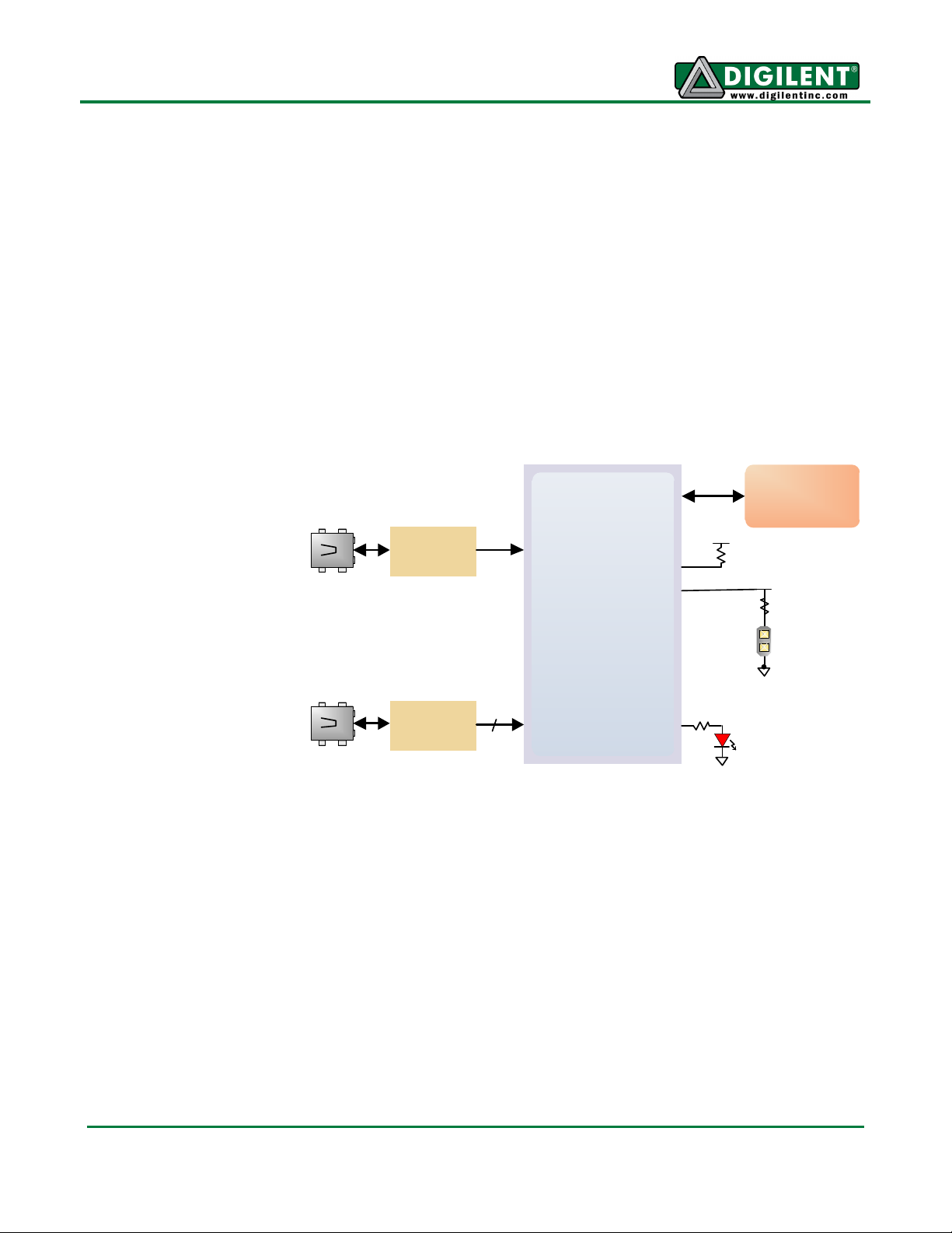
USB-UART Bridge (Serial Port)
The FMC Carrier - S6 includes an FTDI USB-UART bridge to allow PC applications to communicate
with the board using a COM port. Free drivers allow COM-based (i.e., serial port) traffic on the PC to
be seamlessly transferred to the FMC
Carrier – S6 board using the USB
port at J3 marked UART. The FTDI
part delivers the data to the Spartan6 using a two-wire serial port with
software flow control (XON/XOFF).
Free Windows and Linux drivers can
be downloaded from
www.ftdichip.com. After the drivers are installed, I/O commands from the PC directed to the COM
port will produce serial data traffic on the T10 and Q10 FPGA pins.
www.digilentinc.com page 5 of 7
Copyright Digilent, Inc. All rights reserved. Other product and company names mentioned may be trademarks of their respective owners.
Page 6

FMC Carrier-S6 Reference Manual
Spartan-6
Slide Switches
10K
10K
10K
LEDs
390
2
2
2
Pushbuttons
Pushbuttons
Slide Switches
LEDs
BTNU:
E4
SW0:
U7
LD0:
V15
BTND:
F5
SW1:
V7
LD1:
N12
Basic I/O
The FMC Carrier - S6 board includes two pushbuttons, two slide switches, and two LEDs for basic
digital input and output. The buttons and slide switches are connected to the FPGA via series
resistors to prevent damage from inadvertent short circuits. The high efficiency LED anodes are
connected to the FPGA via 390-ohm resistors, and they will brightly illuminate with about 1mA of
current when a logic high voltage is applied to their respective I/O pin.
FMC-HPC Connector
A single high-pin count (HPC) FMC slot is provided on the FMC Carrier – S6 to support a large
ecosystem of plug-in modules. The FMC exposes 126 single-ended I/O, 102 of which can be
configured as 51 differential pairs. The FMC interface spans over 4 PL I/O banks (banks 0, 1, 2, and
Misc.). The FMC pin-out can be found in the FMC Carrier – S6 General UCF file.
Quality Assurance
All FMC Carrier - S6 boards are 100% tested during the manufacturing process. If any device on the
FMC Carrier - S6 board fails test or is not responding properly, it is likely that damage occurred during
transport or during use. Typical damage includes stressed solder joints and contaminants in switches
and buttons resulting in intermittent failures. Stressed solder joints can be repaired by reheating and
reflowing solder and contaminants can be cleaned with off-the-shelf electronics cleaning products. If a
board fails test within the warranty period, it will be replaced at no cost. If a board fails test outside of
the warranty period and cannot be easily repaired, Digilent can repair the board or offer a discounted
replacement. Contact Digilent for more details.
www.digilentinc.com page 6 of 7
Copyright Digilent, Inc. All rights reserved. Other product and company names mentioned may be trademarks of their respective owners.
Page 7

FMC Carrier-S6 Reference Manual
Appendix 1: Analog Devices Components
ADG3308 – Low Voltage, 8-channel Bidirectional Logic Level Translators
http://www.analog.com/ADP3308
ADG719 – CMOS MUX/SPDT Switch
http://www.analog.com/ADG719
ADP1850 – Dual DC-to-DC Synch Buck Controller
http://www.analog.com/ADP1850
ADG804 – Low Voltage 4V, 4-Channel Multiplexer
http://www.analog.com/ADG804
www.digilentinc.com page 7 of 7
Copyright Digilent, Inc. All rights reserved. Other product and company names mentioned may be trademarks of their respective owners.
 Loading...