

Page 1

Digilent PmodAD5™ Analog to
Digital Voltage Converter
Revision: January 24, 2013
Note: This document applies to REV A of the board
Overview
The PmodAD5 is a high resolution analog-todigital converter built around the Analog
Devices AD7193 Sigma-Delta ADC.
Features include:
• SPI communication interface
• 24-bit resolution
• fast settling filter
• conversion synchronization
• five filter options
• four differential analog inputs or eight
pseudo-differential inputs
• two SMA connector inputs
Functional Description
The PmodAD5 has ten analog inputs that
correspond to eight data lines. The two SMA
female connectors route to inputs one and two,
while eight standard female header pins route
to inputs one through eight.
Customers can set the PmodAD5 into single or
continuous conversion mode. The PmodAD5
powers up by default in continuous conversion
mode. You can set the mode to start a
conversion by either writing to the appropriate
registers or on the rising edge of SYNC.
Note: Please see the AD7193 data sheet,
available from www.analog.com, for more
detailed information on controlling the A/D
Converter.
Serial Interface
The PmodAD5 has a 4-wire SPI
communication interface. (See Table 1 for
signal descriptions.)
1300 Henley Court | Pullman, WA 99163
(509) 334 6306 Voice and Fax
Analog Inputs
The analog inputs (AIN) on the PmodAD5 are
configurable as four differential inputs or as
eight pseudo-differential inputs. AINCOM
serves as a common reference for AIN
channels 1 through 8 under the eight pseudodifferential input configuration setting.
When operating the PmodAD5 analog inputs
as four differential inputs, the adjacent inputs
correspond to positive and negative differential
signals. For example, AIN1/ AIN2 represent
one positive/negative differential pair and
AIN3/AIN4 represent the second
positive/negative differential pair.
Connectors J5 and J6 are SMA female analog
inputs that correspond to AIN1 and AIN2
respectively.
Reference Supply and GPO
The PmodAD5 has a maximum of four general
purpose output (GPO) signals. Operators can
access these signals from headers J2 or J3.
Please see Table 1 for signal descriptions.
GPO pins 1 and 0 also correspond to REFIN2+
and REFIN2-. These pins can be configured to
supply the conversion/calibration reference
voltage for the PmodAD5.
Doc: 502-243 page 1 of 2
Copyright Digilent, Inc. All rights reserved. Other product and company names mentioned may be trademarks of their respective owners.
Page 2
PmodAD5 Reference Manual
J1-06
J2-08
J4-01
The PmodAD5 uses the 2.5VDC reference
present on REFIN1+ and REFIN2- by default.
Note: Please see the PmodAD5 schematic,
available from www.digilentinc.com, for more
detailed information on GPO and Reference
Supply routing.
Synchronization
Setting the SYNC pin to a logic low puts the
PmodAD5 in a standby state. Once you set the
pin to logic high, the PmodAD5 will begin
gathering samples. The conversion mode
(either single or continuous) must be set
previously.
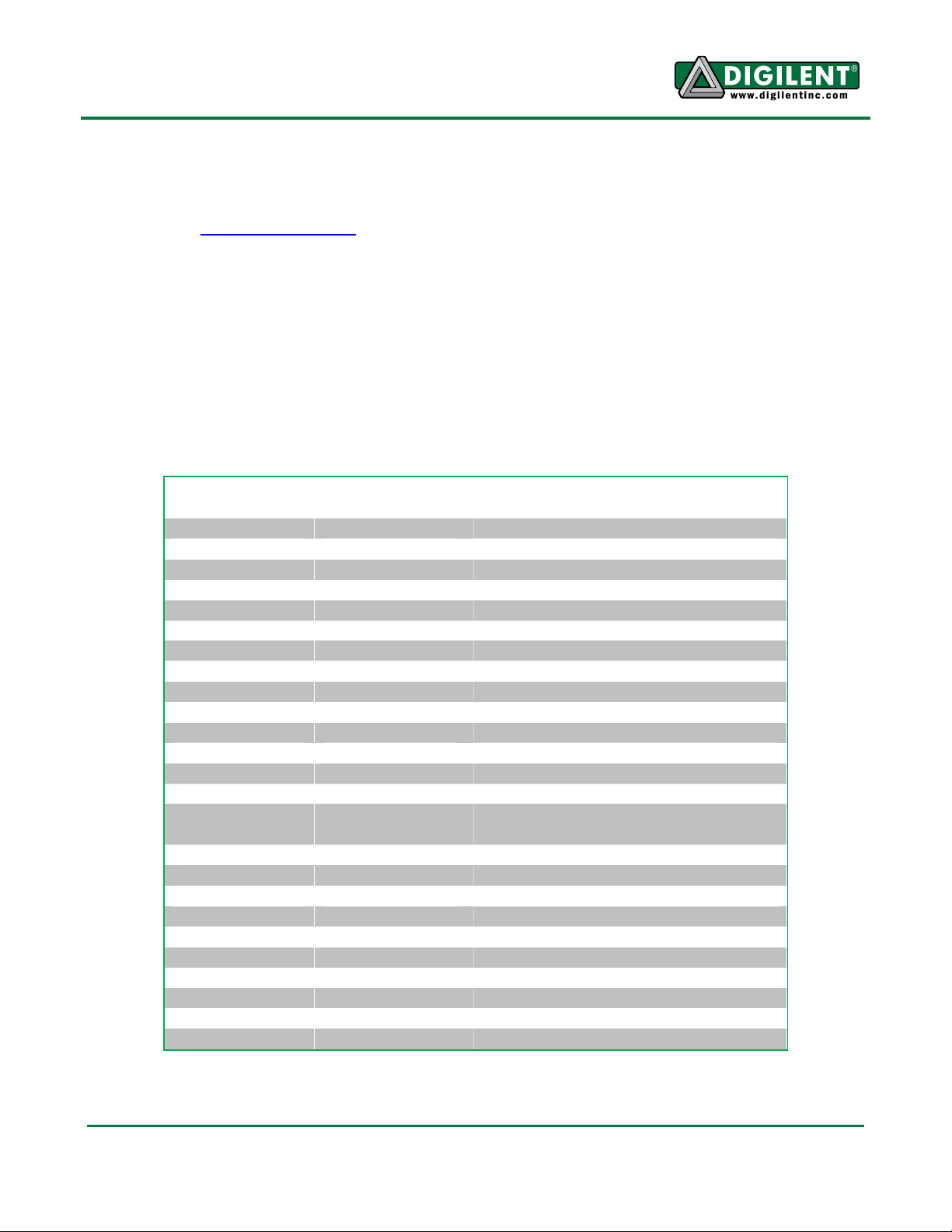
Connector Pin # Pin Name Description
Bridge Power Down Switch
Operators can use the bridge power down
switch to control external circuitry driving the
analog inputs. Closing this “switch” internally
ties the BPDSW signal to ground.
Analog Supply Voltage
Customers can connect an analog supply
voltage at header J4, if JP1 remains open. You
must keep this external voltage between 3.0V
and 5.25V to avoid damaging your device.
J1-01
J1-02
J1-03
J1-04
J1-05
J2-01
J2-02
J2-03
J2-04
J2-05
J2-06
J2-07
J2-09
J2-10
J2-11
J2-12
J3-01
J3-02
J3-03
J4-02
J5
J6
CS SPI Chip Select. Connect to host ~SS
DIN SPI Data In. Connect to host SDO
DOUT/RDY SPI Data Out. Connect to host SDI
SCLK SPI Clock. Connect to host SCK
GND Ground
DVDD Digital Vdd
AIN1 Analog Input 1
AIN2 Analog Input 1
AIN3 Analog Input 1
AIN4 Analog Input 1
AIN5 Analog Input 1
AIN6 Analog Input 1
AIN7 Analog Input 1
AIN8 Analog Input 1
AINCOM
Analog Input Common, used for
pseudo differential signaling with AIN8:1
REFIN2+/P1 Positive Reference Input/GPO1.
REFIN2-/P0 Negative Reference Input/GP0.
BPDSW Bridge Power Down Switch.
SYNC Synchronization control
P2 GPO2
P3 GPO3
AVDD Analog Vdd
GND Ground
AIN1 SMA input 1
AIN2 SMA input 2
Table 1. Connector Pinout Tables
www.digilentinc.com page 2 of 2
Copyright Digilent, Inc. All rights reserved. Other product and company names mentioned may be trademarks of their respective owners.
 Loading...