

Page 1
PPmmooddIIOOXXPP™™ RReeffeerreennccee MMaannuuaal
Connector J3
– I2C Communications
Pin Signal
Description
l
Revision: August 24, 2011
Overview
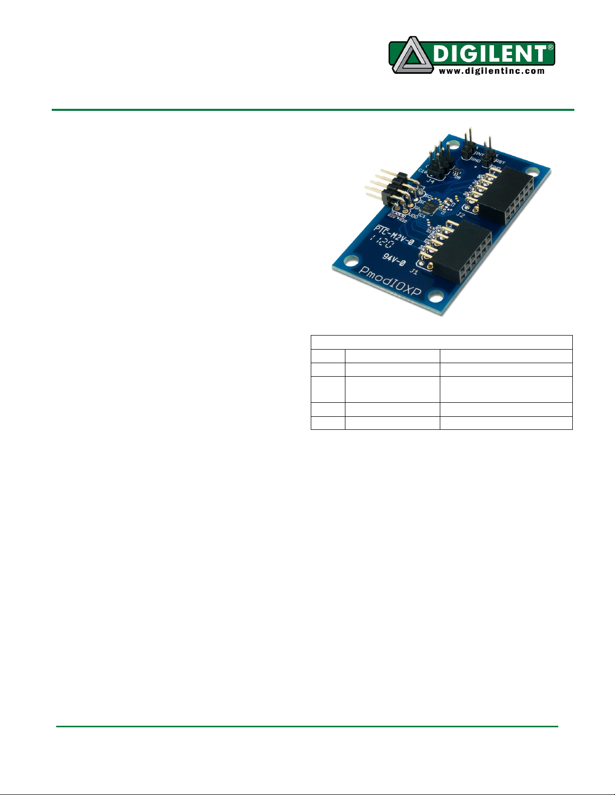
The PmodIOXP is an I/O expansion module
powered by the Analog Devices ADP5589.
Features include:
• 16-element FIFO for event recording
• 19 configurable I/Os
• Keypad decoding for matrices up to
11x8
• PWM generator
• Open-drain interrupt output
• Dual Programmable logic blocks
• Debouncing on IOs
• I2C interface
Functional Description
The PmodIOXP functions as an I/O port
expander and keypad matrix decoder. The
PmodIOXP uses a standard 8-pin I2C
connector and can communicate to a system
board via I2C.
Interface
All communications with the device must
specify a register address and a flag indicating
whether the communication is a read or a
write. This is followed by the actual data
transfer.
Device configuration is performed by writing to
control registers within the device. Input and
event data is accessed by reading certain
device registers.
A full list of registers and their functionality, as
well as communication specifications, is found
in the ADP5589 datasheet available on the
Analog Devices website.
1300 NE Henley Court, Suite 3
(509) 334 6306 Voice | (509) 334 6300 Fax
1, 2 SCLK Serial Clock
3, 4 SDA / SDI /
SDIO
5, 6 GND Power Supply Ground
7, 8 VCC Power Supply (3.3V)
Pullman, WA 99163
I2C Data / SPI Master
out Slave in Data
Interface Connector Signal Description
The I2C interface standard uses two signal
lines. These are I2C data (SDA) and serial
clock (SCLK). These signals map to the serial
data (SDA) and serial clock (SCLK)
respectively on the ADP5589.
Event FIFO
The PmodIOXP has an event FIFO that can
record up to 16 events. The FIFO includes key
events and can be configured to include
general-purpose input (GPI) and logic activity.
When the FIFO is read from, the first entry is
always read. Specific registers related to the
FIFO are outlined in the ADP5589 datasheet.
Doc: 502-219 page 1 of 2
Copyright Digilent, Inc. All rights reserved. Other product and company names mentioned may be trademarks of their respective owners.
Page 2
PmodIOXP Reference Manual
Connector J5
Pin Signal
Description
Connector J
6
Pin Signal
Description
Connector J4
-
GPIOs
Pin Signal
Description
Connector J1
-
GPIOs
Pin Signal
Description
Connector J2
-
GPIOs
Pin Signal
Description
1 INT Interrupt Open Drain Output
2 GND Power Supply Ground
Open-Drain Interrupt Output
The interrupt pin can be configured to trigger
on an event, GPI level, FIFO overflow, logic
function output, and on keyboard lock. The
corresponding bit in the interrupt enable
register must be set in order for the interrupt to
be set. Specific registers related to the
interrupts are described in the ADP5589
datasheet.
1 RST Reset pin
2 GND Power Supply Ground
Reset Pin
The PmodIOXP has an active-low reset pin
that can be used to reset the ADP5589 to
default settings.
General Purpose I/O (GPIO)
The PmodIOXP has 19 GPIOs that can be
configured a number of ways. The GPIOs can
be set as either input or output, set to decode a
keypad matrix, or implement logic functions.
The functionality of the IOs can be set using
the configuration registers which are described
in the ADP5589 datasheet.
1 R0 Row 0 (GPIO 1)
2 R1 Row 1 (GPIO 2)
3 R2 Row 2 (GPIO 3)
4 R3 Row 3 (GPIO 4)
5 GND Power Supply Ground
6 VCC Power Supply(3.3V)
7 C0 Column 0 (GPIO 9)
8 C1 Column 1 (GPIO 10)
9 C2 Column 2 (GPIO 11)
10 C3 Column 3 (GPIO 12)
11 GND Power Supply Ground
12 VCC Power Supply(3.3V)
1 R4 Row 4 (GPIO 5)
2 R5 Row 5 (GPIO 6)
3 R6 Row 6 (GPIO 7)
4 R7 Row 7 (GPIO 8)
5 GND Power Supply Ground
6 VCC Power Supply(3.3V)
7 C4 Column 4 (GPIO 13)
8 C5 Column 5 (GPIO 14)
9 C6 Column 6 (GPIO 15)
10 C7 Column 7 (GPIO 16)
11 GND Power Supply Ground
12 VCC Power Supply(3.3V)
1 C8 Column 8 (GPIO 17)
2 GND Power Supply Ground
3 C9 Column 9 (GPIO 18)
4 GND
Power Supply Ground
5 C10 Column 10 (GPIO 19)
6 GND Power Supply Ground
www.digilentinc.com page 2 of 2
Copyright Digilent, Inc. All rights reserved. Other product and company names mentioned may be trademarks of their respective owners.
 Loading...