

Page 1
cchhiippKKIITT™™ BBaassiicc II//OO SShhiieelldd
BBooaarrdd RReeffeerreennccee MMaannuuaal
l
Revision: July 16, 2011
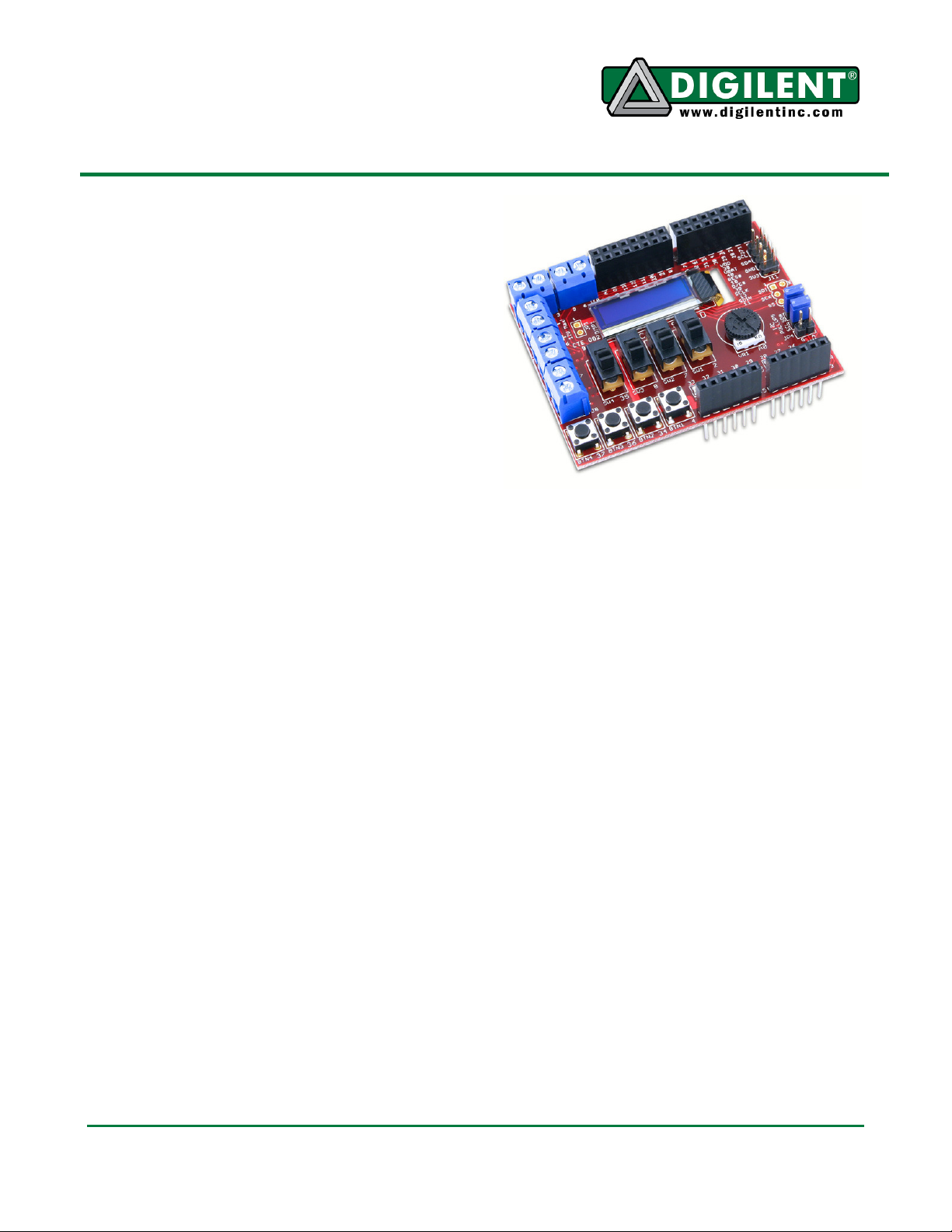
Overview
The chipKIT Basic I/O Shield is a input/output
expansion board designed for use with chipKIT
microcontroller boards such as the Uno32™
and the Max32™.
The Basic I/O Shield is designed to provide a
range of input/output devices suitable for
beginners learning about microcontrollers and
various types of I/O devices, or for use by
more advanced user to provide inputs or
outputs for their own projects.
The Basic I/O Shield provides simple digital
input devices such as switches and buttons,
and digital output devices such as discrete
LEDs and high current open FET drivers. It
provides more advanced devices such as an
I2C EEPROM, an I2C temperature sensor, and
organic LED graphic display. A potentiometer
is also provided for use as an analog input
device.
The Basic I/O Shield is designed to the same
form factor as the Uno32 board, but is also
useable with the Max32 board.
Features:
128x32 pixel OLED graphic display
I2C temperature sensor
256Kbit I2C EEPROM
I2C daisy chain connector
4 push buttons
4 slide switches
8 discrete LEDs
4 open drain FET drivers
Analog potentiometer
1300 NE Henley Court, Suite 3
Pullman, WA 99163
(509) 334 6306 Voice | (509) 334 6300 Fax
Doc: 502-216 page 1 of 15
Copyright Digilent, Inc. All rights reserved. Other product and company names mentioned may be trademarks of their respective owners.
Page 2
chipKIT Basic I/O Shield Reference Manual
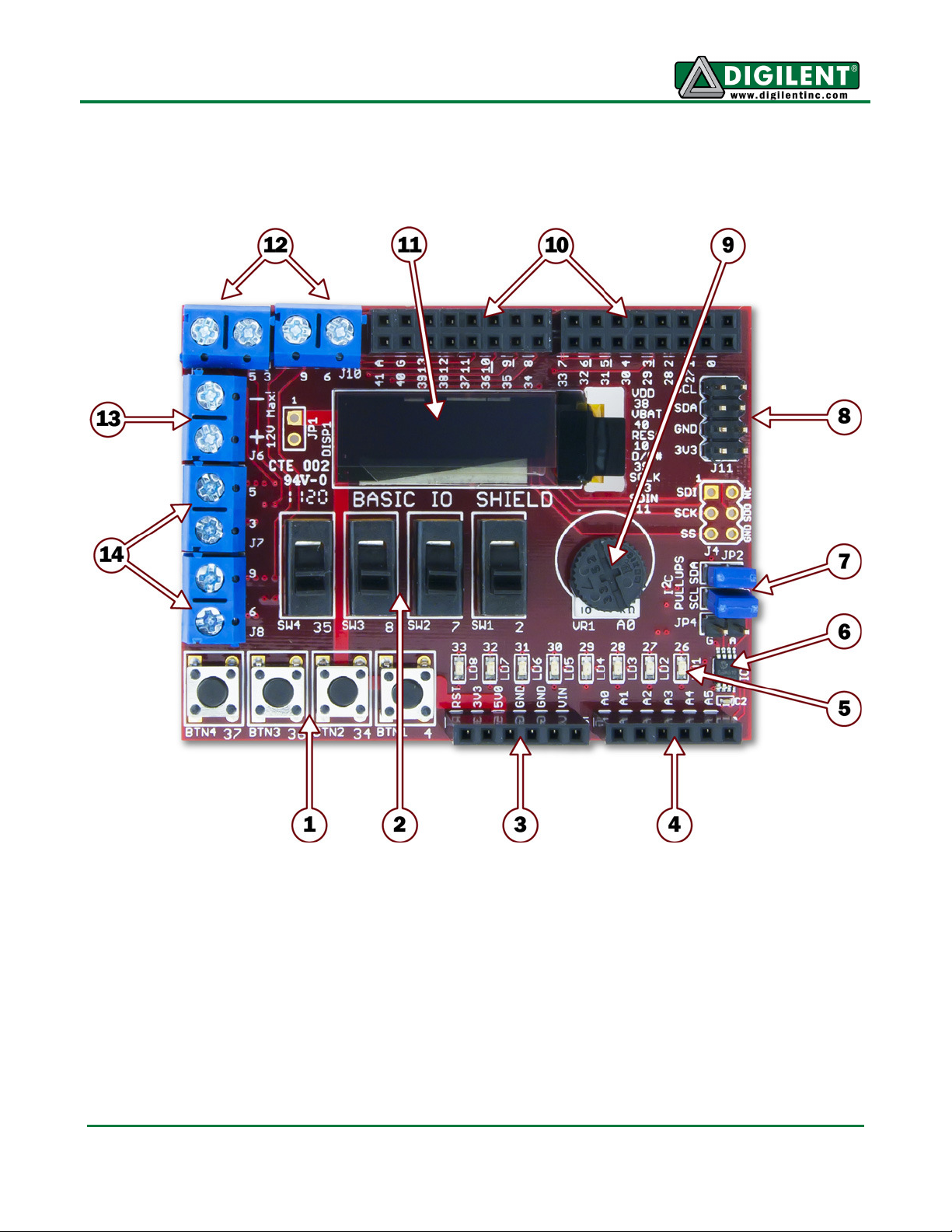
chipKIT Basic I/O Shield Hardware Overview
The Basic I/O Shield has the following hardware features:
1) Push Buttons
Four push buttons provide momentary contact discrete digital inputs. These can be
accessed using the
digitalRead
function.
2) Slide switches
Four slide switches that provide discrete digital inputs. These can be accessed using the
digitalRead
function.
3) J2 – Shield Power Connector
This connector powers the board, receiving power from the chipKIT microcontroller board.
www.digilentinc.com page 2 of 15
Copyright Digilent, Inc. All rights reserved. Other product and company names mentioned may be trademarks of their respective owners.
Page 3

chipKIT Basic I/O Shield Reference Manual
4) J3 – Analog Signal Connector
Pin 1 (analog signal A0) is connected to a potentiometer. Pins 5 and 6 (labeled as A4 and
A5) provide access to the I2C signals SDA and SCL for the I2C bus. The I2C bus is used to
access the temperature sensor and the EEPROM and for the I2C daisy chain connector.
Note: On the Uno32 it is necessary to set jumpers JP6 & JP7 to the correct position for
accessing the I2C signals on that board. On the Max32 board, it is necessary to use jumper
wires to bring the I2C signals onto the board, as the connector providing the I2C bus on the
Max32 board doesn’t contact the Basic I/O Shield.
5) Discrete LEDs
Eight LEDs that provide discrete digital outputs. These can be accessed individually using
the
digitalWrite
function. The LEDs are connected to the low eight bits of microcontroller
PORTE and all eight can be written at the same time by writing to PORTE.
6) IC2 – Temperature Sensor
This is a Microchip TCN75A digital temperature sensor. It is accessed via the I2C bus.
7) JP2/JP3 – I2C Pull-up Resistor Enable Jumpers
These jumpers are used to enable or disable the presence of the I2C pull-up resistors on
the I2C bus. Having the shorting blocks installed enables the resistors. Removing the
shorting blocks disables them.
8) J11 – I2C Daisy Chain Connector
This is a 2x4 pin header connector that provides access to the I2C signals SDA and SCL
as well as power from the 3.3V power bus and ground. This can be used to extend the I2C
bus off of the board and to power external I2C device. Digilent has cables and a selection
of I2C peripheral modules that can be accessed using this connector.
9) Potentiometer
This is a 10K ohm potentiometer connected across VCC3V3 and ground. It provides an
analog input voltage to analog input A0.
10) J1 and J2 – Digital Signal Connectors
These connectors bring digital signals from the chipKIT microcontroller board onto the
Basic I/O Shield board.
11) Organic LED Graphic Display
This is a 128x32 pixel monochrome OLED graphic display panel. This display panel is
accessed using the SPI interface.
12) J9 & J10 – Digital I/O Signal Connectors
These are screw terminal connectors that provide access to digital I/O signals 3, 5, 6, and
9. These are four of the PWM signals from the chipKIT microcontroller board.
13) J6 – Open Drain FET Power Connector
This provides access to the power connections for the open drain FETs.
14) , J7, & J8 – Open Drain FET Output
These provide access to the outputs of the open drain FETs.
www.digilentinc.com page 3 of 15
Copyright Digilent, Inc. All rights reserved. Other product and company names mentioned may be trademarks of their respective owners.
Page 4

chipKIT Basic I/O Shield Reference Manual
chipKIT Basic I/O Shield Hardware Description
Introduction
The following gives a basic description of the
input/output hardware contained in the Basic
I/O Shield and how to use it. Refer to Appendix
A for a table showing pin definitions, and
Appendix B for example code to use the OLED
graphic display.
OLED Graphic Display
The Basic I/O board provides a 128x32 pixel,
Organic LED (OLED), graphic display panel.
The graphic display panel used is the
WiseChip/Univision UG-23832HSWEG04. This
display uses the Soloman Systech SSD1306
display controller.
The UG2832 has a power on/power off
sequence that should be followed. Failure to
follow the power on/power off sequence can
shorten the life of the display. The Basic I/O
provides two FETs for software control of the
two power supplies for the display. The
VDD_EN control is used to turn on/off the
power to the logic of the display. The
VBAT_EN control is used to turn on/off power
to the OLED display itself. These two pins
have pull-up resistors to turn off their
respective power supplies when not being
driven. The pin is made an output and driven
low to turn on the power supply.
Power on sequence:
Apply power to VDD
Send Display Off command
Initialize display to desired operating mode
Clear screen
Apply power to VBAT
Delay 100ms
Send Display On command
Power off sequence:
Send Display Off command
Power off VBAT
Delay 100ms
Power off VDD
The display has a D/C pin (display or
command select) that is used to determine
whether bytes sent to the display are
interpreted as commands or as display data.
The D/C pin is set HIGH for display buffer
access and LOW for command access.
The RES pin is used to reset the SG1306
display controller. The RES pin is driven LOW
for reset and driven HIGH for normal operation.
The low going reset pulse must be a minimum
of 3us (microseconds) for the display controller
to reset correctly.
The UG2832 is a serial device that is accessed
using SPI. It is however, a write-only device. It
is not possible to read back either the display
buffer contents or any kind of status from the
panel. The maximum SPI clock frequency
supported by the UG2832 is 10Mhz. Due to pin
limitations between the Basic I/O and the
Uno32 board, the select pin (SS) is wired low
on the Basic I/O board and the display is
always enabled to receive data over the SPI
interface.
Digilent has a library for use with the Basic I/O
that provides functions for initializing the
display and rendering simple text and graphics
onto the display. This library can be used as-is
or as a starting point for a more sophisticated
graphics library. This library is available on the
Digilent web site and in the third part libraries
repository on github.
Appendix B provides example code that shows
initializing the display and writing to it.
www.digilentinc.com page 4 of 15
Copyright Digilent, Inc. All rights reserved. Other product and company names mentioned may be trademarks of their respective owners.
Page 5

chipKIT Basic I/O Shield Reference Manual
Discrete Digital I/O Devices
The Basic I/O Shield provides various discrete
digital I/O devices. These can be accessed
using the
functions. The
the pin to input or output.
When the buttons and switches on the Basic
I/O are not being used, the pins are available
on the pass-through shield connectors for use
by other shields in the stack. The pins used by
the LEDs are also available, however the
presence of the LEDs on the lines will load
them down, possibly causing some devices to
not work. It is safe to use any of these pins as
either inputs or outputs.
Push Buttons: There are four push buttons
switches labeled BTN1 (pin 4), BTN2 (pin 34),
BTN3 (pin 36), and BTN4 (pin 37). The
digitalRead
button is not pressed and
button is pressed.
Slide Switches: There are four slide switches
labeled SW1 (pin 2), SW2 (pin 7), SW3 (pin 8)
and SW4 (pin 35). The
return
the push buttons) and
up (toward the OLED display).
LEDs: There are eight LEDs, labeled LD1 –
LD8 accessed as digital pins 33 – 26. An LED
will be illuminated when the corresponding pin
is set to the
function and off when set to the
The LEDs are attached to the low eight bits of
PORTE, with LD1 connected to PORTE bit 0,
and LD8 connected to PORTE bit 7. An 8-bit
value written to PORTE (or LATE) will display
the corresponding binary value on the LEDs.
digitalRead
function will return
and
pinMode
digitalWrite
function is used to set
LOW
HIGH
when the
digitalRead
LOW
when the switch is down (toward
HIGH
when the switch is
HIGH
state using the
digitalWrite
LOW
if the
function will
state.
Open Drain FET Outputs
The Basic I/O provides four open drain FET
outputs. These are low-side N-channel devices
and can be used to provide a digital switch
closure to ground. These can be used to
switch external loads, such as relay coils,
solenoids, stepper motors, and so on.
The FETs used are the NTHD4508N. These
FETs are rated for a maximum VDS (voltage
from drain to source) of 20V. They are rated for
a maximum continuous current of 3.0A at 25ºC
and 2.2A at 85ºC. For more detailed
specifications for the FETs refer to the data
sheet available from the On Semiconductor
web site.
The FETs are labeled Q1A (pin 9), Q1B (pin
6), Q2A (pin 5), and Q2B (pin 3). These four
pins are also four of the PWM outputs
supported by the chipKIT boards and the FETs
can be switched using pulse width modulation
(PWM) using the
An FET is switched on by driving its gate high.
When the FET is on, it provides a low
impedance path to ground (similar to a closed
switch to ground). When the FET is switched
off by driving its gate low, it becomes a high
impedance path to ground (similar to an open
switch to ground). Pull-down resistors are
connected to the gate of each FET to ensure
that it is off unless being actively driven high by
the microcontroller on the chipKIT board.
The FET outputs are accessed via the screw
terminal connectors J7 and J8 on the left side
of the board. The digital signals used to switch
the FETs on and off are also available on
screw terminal connectors J9 and J10 at the
left side of the upper edge of the board.
A FET is used to switch an external load, such
as a relay coil, on and off. The load is wired
between the positive side of an external power
supply and the output of the FET. When the
FET is switched on, current will flow from the
external power supply through the load and the
FET to ground.
FETs are often used to switch highly inductive
loads, such as relay coils, solenoids, and
motors. When the current through an inductive
load is switched off, a voltage spike will occur
analogWrite
function.
www.digilentinc.com page 5 of 15
Copyright Digilent, Inc. All rights reserved. Other product and company names mentioned may be trademarks of their respective owners.
Page 6

chipKIT Basic I/O Shield Reference Manual
that can damage the FET. The Basic I/O
provides clamp diodes (also called snubber or
flyback diodes) to clamp the voltage spike and
feed the current back to the external supply.
Screw terminal connector J6 is used to provide
the power and ground connections back to the
external power supply. The negative (-) pin of
J6 connects the external supply ground with
the Basic I/O ground, and the positive (+)
terminal connects the Basic I/O to the external
supply voltage.
The unloaded two pin header JP1 can be used
to connect the board VCC5V0 power supply
bus to the external power supply bus so that
the board 5V supply can be used instead of an
external supply. In this case, J6 is used to
connect the board supply to the external loads.
If this is done, the total current consumed by all
external loads must not exceed 2A or the
current rating of the board power supply
(whichever is less).
I2C Bus
The I2C bus from the chipKIT microcontroller
board is brought onto the Basic I/O Shield.
There are two I2C devices on the board and a
connector for taking the I2C bus off of the
board to connect to additional external I2C
devices.
I2C Connector: Connector J11 can be used to
extend the I2C bus off of the board to connect
to additional external I2C devices. J11 is a
standard 2x4 pin header connector with 0.100”
spaced pins. It provides access to the I2C
signals, SCL and SDA, plus VCC3V3 and
ground. The VCC3V3 can be used to power
external I2C devices.
The I2C bus uses open collector drivers to
allow multiple devices to drive the bus signals.
This means that pull-up resistors must be
provided to supply the logic high state for the
signals. The Basic I/O provides 2.2Kohm pullup resistors. Generally, only one set of pull-up
resistors are used on the bus. Jumpers JP2
and JP3 can be used to disable the on-board
pull-up resistors if a different value is needed
or some other device on the bus is providing
the pull-ups. The on-board pull-up resistors are
enabled by install shorting blocks on JP2 and
JP3. Removing the shorting blocks disables
the pull-up resistors.
Digilent has several small I/O modules
available that can be connected using the I2C
connector. These include a 3-axis
accelerometer, 4-channel, 12-bit A/D
converter, serial character LCD panel, 3-axis
gyroscope, real-time clock/calendar, and I/O
expander.
EEPROM: A 256Kbit (32Kbyte), I2C EEPROM
is provided using a Microchip 24LC256. This
EEPROM, IC1, is located on the bottom left of
the board, just below the chipKIT logo.
The seven bit I2C device address for the
EEPROM is ‘1010000’.
Digilent provides a library for accessing this
EEPROM. The library is available on the
Digilent web site and in the third party libraries
repository on github.
For complete technical documentation on the
24LC256, refer to the data sheet available on
the Microchip web site.
Temperature Sensor: A digital temperature
sensor is provided using a Microchip TCN75A
2-Wire Serial Temperature Sensor. The
temperature sensor, IC2, is an I2C device, and
is located in the lower right corner of the board.
The TCN75A is rated for an accuracy of +/-1ºC
and has selectable resolution from 0.5ºC down
to 0.0625ºC. The seven bit device address is
‘1001000’.
Digilent provides a library for accessing the
temperature sensor. This library is available on
the Digilent web site and in the third party
library repository on github.
The TCN75A provides an alert output that can
be programmed for various functions. This
www.digilentinc.com page 6 of 15
Copyright Digilent, Inc. All rights reserved. Other product and company names mentioned may be trademarks of their respective owners.
Page 7

chipKIT Basic I/O Shield Reference Manual
output can be accessed using JP4, which is
adjacent to IC2.
For complete technical documentation on the
TCN75A, refer to the data sheet available on
the Microchip web site.
Potentiometer
A potentiometer (pot) is provided on the board
to be used as an analog signal source or
analog control input. The pot is a 10Kohm
trimmer pot connected between the VCC3V3
supply and ground. The wiper of the pot is
connected to analog input A0.
The pot is read using the
analogRead
function.
www.digilentinc.com page 7 of 15
Copyright Digilent, Inc. All rights reserved. Other product and company names mentioned may be trademarks of their respective owners.
Page 8

chipKIT Basic I/O Shield Reference Manual
Uno32
Max32
Function
Description
Notes
Appendix A: chipKIT Basic I/O Shield Pinout Table
pin #
10 10 RES OLED reset JP4 on Uno32
39 83 DC OLED data/command select
13 13 SCLK OLED serial clock
11 11 SDIN OLED serial data in JP7 on Uno32/JP4 on Max32
40 84 VBAT_EN OLED VBAT enable
38 82 VDD_EN OLED VDD enable
33 77 LD1 User LED
32 76 LD2 User LED
31 75 LD3 User LED
30 74 LD4 User LED
29 73 LD5 User LED
28 72 LD6 User LED
27 71 LD7 User LED
26 70 LD8 User LED
4 4 BTN1 Push button
34 78 BTN2 Push button
36 79 BTN3 Push button
37 80 BTN4 Push button
2 2 SW1 Slide switch
7 7 SW2 Slide switch
8 8 SW3 Slide switch
35 79 SW4 Slide switch
3 3 OC1 Open drain/PWM output
5 5 OC2 Open drain/PWM output
6 6 OC3 Open drain/PWM output
9 9 OC4 Open drain/PWM output
19 59 SCL I2C clock JP8 on Uno32/jumper wire on Max32
18 58 SDA I2c data JP6 on Uno32/jumper wire on Max32
14 54 A0 Potentiometer
pin #
www.digilentinc.com page 8 of 15
Copyright Digilent, Inc. All rights reserved. Other product and company names mentioned may be trademarks of their respective owners.
Page 9

chipKIT Basic I/O Shield Reference Manual
Appendix B: Example Driver Code
The following gives an example of code to initialize the display controller and write the contents of a
memory buffer into the display. This example is written for the chipKIT Uno32 board.
Symbol and Variable Declarations
/* ------------------------------------------------------------ */
/* Pin definitions for access to OLED control signals on chipKIT Uno32
*/
#define prtVddCtrl IOPORT_F
#define prtVbatCtrl IOPORT_F
#define prtDataCmd IOPORT_F
#define prtReset IOPORT_G
#define bitVddCtrl BIT_6
#define bitVbatCtrl BIT_5
#define bitDataCmd BIT_4
#define bitReset BIT_9
/* ------------------------------------------------------------ */
/* Symbols describing the geometry of the display.
#define cbOledDispMax 512 //max number of bytes in display buffer
#define ccolOledMax 128 //number of display columns
#define crowOledMax 32 //number of display rows
#define cpagOledMax 4 //number of display memory pages
/* ------------------------------------------------------------ */
/* This array is the off-screen frame buffer used for rendering.
** It isn't possible to read back from the OLED display device,
** so display data is rendered into this off-screen buffer and then
** copied to the display.
*/
BYTE rgbOledBmp[cbOledDispMax];
www.digilentinc.com page 9 of 15
Copyright Digilent, Inc. All rights reserved. Other product and company names mentioned may be trademarks of their respective owners.
Page 10

chipKIT Basic I/O Shield Reference Manual
PIC32 Hardware Initialization
The following function initializes the PIC32 hardware for talking to the display. It initializes the SPI
controller and sets the control pins to be outputs.
/* ------------------------------------------------------------ */
/*** OledHostInit
**
** Parameters:
** none
**
** Return Value:
** none
**
** Errors:
** none
**
** Description:
** Perform PIC32 device initialization to prepare for use
** of the OLED display.
** This example is hard coded for the chipKIT Uno32 and
** SPI2.
*/
void
OledHostInit()
{
unsigned int tcfg;
/* Initialize SPI port 2.
*/
SPI2CON = 0;
SPI2BRG = 15; //8Mhz, with 80Mhz PB clock
SPI2STATbits.SPIROV = 0;
SPI2CONbits.CKP = 1;
SPI2CONbits.MSTEN = 1;
SPI2CONbits.ON = 1;
/* Make pins RF4, RF5, and RF6 be outputs.
*/
PORTSetBits(IOPORT_F, bitVddCtrl|bitVbatCtrl|bitDataCmd);
PORTSetPinsDigitalOut(prtDataCmd, bitDataCmd); //Data/Command# select
PORTSetPinsDigitalOut(prtVddCtrl, bitVddCtrl); //VDD power control (1=off)
PORTSetPinsDigitalOut(prtVbatCtrl, bitVbatCtrl); //VBAT power control (1=off)
/* Make the RG9 pin be an output. On the Basic I/O Shield, this pin
** is tied to reset.
*/
PORTSetBits(prtReset, bitReset);
PORTSetPinsDigitalOut(prtReset, bitReset);
}
www.digilentinc.com page 10 of 15
Copyright Digilent, Inc. All rights reserved. Other product and company names mentioned may be trademarks of their respective owners.
Page 11

chipKIT Basic I/O Shield Reference Manual
Display Controller Initialization
The following function performs initialization of the display controller on the display panel. This
performs the power up sequence on the display and initializes it for a non-interleaved display buffer
with the origin in the upper left corner.
/* ------------------------------------------------------------ */
/*** OledDspInit
**
** Parameters:
** none
**
** Return Value:
** none
**
** Errors:
** none
**
** Description:
** Initialize the OLED display controller and turn the display on.
*/
void
OledDspInit()
{
/* We're going to be sending commands, so clear the Data/Cmd bit
*/
PORTClearBits(prtDataCmd, bitDataCmd);
/* Start by turning VDD on and wait a while for the power to come up.
*/
PORTClearBits(prtVddCtrl, bitVddCtrl);
DelayMs(1);
/* Display off command
*/
Spi2PutByte(0xAE);
/* Bring Reset low and then high
*/
PORTClearBits(prtReset, bitReset);
DelayMs(1);
PORTSetBits(prtReset, bitReset);
/* Send the Set Charge Pump and Set Pre-Charge Period commands
*/
Spi2PutByte(0x8D);
Spi2PutByte(0x14);
Spi2PutByte(0xD9);
Spi2PutByte(0xF1);
/* Turn on VCC and wait 100ms
*/
PORTClearBits(prtVbatCtrl, bitVbatCtrl);
DelayMs(100);
/* Send the commands to invert the display. This puts the display origin
** in the upper left corner.
*/
www.digilentinc.com page 11 of 15
Copyright Digilent, Inc. All rights reserved. Other product and company names mentioned may be trademarks of their respective owners.
Page 12

chipKIT Basic I/O Shield Reference Manual
Spi2PutByte(0xA1); //remap columns
Spi2PutByte(0xC8); //remap the rows
/* Send the commands to select sequential COM configuration. This makes the
** display memory non-interleaved.
*/
Spi2PutByte(0xDA); //set COM configuration command
Spi2PutByte(0x20); //sequential COM, left/right remap enabled
/* Send Display On command
*/
Spi2PutByte(0xAF);
}
www.digilentinc.com page 12 of 15
Copyright Digilent, Inc. All rights reserved. Other product and company names mentioned may be trademarks of their respective owners.
Page 13

chipKIT Basic I/O Shield Reference Manual
Display Memory Update
This function copies the contents of a 512 byte buffer from PIC32 memory to the display. The display
memory is organized as four pages of 128 bytes each. Each memory page corresponds to an eight
pixel high stripe across the display. Each byte in the memory page corresponds to an eight pixel high
column on the display. The least significant bit in a display byte is the top most pixel, and the most
significant bit the bottom most pixel. The first byte in the page corresponds to the left most pixels on
the display and the last byte the right most pixels.
This function assumes that the display buffer to be copied is the global variable
/* ------------------------------------------------------------ */
/*** OledUpdate
**
** Parameters:
** none
**
** Return Value:
** none
**
** Errors:
** none
**
** Description:
** Update the OLED display with the contents of the memory buffer
*/
void
OledUpdate()
{
int ipag;
int icol;
BYTE * pb;
pb = rgbOledBmp;
for (ipag = 0; ipag < cpagOledMax; ipag++) {
PORTClearBits(prtDataCmd, bitDataCmd);
/* Set the page address
*/
Spi2PutByte(0x22); //Set page command
Spi2PutByte(ipag); //page number
/* Start at the left column
*/
Spi2PutByte(0x00); //set low nybble of column
Spi2PutByte(0x10); //set high nybble of column
PORTSetBits(prtDataCmd, bitDataCmd);
/* Copy this memory page of display data.
*/
OledPutBuffer(ccolOledMax, pb);
pb += ccolOledMax;
}
}
rgbOledBmp
www.digilentinc.com page 13 of 15
Copyright Digilent, Inc. All rights reserved. Other product and company names mentioned may be trademarks of their respective owners.
Page 14

chipKIT Basic I/O Shield Reference Manual
Low Level SPI Functions
The following functions are used to write data to the display panel using the SPI controller.
/* ------------------------------------------------------------ */
/*** OledPutBuffer
**
** Parameters:
** cb - number of bytes to send/receive
** rgbTx - pointer to the buffer to send
**
** Return Value:
** none
**
** Errors:
** none
**
** Description:
** Send the bytes specified in rgbTx to the slave.
*/
void
OledPutBuffer(int cb, BYTE * rgbTx)
{
int ib;
BYTE bTmp;
/* Write/Read the data
*/
for (ib = 0; ib < cb; ib++) {
/* Wait for transmitter to be ready
*/
while (SPI2STATbits.SPITBE == 0);
/* Write the next transmit byte.
*/
SPI2BUF = *rgbTx++;
/* Wait for receive byte.
*/
while (SPI2STATbits.SPIRBF == 0);
bTmp = SPI2BUF;
}
}
/* ------------------------------------------------------------ */
/*** Spi2PutByte
**
** Parameters:
** bVal - byte value to write
**
** Return Value:
** Returns byte read
**
** Errors:
** none
**
** Description:
** Write/Read a byte on SPI port 2
www.digilentinc.com page 14 of 15
Copyright Digilent, Inc. All rights reserved. Other product and company names mentioned may be trademarks of their respective owners.
Page 15

chipKIT Basic I/O Shield Reference Manual
*/
BYTE
Spi2PutByte(BYTE bVal)
{
BYTE bRx;
/* Wait for transmitter to be ready
*/
while (SPI2STATbits.SPITBE == 0);
/* Write the next transmit byte.
*/
SPI2BUF = bVal;
/* Wait for receive byte.
*/
while (SPI2STATbits.SPIRBF == 0);
/* Put the received byte in the buffer.
*/
bRx = SPI2BUF;
return bRx;
}
www.digilentinc.com page 15 of 15
Copyright Digilent, Inc. All rights reserved. Other product and company names mentioned may be trademarks of their respective owners.
 Loading...