

Page 1
1300 Henley Court
Pullman, WA 99163
509.334.6306
www.digilentinc.com
JTAG-HS1™ Programming Cable for Xilinx® FPGAs
Revised January 22, 2015
DOC#: 502-205
Copyright Digilent, Inc. All rights reserved.
Other product and company names mentioned may be trademarks of their respective owners.
Page 1 of 4
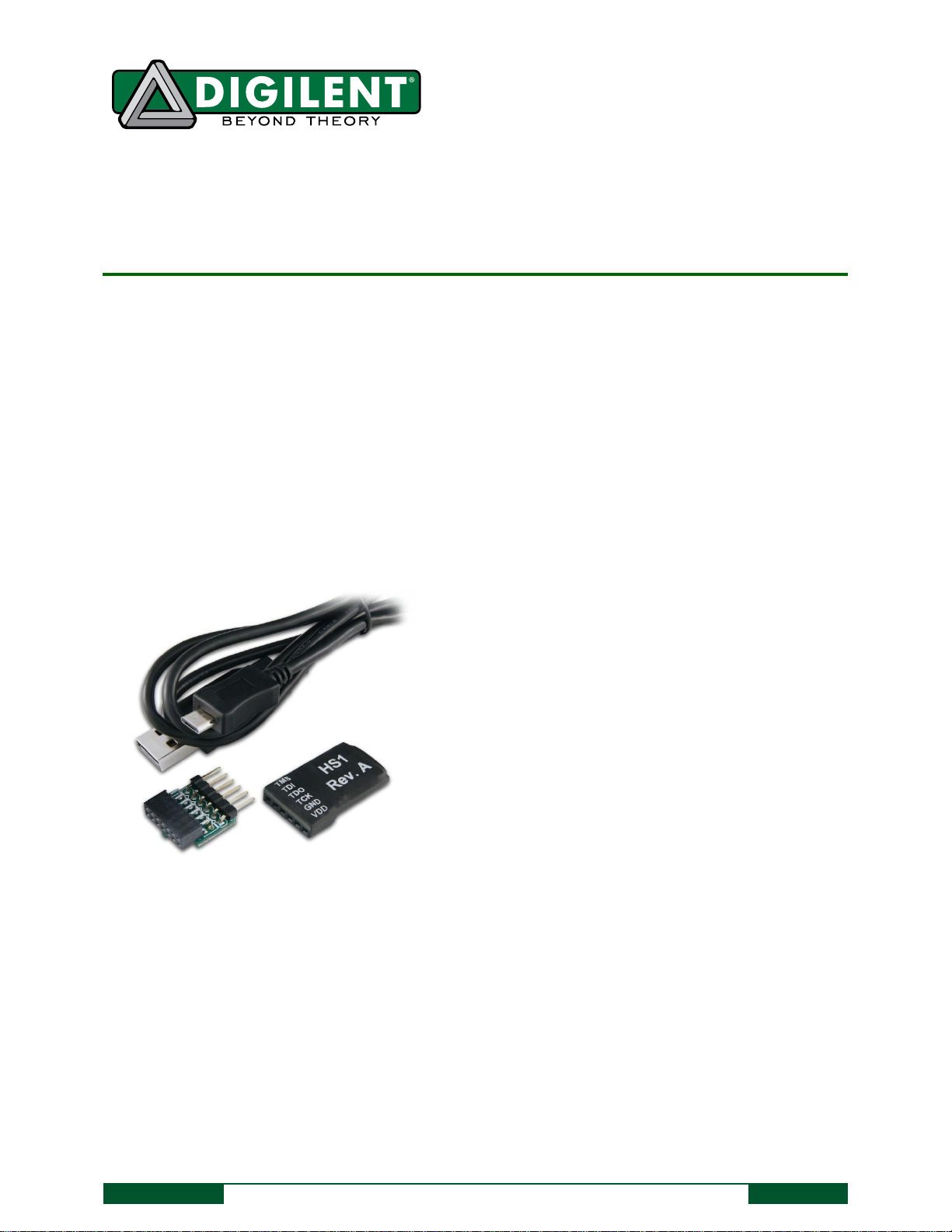
The JTAG-HS1.
Small, complete, all-in-one JTAG programming solution
for Xilinx FPGAs
Separate Vref drives JTAG/SPI signal voltages; Vref can
be any voltage between 1.8V and 5V.
High-Speed USB2 port that can drive JTAG/SPI bus at up
to 30Mbit/sec
JTAG/SPI frequency settable by user
Compatible with all Xilinx tools
Uses micro-AB USB2 connector
SPI programming solution (modes 0 and 2 supported)
Fully supported by the Adept SDK, allowing custom
JTAG/SPI applications to be created
Features include:
Overview
The joint test action group (JTAG)-HS1 programming cable is a high-speed programming solution for Xilinx fieldprogrammable gate arrays (FPGAs). It is fully compatible will all Xilinx tools, and can be seamlessly driven from
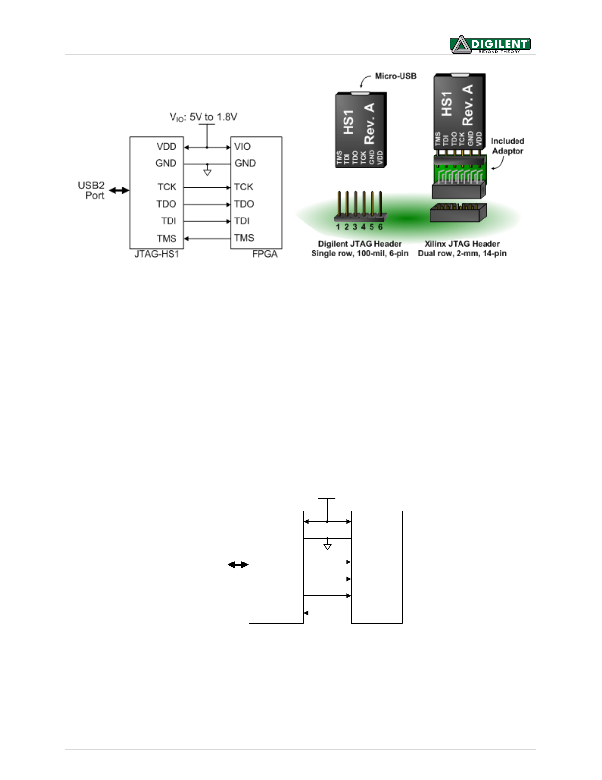
iMPACT, Chipscope™, and EDK. The HS1 attaches to target boards using Digilent's 6-pin, 100-mil spaced
programming header, or Xilinx's 2x7, 2mm connector (using the included adaptor).
The JTAG-HS1 is powered from a PC's USB port, and will be recognized as a Digilent programming cable when
connected to a PC, whether or not it is attached to the target board. A separate Vdd pin is provided on the HS1 to
supply JTAG signal buffers. The high speed, 24mA, three-state buffers allow target boards to drive the HS1 with
signal voltages from 1.8V to 5V, with bus speeds of up to 30MBit/sec. The HS1's Vdd pin must be tied to the same
voltage supply that drives the JTAG port on the FPGA (see Fig. 1).
JTAG signals are held in high-impedance except when actively driven during programming, so the JTAG bus can be
shared with other devices. The HS1 uses a standard Type-A to Micro-USB cable (included with the HS1) that
attaches to the end of the module opposite the system board connector. The HS1 is small and light, allowing it to
be held firmly in place by the system board connector (see Fig. 2).
Page 2
JTAG-HS1™ Programming Cable for Xilinx® FPGAs
Copyright Digilent, Inc. All rights reserved.
Other product and company names mentioned may be trademarks of their respective owners.
Page 2 of 4
VIO: 5V to 1.8V
USB2
Port
TMS
TDI
TDO
TCK
SS
MOSI
MISO
SCK
SPI DeviceJTAG-HS1
GND
VDD
GND
VIO
Figure 1. Diagram of signal voltages and connections.
Figure 2. Xilinx JTAG headers.
Figure 3. JTAG-HS1 SPI Device Connections.
Software Support
In addition to working seamlessly with all Xilinx tools, the HS1 is supported by Digilent's Adept software and the
Adept SDK (the SDK can be freely downloaded from Digilent's website). Adept includes a full-featured
programming environment, and a set of public APIs that allow user applications to directly drive the JTAG chain.
Using the Adept SDK, custom applications can be created to drive JTAG ports on virtually any device. The HS1 also
supports SPI modes 0 and 2. Users may utilize the APIs provided by the SDK to create applications that can drive
any SPI device supporting those modes. Please see the Adept SDK reference manual for more information.
The HS1 is also supported by Digilent's AVR programmer that can target any AVR device
Page 3

JTAG-HS1™ Programming Cable for Xilinx® FPGAs
Copyright Digilent, Inc. All rights reserved.
Other product and company names mentioned may be trademarks of their respective owners.
Page 3 of 4
Symbol
Parameter
Condition
Min
Max
Unit
Vdd
Operating supply voltage
-0.3
4.0
V
Vref
I/O reference/supply voltage
-0.3
6
V
VIO
Signal Voltage
-0.3
6
V
IIK,IOK
TMS, TCK, TDI, TDO
DC Input/Output Diode Current
VIO < -0.3V
-50
mA
VIO > 6V
+20
I
OUT
DC Output Current
±50
mA
T
STG
Storage Temperature
-20
+120
ºC
ESD
Human Body Model JESD22-A114
2000
V
Charge Device Model JESD22-C101
500
V
Symbol
Parameter
Min
Typ
Max
Unit
Vdd
Operating supply voltage
2.97
3.3
3.63
Volts
Vref
I/O reference/supply voltage
1.65
2.5/3.3
5.5
Volts
TDO
Input High Voltage (VIH)
0.75 x Vref
5.5
Volts
Input Low Voltage (VIL)
0
0.25 x Vref
Volts
TMS, TCK, TDI
Output High (VOH)
0.85 x Vdd
0.95 x Vdd
Vdd
Volts
Output Low (VOL)
0
0.05 x Vdd
0.15 x Vdd
Volts
Absolute Maximum Ratings
DC Operating Characteristics
Page 4

JTAG-HS1™ Programming Cable for Xilinx® FPGAs
Copyright Digilent, Inc. All rights reserved.
Other product and company names mentioned may be trademarks of their respective owners.
Page 4 of 4
Symbol
Parameter
Min
Max
TCK
TCK period
33ns
2.185ms
T
CKH
, T
CKL
T
CLK
pulse width
20ns
1.1ms
TCD
T
CLK
to TMS, TDI
0
15ns
TSU
TDO Setup time
19ns
THD
TDO Hold time
0
TMS/TDI
TCK
TDO
T
CKL
T
CKH
T
CK
T
CD
T
SU
T
HD
Figure 4. Timing diagram.
Table 1.Common frequencies.
AC Operating Characteristics
HS1 JTAG/SPI signals are driven according to the timing diagram below in Fig. 4. TCK frequencies from 30 MHz to 8
KHz are supported at integer divisions of 30 MHz from 1 to 3750. Common frequencies include 30 MHz, 15 MHz,
10 MHz, and 6 MHz (see Table 1).
Design Notes
The HS1 is designed to drive JTAG/SPI signals on target boards that have less than 100ohms of series resistance.
Higher resistance may result in degraded operation.
Supported Target Devices
The JTAG-HS1 is capable of targeting the following Xilinx devices:
1. Ordered List Item Xilinx FPGAs
2. Xilinx Zynq-7000
3. Xilinx CoolRunner™/CoolRunner-II CPLDs
4. Xilinx Platform Flash ISP configuration PROMs
5. Select third-party SPI PROMs
6. Select third-party BPI PROMs
The following devices cannot be targeted by the JTAG-HS1:
1. Ordered List ItemXilinx 9500/9500XL CPLDs
2. Xilinx 1700 and 18V00 ISP configuration PROMs
3. Xilinx FPGA eFUSE programming
Remote device configuration is not supported for the JTAG-HS1 when used with Xilinx's iMPACT software. Note:
Please see the "Introduction to Indirect Programming – SPI or BPI Flash Memory" help topic in iMPACT for a list of
supported FPGA/PROM combinations. Note: Please see the "Configuration Memory Support" section of Xilinx
UG908 for a list of the FPGA/PROM combinations that Vivado supports.
 Loading...