

Page 1
CCeerreebboott NNaannoo™
RReeffeerreennccee MMaannuuaal
Revision: February 6, 2009
Note: This document applies to REV A of the board.
™
l
Overview
The Cerebot Nano is the smallest in the
Cerebot line of boards offered by Digilent. The
board’s small size allows it to be used as either
a peripheral that can be plugged directly into
other Digilent boards or as a tiny stand-alone
embedded control board. In spite of its small
size, the Cerebot Nano is packed with
features.
The Cerebot Nano’s versatile design and
programmable microcontroller allows you to
control different external devices and program
the board for multiple uses. The board has
many I/O connectors and supports a number of
programming tools including Atmel AVR
Studio® 4 and WinAVR.
The Cerebot Nano has a number of
connections for peripheral devices. Digilent
peripheral modules (Pmods™) include Hbridges, analog-to-digital and digital-to-analog
converters, a speaker, switches, buttons,
LEDs, RS232 converters, screw terminal
connectors, BNC connectors, servo motors,
and more. For more information see
www.digilentinc.com.
Features include:
• ATmega168 microcontroller
• one 6-pin and two 12-pin connectors for
Digilent Pmod peripheral module
boards
• up to eight analog-to-digital (ADC) input
channels
• four LEDs
• ESD protection for all I/O pins
• in-system programming support using
the Digilent parallel JTAG cable or the
Digilent USB JTAG/SPI cable.
16K Flash
(Internal)
512 EEPROM
(Internal)
1K SRAM
(Internal)
www. d i g i l e n t i n c . c om
215 E Main Suite D | Pullman, WA 99163
(509) 334 6306 Voice and Fax
Power
connector
ATMega168
MLF32
Cerebot Nano
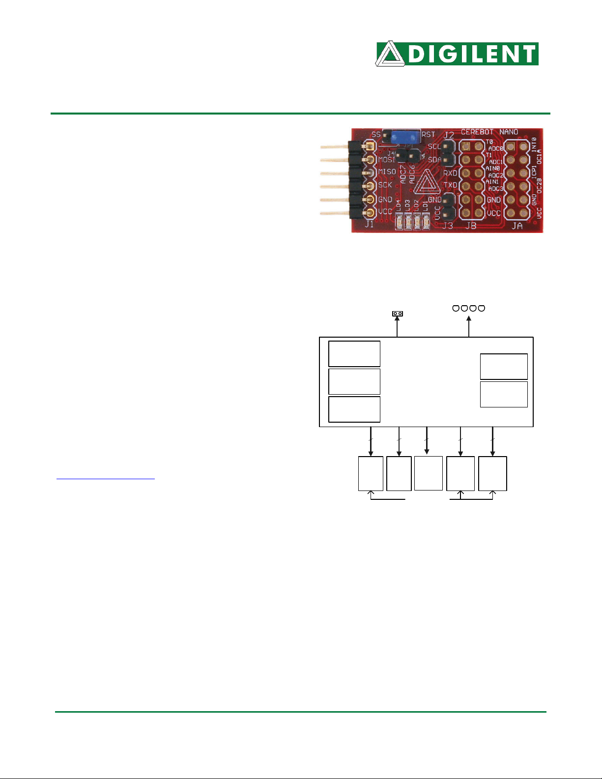
2
J1
SPI/
ISP
J2/
TWI
J4
ADC6/7
I/O Connectors
Cerebot Nano Circuit Diagram
4 LEDs
JA
ADCs/
IO
TM
12
USART/
Internal
Oscillator
UART, SPI,
& TWI ports
1226
JB
TWI/
IO
®
Doc: 502-095 page 1 of 6
Copyright Digilent, Inc. All rights reserved. Other product and company names mentioned may be trademarks of their respective owners.
Page 2

Cerebot Nano Reference Manual
Features of the ATmega168 include:
• master/slave serial peripheral interface
(SPI)
• programmable serial USART interface
• Atmel two wire serial interface (TWI)
• eight channel, 10-bit ADC
• two 8-bit timer/counters
• one 16-bit timer/counter
• 16KB program flash
• 512 byte EEPROM
• 1KB internal SRAM
• analog comparator
• built-in 8MHz/1MHz clock source.
For more information on the ATmega168
microcontroller, refer to the data sheet
available at www.atmel.com.
Functional Description
The Cerebot Nano is designed for embedded
control and robotic applications as well as
microprocessor experimentation. Embedded
firmware, suitable for many applications, can
be programmed into the Cerebot Nano’s
ATmega168 microcontroller.
Although the Cerebot Nano can be used as a
stand-alone microcontroller board, it is also
designed to be part of a larger system using a
distributed processing architecture. Connector
J1 allows the Cerebot Nano to be plugged
directly into other Digilent microcontroller
boards, such as the Cerebot II or Cerebot Plus.
The Cerebot Nano can be plugged directly into
ports on many of Digilent’s FPGA boards,
although some boards may require the use of
the Digilent Module Interface Board.
The Cerebot Nano can be programmed with
firmware to perform local control functions. It
can then be controlled by, and report back to, a
higher level controller in the host controller
board. For example, the Cerebot Nano could
be programmed to perform closed-loop motor
speed control. It could relieve extra work for
the host processor, when performing the motor
Digilent, Inc.
speed control, by processing commands from
the host and controlling the motors itself.
Communication Options
Connector J1 provides access to the
master/slave SPI. SPI is a high-speed,
synchronous, serial interface used by many
serial peripheral devices like ADCs and DACs.
The SPI interface is used for programming the
ATmega168 and as a user-accessible SPI
port. The Digilent PmodAD1 and PmodDA1
modules use the SPI interface.
Connectors JB and J2 provide access to the
Atmel two-wire interface (TWI). The TWI is a
medium speed (200-400 Kbps) serial bus that
allows up to 128 devices to be connected.
Connector J2 can be used to daisy chain other
devices to the TWI bus. Atmel’s TWI interface
is directly compatible with Phillips’ I2C protocol.
The ATmega168 microcontroller provides a
USART that can be used for asynchronous or
synchronous serial communications. However,
the Cerebot Nano doesn’t provide for a crystal
oscillator, and the internal RC oscillator isn’t
accurate enough for reliable asynchronous
communications. It is sometimes possible to
tune the oscillator using the calibration register
to allow asynchronous communications to
work.
www.digilentinc.com page 2 of 6
Copyright Digilent, Inc. All rights reserved. Other product and company names mentioned may be trademarks of their respective owners.
Page 3

Cerebot Nano Reference Manual
6-Pin Pmod Headers
The Cerebot Nano has five 6-pin header
connectors for connecting to general-purpose,
off-board digital I/O or to specific ATmega168
features like analog-to-digital converters or
pulse-width modulators. Each 6-pin connector
provides four signals, power, and ground.
These connectors are specifically designed to
work with the Digilent Pmod line of peripheral
boards, but can be used to connect to virtually
any off-board I/O device.
See Table 1 for more information on
connecting peripheral modules and other
devices to the Cerebot Nano. Table 1 shows
the connectors with their designed base
function and a map to the ATmega168 I/O
ports. All I/O port signal pins can be used for
general-purpose digital I/Os.
Power Supply
The Cerebot Nano is rated for external power
ranging from 2.7 to 5.5 volts DC. The Cerebot
Nano does not feature a voltage regulator, so
care should be exercised when selecting a
power source. Using voltage outside this
range could damage the Cerebot Nano and
connected devices.
The Cerebot Nano can be powered through
any of the board’s 6-pin Pmod headers or the
J3 connector.
Each of these connectors provides a VCC and
a ground pin. A power supply providing
between 2.7 and 5.5 volts can be connected to
the VCC pin on any one of these connectors.
When the Cerebot Nano is plugged into
another Digilent microcontroller or FPGA
board, that board can power the Cerebot Nano
through the Pmod connector. The host board
should be jumpered to provide 3.3V on the
VCC pin of the Pmod connector being used.
The Cerebot Nano will then be powered by the
host board’s power supply, and will in turn
provide power from the host board to any
For standalone applications, the Digilent
PmodREG1 voltage regulator module can be
used to supply 3.3 volts to the board.
Device Programming
The Cerebot Nano has one in-systemprogramming (ISP) connector, J1. A Digilent
programming cable is connected to J1. Either
a parallel JTAG or USB JTAG/SPI cable can
be used. When connecting the programming
cable, ensure that the VCC and GND pin
labels from the cable match to the VCC and
GND pins on the Cerebot Nano.
A power supply must be provided to the
Cerebot Nano when programming. The
Digilent programming cable does not supply
power to the board; the board that it is plugged
into powers the programming cable. The
Digilent PmodREG1 voltage regulator module
can be used, or any appropriately regulated
power supply can be connected to J3. If the
Cerebot Nano is being used in conjunction with
another Digilent board, such as the Cerebot II
or Minicon, these boards have connectors that
can be used to supply power to the J3
connector on the Cerebot Nano using a twowire cable.
Programming can be accomplished using the
Digilent AVRP application, available by free
download from the Digilent web site. It is also
possible to configure the AVRDUDE
programmer in the WinAVR release for insystem-programming using the Digilent parallel
JTAG cable. See the documentation for these
applications for more information on board
programming.
Connector J1 is used both for in-systemprogramming and for user access to the SPI
controller. The jumper block JP1 is used to
select between the two functions. The shorting
block is placed in the RST position for insystem-programming, and in the SS position
for user access to the SPI port.
Digilent, Inc.
peripheral boards connected to the Cerebot
Nano’s other Pmod connectors.
www.digilentinc.com page 3 of 6
Copyright Digilent, Inc. All rights reserved. Other product and company names mentioned may be trademarks of their respective owners.
Page 4

Cerebot Nano Reference Manual
AVR Clock Fuse Settings
AVR microcontrollers use control bits called
fuses to set basic operating parameters for the
device. The SPI controller uses the clock
source set by the fuses for its clock. If the clock
source fuses are set to select a clock source
that doesn’t exist on the board, the SPI
controller won’t work and it will no longer be
possible to program the microcontroller via the
in-system programming protocol. The Cerebot
Nano can only use the internal RC oscillator as
the clock source.
If the external oscillator, or one of the
crystal/resonator clock sources is selected, it
may be possible to recover the board by
applying a suitable clock signal to pin 1 of
connector JB. There is an applications note on
the Digilent web site illustrating this technique
for the Cerebot board.
In addition, the maximum SPI clock frequency
is the selected clock frequency divided by four.
If the 128KHz internal oscillator is selected as
the clock source, the SPI clock would need to
be set to a frequency of 32KHz or less. The
Digilent programming cables do not support
frequencies that low, so if the 128KHz internal
oscillator is selected for the clock source, the
board will no longer be programmable using
the Digilent programming cable.
Two-Wire Serial Interface
The Atmel TWI interface is a medium speed
(400 Kbps), synchronous, serial,
communications bus. The TWI interface
Pins one and two of connector JB and
connector J2 provide two positions for
connecting to the TWI signals. By using twowire cables (available separately from
Digilent), a daisy chain of Cerebot Nanos or
other TWI-capable boards can be created.
The TWI bus is an open-collector bus. Devices
on the bus actively drive the signals low. When
no device is driving the lines low, pull-up
resistors achieve the high state on the TWI
lines. A single device on the TWI bus must
provide the pull-up resistors.
The Cerebot Nano provides pull-up resistors
that are controlled by software.
I/O port B, bits 6 and 7 (PB6 and PB7), are
connected to the pull-up resistors. To enable
the pull-ups, configure these pins as outputs
and set the I/O port output bits to “1”. To
disable the pull-ups, configure these pins as
inputs with the internal pull-ups disabled. Both
TWI pull-ups should be enabled or disabled
together. Only one device on the TWI bus
should have pull-ups enabled.
A port bit is configured as an input or an output
by setting the corresponding bit in the DDR
register. The pin becomes an output by writing
a “1” and an input by writing a “0”. When a pin
is configured as an input, an internal pull-up
resistor is enabled by writing the corresponding
output port bit to “1” and disabled by writing it
to “0”. See the Atmel Atmega168 data sheet
for more information.
Digilent, Inc.
supports master or slave operation with up to
128 devices on the bus. Each device is given a
unique address, and the protocol has the
ability to address packets to a specific device
or to broadcast packets to all devices on the
bus. For detailed information on configuring
and using the two-wire interface see the
ATmega168 data sheet at www.atmel.com.
The Cerebot Nano has two ways to connect to
a TWI bus. The TWI signals, SCL and SDA,
are available on 6-pin connector JB or on the
2-pin connector J2.
www.digilentinc.com page 4 of 6
Copyright Digilent, Inc. All rights reserved. Other product and company names mentioned may be trademarks of their respective owners.
Page 5

Cerebot Nano Reference Manual
On-Board User I/O
The Cerebot Nano provides four on-board
LEDs for user output. The LEDs are connected
to I/O Port D, bits 2-5 (PD2-PD5). An LED is
turned on by writing the corresponding DDRD
and PORTD register bits to logic 1 and turned
off by writing the corresponding PORTD bit to
logic 0.
The LED connections are shared with ports JA
and JB as follows:
LED1 JB8 PD5
LED2 JA10 PD3
LED3 JB7 PD4
LED4 JA7 PD2
Digilent, Inc.
www.digilentinc.com page 5 of 6
Copyright Digilent, Inc. All rights reserved. Other product and company names mentioned may be trademarks of their respective owners.
Page 6

Cerebot Nano Reference Manual
Digilent, Inc.
All Pmod connector pins can be used for general purpose I/Os. The following table describes how the
Cerebot Nano header pins connect to ATmega168 ports/bits.
JA Analog Input and PmodHB5 Connections
JB Serial Communication and General I/O
J1 SPI Interface and In-System Programming
J2 TWI Connectors
J4 ADC Input Only
DESCRIPTION PIN FUNCTION PORT/BIT
JA1 through JA4 can be used as analog inputs in
applications and pins JA7 through JA10 are ideally suited
for connection with a Digilent PmodHB5 motor control
board.
Pins JB1 through JB4 provide access to the TWI and
USART communication interfaces. Pins JB7 and JB10 are
limited to general I/O and JB8 and JB9 provide access to
the output compare pins of Timer/Counter 0.
When the shorting block on JP1 is in the SS position, J1 is
used for the SPI port. When the shorting block on JP1 is in
the RST position, J1 is used for in-system programming.
The Atmel TWI interface can be accessed on this
connector.
Analog to digital input channels 6 and 7 are input-only and
have digital I/O capabilities.
1 ADC0/PCINT8 PC0
2 ADC1/PCINT9 PC1
3 ADC2/PCINT10 PC2
4 ADC3/PCINT11 PC3
5 GND
6 VCC
7 INT0/PCINT18 PD2
8 OC1A/PCINT1 PB1
9 ICP1/PCINT0 PB0
10 INT1/PCINT19 PD3
11 GND
12 VCC
1 ADC5/SCL/PCIN
T13
2 ADC4/SDA/PCIN
T12
3 RXD/PCINT16 PD0
4 TXD/PCINT17 PD1
5 GND
6 VCC
7 XCK/T0/PCINT20 PD4
8 T1/OC0B/PCINT
21
9 AIN0/OC0A/PCIN
T22
10 AIN1/PCINT23 PD7
11 GND
12 VCC
1 PCINT2/SS/OC1B PB2
2 PCINT3/OC2A/M
OSI
3 PCINT4/MISO PB4
4 SCK/PCINT5 PB5
5 GND
6 VCC
1 ADC5/SCL/PCIN
T13
2 ADC4/SDA/PCIN
T12
1 ADC6
2 ADC7
PC5
PC4
PD5
PD6
PB3
PC5
PC4
www.digilentinc.com page 6 of 6
Copyright Digilent, Inc. All rights reserved. Other product and company names mentioned may be trademarks of their respective owners.
 Loading...