

Page 1
DDiiggiilleenntt PPmmooddOODD11™™ OOppeenn DDrraaiinn
®
OOuuttppuutt MMoodduullee BBooaarrdd RReeffeerreennccee
MMaannuuaal
Revision: February 23, 2007
Note: This document applies to REV A of the board.
Overview
The Digilent PmodOD1 Open Drain Output
Module Board (PmodOD1) can drive high
current devices using On-Semiconductor
NTHD4508NT power FET output transistors.
The output transistors are driven by logic
signals from a Digilent system board.
The output transistors function as low side
switches, sinking current from an external
voltage source to ground. The outputs can be
used to drive DC motors, stepper motors,
relays, solenoids or other electrical devices
operated via a switch closure to ground.
Flyback protection diodes are included on each
output to allow the outputs to drive inductive
loads.
Features include:
• two NTHD4508 dual power FETs
• 4.1A peak output current (t < 5s)
• 3.0A continuous current (at 25°C), 2.2A
• a 6-pin header for inputs
• two screw terminal blocks for outputs
• 20V max. output voltage
• small form factor (0.80” x 1.15”).
Functional Description
The PmodOD1 module is designed to work
with either Digilent programmable logic system
boards or embedded control boards. Most
Digilent system boards, like the Basys, Nexys
or Cerebot , have 6-pin connectors that allow
the PmodOD1 to plug directly into the system
board or to connect via a Digilent 6-pin cable.
Some older Digilent boards may need a
Digilent Module Interface Board (MIB) and a 6pin cable to connect to the PmodOD1.
l
continuous current (at 85°C)
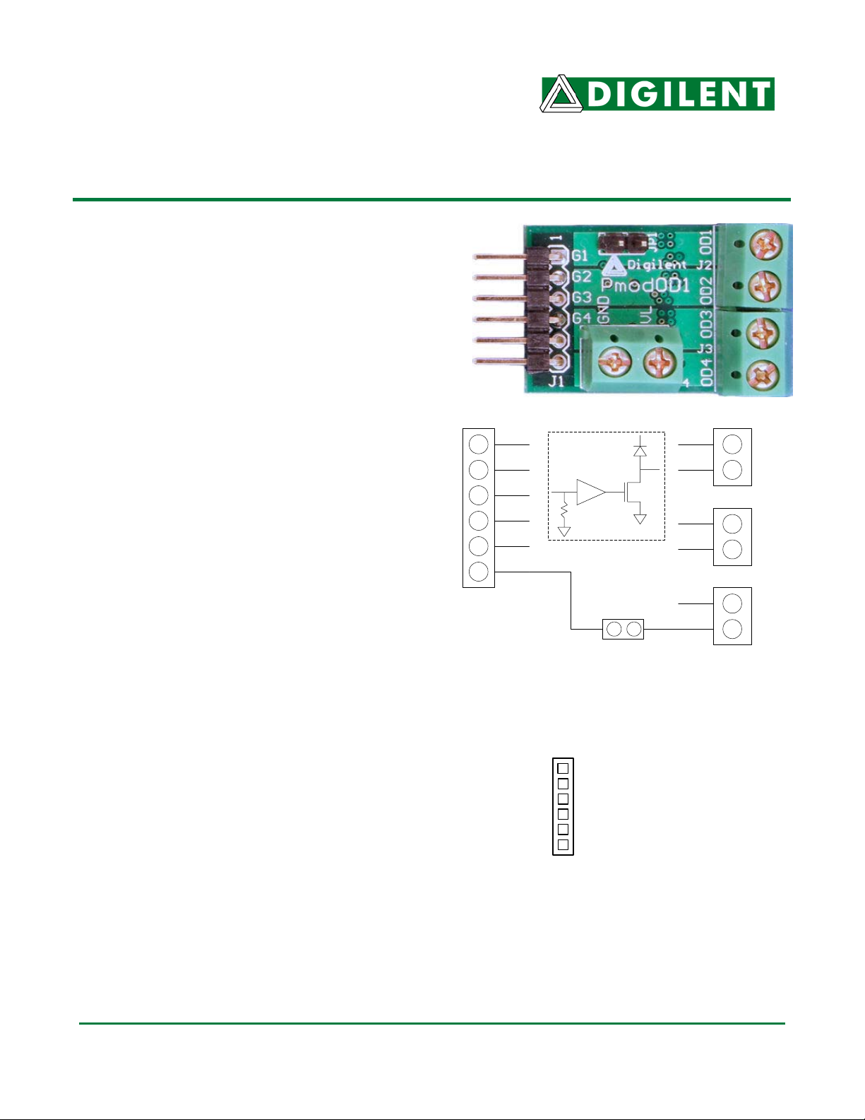
The
G1
G2
G3
G4
GND
Vcc
J1
MIB plugs into the system board and the cable
connects the MIB to the PmodOD1.
Figure 2 PmodOD1 Input Connector, J1
The PmodOD1 provides four logic level inputs,
G1-G4. Each input connects to a Schmitt
trigger, non-inverting buffer that drives the gate
of the corresponding output transistor. Driving
an input high will drive
corresponding output transistor high,
www.digilentinc.com
215 E Main Suite D | Pullman, WA 99163
(509) 334 6306 Voice and Fax
Typical Circuit (4x)
OD
OD1
OD2
OD3
OD4
GND
VL
VL
JP1
Figure 1 PmodOD1 Block Diagram
(1) G1
(2) G2
(3) G3
(4) G4
(5) GND
(6) Vcc (3.3 - 5V)
the gate of the
J2
J3
J4
Doc: 502-125 page 1 of 2
Copyright Digilent, Inc. All rights reserved. Other product and company names mentioned may be trademarks of their respective owners.
Page 2
PmodOD1 Reference Manual Digilent Confidential Digilent, Inc.
turning the transistor on. The output transistor
will then sink current to ground. Driving an
input low drives the gate of the transistor low,
turning off the output transistor. Each input has
a pull-down resistor that prevents the output
from turning on unless it is actively being
driven high.
Access to the outputs of the PmodOD1 is
provided by screw terminal blocks J2 and J3.
The outputs are labeled OD1 – OD4. Input G1
controls output OD1 and so on. Each output is
connected to the drain of the corresponding
output transistor and functions like a low
impedance switch closure to ground.
Each output provides a clamp diode to prevent
damage due to flyback voltages generated by
inductive loads. Each output transistor
functions independently of the others, so they
can be used individually or simultaneously.
VL
GND
Clamp
Diode
ODn
Output
Transistor
Figure 3 Output Circuit with Load Connection
External Ground
J4
J2
or
J3
External Voltage
External
Load
As illustrated in Figure 3, a load is connected
so that current from an external voltage source
conducts through the load to ground when the
output transistor is turned on. In order to
complete the circuit, the GND pin on J4 must
be connected to the ground for the external
voltage supply. Additionally, the external
voltage source must be connected to the VL
pin on J4 to complete the circuit for the output
clamp diode.
For more information, the PmodOD1
schematic is available at
www.digilentinc.com.
www.digilentinc.com Copyright Digilent, Inc. Page 2
 Loading...