

Page 1

PPmmooddJJSSTTKK™
RReeffeerreennccee MMaannuuaal
Revision: September 22, 2008
Note: This document applies to REV C of the board.
™
l
Overview
The PmodJSTK was designed to be a versatile
user interface that can be used in a wide
variety of projects. It contains a resistive twin
axis joystick that includes a center push button
along with two additional push buttons. Also,
PmodJSTK has two programmable LEDs
located on the board that can provide
additional information to the user.
The PmodJSTK is ideally suited for Digilent
microcontroller or FPGA based projects that
required proportional control from the user,
such as robotic applications.
Functional Description
The joystick, located on the PmodJSTK,
contains two potentiometers which are
manipulated by moving the joystick in the X
and Y directions.
The PmodJSTK is equipped with an embedded
Atmel® ATtiny24 microcontroller in a MLF20
package. This microcontroller utilizes an
analog to digital converter to measure the
voltage occurring on the sweeper pins of each
of the two potentiometers. The voltage
occurring at these sweeper pins ranges from
ground potential to VCC depending on the
position of the joystick. A button is also
attached to the joystick and is activated by
pressing down directly on the joystick. The
joystick’s center button, along with the two
additional push buttons, is read by the
microcontroller.
The microcontroller assembles the joystick’s
positional data, along with the status of the
push buttons, in a series of five bytes. It
provides a 10-bit value for each axis of the
joystick. The joystick’s axis values are each
placed in 16-bit values, which are made up of
an upper byte and a lower byte.
www. d i g i l e n t i n c . c om
215 E Main Suite D | Pullman, WA 99163
(509) 334 6306 Voice and Fax
Figure 1 PmodJSTK Circuit Diagram
Figure 2 Joystick Axis Map
®
Doc: 502-116 page 1 of 3
Copyright Digilent, Inc. All rights reserved. Other product and company names mentioned may be trademarks of their respective owners.
Page 2
PmodJSTK Reference Manual
The two least significant bits of the upper byte,
along with the entire lower byte, make up the
10-bit value that was calculated.
By referring to the Joystick Axis Map located
above, it is possible to know what X and Y
values to expect from the PmodJSTK, based
on the current position of the joystick.
The X and Y position data make up the first
four bytes of the five byte series. The last byte
contains the positions of the three buttons,
indicated by the three least significant bits in
the byte.
Communication
of these bytes is shifted in, the master will have
received a byte of data from the PmodJSTK.
The two programmable LEDs located on the
PmodJSTK are turned on or off based on the
status of the first of the five bytes shifted into
the PmodJSTK. The two least significant bits
of the first byte determine the status of the
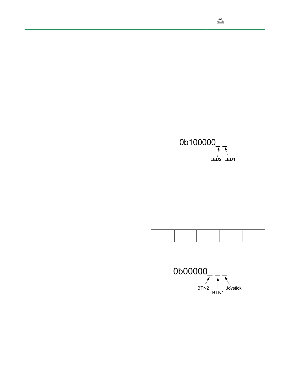
LEDs. For example, if the first byte shifted into
the PmodJSTK is 0b00 (0x00), then both LEDs
will be off. If the first byte is 0b01 (0x01), only
LED1 will be on and similarly if 0b10 (0x02) is
shifted in, then only LED2 will be on. Both will
be turned on if 0b11 (0x03) is shifted in as the
first byte. Write to the LEDs using the
following format:
Digilent, Inc.
The serial peripheral interface (SPI) mode 0
method of communication is used to
communicate between the PmodJSTK and the
master board
To receive data from the PmodJSTK using
SPI, a byte must be shifted into the
PmodJSTK. As the byte is shifted into the
PmodJSTK, it shifts out a data byte to the
master. This communication is accomplished
via the master-in slave-out (MISO) and masterout slave-in (MOSI) lines of the communication
bus. This communication must be
synchronously clocked using the serial clock
(SCK) line of the communication bus.
The PmodJSTK is enabled on the SPI bus by
lowering the slave select (SS) pin. The SS pin
is active low. The maximum recommended
SPI clock speed is 1 MHz. The minimum
recommended amount of time between the SS
Figure 3 LED Command
The remaining four bytes that are shifted in are
ignored by the PmodJSTK. After each byte
has been completely shifted in, the PmodJSTK
will have finished shifting out a byte of data to
the master.
The order of the bytes being transferred from
the PmodJSTK to the master is as follows:
1 2 3 4 5
X (low) X(high) Y (low) Y(high) Buttons
The buttons are reported in the last byte in the
following format:
pin going low and the start of data transmission
on the bus is 15µs. The minimum
recommended amount of time between the
end of one byte being shifted and the
beginning of the next is 10µs. The SS pin
should be returned high after communication
has been completed.
After lowering the SS pin, the master should
shift 5 bytes to the PmodJSTK in order to
receive data from the PmodJSTK. After each
Figure 4 Byte 5
A bit written to a ‘1’ indicates that the
corresponding button is being depressed, and
a ‘0’ indicates that it is not being depressed.
www.digilentinc.com Copyright Digilent, Inc. page 2 of 3
Page 3

PmodJSTK Reference Manual
Header Description Pin Function Ports
J1 SPI and 1 SS PA7
in-system 2 MOSI PA6
programming 3 MISO PA5
4 SCK PA4
5 GND
6 VCC
Figure 5 Header Pins to ATtiny24 Ports/Bit
Digilent, Inc.
www.digilentinc.com Copyright Digilent, Inc. page 3 of 3
 Loading...