

Page 1
DDiiggiilleenntt PPmmooddDDAA22™™ DDiiggiittaall TToo
®
AAnnaalloogg MMoodduullee CCoonnvveerrtte
RReeffeerreennccee MMaannuuaall
Revision: September 25, 2006
err BBooaarrdd
www.digilentinc.com
215 E Main Suite D | Pullman, WA 99163
(509) 334 6306 Voice and Fax
Overview
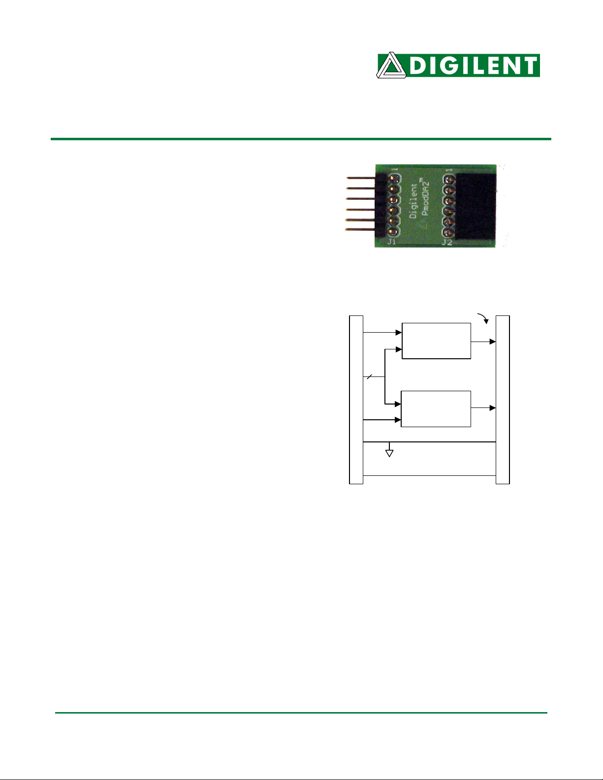
The Digilent PmodDA2 Digital to Analog
Module Converter, converts signals from digital
values to analog voltages on two channels
simultaneously with twelve bits of resolution.
The PmodDA2 uses a 6-pin header connector
and, at less than one square inch, is small
enough to be located where the reconstructed
signal is required.
Features include:
• two National Semiconductor
DAC121S101, 12-bit D/A converters
• a 6-pin header and 6-pin connector
• two simultaneous D/A conversion
channels
• very low power cons um ption
• small form factor (0.80” x 0.80”).
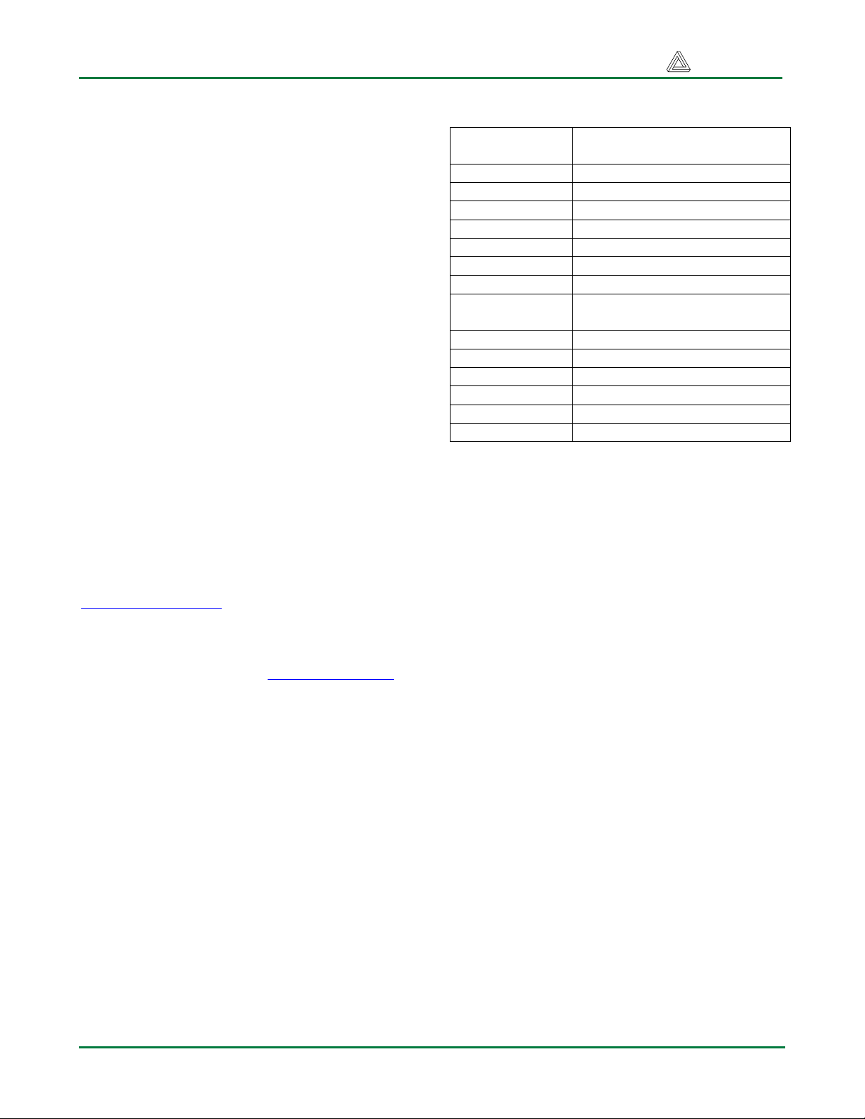
Functional Description
The PmodDA2 can produce an analog output
ranging from 0-3.3 volts when operated with a
3.3V power supply. It has two simultaneous
D/A conversion channels, each with a 12-bit
converter that can proc ess s e p ar at e d i git a l
signals.
The PmodDA2 is equipped with two
DAC121S101 digital to analog converters.
Sending commands via the
SPI/MICROWIRE™ serial bus to the D/A
converters produces outputs. The two
converters are conn e cted in parallel so that
commands are sent to both converters
simultaneously.
The PmodDA2 is designed to work with either
Digilent programmable logic system boards or
embedded control system boards. Most
Digilent system boards, such as the Nexys,
Basys, or Cerebot, have 6-pin
Doc: 502-113 page 1 of 2
Copyright Digilent, Inc. All rights reserved. Other product and company names mentioned may be trademarks of their respective owners.
connectors that allow the PmodDA2 to plug
directly into the system board or to connect via
a Digilent six-wire cable
Some older Digilent boards may need a
Digilent Module Interface Board (MIB) and a 6pin cable to connect to the PmodDA2. The MIB
plugs into the system board and the cable
connects the MIB to the PmodDA2.
Digilent PmodDA2
D1
Sync,
2
Clock
D2
J1 Connector
GND
VCC
Block Diagram
Figure 1
Analog Output s
DAC121S101
D/A
Conv erter
DAC121S101
D/A
Conv erter
Figure 2
J2 Connector
Page 2
Document Title Digilent Confidential Digilent, Inc.
See Table 1 for a description of the signals on
the interface connectors J1 and J2. For
additional information, refer to the PmodDA2
schematic available on the Digilent web site at
www.digilentinc.com.
The PmodDA2 is usually powered from the
Digilent system board connected to it. The
power and ground connections are on pins five
and six of the digital interface connector J1.
Alternatively, the PmodDA2 can be p owered
from an external power supply provided
through pins five and six of the analog
interface connector J2. In this case the power
select jumper on the system board should be
set to disconnect power from the system board
to J1. Damage may result if two power
supplies are connected at the same time.
The Digilent convention is to provide 3.3V to
power Pmod modules. The Pm odD A 2 c an b e
operated at any power supply voltage between
2.7V and 5.5V, however caution should be
exercised if using any voltage greater than
3.3V, as damage to the Digilent system board
could result. For more information refer to
reference manuals or schematics for the
system board available at
www.digilentinc.com
.
For detailed information about the National
Semiconductor data sheet refer to the National
Semiconductor web site at www.national.com
.
Table 1: Interface Connector Signal
Descriptions
Digital
Interface – J1
1 SYNC (common)
2 DINA (converter IC1)
3 DINB (converter IC2)
4 SCLK (common)
5 GND
6 VCC
Analog
Interface – J2
1 VOUTA (converter IC1)
2 N/C
3 VOUTB (converter IC2)
4 N/C
5 GND
6 VCC
www.digilentinc.com Copyright Digilent, Inc. Page 2
 Loading...