

Page 1
CCeerreebboott 3322MMXX77™
RReeffeerreennccee MMaannuuaal
Cerebot 32MX7 Circuit Diagram
Revision: October 20, 2011
Note: This document applies to REV C of the board.
™ BBooaarrdd
l
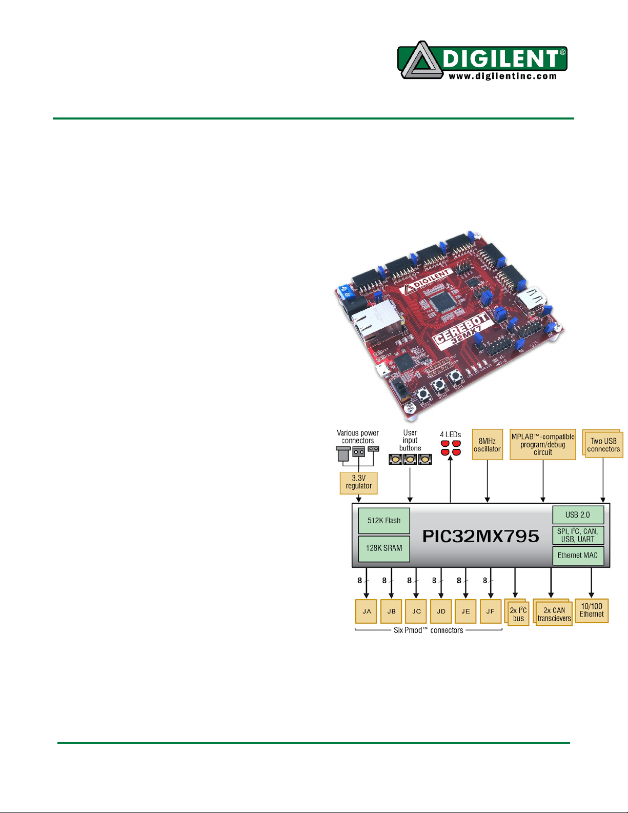
Overview
The Cerebot 32MX7 board is a useful tool for
embedded control and network
communications projects for both students and
hobbyists.
Its versatile design and programmable
microcontroller lets you access numerous
peripheral devices and program the board for
multiple uses. The board has many I/O
connectors and power supply options. It’s
network and communications features include
10/100 Ethernet interface, Full Speed USB 2.0
OTG interface, dual CAN network interfaces,
dual I2C buses, up to three UART ports and up
to three SPI ports.
The Cerebot 32MX7 works with the Microchip
MPLAB development environment and
provides built in programming and debugging
support within MPLAB.
The Cerebot 32MX7 provides a number of
connections for peripheral devices. It has six
connectors for attaching Digilent Pmod™
peripheral modules. Digilent Pmod peripheral
modules include H-bridges, analog-to-digital
and digital-to-analog converters, a speaker
amplifier, switches, buttons, LEDs, as well as
converters for easy connection to RS232,
screw terminals, BNC jacks, servo motors, and
more.
Features include:
• a PIC32MX795F512L microcontroller
• support for programming and
debugging within the Microchip MPLAB
development environment
• six Pmod connectors for Digilent
peripheral module boards
• 10/100 Ethernet
• USB 2.0 Device, Host, and OTG
support
• two CAN network interfaces
1300 Henley Court | Pullman, WA 99163
(509) 334 6306 Voice and Fax
• three push buttons
• four LEDs
• multiple power supply options, including
USB powered
• ESD protection and short circuit
protection for all I/O pins.
Doc: 502-186 page 1 of 19
Copyright Digilent, Inc. All rights reserved. Other product and company names mentioned may be trademarks of their respective owners.
Page 2

Cerebot 32MX7 Reference Manual
Features of the PIC32MX795F512L include:
• 512KB internal program flash memory
• 128KB internal SRAM memory
• USB 2.0 compliant full-speed On-The-
Go (OTG) controller with dedicated
DMA channel
• 10/100 Ethernet controller
• two CAN network controllers
• up to four serial peripheral interfaces
(SPI)
• up to six UART serial interfaces
• up to four I2C serial interfaces
• five 16-bit timer/counters
• five timer capture inputs
• five compare/PWM outputs
• sixteen 10-bit analog inputs
• two analog comparators
For more information on the
PIC32MX795F512L microcontroller, refer to
the PIC32MX5XX/6XX/7XX Family Data Sheet
and the PIC32 Family Reference Manual
available at www.microchip.com.
Functional Description
The Cerebot 32MX7 is designed for embedded
control and network communications
applications as well as general microprocessor
experimentation. Firmware suitable for many
applications can be downloaded to the Cerebot
32MX7’s programmable PIC32 microcontroller.
The board has a number of input/output
connection options, and is specially designed
to work with the Digilent line of Pmod
peripheral modules with various input and
output functions. For more information, see
www.digilentinc.com. In addition to the Pmod
connectors, the board provides three push
buttons and four LEDs for user i/o, as well as
providing connections for two I2C busses. A
serial EEPROM is provided on one of the I2C
busses.
The Cerebot 32MX7 can be used with the
Microchip MPLAB development environment.
In-system-programming and debug of firmware
www.digilentinc.com page 2 of 19
Copyright Digilent, Inc. All rights reserved. Other product and company names mentioned may be trademarks of their respective owners.
running on the PIC32MX795 microcontroller is
supported using an on-board program/debug
circuit licensed from Microchip.
The Cerebot 32MX7 features a flexible power
supply system with a number of options for
powering the board as well as powering
peripheral devices connected to the board. It
can be USB powered via either the debug USB
port or the USB device port, or it can be
powered from an external power supply or
batteries.
Programming and In-System
Debugging Using the MPLAB® IDE
The Cerebot 32MX7 board is intended to be
used with the Microchip MPLAB® IDE for
firmware development, programming and insystem debugging using a circuit licensed from
Microchip. MPLAB version 8.63 or later is
required for use of the on-board
program/debug circuit. The licensed debugger
is accessed via USB, using connector J15.
This connector is a micro-USB connector on
the lower left side of the board, near the power
switch. The provided USB cable should be
connected from J15 to a USB port on the
development PC for access to the board.
When creating a new project, use the
Configure.Select Device menu to specify the
PIC32 device in use. Ensure that the device is
set to PIC32MX795F512L.
To use the on-board program/debug circuit it
must be selected as the debugger or
programmer within the MPLAB IDE. Use the
Debugger.Select Tool menu, or the
Programmer.Select Tool menu, and select
“Licensed Debugger” as the programmer or
debugger.
The in-system programming/debugging
interface uses two pins on the PIC32
microcontroller. The PIC32 devices support
two alternate pin pairs for this interface:
PGC1/PGD1 or PGC2/PGD2. PIC32 devices
use PGC2/PGD2 by default. Due to conflicting
uses of the microcontroller pins, the Cerebot
Page 3

Cerebot 32MX7 Reference Manual
32MX7 is designed to use PGC1/PGD1.
Because of this, it is necessary to select the
use of PGC1/PGD1 for the debugging
interface. This is done using configuration
variables set using the
#pragma config
statement. The following statement must be
used to configure the microcontroller for use
with the on-board licensed debugger circuit:
#pragma config ICESEL = ICS_PGx1
The MPLAB IDE may report an error indicating
that the device is not configured for debugging
until a program containing this statement has
been programmed into the board.
Board Power Supply
Switch SW1, in the lower left corner of the
board is the power switch. Place this switch in
the ON position to turn on board power and in
the OFF position to turn off board power.
There are three power options for main power
to the board: USB powered from the debug
USB connector, USB powered from the USB
device connector, or external, non-USB
powered. Jumper block J16, (above the
Ethernet connector, J11) is used to select the
main power source. To select USB powered
from the debug connector, place the shorting
block in the DBG position. To select USB
power from the USB device connector, place
the shorting block in the USB position. This
option is used when the board is being used to
implement a bus powered USB device. To
power the board from an external power
supply, place the shorting block in the EXT
position. The board comes from the factor
jumpered for USB power from the debug USB
connector.
When powering the board from an external
power supply, there are two power supply
connectors that can be used: J17 and J18.
The barrel connector, J17, is used to power the
board from a “wall wart” style power supply.
This type of power supply is available from
many sources. Digilent has an optional power
Supply, that can be used with connector J17.
Connector J17 is a 2.5mm x 5.5mm coaxial
connector wired with the center terminal as the
positive voltage.
Connector J18 is a screw terminal connector
for an alternative power supply connection for
use with battery packs, bench supplies or other
power sources where use of a hard wired
power supply is desirable.
The Cerebot 32MX7 is rated for external power
from 3.6 to 5.5 volts DC. Using a voltage
outside this range will damage the board and
connected devices. For most purposes, when
using external power, a regulated 5V supply
should be used. When operating the board
from an external supply with a voltage less
than 5V, some features of the board won’t
work correctly.
When the Cerebot 32MX7 is operating as a
USB host, an external power supply connected
to either J17 or J18 must be used to power the
board. In addition to powering the logic on the
Cerebot 32MX7 board, this supply provides the
USB bus voltage supplied to any connected
USB device and must be a regulated 5V with
at least 500mA current capability to meet the
USB specifications.
The CAN bus operates at 5V, and therefore
the transceivers for the two CAN interfaces
require 5V to operate correctly and within the
CAN specification. When using the CAN
network interfaces, the board should be
operated from a 5V supply if using an external
power supply.
Connectors J17, and J18 are wired in parallel
and connect to the “External Power” position
(center position) on the Power Select jumper
block J16. A shorting block should be placed
on the “EXT” position of J16 when using this
option for board power. Only one of the
external power connectors should be used at a
time. If multiple power supplies are connected
simultaneously, damage to the board or the
power supplies may occur.
supply available, the 5V Switching Power
www.digilentinc.com page 3 of 19
Copyright Digilent, Inc. All rights reserved. Other product and company names mentioned may be trademarks of their respective owners.
Page 4

Cerebot 32MX7 Reference Manual
The power supply selected by the shorting
block on J16 will appear on the input power
supply bus, labeled VIN in the schematic. This
voltage is regulated to 3.3V to power the
debug circuit by IC11, a Microchip MCP1801
Low Dropout voltage regulator. This regulator
is turned on and the debug circuit is powered
whenever the power switch is in the on
position.
The USB specification requires that USB
devices not draw more than 100mA of current
until they have enumerated on the USB bus
and informed the host that they want to
consume more current. To meet this
specification, the debug circuit turns on main
board power by driving the PWR_ON signal
high after successfully enumerating on the
USB bus. The bus labeled on the schematic as
VCC5V0 is switched on when this occurs. The
VCC5V0 bus powers the input to the main
board voltage regulator, the input voltage to
the USB bus voltage load switch used when
using the board as a USB host, the power
supply voltage for the CAN transceivers, and
the 5V0 side of the power select jumpers for
the Pmod connectors. The voltage on the
VCC5V0 bus will be 5V when the board is
being operated from USB power or an external
regulated 5V supply. If a different external
supply voltage is used, that voltage will appear
on the VCC5V0 bus.
Note: The signal labeled DBG5V0 on the
schematic comes from the debug USB
connector. If the debug USB connector is not
connected to a live USB port, this voltage will
not be present and the debug circuit is not
involved in turning on board power. In this
case, the board power is turned on when the
power switch is placed in the ON position.
The PIC32 microcontroller and on-board I/O
devices operate at a supply voltage of 3.3V
provided by the VCC3V3 bus. The regulated
voltage on this bus is provided by a Microchip
MCP1726 Low Dropout voltage regulator,
IC10. This regulator is capable of providing a
maximum of 1A of current. The PIC32
microcontroller will use approximately 85mA
when running at 80MHz. The SMSC LAN8720
Ethernet PHY consumes approximately 45mA
when operating at 100Mbps. The Microchip
MCP2551 CAN transceivers can draw up to
75mA each when operating the CAN busses.
The other circuitry on the board will draw 10-20
mA. The remaining current is available to
provide power to attached Pmods and I2C
devices. The voltage regulator is on the
bottom of the board, approximately under the
“3” in the Cerebot 32MX7 logo, and will get
warm when the amount of current being used
is close to its limit.
The Cerebot 32MX7 can provide power to any
peripheral modules attached to the Pmod
connectors, JA-JF, and to I2C devices
powered from the I2C daisy chain connectors,
J7 and J8. Each Pmod connector provides
power pins that can be powered from either the
switched main power bus, VCC5V0, or
regulated voltage, VCC3V3, by setting the
voltage jumper block to the desired position.
The I2C power connectors only provide the
regulated voltage, VCC3V3.
USB Interface
The PIC32MX795 microcontroller contains a
USB 2.0 Compliant, Full Speed Device and
On-The-Go (OTG) controller. This controller
provides the following features:
• USB full speed host and device support
• Low speed host support
• USB OTG support
• Endpoint buffering anywhere in system
RAM
• Integrated DMA to access system RAM
and Flash memory.
The USB controller uses a phased lock loop,
PLL, to generate the necessary USB clock
frequency from the external primary oscillator
input frequency. By default, this PLL is
disabled. In order to use the USB controller, it
is necessary to enable the USB PLL, and set
the input divider to the correct value to
generate a valid USB clock. The input to the
USB PLL must be 4Mhz. The Cerebot 32MX7
provides an 8Mhz clock to the PIC32
www.digilentinc.com page 4 of 19
Copyright Digilent, Inc. All rights reserved. Other product and company names mentioned may be trademarks of their respective owners.
Page 5

Cerebot 32MX7 Reference Manual
microcontroller, so a USB PLL input divider
value of 2 must be used. These parameters
are set in the PIC32 microcontroller
configuration registers using the
config
statement. The following statements
#pragma
must be used to configure the PIC32
microcontroller for use of the USB controller:
#pragma config UPLLEN = ON
#pragma config UPLLIDIV = DIV_2
When operating as a USB device, the Cerebot
32MX7 can be used as a self powered device
or as a bus powered device. To operate as a
self powered device, an external power supply
should be connected to one of the external
power connectors (J17 or J18) and a shorting
block placed on the center, “EXT” position of
J16. The external power supply must be a
regulated 5V supply. To operate as a bus
powered device, the shorting block should be
placed in the USB Device position, “USB”, on
J16.
Connector J19, on the bottom of the board in
the lower right corner is the Device/OTG
connector. This is a standard USB micro-AB
connector. Connect a cable with a micro-A
plug (optionally available from Digilent) from
this connector to an available USB port on a
PC or USB hub for device operation.
When operating as a USB host, the Cerebot
32MX7 must be externally powered. Connect
a regulated 5V power supply to one of the
external power connectors (J17, or J18) and
ensure that the shorting block is in the center,
“EXT” position of J16. The power supply used
must be a regulated 5V supply. The Cerebot
32MX7 board provides power to the attached
USB device when operating as a host, and the
USB specification requires the use of a 5V
power supply. NOTE: Providing a voltage
greater than 5V can damage the Cerebot
32MX7 board and/or the USB device being
used.
Jumper JP10 is used to route power to the
host connector being used. Place the shorting
block in the “A” position when using the
Place the shorting block in the “MICRO”
position for use with the USB micro-AB (OTG)
connector, J19.
When operating as a USB host, the
PIC32MX795 microcontroller controls
application of power to the connected device
via the VBUSON control pin (labeled
P32_VBUSON in the schematic). Bus power
is applied to the device by driving the VBUSON
pin high. Power is removed from the device by
driving the VBUSON pin low. The VBUSON
pin is accessed via bit 3 of the U1OTGCON
register.
The VBUSON pin drives the enable input of a
TPS2051B Current-Limited Power Distribution
Switch to control the application of USB power
to the host connector. This switch has overcurrent detection capability and provides an
over-current fault indication by pulling the
signal P32_USBOC low. The over-current
output pin can be monitored via the INT1/RE8
pin on the PIC32MX795 microcontroller.
Details about the operation of the TPS2051B
can be obtained from the data sheet available
at the Texas Instruments web site.
There are reference designs available on the
Microchip web site demonstrating both device
and host operation of PIC32 microcontrollers.
These reference designs are suitable to use for
developing USB firmware for the Cerebot
32MX7 board.
Ethernet Interface
The Cerebot 32MX7 provides the ability to
interface with 10Mbps or 100Mbps Ethernet
networks. The PIC32MX795 microcontroller
contains a 10/100 Ethernet Medium Access
Controller (MAC). External to the
microcontroller, the Cerebot 32MX7 board
provides an SMSC LAN8720 Ethernet Physical
Layer Transceiver (PHY). Together, the MAC
and PHY in combination with an appropriate
coupling transformer and RJ45 jack provide a
standard 10/100 Ethernet interface.
standard USB type A (host) Connector, J20.
www.digilentinc.com page 5 of 19
Copyright Digilent, Inc. All rights reserved. Other product and company names mentioned may be trademarks of their respective owners.
Page 6

Cerebot 32MX7 Reference Manual
The RJ45 connector J11, provides the physical
connection to an Ethernet network using a
standard Ethernet cable.
All devices on an Ethernet network must have
a unique address. This address is used to
direct packets on the network to a specific
device and to identify the device that originated
a packet. An Ethernet MAC uses a 48-bit
address value, commonly called the “MAC
Address”. These address values are globally
unique to ensure that no two devices on a
network can have conflicting addresses. MAC
addresses are assigned by the IEEE. The
address to use with the Cerebot 32MX7 is
printed on a sticker attached to the bottom of
the board. The address is a twelve digit
hexadecimal number of the form:
00183Exxxxxx, where xxxxxx represents six
hexadecimal digits. This value is used to
initialize the Ethernet Controller MAC Station
Address registers in the Ethernet controller of
the PIC32MX795 microcontroller.
In order to connect to and operate with an
Ethernet network, the PIC32 microcontroller
must be running network protocol stack
firmware. Normally, the TCP/IP (Transmission
Control Protocol/Internet Protocol) network
protocol is used and “TCP/IP Stack” software
must be used. The Microchip Applications
Library, available for download from the
Microchip web site provides full protocol stack
support compatible with the PIC32MX795 MAC
and the LAN8720 PHY. Microchip also
provides numerous example programs
illustrating the use of their network protocol
stack for various applications.
When not using the Microchip network protocol
stack, refer to the manufacturer documentation
for the PIC32MX795 and LAN8720, plus
network protocol documentation, for operation
of the Ethernet interface.
The PIC32MX795 microcontroller provides two
alternate sets of pins that can be used to
connect the MAC to the external PHY. It also
provides two alternate standard MAC/PHY
interface signaling conventions. The Cerebot
the alternate) pins, and to use the RMII (not
the MII) interface signaling convention. These
options are selected using the configuration
variables in the PIC32 microcontroller and are
specified using the
#pragma config
statement. To enable the Ethernet controller in
the correct configuration, the following
statements must appear in the main program
module:
#pragma config FETHIO=ON
#pragma config FMIIEN=OFF
The LAN8720 PHY has a reset signal, labeled
NRST in the schematic, that can be used to
reset the PHY. This signal is connected to the
INT2/RE9 pin on the PIC32 microcontroller.
The NRST signal is active low. Configure the
microcontroller pin as an output and drive it low
to reset the PHY, or drive it high to allow the
PHY to come out of reset and begin operation.
The NRST signal is pulled low on the board, so
that the PHY is held in reset by default. To
allow the PHY to operate, this pin must be
driven high. This reset operation is not part of
the Microchip network protocol stack, and so
driving NRST high must be done before
initializing the Microchip network stack.
CAN Interfaces
The Controller Area Network (CAN) standard is
a control networking standard originally
developed for use in automobile systems, but
has since become a standard used in various
industrial control and building automation
networking applications as well.
The PIC32MX795 microcontroller contains two
independent CAN network controllers. These
CAN controllers in combination with two
Microchip MCP2551 CAN transceivers allow
the Cerebot 32MX7 board to operate on up to
two independent CAN networks. Refer to the
PIC32MX7XX data sheet and the PIC32
Family Reference Manual, plus CAN network
documentation for information on operation of
the CAN controllers and CAN networking in
general.
32MX7 is designed to use the standard (not
www.digilentinc.com page 6 of 19
Copyright Digilent, Inc. All rights reserved. Other product and company names mentioned may be trademarks of their respective owners.
Page 7

Cerebot 32MX7 Reference Manual
The PIC32MX795 microcontroller provides two
sets of pins that can be used to connect the
CAN controllers to the external transceivers.
The Cerebot 32MX7 is designed to use the
alternate (not the standard) pins. This selection
is made using the configuration variables in the
microcontroller, set using a
#pragma config
statement. To select the use of the alternate
interface pins, the following statement must
appear in the main program module:
enable/disable the termination resistor for the
CAN1 network connector, and JP7 is used to
enable/disable the termination resistor for
CAN2. Install a shorting block on the jumper
pins to enable the termination resistor, or
remove the shorting block to disable the
termination resistor.
I2C™ Interfaces
#pragma config FCANIO=OFF
The pins on the PIC32MX795 microcontroller
used by signals for the CAN1 controller to
connect to its transceiver are shared with two
of the signals for UART3A and SPI port 3A.
Jumpers JP1 and JP2 are used to select the
use of these two signals. Place JP1 and JP2 in
the CAN position for use of the CAN1 network
interface. Place JP1 and JP2 in the PMOD
position for use of these signals for UART or
SPI operation. These signals connect to pins 1
& 4 of Pmod connector JF. When JP1 and JP2
are in the CAN position, Pins 1 & 4 of Pmod
connector JF are not useable.
There is no standard connector for use with
CAN networks. The Cerebot 32MX7 board
provides two 2x6 pin header connectors for
access to the CAN signals. Connector J9
provides access to the signals for the CAN1
network controller, and connector J10 provides
access to the signals for CAN2. Refer to the
schematic for the Cerebot 32MX7 board for
information on the connectors and signals.
Digilent 6-pin or 2x6 to dual 6-pin cables can
be used to daisy chain Digilent boards together
in a CAN network. A Digilent 6-Pin cable in
combination with a Digilent PmodCON1 Screw
Terminal Connector module can be used to
connect the Cerebot 32MX7 board to other
network wiring configurations.
The CAN network standard requires that the
network nodes at each end of a network
provide 120 ohm termination. The Cerebot
32MX7 provides the termination resistors and
jumpers to enable/disable the termination
resistors depending on the location of the
board in the network. Jumper JP5 is used to
The Inter-Integrated Circuit (I2CTM) Interface
provides a medium speed (100K or 400K bps)
synchronous serial communications bus. The
I2C interface provides master and slave
operation using either 7 bit or 10 bit device
addressing. Each device is given a unique
address, and the protocol provides the ability
to address packets to a specific device or to
broadcast packets to all devices on the bus.
Refer to the Microchip PIC32MX7XX Data
Sheet and the PIC32 Family Reference
Manual for detailed information on configuring
and using the I2C interface.
The PIC32MX795 microcontroller provides for
up to five independent I2C interfaces. The
Cerebot 32MX7 is designed to provide
dedicated access to two of these interfaces
I2C #1 and I2C #2. There are two sets of
connectors on the board for access to the two
I2C ports. Connector J8 provides access to
I2C #1 while connector J7 provides access to
I2C #2.
Each I2C connector provides two positions for
connecting to the I2C signals, power and
ground. By using two-wire or four-wire MTE
cables (available separately from Digilent) a
daisy chain of multiple Cerebot 32MX7 boards
or other I2C-capable boards can be created.
The I2C bus is an open-collector bus. Devices
on the bus actively drive the signals low. The
high state on the I2C signals is achieved by
pull-up resistors when no device is driving the
lines low. One device on the I2C bus must
provide the pull-up resistors. On the Cerebot
32MX7, I2C #1 has permanently connected
pull-up resistors. I2C #2 provides selectable
pull-up resistors that can be enabled or
www.digilentinc.com page 7 of 19
Copyright Digilent, Inc. All rights reserved. Other product and company names mentioned may be trademarks of their respective owners.
Page 8

Cerebot 32MX7 Reference Manual
disabled via jumper blocks on the ‘pull-up’
positions on connector J2. The pull-ups are
enabled by installing shorting blocks and are
disabled by removing the shorting blocks. The
shorting blocks are placed so that they line up
with the SCL and SDA labels on the board.
Only one device on the bus should have the
pull-ups enabled.
The pull-up resistors on I2C #2 on the Cerebot
32MX7 board are actually implemented using
current mirrors rather than simple resistors.
These current mirrors source approximately
1.7mA. The use of current mirrors provides
faster rise times on the I2C signals and
provides the ability to drive longer cable runs
reliably than would be the case with simple
pull-up resistors.
I/O interfaces. The Pmod line includes such
things as button, switch and LED modules,
connector modules, LCD displays, high current
output drivers, and many others.
There are two styles of Pmod connector: sixpin and twelve-pin. Both connectors use
standard pin headers with 100mil spaced pins.
The six-pin connectors have the pins in a 1x6
configuration, while the twelve-pin connectors
use a 2x6 configuration. The six-pin
connectors provide four I/O signals, ground
and a switchable power connection. The
twelve-pin connectors provide eight I/O
signals, two power and two ground pins. The
twelve-pin connectors have the signals
arranged so that one twelve-pin connector is
equivalent to two of the six-pin connectors.
The power connection is switchable between
the regulated 3.3V main board supply and the
unregulated input supply.
Digilent Pmod peripheral modules can either
be plugged directly into the connectors on the
Cerebot 32MX7 or attached via cables.
3V3
SCL
SDA
GND
Pull-ups
Enabled
Jumper Settings for I2C Pull-Up Resistors
On-Board I2C Peripheral Device
The Cerebot 32MX7 provides one on-board I2C
peripheral device, a Microchip 24LC256 serial
EEPROM. This device is connected to I2C #1.
The 24LC256 is a 256Kbit (32Kbyte) serial
EEPROM device to provide non-volatile
memory storage. The device address for the
24LC256 is 1010000 (0x50).
Refer to the Microchip data sheet for detailed
information on the operation of this device.
Pmod Connectors
The Cerebot 32MX7 has six Pmod connectors
for connecting Digilent Pmod peripheral
modules. Digilent Pmods are a line of small
SCL
SDA
Pull-ups
Disabled
3V3
GND
Digilent has a variety of Pmod interconnect
cables available.
See the “Connector and Jumper Block Pinout
Tables” section below for more information
about connecting peripheral modules and other
devices to the Cerebot 32MX7. These tables
indicate the mapping between pins on the
PIC32MX795 microcontroller and the pins on
the various connectors.
User I/O Devices
The Cerebot 32MX7 board provides three push
button switches for user input and four LEDs
for output. The buttons, BTN1 and BTN2 are
connected to I/O pins RG6, RG7 and RD13
respectively. To read the buttons, bits 6 and 7
of PORTG and/or bit 13 of PORTD must be set
as inputs by setting the corresponding bits in
the TRISG and/or TRISD register and then
reading the PORTG and/or PORTD register.
When a button is pressed, the corresponding
bit will be high (‘1’).
peripheral modules that provide various kind of
www.digilentinc.com page 8 of 19
Copyright Digilent, Inc. All rights reserved. Other product and company names mentioned may be trademarks of their respective owners.
Page 9

Cerebot 32MX7 Reference Manual
The four LEDs are connected to bits 12-15 of
PORTG. LED 1 is connected to bit 12, LED 2
is connected to bit 13, and so on. To use the
LEDs, set the desired bits as outputs by
clearing the corresponding bits in the TRISG
register and set the bits to the desired value in
the PORTG register. Setting a bit to 1 will
illuminate the LED and setting the bit to 0 will
turn it off.
CPU Clock Source
The PIC32 microcontroller supports numerous
clock source options for the main processor
operating clock. The Cerebot 32MX7 board is
designed to support either a silicon resonator
from Discera, IC2, for use with the EC
oscillator option, or an external crystal for use
with the XT oscillator option. Standard
production boards will have an 8Mhz Discera
silicon resonator loaded and the EC oscillator
option should be used. If IC2 is not loaded, an
8Mhz crystal will be loaded for X1 (on the
bottom of the board) and the XT oscillator
option should be used. Oscillator options are
selected via the configuration settings specified
using the #pragma config statement. Use
#pragma config POSCMOD=EC
EC option and
#pragma config POSCMOD=XT
to select the XT option.
to select the
input divider,
the multiplication factor and
FPLLODIV
#pragma config FPLLMUL
#pragma config
to set
to set the output divider. Refer to the
PIC32MX5XX/6XX/7XX Family Data Sheet
and the PIC32MX Family Reference Manual,
Section 6. Oscillators for information on how to
choose the correct values, as not all
combinations of multiplication and division
factors will work.
In addition to configuring the SYSCLK
frequency, the peripheral bus clock, PBCLK,
frequency is also configurable. The peripheral
bus clock is used for most peripheral devices,
and in particular is the clock used by the
timers, and serial controllers (UART, SPI, I2C).
The PBLCK frequency is a division of the
SYSCLK frequency selected using
config FPBDIV
. The PBCLK divider can be
#pragma
set to divide by 1, 2, 4, or 8.
The following example will set up the Cerebot
32MX7 for operation with a SYSCLK frequency
of 80Mhz and a PBCLK frequency of 10Mhz:
#pragma config FNOSC = PRIPLL
#pragma config POSCMOD = EC
#pragma config FPLLIDIV = DIV_2
#pragma config FPLLMUL = MUL_20
#pragma config FPLLODIV = DIV_1
#pragma config FPBDIV = DIV_8
Using the internal system clock phase-locked
loop (PLL), it is possible to select numerous
multiples or divisions of the 8Mhz oscillator to
produce CPU operating frequencies up to
80Mhz. The clock circuit PLL provides an input
divider, multiplier, and output divider. The
external clock frequency (8Mhz) is first divided
by the input divider value selected. This is
multiplied by the selected multiplier value and
then finally divided by the selected output
divider. The result is the system clock,
SYSCLK, frequency. The SYSCLK frequency
is used by the CPU, DMA controller, interrupt
controller and pre-fetch cache.
The operating frequency is selected using the
PIC32MX795 configuration variables. These
are set using the
Use
#pragma config FPLLIDIV
#pragma config
statement.
to set the
www.digilentinc.com page 9 of 19
Copyright Digilent, Inc. All rights reserved. Other product and company names mentioned may be trademarks of their respective owners.
Page 10

Cerebot 32MX7 Reference Manual
Appendix A: Example of Configuration Values
The following example illustrates setting the configuration values in the PIC32 microcontroller on the
Cerebot 32MX7. The microcontroller configuration should be done in a single source file in the project,
and is typically done in the ‘main’ project source file. This example sets all configuration values to
valid values for the Cerebot 32MX7 board. It sets the system clock for processor operation at 80Mhz,
and the peripheral bus at 10Mhz.
/* ------------------------------------------------------------ */
/* PIC32 Configuration Settings */
/* ------------------------------------------------------------ */
/* Oscillator Settings
*/
#pragma config FNOSC = PRIPLL // Oscillator selection
#pragma config POSCMOD = EC // Primary oscillator mode
#pragma config FPLLIDIV = DIV_2 // PLL input divider
#pragma config FPLLMUL = MUL_20 // PLL multiplier
#pragma config FPLLODIV = DIV_1 // PLL output divider
#pragma config FPBDIV = DIV_8 // Peripheral bus clock divider
#pragma config FSOSCEN = OFF // Secondary oscillator enable
/* Clock control settings
*/
#pragma config IESO = OFF // Internal/external clock switchover
#pragma config FCKSM = CSDCMD // Clock switching (CSx)/Clock monitor (CMx)
#pragma config OSCIOFNC = OFF // Clock output on OSCO pin enable
/* USB Settings
*/
#pragma config UPLLEN = ON // USB PLL enable
#pragma config UPLLIDIV = DIV_2 // USB PLL input divider
#pragma config FVBUSONIO = OFF // VBUS pin control
#pragma config FUSBIDIO = OFF // USBID pin control
/* Other Peripheral Device settings
*/
#pragma config FWDTEN = OFF // Watchdog timer enable
#pragma config WDTPS = PS1024 // Watchdog timer post-scaler
#pragma config FSRSSEL = PRIORITY_7 // SRS interrupt priority
#pragma config FCANIO = OFF // Standard/alternate CAN pin select
#pragma config FETHIO = ON // Standard/alternate ETH pin select
#pragma config FMIIEN = OFF // MII/RMII select (OFF=RMII)
/* Code Protection settings
*/
#pragma config CP = OFF // Code protection
#pragma config BWP = OFF // Boot flash write protect
#pragma config PWP = OFF // Program flash write protect
/* Debug settings
*/
#pragma config ICESEL = ICS_PGx1 // ICE pin selection
www.digilentinc.com page 10 of 19
Copyright Digilent, Inc. All rights reserved. Other product and company names mentioned may be trademarks of their respective owners.
Page 11

Cerebot 32MX7 Reference Manual
Appendix B: Connector and Jumper Block Pinout Tables
MCU Port Bit to Pmod Connector Pin
MCU
Port Bit
RA00 TMS/RA0 JF-07
RA01 TCK/RA1 JF-08
RA02 SCL2/RA2 N/A I2C Bus #2, not shared with Pmod connector
RA03 SDA2/RA3 N/A I2C Bus #2, not shared with Pmod connector
RA04 TDI/RA4 JF-09
RA05 TDO/RA5 JF-10
RA06 TRCLK/RA6 JE-07
RA07 TRD3/RA7 JE-08
RA09 Vref-/CVref-/AERXD2/PMA7/RA9 JE-09
RA10 Vref+/CVref+/AERXD3/PMA6/RA10 JE-10
RA14 AETXCLK/SCL1/INT3/RA14 N/A I2C Bus #1, not shared with Pmod connector
RA15 AETXEN/SDA1/INT4/RA15 N/A I2C Bus #1, not shared with Pmod connector
RB00 PGED1/AN0/CN2/RB0 N/A Used by debug circuit, PGC
RB01 PGEC1/AN1/CN3/RB1 N/A Used by debug circuit, PGD
RB02 AN2/C2IN-/CN4/RB2 JA-01
RB03 AN3/C2IN+/CN5/RB3 JA-02
RB04 AN4/C1IN-/CN6/RB4 JA-03
RB05 AN5/C1IN+/VBUSON/CN7/RB5 N/A USB VBUSON
RB06 PGEC2/AN6/OCFA/RB6 JA-04
RB07 PGED2/AN7/RB7 JA-07
RB08 AN8/C1OUT/RB8 JA-08
RB09 AN9/C2OUT/RB9 JA-09
RB10 CVrefout/PMA13/AN10/RB10 JA-10
RB11 AN11/ERXERR/AETXERR/PMA12/RB11 N/A Ethernet PHY
RB12 AN12/ERXD0/AECRS/PMA11/RB12 N/A Ethernet PHY
RB13 AN13/ERXD1/AECOL/PMA10/RB13 N/A Ethernet PHY
RB14 AN14/ERXD2/AETXD3/PMALH/PMA1/RB14 JC-10
RB15 AN15/…/OCFB/PMALL/PMA0/CN12/RB15 JC-07
RC01 T2CK/RC1 JC-01
RC02 T3CK/AC2TX/RC2 N/A CAN2 Transceiver
RC03 T4CK/AC2RX/RC3 N/A CAN2 Transceiver
RC04 T5CK/SDI1/RC4 JD-03
RC12 OSC1/CLKI/RC12 N/A Primary Oscillator Crystal
RC13 SOSCI/CN1/RC13 N/A Secondary Oscillator Crystal
RC14 SOSCO/T1CK/CN0/RC14 N/A Secondary Oscillator Crystal
RC15 OSC2/CLKO/RC15 N/A Primary Oscillator Crystal
RD00 SDO1/OC1/INT0/RD0 JD-02
RD01 OC2/RD1 JD-07
RD02 OC3/RD2 JD-08
RD03 OC4/RD3 JD-09
RD04 OC5/PMWR/CN13/RD4 JC-09
RD05 PMRD/CN14/RD5 JC-08
RD06 ETXEN/PMD14/CN15/RD6 N/A Ethernet PHY
RD07 ETXCLK/PMD15/CN16/RD7 JC-04
RD08 RTCC/EMDIO/AEMDIO/IC1/RD8 N/A Ethernet PHY
www.digilentinc.com page 11 of 19
Copyright Digilent, Inc. All rights reserved. Other product and company names mentioned may be trademarks of their respective owners.
Signal Connector
Pin
Notes
Page 12

Cerebot 32MX7 Reference Manual
RD09 SS1/IC2/RD9 JD-01
RD10 SCK1/IC3/PMCS2/PMA15/RD10 JD-04
RD11 EMDC/AEMDC/IC4/PMCS1/PMA14/RD11 N/A Ethernet PHY
RD12 ETXD2/IC5/PMD12/RD12 JD-10
RD13 ETXD3/PMD13/CN19/RD13 N/A BTN3
RD14 AETXD0/SS1A/U1BRX/U1ACTS/CN20/RD14 JE-01
RD15 AETXD1/SCK1A/U1BTX/U1ARTS/CN21/RD15 JE-04
RE00 PMD0/RE0 JB-01
RE01 PMD1/RE1 JB-02
RE02 PMD2/RE2 JB-03
RE03 PMD3/RE3 JB-04
RE04 PMD4/RE4 JB-07
RE05 PMD5/RE5 JB-08
RE06 PMD6/RE6 JB-09
RE07 PMD7/RE7 JB-10
RE08 AERXD0/INT1/RE8 N/A USB Overcurrent detect
RE09 AERXD1/INT2/RE9 N/A Ethernet PHY Reset
RF00 C1RX/ETXD1/PMD11/RF0 N/A Ethernet PHY
RF01 C1TX/ETXD0/PMD10/RF1 N/A Ethernet PHY
RF02 SDA1A/SDI1A/U1ARX/RF2 JE-03
RF03 USBID/RF3 N/A USBID (USB-4)
RF04 SDA3A/SDI3A/U3ARX/PMA9/CN17/RF4 JF-03
RF05 SCL3A/SDO3A/U3ATX/PMA8/CN18/RF5 JF-02
RF08 SCL1A/SDO1A/U1ATX/RF8 JE-02
RF12 AC1RX/SS3A/U3BRX/U3ACTS/RF12 JF-01 shared with CAN1 Transceiver (JP-1)
RF13 AC1TX/SCK3A/U3BTX/U3ARTS/RF13 JF-04 shared with CAN1 Transceiver (JP-2)
RG00 C2RX/PMD8/RG0 JC-02
RG01 C2TX/ETXERR/PMD9/RG1 JC-03
RG02 D+/RG2 N/A D+ (USB-3)
RG03 D-/RG3 N/A D- (USB-2)
RG06 ECOL/SCK2A/U2BTX/U2ARTS/PMA5/CN8/RG6 N/A BTN1
RG07 ECRS/SDA2A/SDI2A/U2ARX/PMA4/CN9/RG7 N/A BTN2
RG08 …/SCL2A/SDO2A/U2ATX/PMA3/CN10/RG8 N/A Ethernet PHY
RG09 …/SS2A/U2BRX/U2ACTS/PMA2/CN11/RG9 N/A Ethernet PHY
RG12 TRD1/RG12 N/A LED1
RG13 TRD0/RG13 N/A LED2
RG14 TRD2/RG14 N/A LED3
RG15 AERXERR/RG15 N/A LED4
www.digilentinc.com page 12 of 19
Copyright Digilent, Inc. All rights reserved. Other product and company names mentioned may be trademarks of their respective owners.
Page 13

Cerebot 32MX7 Reference Manual
Pmod Connector Pin to MCU Port bit
Connector
Pin
JA-01 AN2/C2IN-/CN4/RB2 RB02
JA-02 AN3/C2IN+/CN5/RB3 RB03
JA-03 AN4/C1IN-/CN6/RB4 RB04
JA-04 PGEC2/AN6/OCFA/RB6 RB06
JA-07 PGED2/AN7/RB7 RB07
JA-08 AN8/C1OUT/RB8 RB08
JA-09 AN9/C2OUT/RB9 RB09
JA-10 CVrefout/PMA13/AN10/RB10 RB10
JB-01 PMD0/RE0 RE00
JB-02 PMD1/RE1 RE01
JB-03 PMD2/RE2 RE02
JB-04 PMD3/RE3 RE03
JB-07 PMD4/RE4 RE04
JB-08 PMD5/RE5 RE05
JB-09 PMD6/RE6 RE06
JB-10 PMD7/RE7 RE07
JC-01 T2CK/RC1 RC01
JC-02 C2RX/PMD8/RG0 RG00
JC-03 C2TX/ETXERR/PMD9/RG1 RG01
JC-04 ETXCLK/PMD15/CN16/RD7 RD07
JC-07 AN15/…/OCFB/PMALL/PMA0/CN12/RB15 RB15
JC-08 PMRD/CN14/RD5 RD05
JC-09 OC5/PMWR/CN13/RD4 RD04
JC-10 AN14/ERXD2/AETXD3/PMALH/PMA1/RB14 RB14
JD-01 SS1/IC2/RD9 RD09
JD-02 SDO1/OC1/INT0/RD0 RD00
JD-03 T5CK/SDI1/RC4 RC04
JD-04 SCK1/IC3/PMCS2/PMA15/RD10 RD10
JD-07 OC2/RD1 RD01
JD-08 OC3/RD2 RD02
JD-09 OC4/RD3 RD03
JD-10 ETXD2/IC5/PMD12/RD12 RD12
JE-01 AETXD0/SS1A/U1BRX/U1ACTS/CN20/RD14 RD14
JE-02 SCL1A/SDO1A/U1ATX/RF8 RF08
JE-03 SDA1A/SDI1A/U1ARX/RF2 RF02
JE-04 AETXD1/SCK1A/U1BTX/U1ARTS/CN21/RD15 RD15
JE-07 TRCLK/RA6 RA06
JE-08 TRD3/RA7 RA07
JE-09 Vref-/CVref-/AERXD2/PMA7/RA9 RA09
JE-10 Vref+/CVref+/AERXD3/PMA6/RA10 RA10
JF-01 AC1RX/SS3A/U3BRX/U3ACTS/RF12 RF12 shared with CAN1 Transceiver (JP-1)
JF-02 SCL3A/SDO3A/U3ATX/PMA8/CN18/RF5 RF05
JF-03 SDA3A/SDI3A/U3ARX/PMA9/CN17/RF4 RF04
JF-04 AC1TX/SCK3A/U3BTX/U3ARTS/RF13 RF13 shared with CAN1 Transceiver (JP-2)
JF-07 TMS/RA0 RA00
JF-08 TCK/RA1 RA01
Signal MCU Port
Bit
Notes
www.digilentinc.com page 13 of 19
Copyright Digilent, Inc. All rights reserved. Other product and company names mentioned may be trademarks of their respective owners.
Page 14

Cerebot 32MX7 Reference Manual
JF-09 TDI/RA4 RA04
JF-10 TDO/RA5 RA05
N/A SCL2/RA2 RA02 I2C bus #2, not shared with Pmod connector
N/A SDA2/RA3 RA03 I2C bus #2, not shared with Pmod connector
N/A AETXCLK/SCL1/INT3/RA14 RA14 I2C Bus #1, not shared with Pmod connector
N/A AETXEN/SDA1/INT4/RA15 RA15 I2C Bus #1, not shared with Pmod connector
N/A PGED1/AN0/CN2/RB0 RB00 Used by debug circuit, PGC
N/A PGEC1/AN1/CN3/RB1 RB01 Used by debug circuit, PGD
N/A AN5/C1IN+/VBUSON/CN7/RB5 RB05 USB VBUSON
N/A AN11/ERXERR/AETXERR/PMA12/RB11 RB11 Ethernet PHY
N/A AN12/ERXD0/AECRS/PMA11/RB12 RB12 Ethernet PHY
N/A AN13/ERXD1/AECOL/PMA10/RB13 RB13 Ethernet PHY
N/A OSC1/CLKI/RC12 RC12 Primary Oscillator Crystal
N/A SOSCI/CN1/RC13 RC13 Secondary Oscillator Crystal
N/A SOSCO/T1CK/CN0/RC14 RC14 Secondary Oscillator Crystal
N/A OSC2/CLKO/RC15 RC15 Primary Oscillator Crystal
N/A ETXEN/PMD14/CN15/RD6 RD06 Ethernet PHY
N/A RTCC/EMDIO/AEMDIO/IC1/RD8 RD08 Ethernet PHY
N/A EMDC/AEMDC/IC4/PMCS1/PMA14/RD11 RD11 Ethernet PHY
N/A ETXD3/PMD13/CN19/RD13 RD13 BTN3
N/A AERXD0/INT1/RE8 RE08 USB Overcurrent detect
N/A AERXD1/INT2/RE9 RE09 Ethernet PHY Reset
N/A C1RX/ETXD1/PMD11/RF0 RF00 Ethernet PHY
N/A C1TX/ETXD0/PMD10/RF1 RF01 Ethernet PHY
N/A USBID/RF3 RF03 USBID (USB-4)
N/A D+/RG2 RG02 D+ (USB-3)
N/A D-/RG3 RG03 D- (USB-2)
N/A ECOL/SCK2A/U2BTX/U2ARTS/PMA5/CN8/RG6 RG06 BTN1
N/A ECRS/SDA2A/SDI2A/U2ARX/PMA4/CN9/RG7 RG07 BTN2
N/A …/SCL2A/SDO2A/U2ATX/PMA3/CN10/RG8 RG08 Ethernet PHY
N/A …/SS2A/U2BRX/U2ACTS/PMA2/CN11/RG9 RG09 Ethernet PHY
N/A TRD1/RG12 RG12 LED1
N/A TRD0/RG13 RG13 LED2
N/A TRD2/RG14 RG14 LED3
N/A AERXERR/RG15 RG15 LED4
www.digilentinc.com page 14 of 19
Copyright Digilent, Inc. All rights reserved. Other product and company names mentioned may be trademarks of their respective owners.
Page 15

Cerebot 32MX7 Reference Manual
MCU Pin to Pmod Connector Pin
MCU Port
Bit
RG15 1 AERXERR/RG15 N/A LED4
RE05 3 PMD5/RE5 JB-08
RE06 4 PMD6/RE6 JB-09
RE07 5 PMD7/RE7 JB-10
RC01 6 T2CK/RC1 JC-01
RC02 7 T3CK/AC2TX/RC2 N/A CAN2 Transceiver
RC03 8 T4CK/AC2RX/RC3 N/A CAN2 Transceiver
RC04 9 T5CK/SDI1/RC4 JD-03
RG06 10 ECOL/SCK2A/U2BTX/U2ARTS/PMA5/CN8/RG6 N/A BTN1
RG07 11 ECRS/SDA2A/SDI2A/U2ARX/PMA4/CN9/RG7 N/A BTN2
RG08 12 …/SCL2A/SDO2A/U2ATX/PMA3/CN10/RG8 N/A Ethernet PHY
RG09 14 …/SS2A/U2BRX/U2ACTS/PMA2/CN11/RG9 N/A Ethernet PHY
RA00 17 TMS/RA0 JF-07
RE08 18 AERXD0/INT1/RE8 N/A USB Overcurrent detect
RE09 19 AERXD1/INT2/RE9 N/A Ethernet PHY Reset
RB05 20 AN5/C1IN+/VBUSON/CN7/RB5 N/A USB VBUSON
RB04 21 AN4/C1IN-/CN6/RB4 JA-03
RB03 22 AN3/C2IN+/CN5/RB3 JA-02
RB02 23 AN2/C2IN-/CN4/RB2 JA-01
RB01 24 PGEC1/AN1/CN3/RB1 N/A Used by debug circuit, PGD
RB00 25 PGED1/AN0/CN2/RB0 N/A Used by debug circuit, PGC
RB06 26 PGEC2/AN6/OCFA/RB6 JA-04
RB07 27 PGED2/AN7/RB7 JA-07
RA09 28 Vref-/CVref-/AERXD2/PMA7/RA9 JE-09
RA10 29 Vref+/CVref+/AERXD3/PMA6/RA10 JE-10
RB08 32 AN8/C1OUT/RB8 JA-08
RB09 33 AN9/C2OUT/RB9 JA-09
RB10 34 CVrefout/PMA13/AN10/RB10 JA-10
RB11 35 AN11/ERXERR/AETXERR/PMA12/RB11 N/A Ethernet PHY
RA01 38 TCK/RA1 JF-08
RF13 39 AC1TX/SCK3A/U3BTX/U3ARTS/RF13 JF-04 shared with CAN1 Transceiver (JP-2)
RF12 40 AC1RX/SS3A/U3BRX/U3ACTS/RF12 JF-01 shared with CAN1 Transceiver (JP-1)
RB12 41 AN12/ERXD0/AECRS/PMA11/RB12 N/A Ethernet PHY
RB13 42 AN13/ERXD1/AECOL/PMA10/RB13 N/A Ethernet PHY
RB14 43 AN14/ERXD2/AETXD3/PMALH/PMA1/RB14 JC-10
RB15 44 AN15/…/OCFB/PMALL/PMA0/CN12/RB15 JC-07
RD14 47 AETXD0/SS1A/U1BRX/U1ACTS/CN20/RD14 JE-01
RD15 48 AETXD1/SCK1A/U1BTX/U1ARTS/CN21/RD15 JE-04
RF04 49 SDA3A/SDI3A/U3ARX/PMA9/CN17/RF4 JF-03
RF05 50 SCL3A/SDO3A/U3ATX/PMA8/CN18/RF5 JF-02
RF03 51 USBID/RF3 N/A USBID (USB-4)
RF02 52 SDA1A/SDI1A/U1ARX/RF2 JE-03
RF08 53 SCL1A/SDO1A/U1ATX/RF8 JE-02
RG03 56 D-/RG3 N/A D- (USB-2)
RG02 57 D+/RG2 N/A D+ (USB-3)
RA02 58 SCL2/RA2 N/A I2C Bus #2, not shared with Pmod connector
MCU
Pin
Signal Connector
Pin
Notes
www.digilentinc.com page 15 of 19
Copyright Digilent, Inc. All rights reserved. Other product and company names mentioned may be trademarks of their respective owners.
Page 16

Cerebot 32MX7 Reference Manual
RA03 59 SDA2/RA3 N/A I2C Bus #2, not shared with Pmod connector
RA04 60 TDI/RA4 JF-09
RA05 61 TDO/RA5 JF-10
RC12 63 OSC1/CLKI/RC12 N/A Primary Oscillator Crystal
RC15 64 OSC2/CLKO/RC15 N/A Primary Oscillator Crystal
RA14 66 AETXCLK/SCL1/INT3/RA14 N/A I2C Bus #1, not shared with Pmod connector
RA15 67 AETXEN/SDA1/INT4/RA15 N/A I2C Bus #1, not shared with Pmod connector
RD08 68 RTCC/EMDIO/AEMDIO/IC1/RD8 N/A Ethernet PHY
RD09 69 SS1/IC2/RD9 JD-01
RD10 70 SCK1/IC3/PMCS2/PMA15/RD10 JD-04
RD11 71 EMDC/AEMDC/IC4/PMCS1/PMA14/RD11 N/A Ethernet PHY
RD00 72 SDO1/OC1/INT0/RD0 JD-02
RC13 73 SOSCI/CN1/RC13 N/A Secondary Oscillator Crystal
RC14 74 SOSCO/T1CK/CN0/RC14 N/A Secondary Oscillator Crystal
RD01 76 OC2/RD1 JD-07
RD02 77 OC3/RD2 JD-08
RD03 78 OC4/RD3 JD-09
RD12 79 ETXD2/IC5/PMD12/RD12 JD-10
RD13 80 ETXD3/PMD13/CN19/RD13 N/A BTN3
RD04 81 OC5/PMWR/CN13/RD4 JC-09
RD05 82 PMRD/CN14/RD5 JC-08
RD06 83 ETXEN/PMD14/CN15/RD6 N/A Ethernet PHY
RD07 84 ETXCLK/PMD15/CN16/RD7 JC-04
RF00 87 C1RX/ETXD1/PMD11/RF0 N/A Ethernet PHY
RF01 88 C1TX/ETXD0/PMD10/RF1 N/A Ethernet PHY
RG01 89 C2TX/ETXERR/PMD9/RG1 JC-02
RG00 90 C2RX/PMD8/RG0 JC-03
RA06 91 TRCLK/RA6 JE-07
RA07 92 TRD3/RA7 JE-08
RE00 93 PMD0/RE0 JB-01
RE01 94 PMD1/RE1 JB-02
RG14 95 TRD2/RG14 N/A LED3
RG12 96 TRD1/RG12 N/A LED1
RG13 97 TRD0/RG13 N/A LED2
RE02 98 PMD2/RE2 JB-03
RE03 99 PMD3/RE3 JB-04
RE04 100 PMD4/RE4 JB-07
www.digilentinc.com page 16 of 19
Copyright Digilent, Inc. All rights reserved. Other product and company names mentioned may be trademarks of their respective owners.
Page 17

Cerebot 32MX7 Reference Manual
Label
Function
J7 I2C port #2 daisy chain connector
J8 I2C port #1 daisy chain connector
J9 CAN #1 Connector
J10 CAN #2 Connector
J11 Ethernet Connector
J12
-
Do Not Use
J15 Debug USB Connector
J16 Power supply source select
J17 External Power Connector
J18 External Power Connector
J19 USB Device / OTG Connector
Appendix C: Connector Descriptions and Jumper Settings
This connector provides access to the I2C signals, power and ground for I2C port #2.
This connector provides access to the I2C signals, power and ground for I2C port #1.
This connector is used to access the signals for CAN #1.
This connector is used to access the signals for CAN #2.
This connector provides access to the 10/100 Ethernet port.
.
J14
This connector is used to connect the on-board programming and debug circuit to the PC for
use with the MPLAB IDE.
This jumper is used to select the source of main board power.
Place a shorting block in the upper, “USB” position to have the board powered from the USB
device connector, J19.
Place a shorting block in the center, “EXT” position to have the board powered from one of
the external power connectors, J17 or J18.
Place a shorting block in the lower, “DBG” position to have the board powered from the
debug USB connector, J15.
This is a 2.5mm x 5.5mm, center positive, coax power connector used to provide external
power to the board. The optional Digilent 5V Switching Power Supply is connected here.
This is a screw terminal connector used to provide external power to the board. Be sure to
observe proper polarity (marked near the connector) when providing power via this
connector, or damage to the board and/or connected devices may result.
This is a USB micro-AB connector. It is used when using the PIC32MX795 microcontroller to
implement a USB device or OTG Host/Device.
www.digilentinc.com page 17 of 19
Copyright Digilent, Inc. All rights reserved. Other product and company names mentioned may be trademarks of their respective owners.
Page 18

Cerebot 32MX7 Reference Manual
J20 USB Host Connector
JP1 &
CAN or Pmod Select
JP3 &
Pull
-
up enable for I2C port #2
JP5 CAN #1 Termination
JP6 CAN #1 5V0 Enable
JP7 CAN #2 Termination
JP8 CAN #1 5V0 Enable
JP9 Do Not Use
JP10
USB host power select
JP17
Do Not Use
JA-JF Pmod Connectors
JPA
– Pmod header power select
This is a standard sized USB type A connector. This connector is used to connect USB
devices to the board when using the PIC32MX795 microcontroller to implement an
embedded USB host.
JP2
JP4
These jumpers select microcontroller signals RF12 and RF13 for use with CAN #1 or Pmod
connector JF. Place these jumpers in the CAN position to use CAN #1. Place the jumpers in
the PMOD position to use then with Pmod connector JF.
These two jumpers are used to enable/disable the pull-up resistors on I2C port #2. Insert
shorting blocks on these two jumpers to enable the pull-up resistors. Remove the shorting
blocks to disable the pull-up resistors. Only a single device on the I2C bus should have the
pull-up resistors enabled.
This jumper is used to enable/disable the 120 ohm termination resistor for CAN #1. Insert the
shorting block to enable the termination resistor, remove it to disable the termination resistor.
This jumper is used to enable/disable providing 5V to the CAN #1 connector. Insert the
shorting block to connect the board 5V0 supply to pins 9 & 10 of CAN #1 connector. Remove
the shorting block to disconnect the 5V0 supply.
This jumper is used to enable/disable the 120 ohm termination resistor for CAN #2. Insert the
shorting block to enable the termination resistor, remove it to disable the termination resistor.
This jumper is used to enable/disable providing 5V to the CAN #1 connector. Insert the
shorting block to connect the board 5V0 supply to pins 9 & 10 of CAN #1 connector. Remove
the shorting block to disconnect the 5V0 supply.
This jumper is used to select which host connector is powered when host power is enabled.
Place the shorting block in the “MICRO” position to supply power to the USB micro-AB OTG
Connector, J19. Place the shorting block in the “A” position to supply power to the USB type
A Host Connector, J20.
These connectors provide access to the I/O pins on the PIC32MX795 microcontroller.
Digilent Pmod peripheral modules can be attached to these connectors.
www.digilentinc.com page 18 of 19
Copyright Digilent, Inc. All rights reserved. Other product and company names mentioned may be trademarks of their respective owners.
Page 19

Cerebot 32MX7 Reference Manual
JPF
Any of the Pmod connectors can provide either regulated or unregulated power. To use
regulated power, place the jumper block over the center pin and the pin marked 3V3. To use
unregulated power, place the jumper block over the center pin and the pin marked 5V0.
www.digilentinc.com page 19 of 19
Copyright Digilent, Inc. All rights reserved. Other product and company names mentioned may be trademarks of their respective owners.
 Loading...