

Page 1
1300 Henley Court
• (2x) HDMI Type A Receptacles
Pullman, WA 99163
509.334.6306
www.digilentinc.com
FMC-HDMI™ Reference Manual
FMC-HDMI rev. D; Revised September 3, 2014; Aut hor Elod Gy orgy
1 Overview
The FPGA Mezzanine Card High-Definition Multimedia Interface (FMC-HDMI) peripheral board enables developers
to add HDMI input ports to field-programmable gate array (FPGA) based systems. The FMC-HDMI provides a
development platform for customers to utilize high-definition image capturing for use with image processing
applications.
• HDMI Receiver (ADV7611)
• HDMI Buffer (AD8195)
• On-board EDID EEPROM
• Male FMC LPC connector for digital signals
• Compatible with a wide range of VADJ voltages (1.8V –
3.3V)
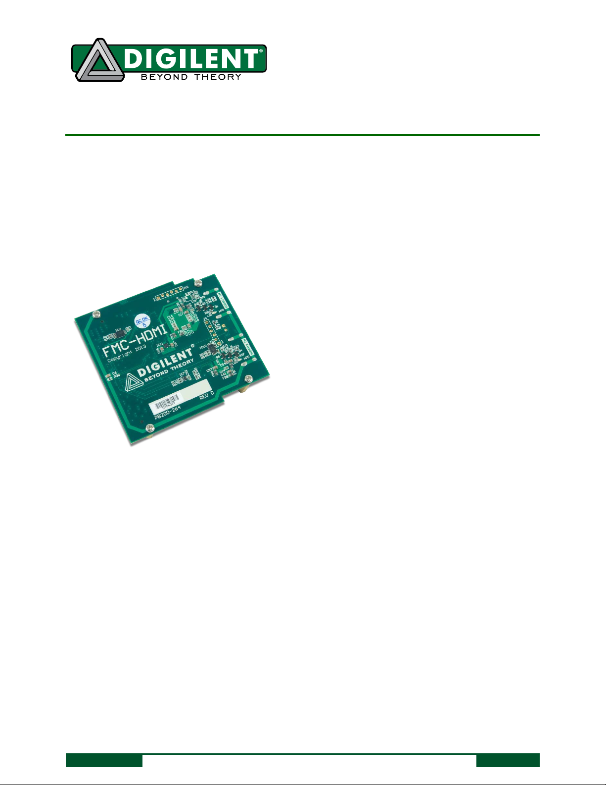
Figure 1. FMC-HDMI.
2 Functional Description
The FMC-HDMI card contains two HDMI input ports. The first port, HDMI1, contains an ADI ADV7611 Receiver and
outputs a decoded, level translated digital video signal to the FMC connector. The second port, HDMI2, contains an
ADI AD8195 Buffer and outputs an HDMI-encoded signal to the FMC connector, leaving the system board to
decode the signal (either in the FPGA or an external receiver).
The appropriateness of the HDMI port depends entirely on the application. For instance, although HDMI2 does not
decode the signal, it outputs to a smaller number of pins (14 instead of 36), which is useful in designs with limited
input availability. Since the decoding must be done on the connected system board, the circuitry must support
HDMI-type signaling that is TMDS. For example, Xilinx® FPGA families support the TMDS_33 input standard in 3.3Vpowered I/O banks.
2.1 HDMI1: Analog Devices ADV7611 Receiver
An Analog Devices ADV7611 Receiver decodes the signal on HDMI1. This low power, 165 MHz receiver supports
formats up to UXGA 60Hz at 8 bit at 161 MHz. It has been tested at WUXGA (1080p) 60Hz at 148.5 MHz. The
receiver provides an audio output port for audio extracted from the HDMI signal in the following formats: I
2
S,
DOC#: 502-264
Other produc t and company names mentioned may be tra demarks of their respective owners.
Copyright Digilent, Inc. All rights reserve d.
Page 1 of 3
Page 2
FMC-HDMI Reference Manual
S/PDIF, and Direct Stream Transfer (DST). It also features an advanced mute controller.
The ADV7611 Receiver contains several other features, such as a CEC 1.4-compatible controller for consumer
device remote control and discovery and EDID (Extended Display Identification Data) RAM.
Note: For more information on the ADV7611, see ADI datasheets and User Guide available online at:
http://www.analog.com/ADV7611
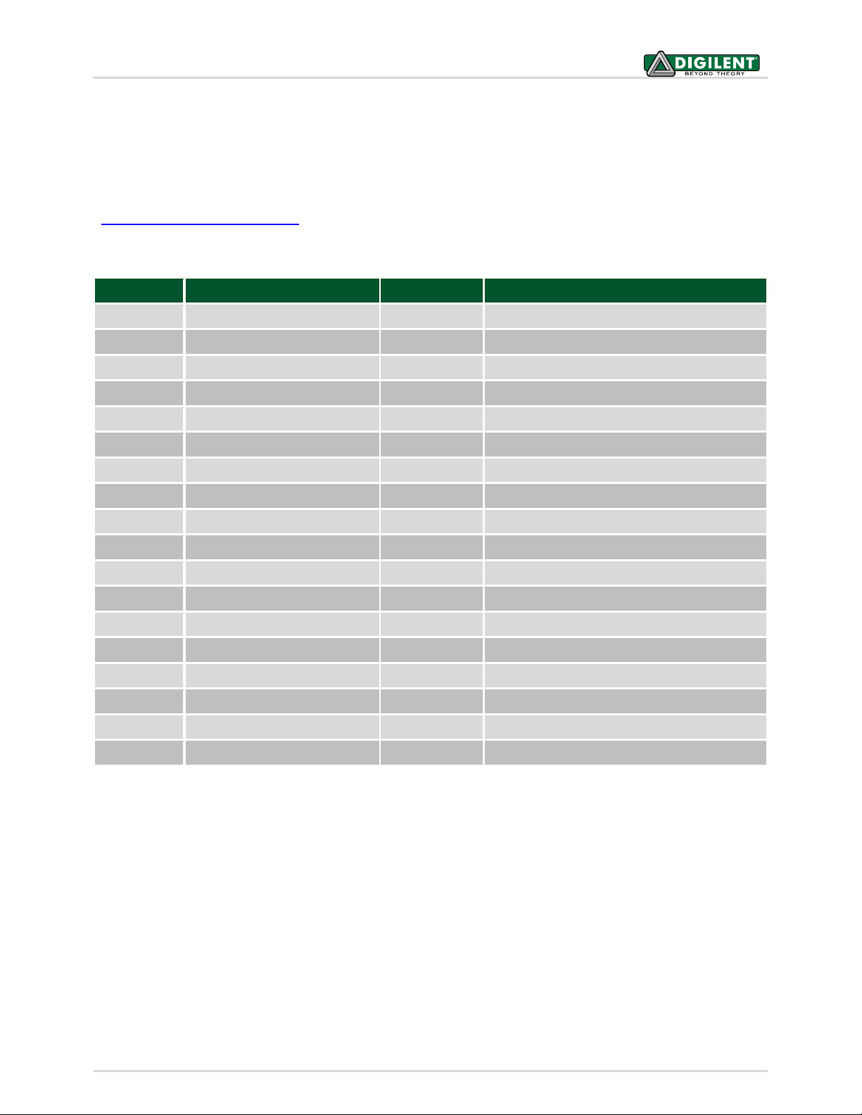
Below are the pin-outs from the ADV7611 Receiver and other HDMI1 port signals to the FMC connector:
FMC Pin HDMI1 Function FMC Pin HDMI1 Function
LA19_P HDMI1_P0 LA04_P HDMI1_P18
LA20_N HDMI1_P1 LA03_N HDMI1_P19
LA20_P HDMI1_P2 LA03_P HDMI1_P20
LA15_N HDMI1_P3 LA02_N HDMI1_P21
LA14_N HDMI1_P4 LA02_P HDMI1_P22
LA15_P HDMI1_P5 LA00_N_CC HDMI1_P23
LA16_N HDMI1_P6 LA18_P_CC HDMI1_SCLK
LA16_P HDMI1_P7 LA21_P HDMI1_LRCLK
LA11_N HDMI1_P8 LA17_P_CC HDMI1_MCLK
LA14_P HDMI1_P9 LA23_N HDMI1_AP
LA11_P HDMI1_P10 LA22_P HDMI1_VS
LA12_N HDMI1_P11 LA19_N HDMI1_HS
LA12_P HDMI1_P12 LA22_N HDMI1_DE
LA07_N HDMI1_P13 LA00_P_CC HDMI1_LLC
LA08_N HDMI1_P14 LA25_P HDMI1_SDA
LA07_P HDMI1_P15 LA21_N HDMI1_SCL
LA08_P HDMI1_P16 LA23_P HDMI1_RESETN
LA04_N HDMI1_P17 LA25_N HDMI1_INT1
Table 1. HDMI1-FMC pin mapping.
The ADV7611 is configured and controlled via an I2C interface, which is accessible through the HDMI1SDA and
HDMI1SCL pins on the FMC connector. The ADV7611 User Guide specifically describes the different registers and
commands necessary to control the Receiver.
There are level translators present on all audio and video signals, which can level shift to 1.8V, 2.5V, and 3.3V. The
desired level is set by the VADJ voltage level.
2.2 HDMI2: Analog Devices AD8195 Buffer
The AD8195 is an HDMI buffer with equalized TMDS inputs and optionally pre-emphasized TMDS outputs. The
AD8195 includes bidirectional buffering for the DDC bus and bidirectional buffering with integrated pull-up
resistors for the CEC bus. The DDC and CEC buffers are powered independently of the TMDS buffers so that
DDC/CEC functionality can be maintained when the system is powered off.
Copyright Digilent, Inc. All rights reserve d.
Other produc t and company names mentioned may be tra demarks of their respective owners.
Page 2 of 3
Page 3
FMC-HDMI Reference Manual
An on-board pre-programmed EEPROM is connected to the DDC (Display Data Channel) bus of the HDMI2 port.
The following EDID (Extended Display Identification Data) is programmed in the factory:
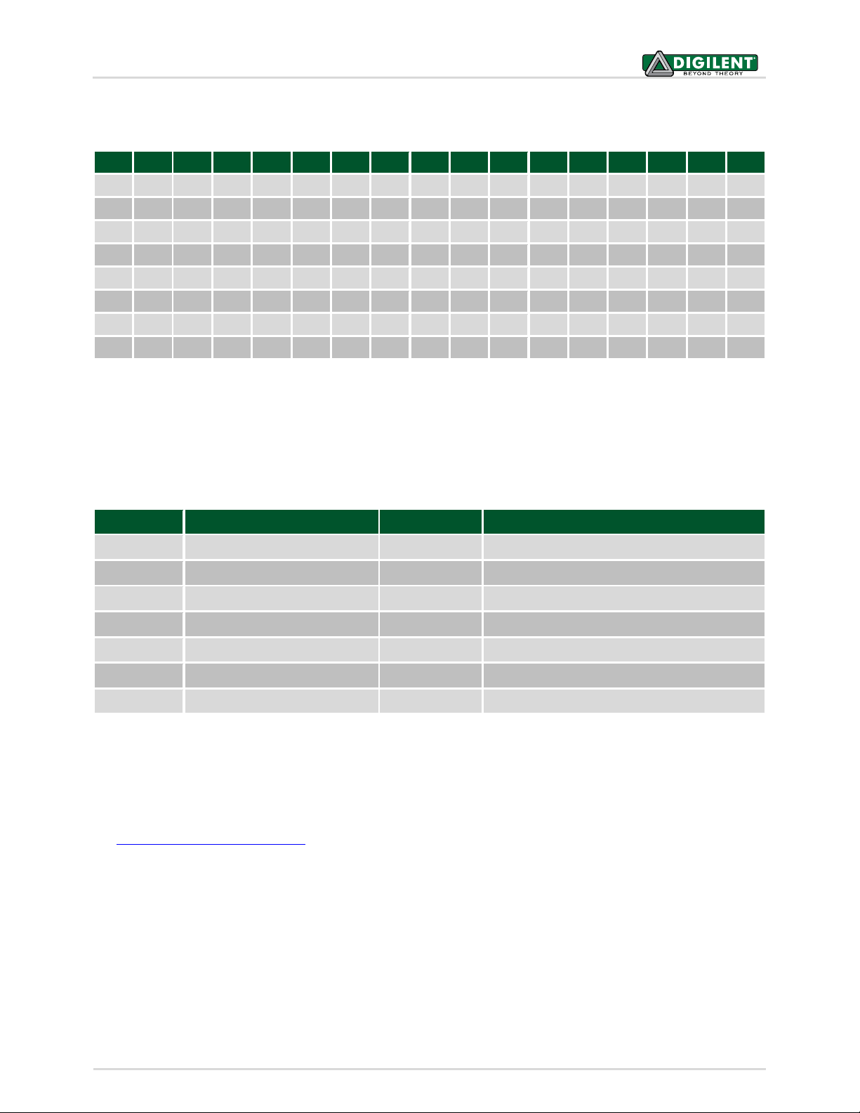
00 01 02 03 04 05 06 07 08 09 0A 0B 0C 0D 0E 0F
00 0x00 0xFF 0xFF 0xFF 0xFF 0xFF 0xFF 0x00 0x10 0xEC 0x00 0x01 0x00 0x00 0x00 0x00
10 0xFF 0x16 0x01 0x03 0x81 0x33 0x1D 0x78 0x02 0x01 0xF1 0xA2 0x57 0x52 0x9F 0x27
20 0x0A 0x50 0x54 0xBF 0xEF 0x80 0x01 0x01 0x01 0x01 0x01 0x01 0x01 0x01 0x01 0x01
30 0x01 0x01 0x01 0x01 0x01 0x01 0x01 0x1D 0x00 0x72 0x51 0xD0 0x1E 0x20 0x6E 0x28
40 0x55 0x00 0x00 0xD0 0x52 0x00 0x00 0x1E 0x00 0x00 0x00 0xFC 0x00 0x44 0x69 0x67
50 0x69 0x6C 0x65 0x6E 0x74 0x20 0x48 0x44 0x4D 0x49 0x00 0x00 0x00 0x10 0x00 0x00
60 0x00 0x00 0x00 0x00 0x00 0x00 0x00 0x00 0x00 0x00 0x00 0x00 0x00 0x00 0x00 0x10
70 0x00 0x00 0x00 0x00 0x00 0x00 0x00 0x00 0x00 0x00 0x00 0x00 0x00 0x00 0x00 0x0E
Table 2. EEPROM pre-programmed content.
The EEPROM can be freely re-written through the J4 header holes and 6-pin Pmod cable. During EEPROM
programming, power to the EEPROM is provided by pin 6 of J4, so make sure there is no HDMI cable plugged in at
the same time.
Below are the pin-outs from the AD8195 Buffer and other HDMI2 port signals to the FMC connector:
FMC Pin HDMI2 Function FMC Pin HDMI2 Function
LA06_P HDMI2_D0_P LA01_N_CC HDMI2_CLK_N
LA06_N HDMI2_D0_N LA13_P HDMI2_SCL
LA05_P HDMI2_D1_P LA13_N HDMI2_SDA
LA05_N HDMI2_D1_N LA09_P HDMI2_PE_EN
LA10_P HDMI2_D2_P LA09_N HDMI2_TX_EN
LA10_N HDMI2_D2_N LA17_N_CC HDMI2_HPA
LA01_P_CC HDMI2_CLK_P LA18_N_CC HDMI2_CEC_OUT
Table 3. HDMI2-FMC pin mapping.
WARNING: VADJ must be 3.3V to properly use the buffer on HDMI2. The TX_EN pin is held low by default, so the
buffer is disabled on power-up. With the buffer disabled, VADJ can be in the range of (1.8V-3.3V).
Note: For more information on the AD8195, see ADI datasheets available online
at http://www.analog.com/AD8195
2.3 FMC Support
The FMC-HDMI uses a Samtec ASP-134604-01 low pin-count male connector as the main connector for digital
signals. The board fully conforms to the VITA 57.1 specs. The connector supports the full range of 1.8V-3.3V bank
supply voltages (VADJ).
The EEPROM with designator IC2 (see board schematic) serves as the IPMI EEPROM, providing hardware definition
information. For more information, consult the VITA 57.1 specs.
Copyright Digilent, Inc. All rights reserve d.
Other produc t and company names mentioned may be tra demarks of their respective owners.
Page 3 of 3
 Loading...