

Page 1
1300 Henley Court
Pullman, WA 99163
509.334.6306
www.digilentinc.com
JTAG-SMT1™ Programming Module for Xilinx® FPGAs
Revised March 2, 2015
This manual applies to the JTAG-SMT1 rev. A
DOC#: 502-203
Copyright Digilent, Inc. All rights reserved.
Other product and company names mentioned may be trademarks of their respective owners.
Page 1 of 5
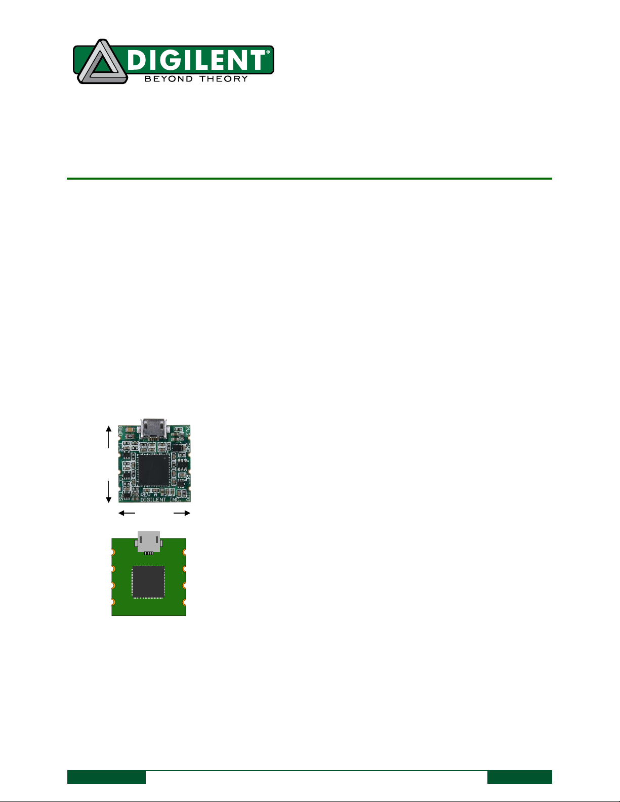
21.5mm
23 mm
1
2
3
4
8
7
6
5
GND
TCK
TDI
TMS
Vdd (3.3V)
GND
VREF
TDO
The JTAG-SMT1.
Small, complete, all-in-one JTAG programming solution for
Xilinx FPGAs
Single 3.3V supply
Separate Vref drives JTAG signal voltages; Vref can be any
voltage between 1.8V and 5V.
High-Speed USB2 port that can drive JTAG/SPI bus at up to
30Mbit/sec
Able to drive JTAG bus at up to 30Mbit/sec
JTAG/TCK frequency settable by user
Compatible with all Xilinx tools
Small form-factor surface-mount module can be directly
loaded on target boards
Uses micro-AB USB2 connector
Same circuit is available as a stand-alone programming cable;
see Digilent’s JTAG-HS1.
Features include:
Overview
The JTAG-SMT1 is a compact, complete, and fully self-contained surface-mount programming module for Xilinx®
FPGAs. It can be accessed directly from all Xilinx Tools, including iMPACT, ChipScope™, and EDK. The module can
be loaded directly onto a target board and reflowed like any other component.
The JTAG-SMT1 uses a 3.3V main power supply and a separate Vref supply to drive the JTAG signals. All JTAG
signals use high speed, 24mA, three-state buffers that allow signal voltages from 1.8V to 5V and bus speeds of up
to 30MBit/sec. JTAG signals are actively driven only during a programming event and are otherwise held in highimpedance, so the JTAG bus can be shared with other devices.
The SMT1 module is CE certified and fully compliant with the RoHS and REACH directives. It uses a standard Type-A
to Micro-USB cable, also available from Digilent.
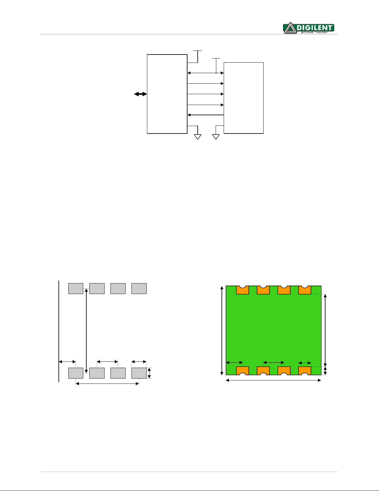
The JTAG signals can be connected directly to the corresponding FPGA signals, as shown in the image below. For
best results, the module should be mounted adjacent to the edge of the host PCB over a ground plane. Although
signal traces may be run on top of the host PCB beneath the SMT1, it is recommended the area immediately
beneath the SMT1 be kept clear. For highest speed JTAG operation, impedance between the SMT1 and FPGA
should be kept below 100 Ohms.
Page 2
JTAG-SMT1 Programming Module for Xilinx® FPGAs
Copyright Digilent, Inc. All rights reserved.
Other product and company names mentioned may be trademarks of their respective owners.
Page 2 of 5
TCK
JTAG SMT1 FPGA
TMS
TDI
TDO
GND
Vref
VIO
TMS
TCK
TDI
TDO
3.3V
V
IO
GND
Vdd
USB2
Port
2
4
3
5
1
6
8
SMT1 JTAG Port Connections
2 3 41
6 578
3.5mm
2.5mm
5mm4mm
20mm
PCB Edge
Recommended PCB pad geometry
15mm
23mm
21.5mm
3mm
5mm
2mm
4mm
17.5mm
SMT1 bottom-up view
Software Support
In addition to working seamlessly with all Xilinx tools, the SMT1 is supported by Digilent's Adept software and the
Adept SDK (the SDK can be freely downloaded from Digilent’s website). Adept includes a full-featured
programming environment, and a set of public APIs that allow user applications to directly drive the JTAG chain.
Using the SDK, custom applications can be created to drive JTAG ports on virtually any device. The SDK also
supports SPI ports, allowing applications to drive any SPI device using SPI Mode 0 or Mode 2. Please see the Adept
SDK reference manual for more information.
Mechanical Information
Page 3

JTAG-SMT1 Programming Module for Xilinx® FPGAs
Copyright Digilent, Inc. All rights reserved.
Other product and company names mentioned may be trademarks of their respective owners.
Page 3 of 5
Symbol
Parameter
Condition
Min
Max
Unit
Vdd
Operating supply voltage
-0.3
4.0
V
Vref
I/O reference/supply voltage
-0.3
6
V
VIO
Signal Voltage
-0.3
6
V
IIK,IOK
TMS, TCK, TDI, TDO
DC Input/Output Diode Current
VIO < -0.3V
-50
mA
VIO > 6V
+20
I
OUT
DC Output Current
±50
mA
T
STG
Storage Temperature
-20
+120
ºC
ESD
Human Body Model JESD22-A114
2000
V
Charge Device Model JESD22-C101
500
V
Symbol
Parameter
Min
Typ
Max
Unit
Vdd
Operating supply voltage
2.97
3.3
3.63
Volts
Vref
I/O reference/supply voltage
1.65
2.5/3.3
5.5
Volts
TDO
Input High Voltage (VIH)
0.75 x Vref
5.5
Volts
Input Low Voltage (VIL)
0
0.25 x Vref
Volts
TMS, TCK, TDI
Output High (VOH)
0.85 x Vdd
0.95 x Vdd
Vdd
Volts
Output Low (VOL)
0
0.05 x Vdd
0.15 x Vdd
Volts
Absolute Maximum Ratings
DC Operating Characteristics
AC Operating Characteristics
SMT1 JTAG signals are driven according to the timing diagram below. JTAG/TCK frequencies from 30 MHz to 8 KHz
are supported, at integer divisions of 30 MHz from 1 to 3750. Common frequencies include 30 MHz, 15 MHz, 10
MHz, 7.5 MHz, and 6 HMz. JTAG/TCK operating frequency can be set from within the Xilinx tools.
Note: Please refer to Xilinx’s iMPACT documentation for more information.
Page 4

JTAG-SMT1 Programming Module for Xilinx® FPGAs
Copyright Digilent, Inc. All rights reserved.
Other product and company names mentioned may be trademarks of their respective owners.
Page 4 of 5
0
50
100
150
200
250
300
-15 5 25
45
65
85
105
125
145
165
185
205
225
245
265
285
305
325
345
365
385
Reflow Temp. (
o
C)
Reflow Time (s)
JTAG SMT1 Profile
Symbol
Parameter
Min
Max
TCK
TCK period
33ns
2.185ms
T
CKH
, T
CKL
T
CLK
pulse width
20ns
1.1ms
TCD
T
CLK
to TMS, TDI
0
15ns
TSU
TDO Setup time
19ns
THD
TDO Hold time
0
TMS/TDI
TCK
TDO
T
CKL
T
CKH
T
CK
T
CD
T
SU
T
HD
Mounting to Host PCBs
The JTAG-SMT1 module has a moisture sensitivity level (MSL) of 6. Prior to reflow, the JTAG-SMT1 module must be
dried by baking it at 125° C for 17 hours. Once this process has been completed, the module has a MSL of 3 and is
suitable for reflow for up to 168 hours without additional drying.
SMT1 signal pads are finished with the ENIG process using 2u” gold over 150u” electroless nickel. The SMT1 is
compatible with most mounting and reflow processes. The binding force of the solder is sufficient to hold the
SMT1 firmly in place; no additional adhesives are required.
Page 5

JTAG-SMT1 Programming Module for Xilinx® FPGAs
Copyright Digilent, Inc. All rights reserved.
Other product and company names mentioned may be trademarks of their respective owners.
Page 5 of 5
35cm
28cm
Packaging
Small quantities (less than 20 per order) will be individually packaged in antistatic bags for shipping. Larger
quantities will be packed in 80 position antistatic bubble trays.
 Loading...