

Page 1
VVmmooddCCAAMM™™ RReeffeerreennccee MMaannuuaal
Revision: July 19, 2011
Note: This document applies to REV C of the board.
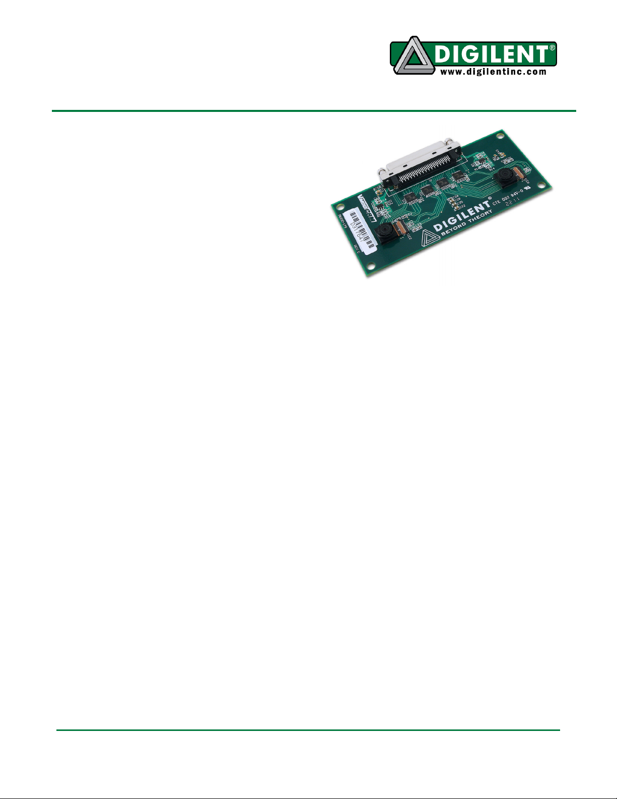
Overview
The VmodCAM board provides digital imaging
capabilities for any Digilent FPGA system
board with a VHDCI connector. It features two
Aptina MT9D112 2-megapixel CMOS digital
image sensors. The sensors can provide frame
rates from 15 FPS upwards, depending on the
resolution.
Its system-on-a-chip design integrates an
image flow processor and enables selectable
output formats, scaling, and special effects.
The integrated PLL (phase-locked loop) and
microprocessor offer a flexible serial control
interface. The output data is sent on a parallel
bus in processed YCrCb, RGB, or raw Bayer
formats.
Features include:
• two independent Aptina MT9D112 2megapixel CMOS digital image sensors
• 1600x1200 maximum resolution at 15
FPS
• 63mm inter-camera spacing (stereo
baseline)
• 10-bit raw color depth
• I2C control bus
• Bayer, RGB, YCrCb output formats
• automatic exposure, gain, and white
balance
• powerful image correction algorithms
• image scaling
• output FIFO
• 68-pin female VHDCI connector
Functional Description
The two MT9D112 cameras can be controlled
independently and can acquire two separate,
simultaneous image feeds. They are controlled
by a two-wire interface.
l
1300 NE Henley Court, Suite 3
Pullman, WA 99163
(509) 334 6306 Voice | (509) 334 6300 Fax
Each camera has a 2 megapixel color sensor
array in Bayer color filter arrangement. The
sensor readout is 10-bit and supports skipping
or binning rows/columns.
The integrated PLL can generate an internal
clock from the master clock and supports a
wide range of resolutions and frame rates.
The integrated image flow processor applies
correction algorithms to improve image quality.
It can process raw sensor data into RGB or
YCrCb output formats, and crop or scale the
image.
Since some of the processing algorithms
output data in bursts, the parallel output
interface can use a FIFO buffer to provide
constant data rate.
The camera also features a sequencer to
coordinate events triggered by the user.
Operation
The camera systems first need to be properly
configured. This includes not only setting
imaging parameters like resolution or output
format, but PLL configuration and
microprocessor sequencing too. The order in
which these steps are performed is very
important.
Doc: 502-179 page 1 of 6
Copyright Digilent, Inc. All rights reserved. Other product and company names mentioned may be trademarks of their respective owners.
Page 2
VmodCAM Reference Manual
First, you must set up the power-up and reset
sequence. Then you need to understand the
control interface in order to configure the
cameras. The following sections describe this
in detail.
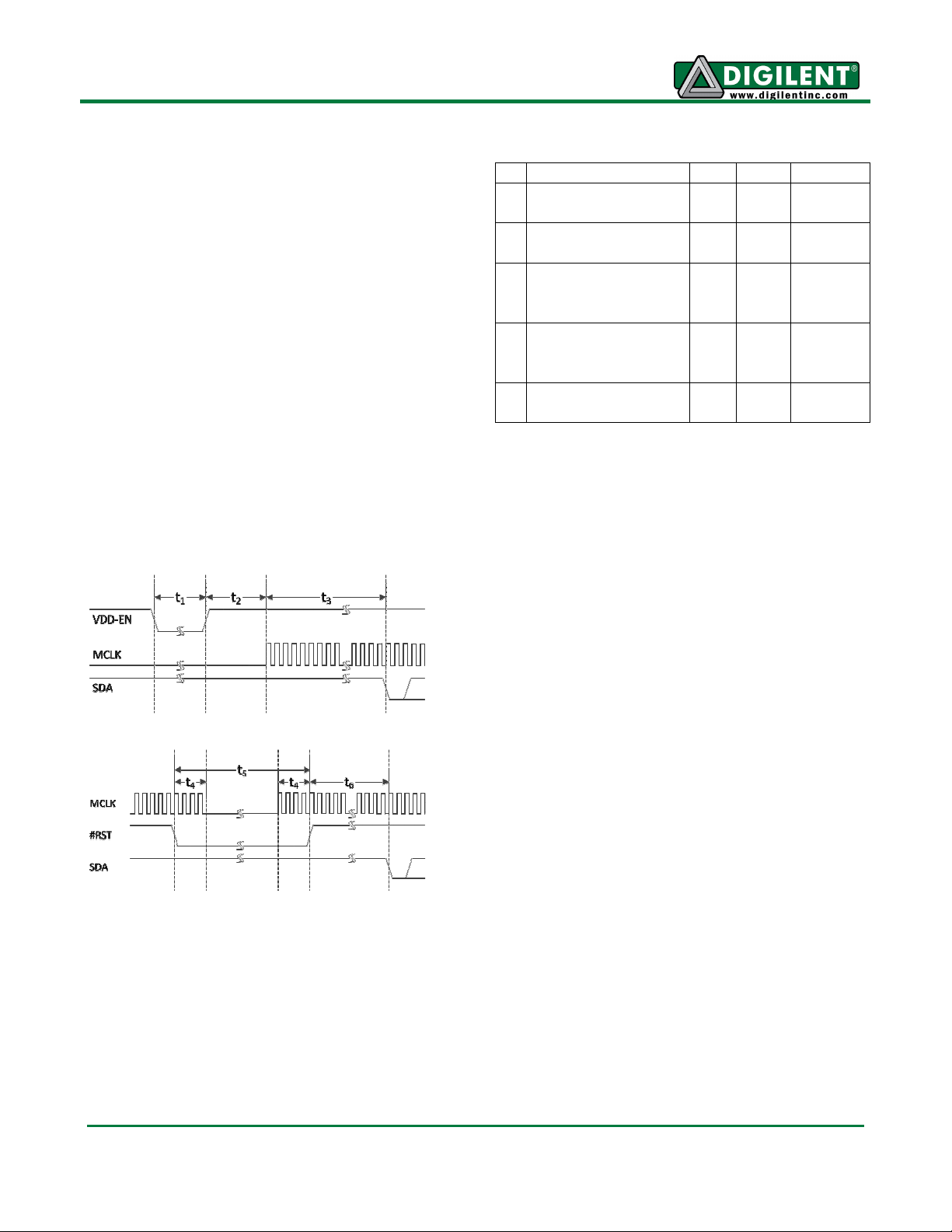
Power-Up and Reset Sequence
The VmodCAM should only be attached to the
system board once the signals driven by the
system board are defined.
The camera uses the analog and digital supply
voltage rails provided on-board. The power
supplies are on by default, but can be turned
off, by driving the VDD-EN signal low (see
Table 3.)
The power supplies are used by both cameras.
While the cameras do power-on reset
themselves, it’s always a good idea to do a full
reset as part of the controller routine.
Figure 1 Power-Up Sequence
Figure 2 Reset Sequence
The MCLK is important. If the PLL in the
camera is enabled, MCLK should be stable.
Stopping MCLK without respecting the reset
sequence might leave the camera in an
undefined state. This could be the case when
the FPGA is re-configured. Performing a
power-cycle in the first stages of the controller
is recommended.
Description Min Max Unit
t1 VDD-EN negative
100
ms
pulse width
t2 VDD-EN high to
75 us
first MCLK pulse
t3
ROM read time
t6
until first control
6000 MCLK
cycles
byte
t4 Active MCLK
before/after #RST
10 MCLK
cycles
edge
t5 #RST negative
pulse width
Table 1 Power-Up/Reset Timing
30 MCLK
cycles
Control Interface
The two-wire serial interface (SDA, SCL) can
be used to control various parts of the camera.
The camera acts as a slave device.
A typical register write consists of:
• start condition
• 8-bit device address (0x78 for the
MT9D112) + acknowledge bit
• upper byte of 16-bit register address +
acknowledge bit
• lower byte of register address +
acknowledge bit
• upper byte of the 16-bit data +
acknowledge bit
• lower data byte + acknowledge bit
• stop condition.
www.digilentinc.com page 2 of 6
Copyright Digilent, Inc. All rights reserved. Other product and company names mentioned may be trademarks of their respective owners.
Page 3

VmodCAM Reference Manual
A register read consists of:
• start condition
• 8-bit device address (0x78 for the
MT9D112) + acknowledge bit
• upper byte of 16-bit register address +
acknowledge bit
• lower byte of register address +
acknowledge bit
• start condition
• 8-bit device address (0x79 for the
MT9D112) + acknowledge bit
• upper byte of the 16-bit data +
acknowledge bit
• lower data byte + no-acknowledge bit
• stop condition.
There are two types of configuration controls,
hardware registers and driver variables. The
hardware registers usually control the sensor
and some other sub-systems, while the driver
variables sequence the on-chip
microprocessor. These two types of controls
are accessed differently.
Hardware registers are two-wire accessible,
meaning their address can be used directly in
the register address phase of the two-wire
transfer. Hardware registers are referred to by
their address. For example, R[0x3000] refers
to the register located at address 0x3000.
Driver variables can be accessed via two
hardware registers, R[0x338C] and R[0x3390].
To access a variable, its address first needs to
be written to R[0x338C], which is a standard
two-wire register write. Then, reading register
R[0x3390] reads the variable and writes a
value to it, thus setting the variable to that
value. Driver variables are referred to by their
address. For example, V[0x2797] refers to the
driver variable located at address 0x2797.
Configuration
The cameras start up with their registers set to
default values. This also means they are in
standby. To acquire images from the cameras,
both have to be initialized properly. As the
power-on and reset sequences show, the
camera needs certain signals set and a
running MCLK before the two-wire interface is
enabled.
Once the necessary number of MCLK cycles
are provided, the following registers/variables
need to be read/written.
Identify the camera:
To verify that the camera is working, read
R[0x3000] to return 0x1580, which is the
device ID of the camera.
Reset the MCU:
1. R[0x3386] = 0x0501
2. R[0x3386] = 0x0500; release from reset
Set the PLL:
1. R[0x3214] = 0x0D85; this sets the slew
rate of the output pins
2. R[0x341E] = 0x8F0B; power-down and
bypass PLL; if you want to use MCLK
as the pixel clock, skip steps 3-5.
3. R[0x341C][13:8] = N
R[0x341C][7:0] = M;
Where PCLK = MCLK * M / (N+1) / 8.
For example, to obtain a pixel clock of
80MHz (maximum) from an MCLK of
24MHz, set M=80, N=2.
4. R[0x341E] = 0x8F09; power up PLL,
wait 1ms for the PLL to stabilize
5. R[0x341E] = 0x8F08; use PLL clock
instead of MCLK
Wake up from standby:
1. R[0x3202] = 0x0008
Insert image parameters:
You can change the image parameters to suit
your project. See the Image Configuration
Example below to insert an image parameter
configuration sequence.
www.digilentinc.com page 3 of 6
Copyright Digilent, Inc. All rights reserved. Other product and company names mentioned may be trademarks of their respective owners.
Page 4

VmodCAM Reference Manual
Enable output:
1. R[0x301A] = 0x02CC; parallel enable,
drive pins, start streaming.
Image Processing
Raw sensor data coming from the pixel array is
fed to a color processing pipeline called an
image flow processor (IFP). This is where all
the image processing, correction, scaling,
interpolation, and output formatting algorithms
are applied.
The IFP can also be bypassed, causing the
camera to output the uncompressed raw 10-bit
Bayer data in this mode.
The IFP is controlled indirectly, through
microprocessor variables and the sequencer.
The IFP can be controlled directly by
accessing its hardware registers, but normally
the on-chip microprocessor regularly adjusts
these parameters.
Output Formats
Mode Byte D7:D0
RGB565 Odd R7R6R5R4R3G7G6G
Even G4G3G2B7B6B5B4B3
RGB555 Odd 0R7R6R5R4R3G7G6
Even G5G4G3B7B6B5B4B3
RGB444x Odd R7R6R5R4G7G6G5G
Even B7B6B5B40000
RGBx444 Odd 0000R7R6R5R4
Even G7G6G5G4B7B6B5B4
YUV 4*i Cb
4*i+1 Y
4*i+2 Cr
4*i+3 Y
Contexts
The microprocessor uses two contexts, each
with their own set of parameters. Context A is
preconfigured for preview mode. Context B is
for snapshot and video capture.
You can set the parameters using the two-wire
interface to command the sequencer to switch
contexts. If the parameters being modified
belong to the active mode, the changes only
take effect after the Refresh and Refresh Mode
commands are executed.
Sequencer
The sequencer is a state machine responsible
for coordinating events triggered by the user.
You can query the current state and instruct
the sequencer to change state.
The sequencer command variable V[0xA103]
accepts the following values:
• 0-Run
• 1-Go to Preview
• 2-Go to Capture
• 3-Go to Standby
• 4-Do lock
• 5-Refresh
• 6-Refresh mode
For the video capture, the Video bit (bit 1)
5
needs to set in variable V[0xA120]. Otherwise,
the capture state will only take a single
snapshot.
4
The sequencer state variable V[0xA104] reads:
• 0-Initialize
• 1-Mode Change to Preview
• 2-Enter Preview
• 3-Preview
• 4-Leave Preview
• 5-Mode Change to Capture
• 6-Enter Capture
• 7-Capture
• 8-Leave Capture
• 9-Standby
www.digilentinc.com page 4 of 6
Copyright Digilent, Inc. All rights reserved. Other product and company names mentioned may be trademarks of their respective owners.
Page 5

VmodCAM Reference Manual
0 4
0 4
11
10
0 0
0 0
8
4
3
2
0
Variable Address
Description Context A
Context B Bits
Current Context (0 = A, 1 = B) 0xA702 7:0
Output Width 0x2703
Output Height 0x2705
Sensor Row Start 0x270D
Sensor Row End 0x2711
Sensor Column Start 0x270F
Sensor Column End 0x2713
Read Mode 0x2719
0x2707 15:0
0x2709 15:0
0x272F 15:0
0x2733 15:0
0x2731 15:0
0x2735 15:0
0x273B 15:0
x-bin enable
xy-bin enable
x odd increment 7:5
y odd increment 4:2
vertical flip
(0=normal)
horizontal flip
(0=normal)
Crop X0 0x2751
Crop X1 0x2753
Crop Y0 0x2755
Crop Y1 0x2757
Output format 0x2795
0x275F 15:0
0x2761 15:0
0x2763 15:0
0x2765 15:0
0x2797 15:0
processed Bayer mode
RGB output format
0x0=RGB565
0x1=RGB555
7:6
0x2=RGB444x
0x3=RGBx444
RGB/YUV
0x1=RGB
0x0 = YUV
Use CCIR656 codes when bypassing FIFO
Monochrome output
Progressive Bayer
Swap chrominance/luminance bytes in YUV, swap odd/even bytes in
RGB
Swap Cr/Cb in YUV, swap R/B in RGB
Default
Context A Context
800
600
1213
1613
0x046C
0x0
0x1
0x3
0x3
1
0
0x0
0x0
800
600
0x0000
0x0
0x0
5
0x0
0x0
0x0
0x0
1
0x0
0x0
B
0x0000
1600
1200
1211
1611
0x0024
0x0
0x0
0x1
0x1
0x0
0x0
1600
1200
0x0000
0x0
0x0
0x0
0x0
0x0
0x0
0x0
0x0
Table 2 Image Parameters
www.digilentinc.com page 5 of 6
Copyright Digilent, Inc. All rights reserved. Other product and company names mentioned may be trademarks of their respective owners.
Page 6

VmodCAM Reference Manual
Image Configuration Example
The following commands can be inserted into
the initialization sequence to configure the
camera for 16-bit RGB565 output and
1600x1200 resolution in video capture mode.
Note that most of these parameters are driver
variables and can be accessed as described in
the
Control Interface section above.
1. V[0x2797] = 0x0030; Context B output
format RGB565
2. V[0x2707] = 0x0640; Output width 1600
3. V[0x2709] = 0x04B0; Output height
1200
4. V[0x275F] = 0x0000; Crop X0 0
5. V[0x2763] = 0x0000; Crop Y0 0
6. V[0x2761] = 0x0640; Crop X1 1600
7. V[0x2765] = 0x04B0; Crop X1 1200
8. V[0x2741] = 0x0169; Auto
exposure/gain fix
9. V[0xA120] = 0x00F2; Auto White
Balance, Auto Exposure, Auto
Histogram, Video On in Capture mode
10. V[0xA103] = 0x0002; Sequencer
Refresh Mode
11. Read V[0xA103] until == 0x0000,
meaning the command got executed.
CAM1 refers to IC2, the camera on the lower
part of the PCB.
CAM2 refers to IC6, the camera on the upper
part of the PCB.
Camera Output Camera Input
VHDCI CAM VHDCI CAM
IO1-P CAM1_D3 IO1-N VDD-EN
IO2-P CAM1_D4 IO2-N CAM1_D2
IO3-P CAM1_D5 IO3-N CAM1_RESET
IO4-P CAM1_D6 IO4-N CAM1_MCLK
IO5-P CAM1_D7 IO5-N CAM1_PWDN
IO6-P CAM1_FV IO6-N CAM1_SCL
IO7-P CAM1_LV IO7-N CAM1_SDA
IO8-P CAM1_D0 IO8-N NC
IO9-P CAM1_D1 IO9-N NC
IO10-P CAM1_PCLK IO10-N NC
IO11-P CAM2_PCLK IO11-N NC
IO12-P CAM2_D2 IO12-N CAM2_PWDN
IO13-P CAM2_D3 IO13-N CAM2_RESET
VHDCI Connector
The VmodCAM should only be attached to the
system board once the signals driven by the
IO14-P CAM2_D4 IO14-N CAM2_MCLK
IO15-P CAM2_D5 IO15-N NC
IO16-P CAM2_D6 IO16-N CAM2_SCL
system board are defined.
IO17-P CAM2_D7 IO17-N CAM2_SDA
IO18-P CAM2_FV IO18-N NC
IO19-P CAM2_LV IO19-N NC
IO20-P CAM2_D0 IO20-N CAM2_D1
Table 3 VHDCI Connector Pin-Out
www.digilentinc.com page 6 of 6
Copyright Digilent, Inc. All rights reserved. Other product and company names mentioned may be trademarks of their respective owners.
 Loading...