

Page 1

72000 Bluetooth Development Kit
User’s Guide
94001620000
Rev. 1.2 TR special, 2002-12-06
Page 2

Motorola reserves the right to make changes without further notice to any products herein. Motorola makes no warranty,
representation or guarantee regarding the suitability of its products for any particular purpose, nor does Motorola assume any liability
arising out of the application or use of any product or circuit, and specifically disclaims any and all liability, including without limitation
consequential or incidental damages. “Typical” parameters which may be provided in Motorola data sheets and/or specifications can
and do vary in different applications and actual performance may vary over time. All operating parameters, including “Typicals” must
be validated for each customer application by customer’s technical experts. Motorola does not convey any license under its patent
rights nor the rights of others. Motorola products are not designed, intended, or authorized for use as components in systems
intended for surgical implant into the body, or other applications intended to support life, or for any other application in which the
failure of the Motorola product could create a situation where personal injury or death may occur. Should Buyer purchase or use
Motorola products for any such unintended or unauthorized application, Buyer shall indemnify and hold Motorola and its officers,
employees, subsidiaries, affiliates, and distributors harmless against all claims, costs, damages, and expenses, and reasonable
attorney fees arising out of, directly or indirectly, any claim of personal injury or death associated with such unintended or
unauthorized use, even if such claim alleges that Motorola was negligent regarding the design or manufacture of the part. The
Bluetooth trademarks are owned by their proprietor and used by Motorola, Inc., under license. All other product or service names are
the property of their respective owners. © Motorola, Inc. 2002.
Motorola and are registered trademarks of Motorola, Inc. Motorola, Inc. is an Equal Opportunity/Affirmative Action Employer.
How to reach us:
USA/EUROPE/Locations Not Listed: Motorola Literature Distribution; P.O. Box 5405, Denver, Colorado, 80217.
1–303–675–2140 or 1–800–441–2447
JAPAN: Motorola Japan Ltd.; SPS, Technical Information Center, 3–20–1, Minami–Azabu, Minato–ku,
Tokyo 106–8573 Japan. 81–3–3440–3569
ASIA/PACIFIC: Motorola Semiconductors H.K. Ltd., Silicon Harbour Centre, 2 Dai King Street,
Tai Po Industrial Estate, Tai Po, N.T., Hong Kong. 852–26668334
Technical Information Center: 1–800–521–6274
HOME PAGE: http://www.motorola.com/semiconductors/
© Copyright Motorola, Inc., 2002
Page 3

Contents
Chapter 1
Introduction
1.1 About This Guide . . . . . . . . . . . . . . . . . . . . . . . . . . . . . . . . . . . . . . . . . . . . . . . . . . . . . . 1-1
1.2 Additional Documents . . . . . . . . . . . . . . . . . . . . . . . . . . . . . . . . . . . . . . . . . . . . . . . . . . 1-2
1.3 Downloads and Support . . . . . . . . . . . . . . . . . . . . . . . . . . . . . . . . . . . . . . . . . . . . . . . . . 1-3
1.4 System Requirements . . . . . . . . . . . . . . . . . . . . . . . . . . . . . . . . . . . . . . . . . . . . . . . . . . . 1-3
1.5 Acronyms and Abbreviations . . . . . . . . . . . . . . . . . . . . . . . . . . . . . . . . . . . . . . . . . . . . . 1-4
Chapter 2
Product Overview
2.1 Block Diagram . . . . . . . . . . . . . . . . . . . . . . . . . . . . . . . . . . . . . . . . . . . . . . . . . . . . . . . . 2-5
2.2 Interfaces. . . . . . . . . . . . . . . . . . . . . . . . . . . . . . . . . . . . . . . . . . . . . . . . . . . . . . . . . . . . . 2-6
2.3 ICs. . . . . . . . . . . . . . . . . . . . . . . . . . . . . . . . . . . . . . . . . . . . . . . . . . . . . . . . . . . . . . . . . . 2-6
2.4 Software Tools . . . . . . . . . . . . . . . . . . . . . . . . . . . . . . . . . . . . . . . . . . . . . . . . . . . . . . . . 2-6
2.4.1 Bluetooth HCI Terminal. . . . . . . . . . . . . . . . . . . . . . . . . . . . . . . . . . . . . . . . . . . . . . 2-6
2.4.2 Configuration Manager. . . . . . . . . . . . . . . . . . . . . . . . . . . . . . . . . . . . . . . . . . . . . . . 2-6
2.4.3 DemoBench . . . . . . . . . . . . . . . . . . . . . . . . . . . . . . . . . . . . . . . . . . . . . . . . . . . . . . . 2-7
2.4.4 RadioTest . . . . . . . . . . . . . . . . . . . . . . . . . . . . . . . . . . . . . . . . . . . . . . . . . . . . . . . . . 2-7
Chapter 3
Setup
Chapter 4
Hardware
4.1 Signal and Connection Descriptions. . . . . . . . . . . . . . . . . . . . . . . . . . . . . . . . . . . . . . . 4-11
4.2 Environmental. . . . . . . . . . . . . . . . . . . . . . . . . . . . . . . . . . . . . . . . . . . . . . . . . . . . . . . . 4-12
4.3 Mechanical . . . . . . . . . . . . . . . . . . . . . . . . . . . . . . . . . . . . . . . . . . . . . . . . . . . . . . . . . . 4-12
4.4 Electrical. . . . . . . . . . . . . . . . . . . . . . . . . . . . . . . . . . . . . . . . . . . . . . . . . . . . . . . . . . . . 4-12
4.4.1 Power Supply . . . . . . . . . . . . . . . . . . . . . . . . . . . . . . . . . . . . . . . . . . . . . . . . . . . . . 4-13
4.4.2 Reset Circuit . . . . . . . . . . . . . . . . . . . . . . . . . . . . . . . . . . . . . . . . . . . . . . . . . . . . . . 4-13
4.4.3 Clocks . . . . . . . . . . . . . . . . . . . . . . . . . . . . . . . . . . . . . . . . . . . . . . . . . . . . . . . . . . . 4-13
4.4.4 Memory. . . . . . . . . . . . . . . . . . . . . . . . . . . . . . . . . . . . . . . . . . . . . . . . . . . . . . . . . . 4-14
4.4.5 UART Interface . . . . . . . . . . . . . . . . . . . . . . . . . . . . . . . . . . . . . . . . . . . . . . . . . . . 4-14
4.4.6 CODEC Interface . . . . . . . . . . . . . . . . . . . . . . . . . . . . . . . . . . . . . . . . . . . . . . . . . . 4-14
4.4.7 Antenna. . . . . . . . . . . . . . . . . . . . . . . . . . . . . . . . . . . . . . . . . . . . . . . . . . . . . . . . . . 4-15
4.4.8 100 mm² Module. . . . . . . . . . . . . . . . . . . . . . . . . . . . . . . . . . . . . . . . . . . . . . . . . . . 4-15
Chapter 5
Regulatory
MOTOROLA Contents iii
Preliminary
Page 4

5.1 Regulatory Statements . . . . . . . . . . . . . . . . . . . . . . . . . . . . . . . . . . . . . . . . . . . . . . . . . 5-17
5.1.1 General . . . . . . . . . . . . . . . . . . . . . . . . . . . . . . . . . . . . . . . . . . . . . . . . . . . . . . . . . . 5-17
5.1.2 European Union (EU) and EFTA . . . . . . . . . . . . . . . . . . . . . . . . . . . . . . . . . . . . . . 5-17
5.1.3 France . . . . . . . . . . . . . . . . . . . . . . . . . . . . . . . . . . . . . . . . . . . . . . . . . . . . . . . . . . . 5-17
5.1.4 United States of America and Canada . . . . . . . . . . . . . . . . . . . . . . . . . . . . . . . . . . 5-18
5.1.5 Canada Compliance (Industry Canada) . . . . . . . . . . . . . . . . . . . . . . . . . . . . . . . . . 5-18
5.1.6 Taiwan . . . . . . . . . . . . . . . . . . . . . . . . . . . . . . . . . . . . . . . . . . . . . . . . . . . . . . . . . . 5-19
5.2 Development Kit Approval. . . . . . . . . . . . . . . . . . . . . . . . . . . . . . . . . . . . . . . . . . . . . . 5-19
5.2.1 Type Approval . . . . . . . . . . . . . . . . . . . . . . . . . . . . . . . . . . . . . . . . . . . . . . . . . . . . 5-19
5.2.2 Prototype Shipment. . . . . . . . . . . . . . . . . . . . . . . . . . . . . . . . . . . . . . . . . . . . . . . . . 5-20
5.3 Obtaining Type Approval. . . . . . . . . . . . . . . . . . . . . . . . . . . . . . . . . . . . . . . . . . . . . . . 5-20
5.3.1 Requirements for Bluetooth Qualification . . . . . . . . . . . . . . . . . . . . . . . . . . . . . . . 5-20
5.3.2 Requirements for Regulatory Type Approval . . . . . . . . . . . . . . . . . . . . . . . . . . . . 5-21
Appendix A
Board Diagrams
Appendix B
Bill of Material
Appendix C
100 mm² Module Diagram
MOTOROLA Contents iv
Preliminary
Page 5

Chapter 1
Introduction
NOTE:
You must not make changes or modify the device in any way.
The 72000 Development Kit for the Bluetooth Platform Solution from Motorola is a unique demonstration
and development tool.
This product contains all of the hardware, software, and documentation needed to evaluate the
functionality of the following Motorola Bluetooth platform solution IC’s:
• MC72000 Bluetooth Baseband Controller and Transceiver IC
• MC13181 Wireless Power Management IC
Also, you can develop software and hardware solutions around the platform chipset. The 72000
Development Kit makes it possible to easily and quickly set up and start demonstrating a Class 2 Bluetooth
solution, and it provides an efficient layout for the baseband and RF on an FR4 PCB substrate.
The primary applications of the 72000 Development Kit are:
• Evaluation of the platform chipset and its features
• Porting of a user Bluetooth stack to the Motorola Bluetooth hardware
• Prototyping of a Bluetooth-enabled host device
• Reference design for quick layout of a Bluetooth solution based on the MC71000 and MC13180
chipset
The 72000 Development Kit is Bluetooth 1.1 qualified and type approved in a great number of countries.
See Chapter 5, “Regulatory”.
For detailed information on the MC72000 and MC13181 IC’s, please refer to the technical brief for each.
These are included on the Development Kit CD.
1.1 About This Guide
This user’s guide will help you get started with the 72000 Development Kit. The guide covers a large
number of aspects of using the 72000 Development Kit, including:
• Overview of the 72000 Development Kit and accompanying documentation
• Instructions on setting up the hardware and software
• Descriptions of the various elements making up the 72000 Development Kit
MOTOROLA Introduction 1-1
Preliminary
Page 6

Introduction
The following is an overview of the various sections of this user’s guide and a brief description of each
section:
• Chapter 1, “Introduction” contains an overview of the user’s guide and additional documents
available from the CD. The introduction is also where to find information on support, system
requirements, and a list of the acronyms used in this guide.
• Chapter 2, “Product Overview” provides an overview of the 72000 Development Kit with brief
descriptions of the various elements making up the product.
• Chapter 3, “Setup” explains how to set up the hardware and software to get the 72000 Development
Kit running.
• Chapter 4, “Hardware” describes the various aspects of the 72000 Development Kit hardware
• Chapter 5, “Regulatory” contains regulatory statements, a list of the countries where the 72000
Development Kit has obtained type approval or may be shipped as a prototype, and information on
what is needed to obtain type approval for new products.
• Appendix A, “Board Diagrams“, contains 72000 development board schematic and component
placement
• Appendix B, “Bill of Material“, shows the BOM for the current 72000 development board.
• Appendix C, “100 mm² Module Diagram“ contains schematic of the module that serves as a
demonstration of the space efficiency of the MC72000 Bluetooth solution.
.
1.2 Additional Documents
In addition to this user’s guide, the documentation for the 72000 Development Kit includes the following
documents. These are all accessible from the document overview on the CD.
• User’s Guides for various elements of the 72000 Development Kit:
— Bluetooth HCI Terminal
— Configuration Manager
— DemoBench
— RadioTest
— Bluetooth Platform Solution Embedded System
• System Overview of the Bluetooth Platform Solution from Motorola providing a detailed overview
of the platform.
• Technical briefs for the various elements of Motorola’s Bluetooth platform solution:
— 72000 Bluetooth Development Kit
— MRFIC2408 External Power Amplifier IC
— MC13180 Bluetooth Low Power Wireless Data Transceiver IC
— MC13181 Wireless Power Management IC
— MC71000 Bluetooth Baseband Controller IC
— MC72000 Bluetooth Baseband Controller and Transceiver IC
— 71000 Bluetooth Development Kit
1-2 72000 Development Kit User’s Guide MOTOROLA
Preliminary
Page 7

Downloads and Support
• Application notes for the following:
— Bluetooth Audio Signal Processor (BTASP) for High-Quality Audio Performance
— Motorola’ s Bluetooth Solution to Interference Rejection and Coexistence with 802.11
— Enhancing ISM Band Performance Using Adaptive Frequency Hopp ing
• Data sheets and information for components on the 72000 Development Kit:
— CODEC
— UART Level Converter
— EEPROMs
— Crystals
• Bluetooth Core Specification v1.1
1.3 Downloads and Support
For Development Kit software and documentation downloads, up-to-date information, support questions,
FAQs, etc., go to the following website: http://www.btpo.net
In addition, you may find useful information on the following websit es: http://www.motorola.com and
http://www.motorola.com/semiconductor/bluetooth
For additional support on your Development Kit, if necessary, please contact your local FAE.
1.4 System Requirements
To install and use the 72000 Development Kit, you will need the following:
• A PC equipped with Windows® 98/98 SE/2000
• A 600 MHz processor (or higher)
MOTOROLA Introduction 1-3
Preliminary
Page 8

Introduction
1.5 Acronyms and Abbreviations
Throughout this guide, the following acronyms and abbreviations are used:
EEPROM Electrically Erasable/Programmable Read Only Memory
Rx Receive(r)
SEEPROM Serial Electrically Erasable/Programmable Read Only Memory
SPI Serial Peripheral Interface
The SPI Bus made by Motorola handles all serial communication with a number of
different RF front ends and SEEPROMs.
SSI Synchronous Serial Interface
Tx Transmit(ter)
UART Universal Asynchronous Receiver Transmitter
1-4 72000 Development Kit User’s Guide MOTOROLA
Preliminary
Page 9
Chapter 2
Product Overview
This section contains a brief overview of the 72000 Development Kit. More detailed information on the
various elements is included in later sections and in the separate user’s guides included on the CD.
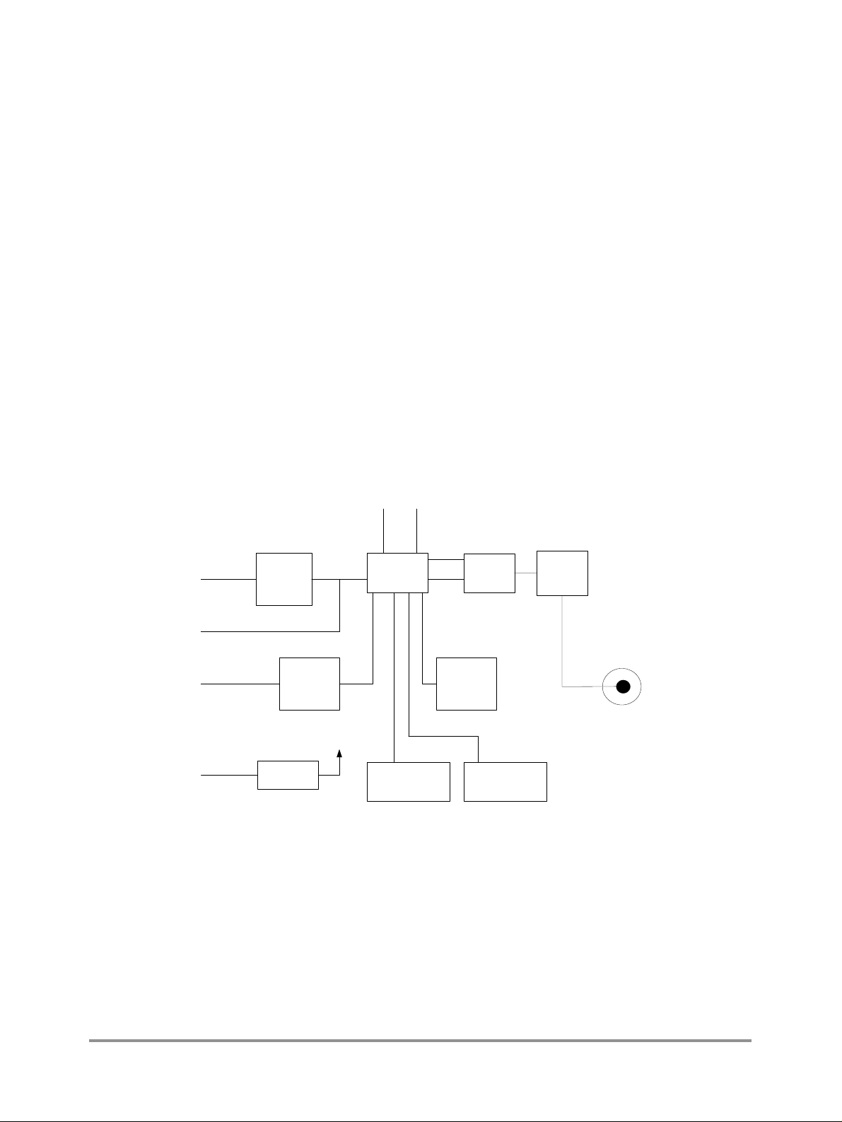
2.1 Block Diagram
The following figure shows the 72000 Development Kit block diagram:
Figure 2-1. Block Diagram
32 KHz
RS232
UART
Modular Jack
RS232
Level
Shifter
CODEC
13 MHz
MC72000
Rx
Rx/Tx
Tx
Switch
EEPROM
Band
Pass
Filter
Antenna
Connector
DC
Power
Input
MC13181
Status LEDs Reset Switch
MOTOROLA Product Overview 2-5
Preliminary
Page 10

Product Overview
2.2 Interfaces
The 72000 Development Kit features the following interfaces:
• RS232 interface: Programmable baud rate from 1200 to 921 Kbit.
• UART interface: 5-pin header with RxD, CTS, RTS, and GND, 3.3 V signaling, programmable
baud rate from 1200 to 921 Kbit, HCI UART transport layer.
NOTE:
The UART and RS232 interfaces cannot operate simultaneously.
• Audio connections, with audio routed to the CODEC.
2.3 ICs
The 72000 Development Kit is supplied with the following Bluetooth ICs from Motorola:
• MC72000 Bluetooth Baseband Controller and Transceiver IC
• MC13181 Wireless Power Management IC
The 72000 Development Kit uses an Atmel SEEPROM (AT25HP512).
2.4 Software Tools
The 72000 Development Kit is accompanied by the following software tools:
• Bluetooth HCI Terminal
• Configuration manager
• DemoBench
• RadioTest
The following sections describe briefly each of the software tools. A separate user’s guide for each tool is
included on the Development Kit CD.
2.4.1 Bluetooth HCI Terminal
With the Bluetooth HCI Terminal you can interact with your Bluetooth hardware. The interface is similar
to that of an AT Terminal application when communicating with a modem. The Bluetooth HCI Terminal
makes it easy to send HCI commands from a computer to a Bluetooth device. Likewise, it is easy to
receive HCI responses from a Bluetooth device. Consequently, you can get hands-on experience with the
HCI. Or you can test your own Bluetooth hardware.
2.4.2 Configuration Manager
The Configuration Manager is an application that allows you to handle the Development Kit file system.
With this tool, you can download firmware patches and set up a number of baseband and radio parameters
to exercise the board. All parameters are restorable and default settings are stored automatically.
2-6 72000 Development Kit User’s Guide MOTOROLA
Preliminary
Page 11

Software Tools
2.4.3 DemoBench
The DemoBench is a demonstration tool that can be used for a number of purposes. You can send a file to
another Bluetooth device, “chat” with another Bluetooth device, and view link and packet statistics in a
real-time application.
2.4.4 RadioTest
The RadioTest application allows you to test all aspects of your Bluetooth hardware. This application lets
you control your hardware so as to carry out any test required for development purposes and when
preparing for production. Testing is both fast and simple; you can do all your testing with one and the same
program. In addition, you can create your own test system as desired without losing any of the benefits of
the Radio Test application. Finally, the application allows for simultaneous testing of several units using
the same equipment.
MOTOROLA Product Overview 2-7
Preliminary
Page 12

Product Overview
2-8 72000 Development Kit User’s Guide MOTOROLA
Preliminary
Page 13

Chapter 3
Setup
This section explains how to set up the 72000 Development Kit hardware and software. Do the following:
1. Attach external antenna to the 50 ohm connector on the development board.
2. Attach the development board to your computer using the UART (RS232) cable.
3. Attach power supply to DC connector on board and connect to main electricity supply.
4. Insert the CD in the CD-ROM drive of your computer and follow the o nscreen instructions
to install the software and documentation.
5. Launch the Configuration Manager and make sure it is the only Development Kit
application running.
6. Select the "72000 - UART Application - Audio through Codec" configuration in the
Configuration Manager and click the Make Active button.
You can now use UART or RS232, however not simultaneously.
NOTE:
The first time the Configuration Manager is attached to a board, it will
advise you to make a backup of the configuration on the board. A backup
is necessary to save the board’s original settings. The backup will be called
Factory Settings for device XXXXXXXXXXXX.
MOTOROLA Setup 3-9
Preliminary
Page 14

Setup
3-10 72000 Development Kit User’s Guide MOTOROLA
Preliminary
Page 15

Chapter 4
Hardware
This section provides information on various aspects of the 72000 Development Kit hardware. In addition,
Appendix A, “Board Diagrams“, contains the development board schematic and component placement,
and Appendix B, “Bill of Material“, contains the BOM.
4.1 Signal and Connection Descriptions
The 72000 Development Kit contains the following connections, switches, and indicators:
• Power supply input
• Modular jack 4/4 connector for mono-audio speaker and microphone (headset application)
• RS232 interface
• UART interface
• Antenna connector
• JTAG allowing interface to MC72000 production test
• Reset button
• Three control buttons for future applications
• On/off switch
• Status LEDs
• Software download switch
The power supplied for the 72000 Development Kit is DC with the ratings stated in the specifications.
An analog audio signal to be transmitted over the Bluetooth connection can be fed into the 72000
Development Kit via the modular jack or as streaming audio through the host interface. It will be converted
to digital data and transmitted through the Bluetooth link. A digital audio signal received from a connected
Bluetooth device will be converted to an analog audio signal and available at the modular jack or as
streaming audio through the host interface (UAR T, SSI, SPI). The MC72000 has a Blu etooth Audio Sign al
Processor (BTASP) for superior audio performance.
The RS232/UART interfaces can be used to transfer data and audio between a host and the Bluetooth device.
The firmware of the 72000 Development Kit can be upgraded through the RS232/UART interface.
The CODEC is attached to the MC72000 via SSI interface.
The antenna connector is an SMA 50 ohm connection.
The reset button can be activated to re-initialize the entire system.
MOTOROLA Hardware 4-11
Preliminary
Page 16

Hardware
Three buttons are provided for future embedded applications.
Four status LEDs are provided:
• One application-specific LED
• 24 MHz/32 kHz
•RX/TX
•Power on
4.2 Environmental
This section contains system level environmental information about the development board::
• Storage temperature (degrees centigrade):
—Min. -40
—Max +125
• Operating temperature (degrees centigrade):
—Min. 0
—Max +85
4.3 Mechanical
This section contains system level mechanical information:
• Length: 75mm
• Width: 50 mm
• Height (PCB with components):
— Excluding legs: 18 mm
— Including legs: 25 mm
• Layout, FR4, 4 layer: 1 mm
4.4 Electrical
This section contains electrical information:
• Input power supply requirements: 3.5-6.5 VDC
• Audio input: 65m Vpp
• Audio output: 1.6 Vpp, modular jack 4/4 connector
4-12 72000 Development Kit User’s Guide MOTOROLA
Preliminary
Page 17

Electrical
The following table shows the current consumption measurements of the circuits of the MC72000
Bluetooth Baseband Controller and Transceiver IC.
Table 1: Current Consumption Measurements of MC72000
Type
DH5 asymmetric
RX
DH5 asymmetric TX55.5 mA TX rate 723.2 kbits
DH5 symmetric 57.5 mA TX rate 433.9 kbits
HV1 54.8 mA
HV3 TDB
Total system in
low-power mode
Average
Current
57 mA TX rate 57.6 kbits
RX rate 723.2 kbits
RX rate 57.6 kbits
RX rate 433.9 kbits
TDB
Note that the table contains typical values.
4.4.1 Power Supply
The board is fed with power from on-board standard regulators.
Description
The on-board power supply regulators should be fed with the supply provided, which generates the
following voltages for the board:
•1.85 V
•2.65 V
•3.0V
4.4.2 Reset Circuit
The board includes a push button for full system reset of the MC72000 and all peripherals.
4.4.3 Clocks
The clocks in the system are as follows:
• External crystal: 13 MHz
• Sleep mode clock: 32.768 kHz
• Active mode clock: 24 MHz
The MC72000 includes an internal oscillator circuit for the 32.768 kHz sleep mode clock and the 24 MHz
active mode clock. Only two external crystals and a few other components are needed.
MOTOROLA Hardware 4-13
Preliminary
Page 18

Hardware
4.4.4 Memory
The MC72000 has embedded memory of 256 Kbytes of ROM and 64 K of RAM. The file system and
application can be uploaded from a host system, or a low-cost serial EEPROM (four-wire connection). For
more information on the contents and structure of the MC72000 memory, please refer to the Bluetooth
Platform Solution Embedded System User’s Guide. This is accessible from the document overview on the
Development Kit CD.
4.4.5 UART Interface
The UART interface is embedded in the MC72000. However, an external level converter is needed. For
this purpose, the MAX3237 1.0 Mbit level converter is used. The level converter is connected to the
MC72000 and a female 9-pin D-sub. The connection between the level converter and the MC72000 is
passed through a jumper block in order to aid debugging, and, if ever needed, to use a different type of
level converter.
4.4.6 CODEC Interface
The audio interface consists of the Motorola MC145483 CODEC, a 4-pin header and a 4/4p amp
connector. Sampling rate is configured at 7.8125 kHz.
4.4.6.1 Codec Setup and Configuration
In the current (Motorola CODEC) configuration for the 72000 Development Kit, the CODEC can only be
configured as a slave, which is done by the application at startup. Therefore, the MC72000 IC will be
configured as the SSI master, meaning that the MC72000 IC generates all SSI control signals. In practice,
the CODEC bit clock is tied electrically to the master clock.
There are certain constraints on the available clock frequencies; specifically, the frequency can only be
integer factors of the baseband’s master clock, which is 24 MHz. The Motorola CODEC expects a 2.048
MHz master clock, but due to these limitations, none of the available integral frequencies fit the CODEC
exactly. Therefore, a slight mismatch in the order of two per cent exists. To be exact, the CODEC expects
a 2.048 MHz master clock, but gets 2.000 MHz.
The frame sync generated by the MC72000 IC can only by an integer factor of the master clock (bit clock),
and is selected as 1/256th, resulting in:
• Frame sync: 2000 kHz / 256 = 7.8125 kHz
This slight mismatch does not cause any audio degredation. Interpolation copes with the synchronization
seamlessly. The degradation of the frequency characteristic of the system from runnning on a slightly
lower sample frequency is not significant. (The pass-band upper frequency is 3.9 kHz instead of 4.0 kHz).
Figure 4-1. SSI Signals from Baseband to CODEC
STXD
SRXD
STCK
STFS
Motorola CODEC
4-14 72000 Development Kit User’s Guide MOTOROLA
Preliminary
Page 19

Electrical
4.4.7 Antenna
The 72000 Development Kit contains an SMA 50 ohm antenna connector.
4.4.8 100 mm² Module
A six-layer HDI PCB with an area of 100mm² has been populated with an MC72000 IC and all the
necessary external components for a host-based solution, where the reference oscillator signals are
provided by the host. This serves as a demonstration of the space efficiency of the MC72000 Bluetooth
solution. This PCB has been fitted with pads to resemble a QFN package and has been mounted on the
motherboard.
For a diagram of this module, see Appendix C, “100 mm² Module Diagram“.
MOTOROLA Hardware 4-15
Preliminary
Page 20

Hardware
4-16 72000 Development Kit User’s Guide MOTOROLA
Preliminary
Page 21

Chapter 5
Regulatory
This section contains regulatory statements, a list of the countries where the 72000 Development Kit has
obtained type approval or may be shipped as a prototype, and information on wh at is needed by developers
to obtain type approval for their products.
NOTE:
This device is intended for evaluation and development purposes by
professionals only and is NOT for re-sale.
5.1 Regulatory Statements
This section contains the regulatory statements that apply to the 72000 Development Kit.
NOTE:
Users are not permitted to make changes or modify the system in any way .
Changes or modifications not expressly approved by the party responsible
for compliance could void the user’s authority to operate the equipment.
5.1.1 General
This product complies with any mandatory product specification in any co unt ry wh ere th e product is sold.
5.1.2 European Union (EU) and EFTA
This equipment complies with the R&TTE directive 1999/5/EC and has been provided with the CE mark
accordingly.
5.1.3 France
This equipment may only be used as a Class 2 device, not as a Class 1 device. Note also that only indoor
use is allowed.
MOTOROLA Regulatory 5-17
Preliminary
Page 22

Regulatory
5.1.4 United States of America and Canada
Tested to comply with FCC Standards FOR HOME OR OFFICE USE. See FCC 47CFR part 15.19(b)(2)
This device complies with part 15 of the FCC rules and with RSS-210 / RSS-139 of the Industry Canada.
Operation is subject to the following two conditions: (1) This device may not cause harmful interference,
and (2) this device must accept any interference received, including interference that may cause undesired
operation. See FCC regulation CFR47 sec. 15.19(3).
This equipment has been tested and found to comply with the limits for a Class B digital device, pursuant
to part 15 of the FCC Rules. These limits are designed to provide reasonable protection against harmful
interference in a residential installation. This equipment generates, uses and can radiate radio frequency
energy and, if not installed and used in accordance with the instructions, may cause harmful interference to
radio communications. However, there is no guarantee that interference will not occur in a particular
installation. If this equipment does cause harmful interference to radio or television reception, which can
be determined by turning the equipment off and on, the user is encouraged to try to correct the interference
by one or more of the following measures:
• Reorient or relocate the receiving antenna
• Increase the separation between the equipment and receiver
• Connect the equipment into an outlet on a circuit different from that to which the receiver is
connected
• Consult the dealer or an experienced radio/TV technician for help
In order to comply with FCC RF Exposure requirements, a minimum separation distance of 20 cm must
always be maintained between the transmitter antenna and all persons during normal operation.
Note that any changes or modifications to this equipment not expressly approved by the manufacturer may
void the FCC authorization to operate this equipment. See FCC regulation CFR47 sec. 15.21.
5.1.5 Canada Compliance (Industry Canada)
To prevent radio interference to the licensed service, this device is intended to be operated indoors
and away from windows to provide maximum shielding. Equipment that is installed outdoors is
subject to licensing.
In French: Pour empêcher un brouillage radioélectrique au service faisant l'objet d'une licence, cet
appareil doit être utilisé à l'interieur et loin des fenêtres afin de founir un écran de blindage
maximal. Au cas aù un installation en plain air, le materiel doit faire l'objet d'une licence.
This device has been designed to operate with an antenna having a maximum gain of 5.00 dBi. Antenna
having a higher gain is strictly prohibited per regulations of Industry Canada. The required antenna
impedance is 50 ohms.
To reduce potential radio interference to other users, the antenna type and its gain should be so chosen that
the equivalent isotropically radiated power (EIRP) is not more than that required for successful
communication.
The term "IC:" before the radio certification number only signifies that Industry Canada technical
specifications were met.
5-18 72000 Development Kit User’s Guide MOTOROLA
Preliminary
Page 23

5.1.6 Taiwan
Development Kit Approval
5.2 Development Kit Approval
5.2.1 Type Approval
In the following countries, the 72000 Development Kit has obtained type approval:
• Europe (EU and EFTA countries)
•USA
• Canada
• Japan*
* The equipment will be tested at accredited in-country test house. However, actual application will not be submitted as the 72000
development board has no enclosure, which is requested for approval in Japan.
MOTOROLA Regulatory 5-19
Preliminary
Page 24

Regulatory
5.2.2 Prototype Shipment
In the following countries, the 72000 Development Kit has not been typed approved but prototypes may be
shipped:
• China
•Taiwan
• Israel**
• Hong Kong
• Korea (South)
• Singapore
•Brazil
•Mexico**
** Awaiting new regulations.
5.3 Obtaining Type Approval
Customers of Motorola Bluetooth chipsets will face some Bluetooth qualification and regulatory
requirements for their products. The following lists the requirements for the major markets as defined by
Motorola as tier 1 countries: Australia, Canada, Europe (15 + 4 EFTA countries), Japan, New Zealand and
the US. A number of other countries worldwide will accept the test reports made for Europe and/or US
approval; for more information, please go to: http://www.bluetooth.org/member/regulatory.
Motorola chipsets (radio/baseband) are pre-qualified as Bluetooth components; for more information,
please go to: http://qualweb.opengroup.org/Template2.cfm?LinkQualified=QualifiedProducts. Also any
variants of Motorola software stacks will be pre-qualified. The assumption of pre-qualification provides
that customers will implement the radio module (radio chip including surrounding components and print
layout) without any changes.
5.3.1 Requirements for Bluetooth Qualification
Baseband chipset will be used as a pre-qualified component and do not require re-testing.
Any incorporated variant of Motorola software stack will be used as a pre-qualified component and do not
require re-testing.
Radio will need to be re-tested in the product layout for the 8 (of 16) test cases listed in the following table.
(For more information, see “The Bluetooth Qualification Program Reference Document (BQ PRD)” on the
Bluetooth Qualification Program Website: http://qualweb.bluetooth.org/Template2.cfm.)
5-20 72000 Development Kit User’s Guide MOTOROLA
Preliminary
Page 25

Obtaining Type Approval
Table 5-1.
TRM/CA/04/E TX Output Spectrum-Frequency range
TRM/CA/08/E Initial Carrier Frequency Tolerance
TRM/CA/09/E Carrier Frequency Drift
TTRC/CA/01/E Out-of-Band Spurious Emissions-radiated
RCV/CA/02/E Sensitivity-multi-slot packets
RCV/CA/03/E C/I performance
RCV/CA/04E Blocking performance
TP/PHYS/TRX/BV-05-C Symbol rate
If changes are made to the 72000 Development Kit radio module BOM or layout, all 16 Bluetooth test
cases will be required to be re-tested. Depending on the nature of changes to the radio, re-testing might
only be necessary in normal temperature. This has to be decided by the BQB in each case.
5.3.2 Requirements for Regulatory Type Approval
The following regulatory testing needs to be made:
• For CE-marking: EN 300 328-2 (emission), EN 301 489-17 (EMC), EN 60950 (safety)
• For Japan approval: ARIB T-66.
• For FCC grant: CFR47 part 15.205, 15.209 and 15.247 (except 15.247e: processing gain)
NOTE:
As Motorola radios will be approved by FCC as radio modules and the
FCC testing can be avoided for regulatory purposes for radio modules,
provided no changes are made to the radio module BOM or layout, it will
still be necessary to perform the Out-of-Band Spurious
Emissions-radiated-test of part 15.209.
The product might be subject to additional product specific regulations, such as PSTN regulations and
other.
Type approval applications have to be filed to the national authorities for each product.
Documentation submitted for type approval can vary from country to country, but will in general include:
test reports, pictures, BOM, schematics, PCB layouts, product descriptions (block diagrams), antenna
information, SAR statements (see below), label/manual information (legal text) and manufacturer
information.
Both in Europe and US regulators are currently working on new sets of rules for combined radio
equipment as well as rules for SAR. Test requirements for SAR (including combined radio) will most
likely be topical within the next year.
MOTOROLA Regulatory 5-21
Preliminary
Page 26

Regulatory
5-22 72000 Development Kit User’s Guide MOTOROLA
Preliminary
Page 27

Appendix A
Board Diagrams
The following pages show the 72000 development board schematic and component placement.
MOTOROLA A-1
Preliminary
Page 28

C C
JTAG
Secundary fiducial point (Soldside)
A3
A A
Secundary fiducial point (Compside)
Primus datum point (Compside)
A2
A1
B B
4- 6VDC
JTAG0
JTAG3
5
PCB Corner Mark
np hole ø4.2mm
PCB Corner Mark
CO2
CO1
HOLE1
np hole ø4.2mm
HOLE2
CO3
PCB Corner Mark
CO4
PCB Corner Mark
HOLE3
np hole ø4.2mm
HOLE4
np hole ø4.2mm
DIG504-2
4
PCB101
JTAG4 JTAG2
Not Mounted
RESET
UART[0..3]
VDD1V85
1 2
3 4
5 6
7 8
J103
109
JTAG6
JTAG1
GPIO[0..3]
SSI[0..3]
D D
Power Supply
DC
321
4
MAIN+
JTAG[0..6]
J101
5
4
3
2
Date: Sheet
1
Title
Size Document Number
Digianswer A/S
Skalhuse 5
DK-9240 Nibe, Denmark
Telephone: +45 96710000 Fax: +45 98350052 http://www.digianswer.com
A3
MC72000 Development kit (DIG504-2) : Main schematic
80000504000_R0200.DSN R02.00
© Digi answer
Module Peripherals
2
A15C2
Co nf i de nt i a l Inf orm ati on
This document contains Digianswer A/S confidential and proprietary information, which you are not
entitled to reproduce or disclose to any third party without the prior written consent of Digianswer A/S.
1
C4
C33A2
4
6
C1
IC101
MMQA5V6T1
Sheet3
REFCTRL
UART[0..3] BT_WAKEUP
SSI[0..3]
GPIO[0..3]
CLK0
CLK1
EPADRV
RESET
Power_ON
Speak+
Speak-
MIC+
MIC-
MIC-
MIC+
EAR-
EAR+
4
J105
4/4p
1122334
RXD
CTS
RTS
TXD
Ri
R103 0R
R101 0R
R102
Not Mounted
0R
CTS
TXD
RXD
RTS
594837261
m1 m2
9p Female Ang
UAR T
J104
Module and Power
Not Mounted
J107
UART[0..3]
SSI[0..3]
GPIO[0..3]
CLK0
CLK1
Not Mounted
J106
EPADRV
Power_ON 13MHz_osc
1
253
4
SMA Receptacle, Female
RESET
J102
4
13M Hz osc illat or
REFCTRL
32kHz_osc
1
253
4
32k Hz osc illat or
ANT ENNA
Sheet 2
MAIN+
JTAG[0..6] Antenna
3
RFNET2
1
253
2
1
14Thursday, August 01, 2002 CLL
of
Rev
A-2 72000 Development Kit User’s Guide MOTOROLA
Preliminary
2002
Page 29

A A
B B
C C
D D
MAIN+
5
4
3
2
Size Document Number
Date: Sheet
A3
MC72000 Development kit (DIG504-2) : Module and Power
80000504000_R0200.DSN R02.00
1
Title
Co nf i de nt i a l Inf orm ati on
Digianswer A/S
This document contains Digianswer A/S confidential and proprietary information, which you are not
entitled to reproduce or disclose to any third party without the prior written consent of Digianswer A/S.
Skalhuse 5
DK-9240 Nibe, Denmark
Telephone: +45 96710000 Fax: +45 98350052 http://www.digianswer.com
© Digi answer
10K
63
68
48
100mm2 Pillaris Daughter board
GND264GND1
GNDcore_I2
GNDDEMO
GNDMOD
GNDVCO
GNDPRE
GNDCP
VSS_2
9
7
14
18
16
R216
GND_IO6GNDpb_pc53GND_EIM13GNDcore_I1
GNDLNA1
20
35
Switch
JTAG[0..6]
GNDPA
24
AT25HP512-10CI-1.8
123
2*5p
JTAG4
JTAG6
JTAG5
31
GND337GND6
GND534GND4
39
S201
JTAG3
109
JTAG2
33
100nF
5
1 2
1.0K
1
324
R202
BZV90C6V8
TP201
R210
Not Mounted
R209
C215
100nF
4
WP3GND
SO
SI
5
470R
7 8
SPI13
JTAG1
TRST27TDI28TDO30TMS26RTCK25TTS29TCK
VCCDC
C216
HOLD7VCC
SCK
2
6
R215
3 4
5 6
SPI10
SPI12
JTAG0
VCCVCO
32
17
C214
100nF
8
CS
1
1 2
J201
SPI11
GPIO[0..3]
GPIO1
GPIO2
60
58
GPIO_C9
VCCMOD
VCCCP
8
19
C213
100nF
IC202
GPIO3
VDD_1
10
10K
C211
GPIO0
OSC32k59GPIO_B1050GPIO_B12
VCCDEMO
VCCPRE
15
36
C212
100nF
R214
10pF
10M
Not Mounted
VCCLNA
VCCPA
21
23
100nF
VDD3V
10pF
X201
32.768KHz
10M
R213
R212
100K
R219
0R
R220
TP205
REFCTRL
41
40
11
XTAL
EXTAL
REFCTRL
EPADRV
NC
42
22
VCC_RF
EPADRV
C210
0R
14
13
MC13181
2V65_ENABLE171V85_ENABLE
3V0/3V3 sel
3V0/3V3 ENABLE
AGND2
SGND
EP
5
EP
20
C206
1µF
32kHz_osc
C209
C221
Not Mounted
R211
SPI13
SPI12
SPI11
SPI10
UART1
UART2
UART3
2
3
5
SPI1-MISO
SPI1-SCK4SPI1-SS
BASEBAND
XEMIT
46
R218
0R
C207
15pF
C208
15pF
18
AGND1
4
1µF
UART0
TxD62RxD57CTS61RTS56SPI1-MOSI
XBASE
C205
UART[0..3]
45
R217 0R
R207
0R
12
Q1_b10S INV6Q211S OR
Shutdown
OUT3V0/3V3
OUT2V651OUT1V8519RESET_b
7
R208
1.5R
R205
1.5R
VDD3V
R206
0.47R
VCC_RF
C204
1µF
SSI0
SSI1
SSI2
SSI3
51
49
54
SSI_STCK_SRCK
SSI_STFS_SRFS
SSI_STD55SSI_SRD
CLK0
RADIO
VCCXTAL
44
VCC_RF
Not Mounted
C222
X202
13.000MHz
13MHz_osc
21
16
3
8
VCC1
Vin+24Vin-23HysteresisSelect
VCC2
DelayCap
REFOUT
Detect
15
22
2
9
C202
100nF
C203
100nF
R204 1.0K
VDD1V85
RESET
SSI[0..3]
C219
100nF
CLK0
CLK1
100nF
C220
43
65
52
1
RESET
CLK166VDDpb_pc
VDD_EIM12VDD_IO
VCC
IC201
RESET
VDD3V
100nF
100nF
47
VDDcore_I2
C218
C217
67
CON201
VDDcore_I1
For DIG499-2 and DIG501-2
Antenna
38
RFNET1
Antenna
VDD1V85
R201
500mA
D201
100µF
C201
Green LED
D202
1
2
3
J202
1p
J203
1p
J204
1p
VDD1V85
J205
1p
VCC_RF VDD3V
J206
1p
S202
Switch
VCC
Z0=50ohm Track 523µm, layer 1-2 300µm
4
3
2
1
24Thursday, August 01, 2002 CLL
of
Rev
MOTOROLA A-3
Preliminary
2002
Page 30

A A
CLK1
SSI[0..3]
B B
C C
D D
24MHz / 32kHz
13
MAX3237EAI
EN
MBAUD
SHDN
14
15
TP317
TP309
R312
10K
10K
TP310
10K
2*6p
18
R3OUT
R3IN
11
Ri
R311
UART[0..3]
20
9
RXD
R310
R1OUT21R2OUT
R1IN8R2IN
RTS
UART[0..3]
UART1
11 12
9 10
16
R1OUTB
2
34
BC847BS
5
61
BC847BS
2
UART3
UART2
5 6
7 8
17
12
Level shifter
61
TR301A
BC847BS
TR301B
TR302A
UART0
1 2
3 4
J301
23
T1IN24T2IN
T3IN22T4IN19T5IN
T1OUT5T2OUT
T3OUT7T4OUT10T5OUT
6
TXD
BT_WAKEUP
CTS
TP306
R305
470R
R306
470R
TP307
Red/Green LED SMD
R
2
G
4 3
TP308
5
VDD3V
C301
100nF
C305
100nF
D303
470R
3
GND
2
100nF
Red LED
Green LED
1
R304
D301
D302
TP302
IC301
C1+28C1-25C2+1C2-
VCC
V+
V-
26
27
4
100nF
C302
C304
C303
100nF
R301
0R
R303
470R
4
3
2
GPIO[0..3]
5
C313
100nF
4
C315
100nF
C316
100nF
270K
C314
330nF
3
220R
C310
1µF
1.0K
2
R325
2.2K
R322
R321
VAG
MIC+
15
MC145483SD
VSS
VAG-Ref
1
R324
C312
150pF
C311
330nF
R323
2.2K
MIC-
VDD3V
16
6
VDD
HB
VAG
TI+
TG
TI-
20
18
19
VAG
270K
R326
1.0K
SSI0
SSI1
SSI2
SSI3
11 12
1 2
3 4
5 6
7 8
9 10
2*6p
GPIO3
0R
R331
R330
0R
11
10
PDI
PO+
17
5
TP316
R320
C309
150pF
C317
1µF
LM4878
100nF
J302
Not Mounted
R328
14
9
FSR7DR
BCLKR
DT13FST
BCLKT12MCLK
RO-
PO-
PI
3
4
R318
10K
R319
10K
22nF
43K
5
-IN1+IN7Bypass3Shutdown
OUT 18OUT 2
GND
VDD
2
4
C308
Speak+
Speak-
VDD3V
R327
0R
8
IC302
2
C307
R317
IC303
6
VCC
C306
1.0nF
R316
43K
TP315
CLK0
REFCTRLEPADRV
Title
Size Document Number
Date: Sheet
A3
MC72000 Development kit (DIG504-2) : Module peripherals
80000504000_R0200.DSN R02.00
1
34Thursday, August 01, 2002 CLL
of
Rev
Co nf i de nt i a l Inf orm ati on
Digianswer A/S
This document contains Digianswer A/S confidential and proprietary information, which you are not
entitled to reproduce or disclose to any third party without the prior written consent of Digianswer A/S.
Skalhuse 5
DK-9240 Nibe, Denmark
Telephone: +45 96710000 Fax: +45 98350052 http://www.digianswer.com
© Digi answer
2002
SPST
S304
TP318
VDD3VVDD3V
R302
0R
GPIO[0..3]
GPIO2
GPIO0
GPIO1
TP303
TP304
TP305
SPST
SPST
SPST
S301
S302
S303
Keys
Vol +Vol - BT
1
R307
R313
100R
RESET
10K
R308
10K
R309
10K
A-4 72000 Development Kit User’s Guide MOTOROLA
Preliminary
Page 31

Physical Layer 1
MOTOROLA A-5
Preliminary
Page 32

Physical Layer 2
A-6 72000 Development Kit User’s Guide MOTOROLA
Preliminary
Page 33

Appendix B
Bill of Material
This appendix shows the Bill of Material for the 72000 Development Kit PIN 80000504000 Rev. R02.00.
Table B-1.
Item Value Rating Tolerance Manufacturer
1 100µF 10V 20% AVX TPSD107MOlOR0150 C201
2 100nF 6.3V 10% X513 Murata GRP155R60J104KA01E C202
3 100nF 6.3V 10% X513 Murata GRP155R60J104KA01E C203
4 100nF 6.3V 10% X513 Murata GRP155R60J104KA01E C210
5 100nF 6.3V 10% X513 Murata GRP155R60J104KA01E C212
6 100nF 6.3V 10% X513 Murata GRP155R60J104KA01E C213
7 100nF 6.3V 10% X513 Murata GRP155R60J104KA01E C214
8 100nF 6.3V 10% X513 Murata GRP155R60J104KA01E C215
9 100nF 6.3V 10% X513 Murata GRP155R60J104KA01E C216
10 100nF 6.3V 10% X513 Murata GRP155R60J104KA01E C217
11 100nF 6.3V 10% X513 Murata GRP155R60J104KA01E C218
12 100nF 6.3V 10% X513 Murata GRP155R60J104KA01E C219
13 100nF 6.3V 10% X513 Murata GRP155R60J104KA01E C220
Manufacturer's Part
Number
Part
Reference
14 100nF 6.3V 10% X513 Murata GRP155R60J104KA01E C301
15 100nF 6.3V 10% X513 Murata GRP155R60J104KA01E C302
16 100nF 6.3V 10% X513 Murata GRP155R60J104KA01E C303
17 100nF 6.3V 10% X513 Murata GRP155R60J104KA01E C304
18 100nF 6.3V 10% X513 Murata GRP155R60J104KA01E C305
19 100nF 6.3V 10% X513 Murata GRP155R60J104KA01E C308
20 100nF 6.3V 10% X513 Murata GRP155R60J104KA01E C313
21 100nF 6.3V 10% X513 Murata GRP155R60J104KA01E C315
MOTOROLA B-1
Preliminary
Page 34

Table B-1.
Item Value Rating Tolerance Manufacturer
22 100nF 6.3V 10% X513 Murata GRP155R60J104KA01E C316
23 1µF 6.3V 10% X513 Murata GRM188R60J105K C204
24 1µF 6.3V 10% X513 Murata GRM188R60J105K C205
25 1µF 6.3V 10% X513 Murata GRM188R60J105K C206
26 1uF 6.3V 10% X513 Murata GRM188R60J105K C310
27 1uF 6.3V 10% X513 Murata GRM188R60J105K C317
28 15pF 50V 5% NPO Murata GRM36COG15OJ50PT C207
29 15pF 50V 5% NPO Murata GRM36COG15OJ50PT C208
30 10pF 50V 5% NPO Murata GRM36COGlOOD50PT C209
31 10pF 50V 5% NPO Murata GRM36COGlOOD50PT C211
32 1.0nF 50V 5% X713 Murata GRM36X7R102K50PT263 C306
33 22nF 16V 10% X713 AVX-Kyocera 0402YC223KAT2A C307
34 150pF 50V 5% X713 Murata GRM36COG151J50PT263 C309
Manufacturer's Part
Number
Part
Reference
35 150pF 50V 5% X713 Murata GRM36COG151J50PT263 C312
36 330nF 6.3V 10% X513 AVX-Kyocera 06036D334KAT2A C311
37 330nF 6.3V 10% X513 AVX-Kyocera 06036D334KAT2A C314
38 100mm2
daughter
board
39 BZV90C6V8 Philips BZV90C6V8 D201
40 Green LED Citizen CL-170G-CD-T D202
41 Green LED Citizen CL-170G-CD-T D302
42 Red LED Citizen CL-170R-CD-T D301
43 Red/Green
LED SMD
44 MMQA5V6T1 5.6V/24W Motorola MMQA5V6T1 IC101
45 MC13181 Motorola PC13181 IC201
46 AT25HP512-
10CI-1.8
Digianswer 80000501000 CON201
Kingsbright
Electronic
ATMEL AT25HP512-10CI-1.8 IC202
KPB-3025ESGC D303
47 MAX3237EAI MAXIM MAX3237EAI IC301
B-2 72000 Development Kit User’s Guide MOTOROLA
Preliminary
Page 35

Table B-1.
Item Value Rating Tolerance Manufacturer
48 MC145483S
D
49 LM4878 NATIONAL LM48781BP IC303
50 DC Roka 5202550 1101
51 SMA Recep-
tacle, Female
52 9p Female
Ang
53 4/4p AMP 215875-1 J105
54 2*5p AMP 826632-5 J201
55 1p AMP 826629-1 J202
56 1p AMP 826629-1 J203
57 1p AMP 826629-1 J204
58 1p AMP 826629-1 J205
Motorola MC145483SD IC302
Telegärtner J01151AO931 J102
AMP 747844-5 J104
Manufacturer's Part
Number
Part
Reference
59 1p AMP 826629-1 J206
60 2*6p AMP 1-826632-2 J301
61 2*6p AMP 1-826632-2 J302
62 DIG504-2 PCB101
63 OR 62.5mW/5
0V
64 OR 62.5mW/5
0V
65 OR 62.5mW/5
0V
66 OR 62.5mW/5
0V
67 OR 62.5mW/5
0V
68 OR 62.5mW/5
0V
69 OR 62.5mW/5
0V
5 % Phycomp 2322 705 91001 R101
5 % Phycomp 2322 705 91001 R103
5 % Phycomp 2322 705 91001 R207
5 % Phycomp 2322 705 91001 R209
5 % Phycomp 2322 705 91001 R217
5 % Phycomp 2322 705 91001 R218
5 % Phycomp 2322 705 91001 R219
70 OR 62.5mW/5
0V
5 % Phycomp 2322 705 91001 R301
MOTOROLA B-3
Preliminary
Page 36

Table B-1.
Item Value Rating Tolerance Manufacturer
71 OR 62.5mW/5
0V
72 OR 62.5mW/5
0V
73 OR 62.5mW/5
0V
74 OR 62.5mW/5
0V
75 500mA Raychem microSMD050-2 R201
76 1.0K 62.5mW/5
0V
77 1.0K 62.5mW/5
0V
78 1.0K 62.5mW/5
0V
79 1.0K 62.5mW/5
0V
5 % Phycomp 2322 705 91001 R302
5 % Phycomp 2322 705 91001 R327
5 % Phycomp 2322 705 91001 R330
5 % Phycomp 2322 705 91001 R331
1 % ROHM M CR01MZSF1001 13202
1 % ROHM M CR01MZSF1001 13204
1 % ROHM M CR01MZSF1001 13321
1 % ROHM M CR01MZSF1001 13326
Manufacturer's Part
Number
Part
Reference
80 1.513 100mW/5
0V
81 1.513 100mW/5
0V
82 0.4713 100mW/1
50V
83 100K 62.5mW/2
5V
84 10M 100mW/5
0V
85 10M 100mW/5
0V
86 10K 62.5mW/2
5V
87 10K 62.5mW/2
5V
88 10K 62.5mW/2
5V
89 10K 62.5mW/2
5V
1% Phycomp 2322 704 61508 13205
1% Phycomp 2322 704 61508 13208
5 % KOA Speer
Electronics Inc.
5% YAGEO RC02104JR 13211
5% YAGEO RC0603JRF0710M 13212
5% YAGEO RC0603JRF0710M 13213
5% YAGEO RC02103JR 13214
5% YAGEO RC02103JR 13216
5% YAGEO RC02103JR 13307
5% YAGEO RC02103JR 13308
SR73K2ATDJ OE47 13206
B-4 72000 Development Kit User’s Guide MOTOROLA
Preliminary
Page 37

Table B-1.
Item Value Rating Tolerance Manufacturer
90 10K 62.5mW/2
5V
91 10K 62.5mW/2
5V
92 10K 62.5mW/2
5V
93 10K 62.5mW/2
5V
94 10K 62.5mW/2
5V
95 10K 62.5mW/2
5V
96 47013 63mW/50
V
97 47013 63mW/50
V
5% YAGEO RC02103JR 13309
5% YAGEO RC02103JR 13310
5% YAGEO RC02103JR 13311
5% YAGEO RC02103JR 13312
5% YAGEO RC02103JR 13318
5% YAGEO RC02103JR 13319
5 % KOA Speer
Electronics Inc.
5 % KOA Speer
Electronics Inc.
Manufacturer's Part
Number
RK73B1 ETP470J 13215
RK73B1 ETP470J 13303
Part
Reference
98 47013 63mW/50
V
99 47013 63mW/50
V
100 47013 63mW/50
V
101 10013 62.5mW/2
5V
102 43K 62.5mW/5
0V
103 43K 62.5mW/5
0V
104 270K 62.5mW/5
0V
105 270K 62.5mW/5
0V
106 22013 62.5mW/2
5V
107 2.2K 62.5mW/5
0V
5 % KOA Speer
Electronics Inc.
5 % KOA Speer
Electronics Inc.
5 % KOA Speer
Electronics Inc.
5% YAGEO RC02101JR 13313
1 % ROHM M CR01MZSF4302 13316
1 % ROHM M CR01MZSF4302 13317
1 % ROHM M CR01MZSF2703 13320
1 % ROHM M CR01MZSF2703 13324
5% YAGEO RC02221JR 13322
1 % ROHM M CR01MZSF2201 13323
RK73B1 ETP470J 13304
RK73B1 ETP470J 13305
RK73B1 ETP470J 13306
108 2.2K 62.5mW/5
0V
1 % ROHM M CR01MZSF2201 13325
MOTOROLA B-5
Preliminary
Page 38

Table B-1.
Item Value Rating Tolerance Manufacturer
109 Switch ALPS SSSS210800 S201
110 Switch ALPS SSSS210800 S202
111 SPST Alps Electronic
Co., LTD.
112 SPST Alps Electronic
Co., LTD.
113 SPST Alps Electronic
Co., LTD.
114 SPST Alps Electronic
Co., LTD.
115 BC847BS Philips 9340 425 20115 TR301
116 BC847BS Philips 9340 425 20115 TR302
117 32.768KHz
118 13.000MHz 10ppm NDK-NIHON
Epson MC-14632.7680K-A5 X201
DEMPA
KOGYO CO.,
LTD
Manufacturer's Part
Number
SKHUAD S301
SKHUAD S302
SKHUAD S303
SKHUAD S304
IW-168-179 X202
Part
Reference
B-6 72000 Development Kit User’s Guide MOTOROLA
Preliminary
Page 39

Appendix C
100 mm² Module Diagram
The following pages show the 72000 100 mm² module schematic. This module serves as a demonstration
of the space efficiency of the MC72000 Bluetooth solution.
MOTOROLA C-1
Preliminary
Page 40

A A
B B
C C
D D
5
Gillaris + RF
OSC32K_REFCLK
GPIO_C9_BT5
GPIO_B12
TMS
TDO
N7749736
N7750248
GND534GND4
33
39
TRST
TDI
N7750244
N7749732
N7749734
TRST27TDI28TDO30TMS26RTCK25TTS29TCK
VCCVCO
VCCDC
32
N7749832
60
GPIO_C9
VCCCP
8
17
GPIO_B10
N7749824
58
GPIO_B1050GPIO_B12
VCCMOD
VDD_1
19
RTCK
TCK
TTS
4
63
68pin_mlf_conn_daughterboard
GND264GND1
3
GNDVCO
VSS_2
16
9
68
48
GND_EIM13GNDcore_I1
GNDcore_I2
GNDMOD
GNDPRE
GNDCP
14
7
18
53
GND_IO6GNDpb_pc
GNDDEMO
GNDLNA1
20
35
N7749738
31
GNDPA
24
GND337GND6
N7752350
N7750228
59
OSC32k
VCCDEMO
VCCPRE
15
36
10
VCCLNA
VCCPA
21
23
EXTAL
40
EXTAL
32_kHz
XTAL
NC
REFCTRL
N7752426
41
REFCTRL
42
N7750224
11
EPADRV
22
SPI1_SCK
SPI1_SS
N7750240
N7749726
5
SPI1-SCK4SPI1-SS
SPI1_MOSI
SPI1_MISO
N7749728
N7750236
2
3
SPI1-MISO
BASEBAND
/CTS_BT7
/RTS
N7749720
VCCXTAL
XTALIN
44
45
RxD_BT3
TxD_BT6
N7749718
N7624266
N7749722
TxD62RxD57CTS61RTS56SPI1-MOSI
RADIO
XEMIT
46
SSI_STCK_SRCK
SSI_STFS_SRFS
SSI_STD_BT4
SSI_SRD
N7750260
N7750256
N7750252
49
54
SSI_STCK_SRCK
SSI_STFS_SRFS
SSI_STD55SSI_SRD
/RESET
CLK1
CLK0
N7749724
N7752504
43
51
65
RESET
CLK0
CLK166VDDpb_pc
Antenna
XEMIT
N7749740
VDD_PORT 1V8_COREVDD_EMI
67
47
52
1
VDD_EIM12VDD_IO
VDDcore_I1
VDDcore_I2
Antenna
38
CON101
XBASE
N7749730
sheet 2
EPADRV
DIG501-2
5
4
PCB101
3
2
Size Document Number
Date: Sheet
A3
100mm2 Pillaris Daughter board: Main Schematic (DIG501-2)
80000501000_R0202.DSN R02.02
1
13Tuesday, August 27, 2002 BHC/CLL
of
Rev
Title
Co nf i d en ti a l In for m a ti on
Digianswer A/S
This document contains Digianswer A/S confidential and proprietary information, which you are not
entitled to reproduce or disclose to any third party without the prior written consent of Digianswer A/S.
Skalhuse 5
DK-9240 Nibe, Denmark
Telephone: +45 96710000 Fax: +45 98350052 http://www.digianswer.com
© Digi answer
2002
VCC-RF
2
Fiducial Point 300my
A106
Fiducial Point 300my
Fiducial Point 300my
A105
A104
PCB Corner Mark
Secundary fiducial point (Soldside)
A103
PCB Corner Mark
CO104
Secundary fiducial point (Compside)
CO103
A102
PCB Corner Mark
Primus datum point (Compside)
CO102
A101
PCB Corner Mark
1
CO101
C-2 72000 Development Kit User’s Guide MOTOROLA
Preliminary
Page 41

D D
5
1V8_CORE
IC301
UART
/CTS_BT7
/RTS
/RTS
1V8_CORE
RxD_BT3
TxD_BT6
/CTS
RxD
TxDA4RxDB7CTSB5RTSD7SPI1-MOSI
C C
SSI_STCK_SRCK
SSI_STFS_SRFS
SSI_SRD
SSI_STD_BT4
C9
B9
SSI_STCK_SRCK
SSI_STFS_SRFS
SSI_STDB8SSI_SRD
/RESET
C308
100nF
C309
100nF
VDD_EMI
C310
1µF
B3
A7
RESETG8CLK0
VDD_IO
VDD_EIMG3VDDcore_I1
VDDpa_VDDINT
VDDpb_pc
VDD_PORT
B4
A2
VDDcore_I3
VDDcore_I4
C301
100nF
C304
100nF
F2
F8
J3
VDDcore_I2
CLK1
CLK0
C8
E8
A6
CLK1
A A
5
C3
H2
H3
H4
H5
H6
J6
J7
Pillaris BGA100
GNDSEAL25
GNDSEAL26
H7
J4
J5
GNDSEAL21
GNDSEAL22
GNDSEAL23
GNDSEAL24
GNDSEAL18
GNDSEAL19
GNDSEAL20
E7
A3
GNDcore_I2
GNDcore_I3
GNDcore_I4
F1
GND_EIMG2GNDcore_I1
A8
GND_IO
GNDpb_pc
B B
32_kHz
SPI1_MOSI
SPI1_MISO
SPI1_SCK
SPI1_SS
REFCTRL
RTCK
TRST
TTS
TDO
TMS
TCK
TDI
GPIO_C9_BT5
GPIO_B12
GPIO_B10
C10
K10
J10
D8
A5
GPIO_C9
GPIO_B10
GPIO_B12
TRSTK9TDIJ9TDO
TMSH9RTCKG7TTSG9TCK
EXTAL
32kHz
OSC32K_REFCLK
C4
EXTAL
XTALJ8OSC32k
K8
F10
B2
MODE 1
REFCTRL
C5
SPI1-SCKC6SPI1-SS
C7
B6
SPI1-MISO
4
3
2
1
Title
Size Document Number
Date: Sheet
DK-9240 Nibe, Denmark
Telephone: +45 96710000 Fax: +45 98350052 http://www.digianswer.com
A3
100mm2 Pillaris Daughter board: Pillaris / RF front (DIG501-2)
80000501000_R0202.DSN R02.02
Skalhuse 5
Digianswer A/S
© Digi answer
GNDSEAL15
GNDSEAL14F7GNDSEAL12
GNDSEAL13
GNDSEAL16
GNDSEAL17
G4
F5
F6
G5
G6
Co nf i d en ti a l In for m a ti on
This document contains Digianswer A/S confidential and proprietary information, which you are not
entitled to reproduce or disclose to any third party without the prior written consent of Digianswer A/S.
GNDSEAL10
GNDSEAL11
GNDSEAL8
GNDSEAL9
F3
F4
E6
GNDSEAL6
GNDSEAL7
E3
E4
E5
GNDSEAL3
GNDSEAL4
GNDSEAL5
D4
D5
D6
GNDSEAL1
GNDSEAL2
GNDSEAL
C2
D2
D3
NC_2
BASEBAND
VCCDEMO
VCCLIM
E9
100nF
VCCLNA
F9
C325
6.8pF
J1
C324
VCCPA
J2
100nF
VCCXTAL
D9
C322
TMON-M
G10
VCC-RF
VCC-RF
TMON-P
H8
EPADRV
K6
EPADRV
VCCMOD
VCCVCO
VCCPRE
VCCMIX
VCCDC
VCCCP
VSS_1
NC_1
A1
H10
C326
100nF
C327
100nF
C328
6.8pF
C329
2.2nF
C330
100nF
VDD_1
E2
C1
K7
G1
A9
E1
B1
H1
VCC-RF
EPAEN
K2
GPO-0
K5
XEMIT
D10
XEMIT
XBASE
E10
XBASE
RADIO
DC-LF1
DC-LF2
B10
33nF
MN-LF
D1
A10
Not mounted
C314
R307
27K
C316
270pF
C315
Not Mounted
PAO-M
J1
IN
OUT
W303
W304
15pF
2
5
RFNET4 R FNET5
1
3
K4
BalunNET2
EL=9.9deg, Z=77ohm
W301
C306
1.8pF
EL=10.5deg, Z=77ohm
W302
C303
VCC-RF
IC303
J31J23GND
V26V1
4
LFB21DM-3211TEMP
Z301
PAO-P
K3
BalunNET1
EL=9.9deg, Z=77ohm
3.3pF
EL=10.5deg, Z=77ohm
C302
15pF
C307
RFNET2
RFIN
K1
C313
RFNET6
VCC-RF
L301
2.7nH
RFNET7
C312
22pF
RFNET8
AS179-92
GND2
2
GND4
4
4
3
RFNETxx has to be 50ohm
2
1
2002
23Tuesday, August 27, 2002 BHC/CLL
of
Rev
Antenna
MOTOROLA C-3
Preliminary
Page 42

C-4 72000 Development Kit User’s Guide MOTOROLA
Preliminary
 Loading...