

Page 1
Digi International Inc.
11001 Bren Road East
Minnetonka, MN 55343
877 912-3444 or 952 912-3444
http://www.digi.com
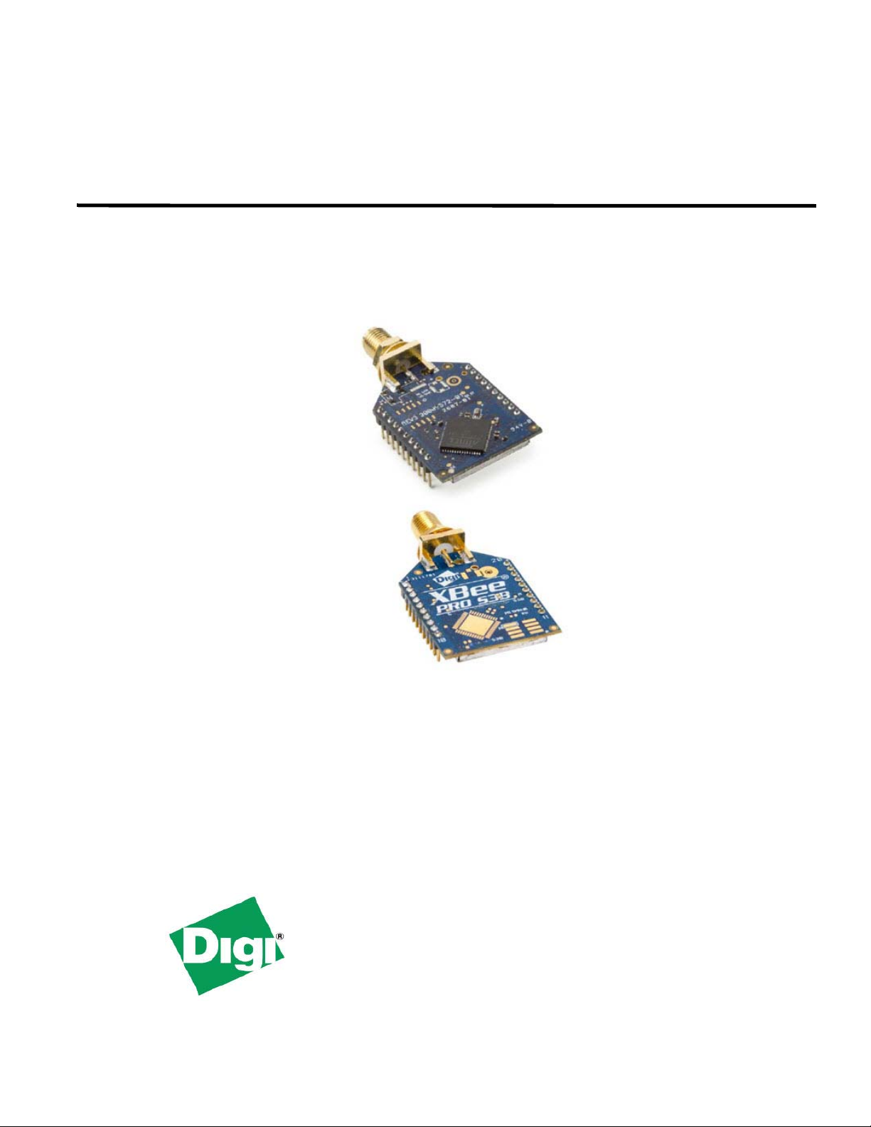
XBee-PRO® 900HP/XBee-PRO® XSC RF Modules
XBee-PRO RF Modules by Digi International
Models: XBEE-PRO S3, XBEE-PRO S3B
Hardware: S3, S3B
90002173_L
2/4/2014
Page 2

XBee‐PRO®900HP/XBee‐PRO®XSCRFModules
© 2014 Digi International Inc. All rights reserved
Nopartofthecontentsofthismanualmaybetransmittedorreproducedinany
formorbyanymeanswithoutthewrittenpermissionofDigiInternationalInc.
XBee‐PRO®isaregisteredtrademarkofDigiInternationalInc.
Technical Support: Phone: (866) 765-9885 toll-free U.S.A. & Canada
Online Support: http://www.digi.com/support
Email: rf-experts@digi.com
(801) 765-9885 Worldwide
8:00 am - 5:00 pm [U.S. Mountain Time]
©2014DigiInternationalInc. 2
Page 3

XBee‐PRO®900HP/XBee‐PRO®XSCRFModules
Contents
1. Preface: How to Use this Manual 6
2. XBee-PRO 900HP RF Module Hardware 7
XBee-PRO S3B Hardware Description 7
Worldwide Acceptance 7
XBee-PRO 900HP Specifications 8
XBee-PRO 900HP Serial Communications
Specifications 9
UART 9
SPI 9
GPIO Specifications 9
Hardware Specifications for Programmable
Variant 10
XBee-PRO 900HP Mechanical Drawings 11
XBee-PRO 900HP Pin Signals 12
XBee-PRO 900HP Design Notes 12
XBee-PRO 900HP Power Supply Design 12
XBee-PRO 900HP Recommended Pin Connections
12
XBee-PRO 900HP Board Layout 13
XBee-PRO 900HP Module Operation for
Programmable Variant 13
XBee-PRO 900HP Programmable Bootloader 15
Overview 15
Bootloader Software Specifics 15
XBee-PRO 900HP Bootloader Menu Commands 19
XBee-PRO 900HP Firmware Updates 20
Output File Configuration 20
3. XBee-PRO 900HP RF Module Operation 22
XBee-PRO 900HP Basic Operational Design 22
XBee-PRO 900HP Serial Communications 22
XBee-PRO 900HP UART Data Flow 22
XBee-PRO 900HP SPI Communications 23
XBee-PRO 900HP SPI Operation 24
XBee-PRO 900HP Configuration 25
XBee-PRO 900HP Data Format 26
XBee-PRO 900HP SPI Parameters 26
XBee-PRO 900HP Serial Buffers 27
XBee-PRO 900HP UART Flow Control 27
XBee-PRO 900HP Serial Interface Protocols 28
XBee-PRO 900HP Modes of Operation 29
XBee-PRO 900HP Description of Modes 29
Transmit Mode 29
Receive Mode 31
Command Mode 31
Sleep Mode 32
4. XBee-PRO 900HP Networking Methods 33
MAC/PHY Basics 33
Related parameters: CM, HP, ID, PL, RR, MT 33
XBee-PRO 900HP Addressing Basics 33
Related parameters: SH, SL, DH, DL, TO 33
Point to Point/Multipoint (P2MP) 34
Throughput 34
Repeater/Directed Broadcast 34
Related parameters: CE, NH, NN, BH 34
DigiMesh Networking 35
Related Command: MR 35
DigiMesh Feature Set 35
Data Transmission and Routing 35
Transmission Timeouts 36
5. XBee-PRO 900HP Sleep Mode 38
Sleep Modes 38
Normal Mode (SM=0) 38
Asynchronous Pin Sleep Mode (SM=1) 38
Asynchronous Cyclic Sleep Mode (SM=4) 38
Asynchronous Cyclic Sleep with Pin Wake Up Mode
(SM=5) 39
Synchronous Sleep Support Mode (SM=7) 39
Synchronous Cyclic Sleep Mode (SM=8) 39
Asynchronous Sleep Operation 39
Wake Timer 39
XBee-PRO 900HP Indirect Messaging and Polling
(P2MP Packets Only) 40
Indirect Messaging 40
Polling 40
Synchronous Sleep Operation (DigiMesh
networks only) 40
Operation 40
Becoming a Sleep Coordinator 43
DigiMesh Configuration 44
DigiMesh Diagnostics 46
6. XBee-PRO 900HP Command Reference Tables 47
7. XBee-PRO 900HP API Operation 58
API Frame Format 58
XBee-PRO 900HP API Serial Exchanges 60
AT Commands 60
Transmitting and Receiving RF Data 60
Remote AT Commands 60
©2014DigiInternationalInc. 3
Page 4

XBee‐PRO®900HP/XBee‐PRO®XSCRFModules
Contents
Supporting the API 61
XBee-PORO 900HP Frame Descriptions 61
AT Command 61
AT Command - Queue Parameter Value 62
TX Request 62
Explicit TX Request 63
Remote AT Command Request 65
AT Command Response 66
Modem Status 66
Transmit Status 67
Route Information Packet 67
Aggregate Addressing Update 69
RX Indicator 70
Explicit Rx Indicator 71
Data Sample RX Indicator 72
Node Identification Indicator 72
Remote Command Response 74
75
8. XBee-PRO 900HP Advanced Application Features
XBee-PRO 900HP Remote Configuration
Commands 75
Sending a Remote Command 75
Applying Changes on Remote Devices 75
Remote Command Responses 75
XBee-PRO 900HP Network Commissioning and
Diagnostics 75
XBee-PRO 900HP Device Configuration 75
XBee-PRO 900HP Network Link Establishm ent and
Maintenance 76
XBee-PRO 900HP Device Placement 76
XBee-PRO 900HP Device Discovery 77
XBee-PRO 900HP Link Reliability 78
Commissioning Pushbutton and Associate LED 81
XBee-PRO 900HP I/O Line Monitoring 82
I/O Samples 82
Queried Sampling 82
Periodic I/O Sampling 84
Digital I/O Change Detection 85
General Purpose Flash Memory 85
Accessing General Purpose Flash Memory 85
Over-the-Air Firmware Upgrades 91
Distributing the New Application 91
Verifying the New Application 92
Installing the Application 92
Things to Remember 92
Appendix A: XSC Firmware 93
XBee-PRO XSC Key Features 94
Worldwide Acceptance 94
Xbee-PRO XSC Specifications 94
XBee-PRO XSC Pin Signals 96
Xbee-PRO XSC Electrical Characteristics 97
XBee-PRO XSC Timing Specifications 97
XBee-PRO XSC Mechanical Drawings 98
Serial Communications 100
UART-Interfaced Data Flow 100
Serial Data 100
Flow Control 101
XBee-PRO XSC Modes of Operation 102
Idle Mode 102
Transmit Mode 102
Sleep Mode 104
Command Mode 106
XBee Programming Examples 109
AT Commands 109
Binary Commands 109
XBee-PRO XSC Command Reference Table 110
XBee-PRO XSC Command Descriptions 111
XBee-PRO XSC Addressing 129
Address Recognition 129
XBee-PRO XSC Basic Communications 130
Streaming Mode (Default) 130
Repeater Mode 131
XBee-PRO XSC Acknowledged Communications
135
Acknowledged Mode 135
Agency Certifications for S3B Hardware 138
FCC (United States) Certification 138
Labeling Requirements 138
FCC Notices 138
Limited Modular Approval 139
FCC-approved Antennas 139
IC (Industry Canada) Certification 139
IDA (Singapore) Certification 143
Brazil ANATEL 143
Agency Certifications for Legacy S3/S3B Hardware
144
FCC (United States) Certification 144
Labeling Requirements 144
FCC Notices 144
Limited Modular Approval 145
©2014DigiInternationalInc. 4
Page 5

XBee‐PRO®900HP/XBee‐PRO®XSCRFModules
Contents
FCC-approved Antennas 145
IC (Industry Canada) Certification 145
ANATEL (Brazil) Certification 149
Additional Information 150
©2014DigiInternationalInc. 5
Page 6

XBee‐PRO®900HP/XBee‐PRO®XSCRFModules
Preface:HowtoUsethisManual
This combined manual contains documentation for two hardware platforms: the S3 and S3B. Existing S3
customers are strongly encouraged to migrate their systems and designs to the newer and sup erior S3B
platform.
This manual also contains documentation for two RF protocols: XStream Compatible (XSC) and 900HP. The
XSC firmware is provided for customers who need compatibility with existing networks that need to be
9XStream compatible. Customers who do not require this compatibility should not use th e XSC firmware, but
rather the newer 900HP firmware.
Documentation for the XSC firmware is contained in Appendix A. All other firmware documentation in the
manual is not applicable to XSC firmware. Likewise documentation in Appendix A is not applicable to the
900HP firmware.
The following table describes how to use this manual based on the Digi part number for the module:
Digi Part
Numbers
XBP09-XC… MCQ-XBEEXSC S3 XSC XSC Appendix C
XBP9B-XC*T-001
(revision G and
earlier)
XBP9B-XC*T-002
(revision G and
earlier)
XBP9B-XC*T-021
(revision F and
earlier)
XBP9B-XC*T-022
(revision F and
earlier)
XBP9B-XC*T-001
(revision H and later)
XBP9B-XC*T-002
(revision H and later)
XBP9B-XC*T-021
(revision G and later)
XBP9B-XC*T-022
(revision G and later)
all other part numbers
beginning XBP9B-
XC...
XBP9B-D… MCQ-XB900HP S3B 900HP XSC / 900HP Appendix B
FCC ID
MCQ-XBPS3B S3B XSC XSC Appendix C
MCQ-XB900HP S3B XSC XSC / 900HP Appendix B
Hardware
Platform
Pre-installed
Firmware
Firmware
Available
Regulatory
Information
©2014DigiInternationalInc. 6
Page 7

XBee‐PRO®900HP/XBee‐PRO®XSCRFModules
1.XBee‐PRO900HPRFModuleHardware
This manual describes the operation of the XBee-PRO® 900HP RF module, which consists of firmware loaded onto XBeePRO S3B hardware.
XBee-PRO 900HP embedded RF modules provide wireless connectivity to end-point devices in mesh networks. Utilizing
the XBee-PRO Feature S et, th ese module s are inte roper a ble wi th ot her devi ces. Wi th the XBee , us ers ca n ha v e t hei r network up-and-running in a matter of minutes without configuration or additional development.
XBee-PRO S3B Hardware Description
The XBee-PRO S3B radio module hardware consists of an Energy Micro EFM32G230F128 microcontroller, an
Analog Devices ADF7023 radio transceiver, an RF power amplifier, and in the programmable version, a
Freescale MC9S08QE32 microcontroller.
Worldwide Acceptance
FCC Certified (USA) - Refer to Appendix B for FCC Requirements.
Systems that include XBee-PRO Modules in herit Digi’s FCC Certification
ISM (Industrial, Scientific & Medical) frequency band
Manufactured under ISO 9001:2000 registered standards
XBee-PRO
RoHS compliant
®
(900 MHz) RF Modules are approved for use in U.S. and Canada.
©2014DigiInternationalInc. 7
Page 8

XBee‐PRO®900HP/XBee‐PRO®XSCRFModules
XBee-PRO 900HP Specifications
SpecificationsoftheXBee-PRO® 900HP/XBee-PRO® XSCRFModule
Specification XBee
Performance
* Indoor/Urban Range
* Outdoor RF line-of-sight
Range
Transmit Power Output 24 dBm (250 mW) (software selectable)
RF Data Rate (High) 200 kbps
RF Data Rate (Low) 10 kbps
Serial UART interface CMOS Serial UART, baud rate stability of <1%
Serial Interface Data Rate
(software selectable)
Receiver Sensitivity
(typical)
Power Requirements
Supply Voltage
Transmit Current
Idle / Receive Current 29mA typical at 3.3V, (35mA max)
Sleep Current 2.5 µA (typical)
General
**Operating Frequency
Band
Dimensions
Weight 5 to 8 grams, depending on the antenna option
Operating Temperature -40º to 85º C (industrial)
Antenna Options
Digital I/O 15 I/O lines,
ADC 4 10-bit analog inputs
Networking & Security
Supported Network
Topologies
Number of Channels, user
selectable channels
Addressing Options PAN ID, Preamble ID, and 64-bit addresses
Encryption 128 bit AES
Agency Approvals
-101 dBm, high data rate, -110 dBm, low data rate
**Supply voltages of less than 3.0V may
result in reduced performance. Output
power and receiver sensitivity may be
1.297" x 0.962" x 0.215 (3.29cm x 2.44cm x 0.546cm) Note:
Dimensions do not include connector/antenna or pin lengths
Integrated wire, U. FL RF connector, Rev erse-polarity SMA
Mesh, point-to-point, point-to-multipoint, peer-to-peer
10kbps: up to 2000 ft (610m)
200kbps: up to 1000 ft (305m)
10kbps: up to 9 miles (15.5km)
200kbps: up to 4 miles (6.5km)
(with 2.1dB dipole antennas)
PL=4 : 215mA typical, (290mA max)
902 to 928 MHz (software selectable channels)
9600-230400 baud
2.1 to 3.6 VDC**
degraded.
PL=3 : 160mA typical
PL=2 : 120mA typical
PL=1 : 95mA typical
PL=0 : 60mA typical
connector
64 channels available
©2014DigiInternationalInc. 8
Page 9

XBee‐PRO®900HP/XBee‐PRO®XSCRFModules
®
SpecificationsoftheXBee-PRO
Specification XBee
United States (FCC Part
15.247)
Industry Canada (IC) 1846A-XB900HP
Australia C-Tick
Brazil ANATEL 3727-12-1209 (S3B only)
Singapore License No. DA105737 (XB900HP only)
* To determine your range, perform a range test under your operating conditions.
900HP/XBee-PRO® XSCRFModule
MCQ-XB900HP
XBee-PRO 900HP Serial Communications Specifications
XBee RF modules support both UART (Universal Asynchronous Receiver / Transmitter) and SPI (Serial
Peripheral Interface) serial connections.
UART
UARTPinAssignments
UART Pins Module Pin Number
DOUT 2
DIN / CONFIG
/ DIO7 12
CTS
/ DIO6 16
RTS
3
More information on UART operation is found in the UART section in Chapter 2.
SPI
SPIPinAssignments
For more information on SPI operation, see the SPI section in Chapter 2.
GPIO Specifications
XBee RF modules have 15 GPIO (General Purpose Input/Output) ports available. The exact list will depend on
the module configuration, as some GPIO pins are used for purposes such as serial communication.
See GPIO section for more information on configuring and using GPIO ports.
ElectricalSpecificationsforGPIOPins
GPIO Electrical Specification Value
Voltage - Supply 2.1 - 3.6 V, (3.0V or higher required for optimal performance)
Low Schmitt switching threshold 0.3 x Vdd
High Schmitt switching threshold 0.7 x Vdd
Input pull-up resistor value 40 k
Input pull-down resistor value 40 k
Output voltage for logic 0 0.05 x Vdd
Output voltage for logic 1 0.95 x Vdd
SPI Pins Module Pin Number
SPI_SCLK / DIO18 18
SPI_SSEL
SPI_MOSI / DIO16 11
SPI_MISO / DIO15 4
/ DIO17 17
SPI_ATTN
/ DIO1 19
©2014DigiInternationalInc. 9
Page 10

XBee‐PRO®900HP/XBee‐PRO®XSCRFModules
ElectricalSpecificationsforGPIOPins
GPIO Electrical Specification Value
Output source current 2 mA
Output sink current 2 mA
Total output current (for GPIO pins) 48 mA
Hardware Specifications for Programmable Variant
If the module has the programmable secondary processor, add the following table values to the specifications
listed on page 7. For example, if the secondary processor is running at 20 MHz and the primary processor is in
receive mode then the new current value will be I
runtime current of the secondary processor and I
Specificationsoftheprogrammablesecondaryprocessor
Optional Secondary Processor Specification
Runtime current for 32k running at 20MHz +14mA
Runtime current for 32k running at 1MHz +1mA
Sleep current +0.5A typical
For additional specifications see Freescale Datasheet and
Manual
Voltage requirement for secondary processor to operate at
maximum clock frequency
Minimum Reset Pulse for Programmable 100nS
Minimum Reset Pulse to Radio 50nS
VREF Range 1.8VDC to VCC
= Ir2 + I
total
is the receive current of the primary.
rx
= 14 mA + 9 mA = 23 mA, where I
rx
(Add to RX, TX, and sleep currents depending on
These numbers add to specifications
mode of operation)
MC9SO8QE32
2.4 to 3.6VDC
r2
is the
©2014DigiInternationalInc. 10
Page 11
XBee‐PRO®900HP/XBee‐PRO®XSCRFModules
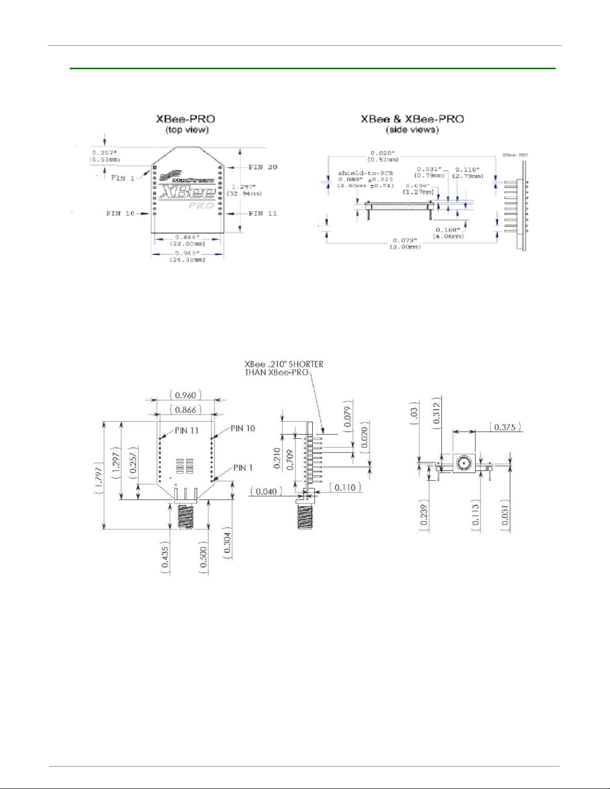
XBee-PRO 900HP Mechanical Drawings
MechanicaldrawingsoftheXBee‐PRO900HPRFModules(antennaoptionsnotshown).Alldimensionsareininches.
.
©2014DigiInternationalInc. 11
Page 12

XBee‐PRO®900HP/XBee‐PRO®XSCRFModules
XBee-PRO 900HP Pin Signals
PinAssignmentsforXBeeModules
Pin # Name Direction Default State Description
1 VCC Power Supply
2 DOUT/DIO13 Both Output GPIO / UART Data out
3 DIN/nConfig/DIO14 Both Input GPIO / UART Data In
4 DIO12/SPI_MISO Both Output GPIO / SPI slave out
5 nRESET I nput
6 DIO10/PWM0
7 DIO11/PWM1 Both GPIO / Pulse Width Modulator
8 reserved Disabled Do Not Connect
9 nDTR/SLEEP_RQ/DIO8 Both Input
10 GND Ground
11 DIO4/AD4/SPI_MOSI Both GPIO/SPI slave In
12 nCTS/DIO7 Both Output GPIO / Clear-to-Send Flow Control
13 On_nSLEEP/DIO9 Output Output GPIO / Module Status Indicator
14 VREF Input
15 Associate/DIO5 Both Output GPIO / Associate Indicator
16 nRTS/DIO6 Both Input GPIO / Request-to-Send Flow Control
17 AD3/DIO3/SPI_nSSEL Both GPIO / Analog Input / SPI Slave Select
18 AD2/DIO2/SPI_CLK Both GPIO / Analog Input / SPI Clock
19 AD1/DIO1/SPI_nATTN Both GPIO / Analog Input / SPI Attention
20 AD0/DIO0 Both GPIO / Analog Input
(Low‐assertedsignalsaredistinguishedwithahorizontallineabovesignalname.)
Module Reset. Drive low to reset the modu le. This
is also an output with an open drain configuration
with an internal 20 K ohm pull-up (never drive to
logic high, as the module may be driving it low).
The minimum pulse width is 1 mS.
Both GPIO / RX Signal Strength Indicator
GPIO / Pin Sleep Control Line (DTR on the dev
board)
Internally used for programmable secondary
processor. For compatibility with other XBee
modules, we recommend connecting this pin to the
voltage reference if Analog Sampling is desired.
Otherwise, connect to GND.
• Signal Direction is specified with respect to the module
• See Design Notes section below for details on pin connections.
XBee-PRO 900HP Design Notes
The XBee modules do not specifically require any external circuitry or specific connections for proper
operation. However, t here are some general design guidelines that are recommended for help in
troubleshooting and building a robust design.
XBee-PRO 900HP Power Supply Design
Poor power supply can lead to poor radio performance, especially if the supply voltage is not kept within
tolerance or is excessively noisy. To help reduce noise, we recommend placing both a 1F and 47pF capacitor
as near to pin 1 on the PCB as possible. If using a switching regulator for your power supply, switching
frequencies above 500kHz are preferred. Power supply ripple should be limited to a maximum 50mV peak to
peak.
Note – For designs using the programmable modules, an additional 10F decoupling cap is recommended near
pin 1 of the module. The nearest proximity to pin 1 of the three caps should be in the following order: 47pf,
1F followed by 10F.
XBee-PRO 900HP Recommended Pin Connections
The only required pin connections are VCC, GND, DOUT and DIN. To support serial firmware updates, VCC,
GND, DOUT, DIN, RTS, and DTR should be connected.
©2014DigiInternationalInc. 12
Page 13

XBee‐PRO®900HP/XBee‐PRO®XSCRFModules
All unused pins should be left disconnected. All inputs on the radio can be pulled high or low with 40k internal
pull-up or pull-down resistors using the PR and PD software commands. No specific treatment is needed for
unused outputs.
For applications that need to ensure the lowest sleep current, unconnected inputs should never be left
floating. Use internal or external pull-up or pull-down resistors, or set the unused I/O lines to outputs.
Other pins may be connected to external circuitry for convenience of operation, including the Associate LED
pin (pin 15) and the Commissioning pin (pin 20). An LED attached to the the associate LED pin will flash
differently depending on the state of the module to the network, and a pushbutton attached to pin 20 can
enable various join functions without having to send serial p ort commands. Please see the commissioning
pushbutton and associate LED section in chapter 7 for more details. The source and sink capabilities are
limited to 6mA on all I/O pins.
The VRef pin (pin 14) is only used on the programmable versions of these modules. For compatibility with
other XBee modules, we recommend connecting this pin to a voltage reference if analog sampling is desired.
Otherwise, connect to GND.
XBee-PRO 900HP Board Layout
XBee modules are designed to be self sufficient and have minimal sensitivity to nearby processors, cr ystals or
other PCB components. As with all PCB designs, Power and Ground traces should be thicker than signal traces
and able to comfortably support the maximum current specifications. No other special PCB design
considerations are required for integrating XBee radios except in the antenna section.
The choice of antenna and antenna location is very important for correct performance. XBees do not require
additional ground planes on the host PCB. In general , antenna elem ents r adiate perpendicular to the dire ction
they point. Thus a vertical antenna emits across the horizon. Metal objects near the antenna cause reflections
and may reduce the ability for an antenna to radiate efficiently. Metal objects between the transmitter and
receiver can also block the radiation path or reduce the transmission distance, so external antennas should be
positioned away from them as much as possible. Some objects that are often overlooked are metal poles,
metal studs or beams in structures, concrete (it is usually reinforced with metal rods), metal enclosures,
vehicles, elevators, ventilation ducts, refrigerators, microwave ovens, batteries, and t all electrolytic
capacitors.
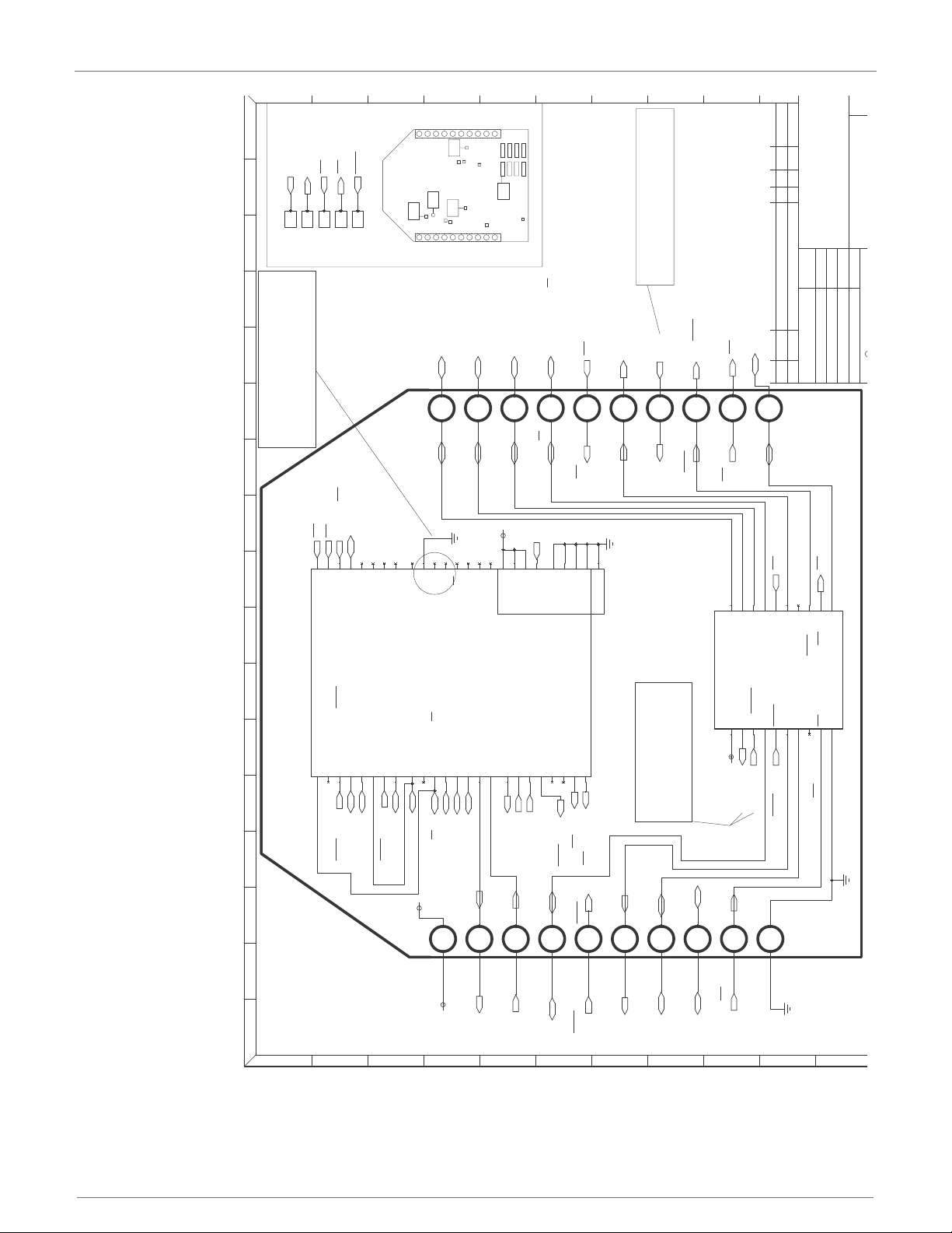
XBee-PRO 900HP Module Operation for Programmable Variant
The modules with the programmable opti on have a s econdary processor with 32k of flash and 2k of RAM. This
allows module integrators to put custom code on the XBee module to fit their own unique needs. The DIN,
DOUT, RTS, CTS, and RESET lines are intercepted by the secondary processor to allow it to be in control of the
data transmitted and received. All other lines are in parallel and can be controlled by either the internal
microcontroller or the MC9SO8QE micro (see Block Diagram for details). The internal microcontroller by
default has control of certain lines. These lines can be released by the internal microcontroller by sending the
proper command(s) to disable the desired DIO line(s) (see XBee Command Reference Tables).
In order for the secondary processor to sample with ADCs, the XBee pin 14 (VREF) must be connected to a
reference voltage.
Digi provides a bootloader that can take care of programming the processor over the air or through the serial
interface. This means that over the air updates can be supported through an XMODEM protocol. The processor
can also be programmed and debugged through a one wire interface BKGD (Pin 8).
©2014DigiInternationalInc. 13
Page 14
XBee‐PRO®900HP/XBee‐PRO®XSCRFModules
GND
A
5
4
G
E
12
9
ECO
PART NO.
B
14
2
13
11
REV
TITLE
DATE:
1
ENGINEER:
APPROVALS:
REV
DATE
10
17
16
15
8
3
F
APPR
CKD
BY
C
D
6
DESCRIPTION OF CHANGE
E
G
F
7
DESIGNED:
CHECKED:
DRAWN:
D
C
B
A
L
K
J
H
J
H
Digi Internat ional I nc
C
DOUT/PTB1
DIO3/ADC3/PTB5,A7/SS
BKGD/PTA4
DIO0/ADC0/PTA0
ON/SLEEP/PTA1
CTS/DIO7/PTC0
DIO4/PTB3/MOSI1
BKGD/PTA4
DIO12/PTB4/MISO1
DIN_RADIO
DOUT_RADIO
ASSOC/DIO5/PTD4
RTS/DIO6/PTD7
CTS_RADIO
VREF
CTS_RADIO
SLEEP_RQ/DTR/PTD5
RESET/PTA5
DIO1/ADC1/PTA3/SCL
RESET/PTA5
ASSOC/DIO5/PTD4
DIO2/ADC2/PTB2/SPSCK
DOUT_RADIO
DIN_RADIO
RESET_RADIO
ASSOC/DIO5/PTD4
ON/SLEEP/PTA1
ON/SLEEP/PTA1
RSSI/DIO10/PWM0/PTC 5
DIO1/ADC1/PTA3/SCL
VREF
RTS/DIO6/PTD7
DIO2/ADC2/PTB2/SPSCK
DIO3/ADC3/PTB5,A7/SS
RTS/DIO6/PTD7
DIO2/ADC2/PTB2/SPSC K
DIN/PTB0
VREF
DIO11/PWM1/PTA2/SDA
RTS_RADIO
DIO1/ADC1/PTA3/SCL
DIO12/PTB4/MISO1
DIN/PTB0
SLEEP_RQ/DTR/PTD5
DIO4/PTB3/MOSI1
BKGD/PTA4
DIN_RADIO
DIO12/PTB4/MISO1
DOUT_RADIO
CTS/DIO7/PTC0
DIO11/PWM1/PTA2/SDA
DIO0/ADC0/PTA0
RTS_RADIO
RTS_RADIO
DIO4/PTB3/MOSI1
DOUT/PTB1
CTS/DIO7/PTC0
DIO0/ADC0/PTA0
CTS_RADIO
RESET_RADIO
DIO3/ADC3/PTB5,A7/SS
RSSI/DIO10/PWM0/PTC 5
SLEEP_RQ/DTR/PTD5
RESET/PTA5
RSSI/DIO10/PWM0/PTC5
DIO11/PWM1/PTA2/SDA
RESET_RADIO
VCC
VCC
VCC
VCC
123456789
10
111213141516171819
20
VCC
GND
RESERVED
DIN/CONFIG
DOUT
DTR/SLEEP_RQ/DIO8
PWM0/RSSI/DIO10
PWM1/DIO11
RESET
PWM2/DIO12
CTS/DIO7
RTS/AD6/DIO6
VREF
AD1/DIO1
AD2/DIO2
DIO4
AD3/DIO3
AD0/DIO0
ASSOC/AD5/DIO5
ON/SLEEP/DIO9
S
2728474835363738101114152324252639404546161721
22
44434241291312
321343332201918
PTB6/SDA/XTAL
PTB1/KBI1P15/TxD1/ADP5
PTB2/KBIP6/SPSCK/ADP6
PTB3/KBIP7/MOSI/ADP7
PTB4/TPM2CH1/MISO
PTB5/TPM1CH1/SS
PTE6
PTD6/KBI2P6
PTA3/KBIP3/SCL/ADP3
PTA0/KBI1P0/TPM1CH0/ADP0/ACMP1+
PTA4/ACPM1O/BKGD/MS
PTA7/TPM2CH2/ADP9
PTA1/KBI1P1/TPM2CH0/ADP1/ACMP1-
PTA5/IRQ/TPM1CLK/RESET
PTA6/TPM1CH2/ADP8
PTA2/KBI1P2/SDA/ADP2
PTE4
PTE5
PTE3/SS
PTE2/MISO
PTD7/KBI2P7
PTD1/KBI2P1
PTD2/KBI2P2
PTD3/KBI2P3
PTD5/KBI2P5
PTE0/TPM2CLK/SPSCLK
PTD4/KBI2P4
PTB7/SCL/EXTEL
PTE1/MOSI
PTD0/KBI2P0
PTC4/TPM3CH4
PTB0/KBI1P4/RxD1/ADP4
PTC2/TPM3CH2
PTC7/TxD2/ACPM2-
PTC5/TPM3CH5/ACPM2O
PTC3/TPM3CH3
PTC1/TPM3CH1
PTC0/TPM3CH0
PTE7/TPM3CLK
PTC6/RxD2/ACPM2+
U1-A
MC9S08QE32CFT
304567893149
VSS
VSSAD
VREFL
VSS
VDD
VDD
VDDAD
PAD
VREFH
U1-B
MC9S08QE32CFT
14
8
Commissioning Line
19
10
20
1
9
6
354
2
FREESCALE
A
11
TP5
7
13
TP2
Pin10
Pin11
TP1
VREF must be connected to
external reference for MC9S08
to sample ADC lines
Special Test Points
TP6
XBEE-PRO S3B
PROGRAMMABLE
BLOCK DIAGRAM
TP4
15
Pin1
Pin20
Commissioning Line
MC9S08 controls
DOUT, DIN, RESET, RTS, CTS
for Internal Radio.
These lines are not
connected to the
20 external pins.
TP1
12
Pins PTE4, 5 and 6 are used so
software can determ
ine
fundamental Hardware differences
by turning on internal pull-up
resistors and reading the lines.
011 = Programmable S3B
PROGRAMMABLE XBEE-PRO S3B
16
TP2
18
TP5
TP4
17
TP6
S3B RADIO
©2014DigiInternationalInc. 14
Page 15

XBee‐PRO®900HP/XBee‐PRO®XSCRFModules
XBee-PRO 900HP Programmable Bootloader
Overview
The XBee Programmable module is equipped with a Freescale MC9S08QE32 application processor. This
application processor comes with a supplied bootloader. This section describes how to interface the customer's
application code running on this processor to the XBee Programmable module's supplied bootloader.
The first section discusses how to initiate firmware updates using the supplied bootloader for wired and overthe-air updates.
Bootloader Software Specifics
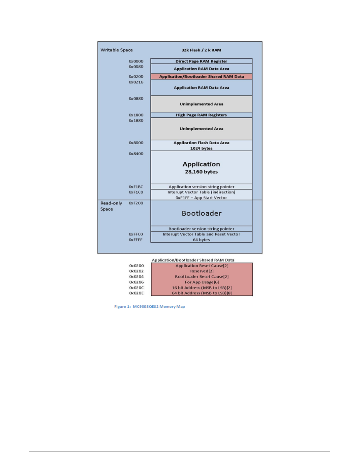
Memory Layout
Figure 1 shows the memory map for the MC9S08QE32 application processor.
The supplied bootloader occupies the bottom pages of the flash from 0xF200 to 0xFFFF. Application
code cannot write to this space.
The application code can exist in Flash from address 0x8400 to 0xF1BC. 1k of Flash from 0x8000 to
0x83FF is reserved for Non Volatile Application Data that will not be erased by the bootloader during a
flash update.
A portion of RAM is accessible by both the application and the bootloader. Specifically, there is a shared
data region used by both the application and the bootloader that is located at RAM address 0x200 to
0x215. Application code should not write anything to BLResetCause or AppResetCause unless
informing the bootloader of the impending reset reason. The Application code should not clear
BLResetCause unless it is handling the unexpected reset reason.
T o prevent a malfunctioning application from running forever, the Bootloader increments BLResetCause
after each watchdog or illegal instruction reset. If this register reaches above 0x10 the bootloader will
stop running the application for a few minutes to allow an OTA or Local update to occur. If no update is
initiated within the time period, BLResetCause is cl ear ed and the application is started again. To
prevent unexpected halting of the application, the application shall clear or decrement BLResetCause
just before a pending reset. To disable this feature, the application shall clear BLResetCause at the
start of the application.
©2014DigiInternationalInc. 15
Page 16
XBee‐PRO®900HP/XBee‐PRO®XSCRFModules
©2014DigiInternationalInc. 16
Page 17

XBee‐PRO®900HP/XBee‐PRO®XSCRFModules
Operation
Upon reset of any kind, the execution control begins with the bootloader.
If the reset cause is Power-On reset (POR), Pin reset (PIN), or Low Voltage Detect (LVD) reset (LVD)
the bootloader will not jump to the application code if the override bits are set to RTS(D7)=1,
DTR(D5)=0, and DIN(B0)=0. Otherwise, the bootloader writes the reset cause "NOTHING" to the
shared data region, and jumps to the Application.
Reset causes are defined in the file common. h in an enumeration with the following definitions:
typedef enum {
BL_CAUSE_NOTHING = 0x0000, //PIN, LVD, POR
BL_CAUSE_NOTHING_COUNT = 0x0001,//BL_Reset_Cause counter
// Bootloader increments cause every reset
BL_CAUSE_BAD_APP = 0x0010,//Bootloader considers APP invalid
} BL_RESET_CAUSES;
typedef enum {
APP_CAUSE_NOTHING = 0x0000,
APP_CAUSE_USE001 = 0x0001,
// 0x0000 to 0x00FF are considered valid for APP use.
APP_CAUSE_USE255 = 0x00FF,
APP_CAUSE_FIRMWARE_UPDATE = 0x5981,
APP_CAUSE_BYPASS_MODE = 0x4682,
APP_CAUSE_BOOTLOADER_MENU = 0x6A18,
} APP_RESET_CAUSES;
Otherwise, if the reset cause is a "watchdog" or other reset, the bootloader checks the shared memory
region for the APP_RESET_CAUSE. If the reset cause is:
1."APP_CAUSE_NOTHING" or 0x0000 to 0x00FF, the bootloader increments the
BL_RESET_CAUSES, verifies that it is still less than BL_CAUSE_BAD_APP , and jumps back to
the application. If the Application does not clear the BL_RESET_CAUSE, it can prevent an
infinite loop of running a bad application that continues to perform illegal instructions or
watchdog resets.
2."APP_CAUSE_FIRMWARE_UPDATE", the bootloader has been instructed to update the
application "over-the-air" from a specific 64-bit address. In this case, the bootloader will
attempt to initiate an Xmodem transfer from the 64-bit address located in shared RAM.
3."APP_CAUSE_BYPASS_MODE", the bootloader executes bypass mode. This mode passes the
local UART data direc tly to the internal mi crocontroller allowing for dire ct communicati on with
the internal microcontroller.
The only way to exit bypass mode is to reset or power cycle the module.
If none of the above is true, the bootloader will enter "Command mode". In this mode, users can
initiate firmware downloads both wired and over-the-air, check application/bootloader version strings,
and enter Bypass mode.
Application version string
Figure 1 shows an "Application version string pointer" area in application flash which holds the pointer
to where the application version string resides. The application's linker command file ultimately
determines where this string is placed in application flash.
It is preferable that the application version string be loca ted at address 0x8400 for MC9S08QE32 parts .
The application string can be any characters terminated by the NULL character (0x00). There is not a
strict limit on the number of characters in the string, but for practical purposes should be kept under
100 bytes including the terminating NULL character. During an update the bootloader erases the entire
application from 0x8400 on. The last page has the vector table specifically the redirected reset vec to r.
The version string pointer and reset vector are used to determine if the application is valid.
©2014DigiInternationalInc. 17
Page 18

XBee‐PRO®900HP/XBee‐PRO®XSCRFModules
Application Interrupt Vector table and Linker Command File
Since the bootloader flash region is read-only, the interrupt vector table is redirected to the region
0xF1C0 to 0xF1FD so that application developers can use hardware interrupts. Note that in order for
Application interrupts to function properly, the Application's linker command file (*.prm extension)
must be modified appropriately to allow the linker to place the developers code in the correct place in
memory. For example, the developer desires to use the serial communications port SCI1 receive
interrupt. The developer would add the following line to the Codewarrior linker command file for the
project:
VECTOR ADDRESS 0x0000F1E0 vSci1Rx
This will inform the linker that the interrupt function "vSci1Rx()" should be placed at address
0x0000F1E0. Next, the developer should add a file to their project "vector_table.c" that creates an
array of function pointers to the ISR routines used by the application.
extern void _Startup(void);/* _Startup located in Start08.c */
extern void vSci1Rx(void);/* sci1 rx isr */
extern short iWriteToSci1(unsigned char *);
void vDummyIsr(void);
#pragma CONST_SEG VECTORS
void (* const vector_table[])(void) = /* Relocated Interrupt vector table */{
vDummyIsr,/* Int.no. 0 Vtpm3ovf (at F1C0)Unassigned */
vDummyIsr, /* Int.no. 1 Vtpm3ch5 (at F1C2) Unassigned */
vDummyIsr, /* Int.no. 2 Vtpm3ch4 (at F1C4) Unassigned */
vDummyIsr, /* Int.no. 3 Vtpm3ch3 (at F1C6) Unassigned */
vDummyIsr, /* Int.no. 4 Vtpm3ch2 (at F1C8) Unassigned */
vDummyIsr, /* Int.no. 5 Vtpm3ch1 (at F1CA) Unassigned */
vDummyIsr, /* Int.no. 6 Vtpm3ch0 (at F1CC) Unassigned */
vDummyIsr, /* Int.no. 7 Vrtc (at F1CE) Unassigned */
vDummyIsr, /* Int.no. 8 Vsci2tx (at F1D0) Unassigned */
vDummyIsr, /* Int.no. 9 Vsci2rx (at F1D2) Unassigned */
vDummyIsr, /* Int.no. 10 Vsci2err (at F1D4) Unassigned */
vDummyIsr, /* Int.no. 11 Vacmpx (at F1D6) Unassigned */
vDummyIsr, /* Int.no. 12 Vadc (at F1D8) Unassigned */
vDummyIsr, /* Int.no. 13 Vkeyboard (at F1DA) Unassigned */
vDummyIsr, /* Int.no. 14 Viic (at F1DC) Unassigned */
vDummyIsr, /* Int.no. 15 Vsci1tx (at F1DE) Unassigned */
vSci1Rx, /* Int.no. 16 Vsci1rx (at F1E0) SCI1RX */
vDummyIsr, /* Int.no. 17 Vsci1err (at F1E2) Unassigned */
vDummyIsr, /* Int.no. 18 Vspi (at F1E4) Unassigned */
vDummyIsr, /* Int.no. 19 VReserved12 (at F1E6) Unassigned */
vDummyIsr, /* Int.no. 20 Vtpm2ovf (at F1E8) Unassigned */
vDummyIsr, /* Int.no. 21 Vtpm2ch2 (at F1EA) Unassigned */
vDummyIsr, /* Int.no. 22 Vtpm2ch1 (at F1EC) Unassigned */
vDummyIsr, /* Int.no. 23 Vtpm2ch0 (at F1EE) Unassigned */
vDummyIsr, /* Int.no. 24 Vtpm1ovf (at F1F0) Unassigned */
vDummyIsr, /* Int.no. 25 Vtpm1ch2 (at F1F2) Unassigned */
vDummyIsr, /* Int.no. 26 Vtpm1ch1 (at F1F4) Unassigned */
vDummyIsr, /* Int.no. 27 Vtpm1ch0 (at F1F6) Unassigned */
©2014DigiInternationalInc. 18
Page 19

XBee‐PRO®900HP/XBee‐PRO®XSCRFModules
vDummyIsr, /* Int.no. 28 Vlvd (at F1F8) Unassigned */
vDummyIsr, /* Int.no. 29 Virq (at F1FA) Unassigned */
vDummyIsr, /* Int.no. 30 Vswi (at F1FC) Unassigned */
_Startup /* Int.no. 31 Vreset (at F1FE) Reset vector */
};
void vDummyIsr(void){
for(;;){
if(iWriteToSci1("STUCK IN UNASSIGNED ISR\n\r>"));
}
}
The interrupt routines themselves can be defined in separate files. The "vDummyIsr" function is used
in conjunction with "iWritetoSci1" for debugging purposes.
XBee-PRO 900HP Bootloader Menu Commands
The bootloader accepts commands from both the local UART and OTA. All OTA commands sent must be
Unicast with only 1 byte in the payload for each command. A response will be returned to the sender. All
Broadcast and multiple byte OTA packets are dropped to help prevent general OTA traffic from being
interpreted as a command to the bootloader while in the menu.
Bypass Mode - "B"
The bootloader provides a “bypass” mode of operation that essentially connects the freescale mcu to
the internal microcontroller’s serial UART. This allows direct communication t o the internal
microcontroller’s radio for the purpose of firmware and radio configuration changes. Once in bypass
mode, the X-CTU utility can change modem configuration and/or update module’s firmware. Bypass
mode automatically handles any baud rate up to 115.2kbps. Note that this command is unavailable
when module is accessed remotely.
Update Firmware - "F"
The "F" command initiates a firmware download for both wired and over-the-air configurations.
Depending on the source of the command (received via Over the Air or local UART), the download will
proceed via wired or over-the-air respectively.
Adjust Timeout for Update Firmware - "T"
The "T" command changes the timeout before sending a NAK by Base-Time*2^(T). The Base- Time for
the local UART is different than the Base-Time for Over the Air. During a firmware update, the
bootloader will automatically increase the Timeout if repeat packets are received or multiple NAKs for
the same packet without success occur.
Application Version String - "A"
The "A" command provides the version of the currently loaded application. If no application is present,
"Unkown" will be returned.
Bootloader Version String - "V"
The "V" command provides the version of the currently loaded bootloader. The version will return a
string in the format BLFFF-HHH-XYZ_DDD where FFF repr esents the Flash size in kilo bytes, HHH is the
hardware, XYZ is the version, and DDD is the preferred XMODEM packet size for updates. Double the
preferred packet size is also possible, but not guaranteed. For example "BL032-2 B0-023_064" will ta ke
64 byte CRC XMODEM payloads and may take 128 byte CRC XMODEM payloads also. In this case, both
64 and 128 payloads are handled, but the 64 byte payload is preferred for better Over the Air
reliability.
Bootloader Version BL032-2x0-025_064 only operates at 9600 baud on the local UART as well as
communications to the internal microc ontroller. A newer version of the Bootloader BL032-2x0-033_064
or newer BL032-2B0-XXX_064 has changed the baud rate to 115200 between the Programmable and
©2014DigiInternationalInc. 19
Page 20

XBee‐PRO®900HP/XBee‐PRO®XSCRFModules
the internal microcontroller. The internal module is also set to 115200 as the default baud rate. The
default rate of the programmable local UART is also set to 115200, however, the local UART has an
auto baud feature added to detect if the UART is at the wrong baud rate. If a single character is sent, it
will automatically switch to 115200 or 9600 baud.
XBee-PRO 900HP Firmware Updates
Wired Updates
A user can update their application using the bootloader in a wired configuration with the following
steps:
a. Plug XBee programmable module into a suitable serial port on a PC.
b. Open a hyperterminal (or similar dumb terminal application) session with 115200 baud, no par-
ity, and 8 data bits with one stop bit.
c. Hit Enter to display the bootloader menu.
d. Hit the "F" key to initiate a wired firmware update.
e. A series of "C" characters Will be displayed within the hyperterminal window. At this point,
select the "transfer->send file" menu item. Select the desired flat binary output file.
f. Select "Xmodem" as the protocol.
g. Click "Send" on the "Send File" dialog. The file will be downloaded to the XBee Programmable
module. Upon a successful update, the bootloader will jump to the newly loaded application.
Over-The-Air updates
A user can update their application using the bootloader in an “over-the-air” configuration with the
following steps…(This procedure assumes that the bootloader is running and not the application. The
internal microcontroller baud rate of the programmable module must be set to 115200 baud. The
bootloader only operates at 115200 baud between the Radio and programmable bootloader. The
application must be programmed with some way to support returning to the bootloader in order to
support Over the Air (OTA) updates without local intervention.)
a. Open a hyperterminal session to the host module with no parity, no hardwareflow control, 8
data bits and 1 stop bit. (The host module does not have to operate at the same baud rate as the
remote module.) For faster updates and less latency due to the UART, set the host module to a
faster baud rate. (i.e. 115200)
b. Enter 3 pluses "+++" to place the module in command mode. (or XCTU’s “Modem Configuration” tab can be used to set the correct parameters)
c. Set the Host Module destination address to the target module’s 64 bit address that the host
module will update (ATDH aabbccdd, ATDL eeffgghh, ATCN, where aabbccddeeffgghh is the hexadecimal 64 bit address of the target module).
d. Hit Enter and the bootloader command menu will be displayed from the remote module. (Note
that the option "B" doesn't exist for OTA)
e. Hit the "F" key to cause the remote module to request the new firmware file over-the-air.
f. The host module will begin receiving "C" characters indicating that the remote module is
requesting an Xmodem CRC transfer. Using XCTU or another terminal program, Select "XMODEM"
file transfer. Select the Binary file to upload/transfer. Click Send to start the transfer. At the conclusion of a successful transfer, the bootloader will jump to the newly loaded application.
Output File Configuration
BKGD Programming
P&E Micro provides a background debug tool that allows flashing applications on the MC9S08QE parts
through their background debug mode port. By default, the Codewarrior tool produces an "ABS" output
file for use in programming parts through the background debug interface. The programmable XBee
from the factory has the BKGD debugging capability disabled. In order to debug, a bootloader with the
©2014DigiInternationalInc. 20
Page 21

XBee‐PRO®900HP/XBee‐PRO®XSCRFModules
debug interface enabled needs to be loaded on the secondary processor or a stand-alone app needs to
be loaded.
Bootloader updates
The supplied bootloader requires files in a "flat binary" format which differs from the default ABS file
produced. The Codewarrior tool also produces a S19 output file. In order to successfully flash new
applications, the S19 file must be converted into the flat binary format. Utilities are available on the
web that will convert S19 output to "BIN" outputs. Often times, the "BIN" file conversion will pad the
addresses from 0x0000 to the code space with the same number. (Often 0x00 or 0xFF) These extra
bytes before the APP code starts will need to be deleted from the bin file before the file can be
transferred to the bootloader.
©2014DigiInternationalInc. 21
Page 22
XBee‐PRO®900HP/XBee‐PRO®XSCRFModules
Packet Handler
Transparent
Mode
AT Command
Mode
API
Mode
Network Layer (DigiMesh/Repeater)
MAC/PHY Layer (Point-Multipoint)
UART SPI
2.XBee‐PRO900HPRFModuleOperation
XBee-PRO 900HP Basic Operational Design
The XBee-PRO® 900HP RF Module uses a multi-layered firmware base to order the flow of data, dependent on the
hardware and software configuration chosen by the user. This configuration block diagram is shown below, with the
host serial interface as the physical starting point, and the antenna as the physical endpoint for the transferred data.
As long as a block is able to touch another block, the two interfaces can interact. For example, if the module is using
SPI mode, Transparent Mode is not available. See below:
Host Serial Interface
Command Handler
Antenna
The command handler is the code that processes commands from AT Command Mode or API Mode (see AT Commands section). The command handler can also proces s commands from re mote r adios ( see Remote AT Command s
section).
XBee-PRO 900HP Serial Communications
XBee RF Modules interface to a host device through a serial port. Through its serial port, the module can
communicate with any logic and voltage compatible UART, through a level translator to any serial device (for
example, through a RS-232 or USB interface board), or through a Serial Peripheral Interface (SPI), which is a
synchronous interface to be described later.
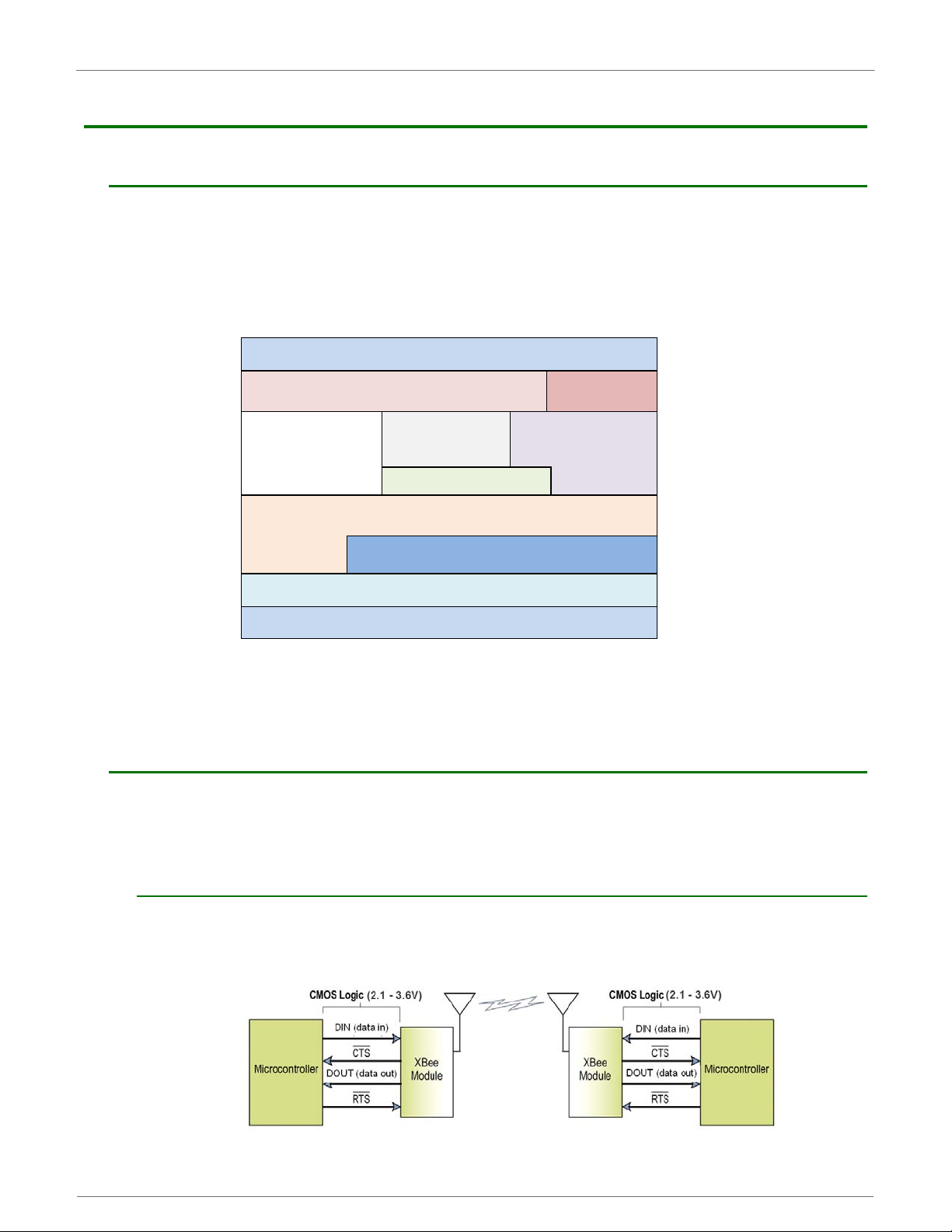
XBee-PRO 900HP UART Data Flow
Devices that have a UART interface can connect directly to the pins of the RF module as shown in the figure
below.
SystemDataFlowDiagraminaUART‐interfacedenvironment
(Low‐assertedsignalsdistinguishedwithhorizontallineoversignalname.)
©2014DigiInternationalInc. 22
Page 23
XBee‐PRO®900HP/XBee‐PRO®XSCRFModules
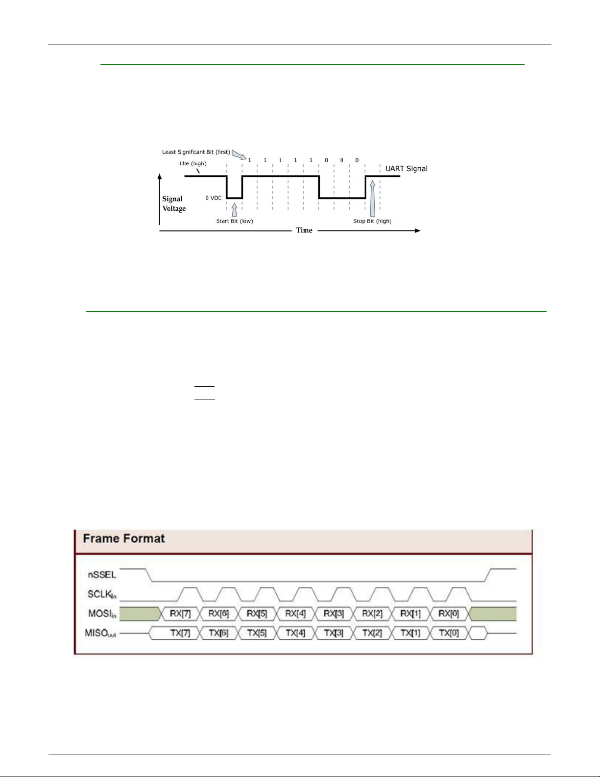
Serial Data
Data enters the module UART through the DIN (pin 3) as an asynchronous serial signal. The signal should
idle high when no data is being transmitted.
Each data byte consists of a start bit (low), 8 data bits (least signif ic ant bit first) and a stop bit (high). The
following figure illustrates the serial bit pattern of data passing through the module.
UARTdatapacket0x1F(decimalnumberʺ31ʺ)astransmittedthroughtheRFmodule
ExampleDataFormatis8‐N‐1(bits‐parity‐#ofstopbits)
Serial communications depend on the two UARTs (the microcontroller's and the RF module's) to be
configured with compatible settings (baud rate, parity, start bits, stop bits, data bits).
The UART baud rate, parity, and stop bits settings on the XBee module can be configured with the BD, NB,
and SB commands respectively. See the command table in chapter 10 for details.
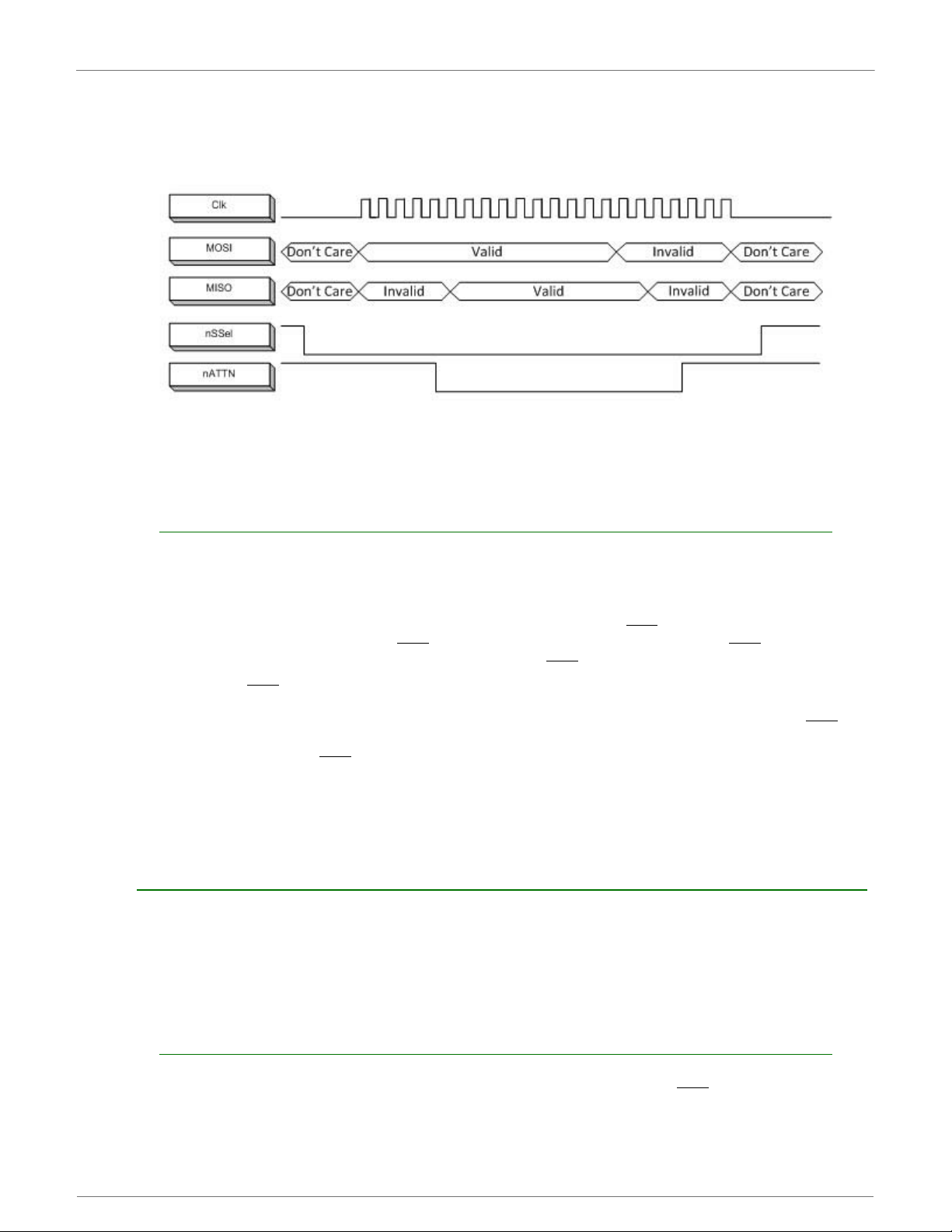
XBee-PRO 900HP SPI Communications
The XBee modules support SPI communications in slave mode. Sla ve mode receiv es the clock signal and data
from the master and returns data to the master. The SPI port uses the following signals on the XBee:
• SPI_MOSI (Master Out, Slave In) - inputs serial data from the master
• SPI_MISO (Master In, Slave Out) - outputs serial data to the master
• SPI_SCLK (Serial Clock) - clocks data transfers on MOSI and MISO
•SPI_SSEL
•SPI_ATTN
ule will assert this pin as soon as data is available to send to the SPI master and it will remain
asserted until the SPI master has clocked out all available data.
In this mode, the following apply:
• SPI Clock rates up to 3.5 MHz are possible.
• Data is MSB first
• Frame Format mode 0 is used. This means CPOL=0 (idle clock is low) and CPHA=0 (data is
sampled on the clock’s leading edge). Mode 0 is diagramed below.
• SPI port is setup for API mode and is equivalent to AP=1.
(Slave Select) - enables serial communication with the slave
(Attention) - alerts the master that slave has data que ued to send. The XBee mod-
FrameFormatforSPICommunications
©2014DigiInternationalInc. 23
Page 24

XBee‐PRO®900HP/XBee‐PRO®XSCRFModules
XBee-PRO 900HP SPI Operation
This section specifies how SPI is implemented on the XBee, what the SPI signals are, and how full duplex
operations work.
XBee Implementation of SPI
The module operates as a SPI slave only. This means that an external master will provide the clock and will
decide when to send. The XBee-PRO 900HP supports an external clock rate of up to 3.5 Mbps.
Data is transmitted and received with most significant bit first using SPI mode 0. This means the CPOL and
CPHA are both 0. Mode 0 was chosen because it's the typical default for most microcontrollers and would
simplify configuration of the master. Further information on Mode 0 is not included in this manual, but is welldocumented on the internet.
XBee-PRO 900HP SPI Signals
The official specification for SPI includes the four sign als SPI_MISO, SPI_MOSI, SPI_CLK, and SPI_SSEL.
Using only these four signals, the master cannot know when the sl ave needs to se nd and the SPI slav e cannot
transmit unless enabled by the master. For this reason, the SPI_ATTN
allows the module to alert the SPI master that it has data to send. In turn, the SPI master is expected to
assert SPI_SSEL
in turn, allows the XBee module to send data to the master.
The table below names the SPI signals and specifies their pinouts. It also describes the operation of each pin:
and start SPI_CLK, unless these signals are already asserted and active respectively. This,
signal is available in the design. This
Signal Name Pin Number
SPI_MISO
(Master In, Slave out)
SPI_MOSI
(Master out, Slave in)
SPI_SSEL
(Slave Select)
(Master out, Slave in)
SPI_CLK
(Clock)
(Master out, Slave in)
SPI_ATTN
(Attention)
(Master in, Slave out)
Note: By default, the inputs have pull-up resistors enabled. See the PR command to disable the pull-up
resistors. When the SPI pins are not connected but the pins are configured for SPI operation , then the pull-ups
are needed for proper UART operation.
Full Duplex Operation
SPI on XBee requires usage of API mode (without escaping) to packetize data. However, by design, SPI is a
full duplex protocol, even when data is only available in one direction. This means that whenever data is
received, it will also transmit, and that data will normally be invalid. Likewise, whenever data is transmitted,
invalid data will probably be received. The means of determining whether or not received data is invalid is by
packetizing the data with API packets.
SPI allows for valid data from the slave to begin before, at the same time, or after valid data begins from the
master. When the master is sending data to the slave and the slave has valid data to send in the middle of
receiving data from the master, this allows a true full duplex operation where data is valid in both directions
for a period of time. Not only must the master and the slave both be able to keep up with the full duplex
operation, but both sides must honor the protocol as specified.
An example follows to more fully illustrate the SPI interface while valid data is being sent in both directions.
4ATP2
11 ATD4
17 ATD3
18 ATD2
19 ATD1
Applicable AT
Command
Description
When SPI_SSEL
the module outputs the data on this line at the SPI_CLK
rate. When SPI_SSEL
should be tri-stated such that another slave device can
drive the line.
The SPI master outputs data on this line at the SPI_CLK
rate after it selects the desired slave. When the module is
configured for SPI operations, this pin is an input.
The SPI master outputs a low signal on this line to select
the desired slave. When the module is configured for SPI
operations, this pin is an input.
The SPI master outputs a clock on this pin, and the rate
must not exceed the maximum allowed, 3.5 Mbps. When
the module is configured for SPI operations, this pin is an
input.
The module asserts this pin low when it has data to send to
the SPI master. When this pin is configured for SPI
operations, it is an output (not tri-stated).
is asserted (low) and SPI_CLK is active,
is de-asserted (high), this output
©2014DigiInternationalInc. 24
Page 25
XBee‐PRO®900HP/XBee‐PRO®XSCRFModules
Low Power Operation
In general, sleep modes work the same on SPI as they do on UART. However, due to the addition of SPI
mode, there is the option of another sleep pin, as described below:
By default, DIO8 (SLEEP_REQUEST) is configured as a peripheral and is used for pin sleep to awaken and to
sleep the radio. This applies regardless of the selected serial interface (UART or SPI).
However, if SLEEP_REQUEST is not configured as a peripheral and SPI_SSEL
then pin sleep is controlled by SPI_SSEL
either awakens the radio or keeps it awake. Negating SPI_SSEL
Using SPI_SSEL
particular slave device) has the advantage of requiring one less physical pin connection to implement pin sleep
on SPI. It has the disadvantage of putting the radio to sleep whenever the SPI master negates SPI_SSEL
(meaning time will be lost waiting for the device to wake), even if that wasn't the intent. Therefore, if the user
has full control of SPI_SSEL
sharing the pin may be a good option in order to make the SLEEP_REQUEST pin av ailable for another purpose.
If the radio is one of multiple slaves on the SPI, then the radio would sleep while the SPI master talks to the
other slave, but this is acceptable in most cases.
If neither pin is configured as a peripheral, then the radio stays awake, being unable to sleep in SM1 mode.
for two purposes (to control sleep and to indicate that the SPI master has selected a
so that it can control pin sleep, whether or not data needs to be transmitted, then
rather than by SLEEP_REQUEST. Asserting SPI_SSEL by driving it low
by driving it high puts the radio to sleep.
is configured as a peripheral,
XBee-PRO 900HP Configuration
The three considerations for configuration are:
•How is the serial port selected? (I.e. Should the UART or the SPI port be used?)
•If the SPI port is used, what should be the format of the data in order to avoid processing invalid
characters while transmitting?
•What SPI options need to be configured?
Serial Port Selection
In the default configuration the UART and SPI ports will both be configured for serial port operation.
If both interfaces are configured, serial data will go out the UART until the SPI_SSEL
Thereafter, all serial communications will operate on the SPI interface.
signal is asserted.
©2014DigiInternationalInc. 25
Page 26

XBee‐PRO®900HP/XBee‐PRO®XSCRFModules
If only the UART is enabled, then only the UART will be used, and SPI_SSEL will be ignored. If only the SPI is
enabled, then only the SPI will be used.
If neither serial port is enabled, the module will not support serial operations and all communications must
occur over the air. All data that would normally go to the serial port is discarded.
Forcing UART Operation
In the rare case that a module has been configured with only the SPI enabled and no SPI master is available
to access the SPI slave port, the module may be re covered to UAR T operation by holding DIN / CONFIG
reset time. As always, DIN/CONFIG
up the module in command mode on the UART port. Appropriate commands can then be sent to t he module to
configure it for UART operation. If those parameters are written, then the module will come up with the UART
enabled, as desired on the next reset.
SPI Port Selection
SPI mode can be forced by holding DOUT/DIO13 (pin 2) low while resetting the module until SPI_nATTN
asserts. By this means, the XBee module will disable the UART and go straight into SPI communication mode.
Once configuration is completed, a modem status frame is queued by the module to the SPI port which will
cause the SPI_nATTN line to assert. The host can use thi s to dete rmine th at the SPI port has been co nfigu red
properly. This method internally forces the configuration to provide full SPI support for the following
parameters:
•D1 (note this parameter will only be changed if it is at a default of zero when method is invoked)
•D2
•D3
•D4
•P2.
As long as a WR command is not issued, these configuration values will revert back to previous values after a
power on reset. If a WR command is issued while in SPI mode, these same parameters will be written to flash.
After a reset, parameters that were forced and then written to flash become the mode of operation. If the
UART is disabled and the SPI is enabled in the written configuration, t h en the module will come up in SPI
mode without forcing it by holding DOUT low. If both the UART and the SPI are enabled at the time of reset,
then output will go to the UART until the host sends the first input. If that first input comes on the SPI port,
then all subsequent output will go to the SPI port and the UART will be disabled. If the first input comes on the
UART, then all subsequent output will go to the UART and the SPI will be disabled.
When the slave select (SPI_nSSEL) signal is asserted by the master, SPI transmit data is driven to the output
pin SPI_MISO, and SPI data is received from the input pin SPI_MOSI. The SPI_nSSEL pin has to be asserted
to enable the transmit serializer to drive data to the output signal SPI_MISO. A rising edge on SPI_nSSEL
causes the SPI_MISO line to be tri-stated such that another slave device can drive it, if so desired.
If the output buffer is empty, the SPI serializer transmits the last valid bit repeatedly, which may be either
high or low. Otherwise, the module formats all output in API mode 1 format, as described in chapter 7. The
attached host is expected to ignore all data that is not part of a formatted API frame.
low at
forces a default configuration on the UART at 9600 baud and it will bring
XBee-PRO 900HP Data Format
The SPI will only operate in API mode 1. Neither transparent mode nor API mode 2 (which escapes control
characters) will be supported. This means that the AP configuration only applies to the UART and will be
ignored while using the SPI.
XBee-PRO 900HP SPI Parameters
Most host processors with SPI hardware allow the bit order, clock phase and polarity to be set. For
communication with all XBee radios the host processor must set these options as follows:
•Bit Order - send MSB first
•Clock Phase (CPHA) - sample data on first (leading) edge
•Clock Polarity (CPOL) - first (leading) edge rises
This is SPI Mode 0 and MSB first for all XBee radios. Mode 0 means that data is sampled on the leading edge
and that the leading edge rises. MSB first means that bit 7 is the first bit of a byte sent over the interface.
©2014DigiInternationalInc. 26
Page 27

XBee‐PRO®900HP/XBee‐PRO®XSCRFModules
XBee-PRO 900HP Serial Buffers
T o enable the UAR T port, DIN and DOUT must be configured as peripher als. To enable the SPI port, SPI_MISO,
SPI_MOSI, SPI_SSEL
go to the UART until the first input on SPI.
When both the UART and SPI ports are enabled on power-up, all serial data will go out the UART. But, as soon
as input occurs on either port, that port is selected as the active port and no input or output will be allowed on
the other port until the next reset of the module.
If the configuration is changed so that only one port is configured, then that port will be the only one enabled
or used. If the parameters are written with only one port enabled, then the port that is not enabled will not
even be used temporarily after the next reset.
If both ports are disabled on reset, the UART will be used in spite of the wrong configuration so that at least
one serial port will be operational.
Serial Receive Buffer
When serial data enters the RF module through the DIN Pin (or the MOSI pin), the data is stored in the
serial receive buffer until it can be processed. Under certain conditions, the module may not be able to
process data in the serial receive buffer immediately. If large amounts of serial data are sent to the module
such that the serial receive buffer would overflow, then the new data will be discarded. If the UART is in
use, this can be avoided by the host side honoring CTS flow control.
If the SPI is the serial port, no hardware flow control is available. It is the user's responsibility to ensure
that receive buffer is not overflowed. One reliable strategy is to wait for a TX_STATUS response after each
frame sent to ensure that the module has had time to process it.
, and SPI_CLK must be enabled as peripherals. If both ports are enabled then output will
Serial Transmit Buffer
When RF data is received, the data is moved into the serial transmit buffer and sent out the UART or SPI
port. If the serial transmit buffer becomes full and system buffers are also full, then the entire RF data
packet is dropped. Whenever data is received faster than it can be processed and transmitted out the serial
port, there is a potential of dropping data.
XBee-PRO 900HP UART Flow Control
The RTS and CTS module pins can be used to provide RTS and/or CTS flow control. CTS flow control prov ides
an indication to the host to stop sending serial data to the module. RTS flow control allows the host to signal
the module to not send data in the serial transmit buffer out the UART. RTS and CTS flow control are enabled
using the D6 and D7 commands. Please note that serial port flow control is not possible when using the SPI
port.
CTS Flow Control
If CTS flow control is enabled (D7 command), when the serial receive buffer is 17 bytes away from being
full, the module de-asserts CTS
re-asserted after the serial receive buffer has 34 bytes of space. See FT for the buffer size.
RTS Flow Control
If RTS flow control is enabled (D6 command), data in the serial transmit buffer will not be sent out the
DOUT pin as long as RTS
periods of time to avoid filling the serial transmit buffer. If an RF data packet is received, and the serial
transmit buffer does not have enough space for all of the data bytes, the entire RF data packet will be
discarded.
The UART Data Pres e nt In d i ca tor is a useful feature when using RTS flow control. When enabled, the DIO1
line asserts (low asserted) when UART data is queued to be transmitted from the module. See the D1 command in the Command Reference Tables for more information.
Note: If the XBee is sending data out the UART when RTS
up to 5 characters out the UART or SPI port after RTS
(sets it high) to signal to the host device to stop sending serial data. CTS is
is de-asserted (set high). The host device should not de-assert RTS for long
is de-asserted (set high), the XBee could send
is de-asserted.
©2014DigiInternationalInc. 27
Page 28

XBee‐PRO®900HP/XBee‐PRO®XSCRFModules
XBee-PRO 900HP Serial Interface Protocols
The XBee modules support both transparent and API (Application Programming Interface) serial interfaces.
Transparent Operation - UART
When operating in transparent mode, the modules act as a serial line replacement. All UART data received
through the DIN pin is queued up for RF transmission. When RF data is received, the data is sent out
through the serial port. The module configuration parameters are configured using the AT command mode
interface. Please note that transparent operation is not provided when using the SPI.
Data is buffered in the serial receive buffer until one of the following causes the data to be packetized and
transmitted:
•No serial characters are received for the amount of time determined by the RO (Packetization Time-
out) parameter. If RO = 0, packetization begins when a character is received.
•The Command Mode Sequence (GT + CC + GT) is received. Any character buffered in the serial
receive buffer before the sequence is transmitted.
•The maximum number of characters that will fit in an RF packet is received. See the NP parameter.
API Operation
API operation is an alternative to transparent operation. The frame-based API extends the level to which a
host application can interact with the networking capabilities of the module. When in API mode, all data
entering and leaving the module is contained in frames that define operations or events within the module.
Transmit Data Frames (received through the serial port) include:
•RF Transmit Data Frame
•Command Frame (equivalent to AT commands)
Receive Data Frames (sent out the serial port) include:
•RF-received data frame
•Command response
•Event notifications such as reset, etc.
The API provides alternative means of configuring modules and routing data at the host applic ation l aye r. A
host application can send data frames to the module that contain address and payload information instead
of using command mode to modify addresses. The module will send data frames to the application
containing status packets; as well as source, and payload information from received data packets.
The API operation option facilitates many operations such as the examples cited below:
-> Transmitting data to multiple destinations without entering Command Mode
-> Receive success/failure status of each transmitted RF packet
-> Identify the source address of each received packet
A Comparison of Transparent and API Operation
The following table compares the advantages of transparent and API modes of operation:
Transparent Operation Features
Simple Interface All received serial data is transmitted unless the module is in command mode.
Easy to support It is easier for an application to support transparent operation and command mode
API Operation Features
Transmitting RF data to mu ltiple remotes only requires changing the address in the API frame. This
Easy to manage data
transmissions to multiple
destinations
Received data frames
indicate the sender's
address
Advanced addressing
support
process is much faster than in transparent operation where the app lication must e nter AT command
mode, change the address, exit command mode, and then transmit data.
Each API transmission can return a transmit status frame indicating the success or reason for
failure.
All received RF data API frames indicate the source address.
API transmit and receive frames can expose addressing fields including source and destination
endpoints, cluster ID and profile ID.
©2014DigiInternationalInc. 28
Page 29

XBee‐PRO®900HP/XBee‐PRO®XSCRFModules
Advanced networking
diagnostics
Remote Configuration
As a general rule of thumb, API mode is recommended when a device:
• sends RF data to multiple destinations
• sends remote configuration commands to manage devices in the network
• receives RF data packets from multiple devices, and the application needs to know which device sent
which packet
• must support multiple endpoints, cluster IDs, and/or profile IDs
• uses the Device Profile services.
API mode is required when:
• receiving I/O samples from remote devices
• using SPI for the serial port
If the above conditions do not apply (e.g. a sensor node, router, or a simple application), then transparent
operation might be suitable. It is acceptable to use a mixture of devices running API mode and transparent
mode in a network.
API frames can provide indication of IO samples from remote devices, and node identifica tion
messages.
Set / read configuration commands can be sent to remote devices to configure them as needed
using the API.
XBee-PRO 900HP Modes of Operation
Transparent Operation Features
XBee-PRO 900HP Description of Modes
When not transmitting data, the RF module is in Receive Mode. The module shifts into the other modes of
operation under the following conditions:
•Transmit Mode (Serial data in the serial receive buffer is ready to be packetized)
•Sleep Mode
•Command Mode (Command Mode Sequence is issued, not available when using the SPI port)
Transmit Mode
When serial data is received and is ready for packetization, the RF module will attempt to transmit the data.
The destination address determines which node(s) will receive and send the data.
In the diagram below, route discovery applies only to DigiMesh transmissions. The data will be transmitted
once a route is established. If route discovery fails to establish a route, the packet will be discarded.
©2014DigiInternationalInc. 29
Page 30
XBee‐PRO®900HP/XBee‐PRO®XSCRFModules
Data Discarded
Successful
Transmission
New
Transmission
Route Known?
Route Discovered?
Route Discovery
Transmit Data
Idle Mode
No
Yes
No
Yes
Tra n smitModeSequence
©2014DigiInternationalInc. 30
Page 31

XBee‐PRO®900HP/XBee‐PRO®XSCRFModules
Example: ATDL 1F<CR>
“AT”
Prex
ASCII
Command
Space
(optional)
Parameter
(optional, HEX)
Carriage
Return
When DigiMesh data is transmitted from one node to another, a network-level acknowledgement is
transmitted back across the established route to the source node. This acknowledgement packet indicates to
the source node that the data packet was received by the destination node. If a network acknowledgement is
not received, the source node will re-transmit the data.
See Data Transmission and Routing in chapter 4 for more information.
Receive Mode
If a valid RF packet is received, the data is transferred to the serial transmit buffer. This is the default mode
for the XBee radio.
Command Mode
To modify or read RF Module parameters, the module must first enter into Command Mode - a state in which
incoming serial characters are interpreted as commands. The API Mode section in Chapter 7 describes an
alternate means for configuring modules which is available with the SPI, as well as over the UART with code.
AT Command Mode
To Enter AT Command Mode:
Send the 3-character command sequence “+++” and observe guard times before and after the command characters. [Refer to the “Default AT Command Mode Sequence” below.]
Default AT Command Mode Sequence (for transition to Command Mode):
•No characters sent for one second [GT (Guard Times) parameter = 0x3E8]
•Input three plus characters (“+++”) within one second [CC (Command Sequence Character) parame-
ter = 0x2B.]
•No characters sent for one second [GT (Guard Times) parameter = 0x3E8]
Once the AT command mode sequence has been issued, the module sends an "OK\r " out the UAR T pin. The
"OK\r" characters can be delayed if the module has not finished transmitting received serial data.
When command mode has been entered, the command mode timer is started (CT command), and the
module is able to receive AT commands on the UART port.
All of the parameter values in the sequence can be modified to reflect user preferences.
NOTE: Failure to enter AT Command Mode is most commonly due to baud rate mismatch. By default,
the BD (Baud Rate) parameter = 3 (9600 bps).
To Send AT Commands:
Send AT commands and parameters using the syntax shown below.
SyntaxforsendingATCommands
To read a parameter value stored in the RF module’s register, omit the parameter field.
The preceding example would change the RF module Destination Address (Low) to “0x1F”. To store the new
value to non-volatile (long term) memory, send the WR (Write) command. This allows modified parameter
values to persist in the module’s registry after a reset. Otherwise, parameters are restored to previously
saved values after the module is reset.
©2014DigiInternationalInc. 31
Page 32

XBee‐PRO®900HP/XBee‐PRO®XSCRFModules
Command Response
When a command is sent to the module, the module will parse and execute the command. Upon
successful execution of a command, the module returns an “OK” message. If execution of a command
results in an error, the module returns an “ERROR” message.
Applying Command Changes
Any changes made to the configuration command registers through AT commands will not take effect until
the changes are applied. For example, sending the BD command to change the baud rate will not change
the actual baud rate until changes are applied. Changes can be applied in one of the following ways:
•The AC (Apply Changes) command is issued.
•AT command mode is exited.
To Exit AT Command Mode:
1. Send the ATCN (Exit Command Mode) command (followed by a carriage return).
[OR]
2. If no valid AT Commands are received within the time specified by CT (Command Mode Timeout)
Command, the RF module automatically returns to Idle Mode.
For an example of programming the RF module using AT Commands and descriptions of each configurable parameter, please see the Command Reference Table chapter.
Sleep Mode
Sleep modes allow the RF module to enter sta tes of low power consumption when not in use. XBee RF
modules support both pin sleep (sleep mode entered on pin transition) and cyclic sleep (module sleeps for a
fixed time). XBee sleep modes are discussed in detail in chapter 5.
©2014DigiInternationalInc. 32
Page 33

XBee‐PRO®900HP/XBee‐PRO®XSCRFModules
3.XBee‐PRO900HPNetworkingMethods
This chapter will attempt to explain the basic layers and the three networking methods available on the XBee-PRO®
900HP RF modules, building from the simplest to the most complex.
MAC/PHY Basics
PHY is short for Physical Lay er. It is responsible for managing the hardware that modulates and demodulates the RF bits.
MAC stands for Media Access Layer. The MAC layer is responsible for sending and receiving RF frames. As part of each
packet, there is a MAC layer data header that has addressing information as well as packet options. This layer
implements packet acknowledgements (ACKs), packet tracking to eliminate duplicates, etc.
When a radio is transmitting, it cannot receive packets. When a radio is not sleeping, it is either receiving or
transmitting. There are no beacons or master/slave requirements in the design of the MAC/PHY.
This radio uses a patented method for scanning and finding a transmission. When a radio transmits, it sends out a
repeated preamble pattern, a MAC header, optionally a network header, followed then by packet data. A receiving radio
is able to scan all the channels to find a transmission during the preamble, then once it has locked into that it will
attempt to receive the whole packet.
Related parameters: CM, HP, ID, PL, RR, MT
The Preamble ID (HP) can be changed to make it so a group of radios will not interfere with another group of radios
in the same vicinity. The advantage of changing this parameter is that a receiving radio will not even lock into a
transmission of a transmitting radio that does not have the same ID.
The Network ID (ID) can be changed to further keep radios from interfering with each other. This ID is matched after
the preamble pattern has been matched, and the MAC header has been received. Networks are defined with a
unique network identifier. For modules to communicate they must be configured with the same network identifier.
The ID parameter allows multiple networks to co-exist on the same physical channel.
The Channel Mask (CM) parameter determines the c hannels that th e radio will choose to commun icate on. See CM i n
the command reference.
Power Level (PL) sets the TX power level. The power level can be reduced from the maximum to reduce current consumption or for testing. This comes at the expense of reduced radio range.
The RR parameter specifies the number of time a sending radio will attempt to get an ACK from a destination radio
when sending a packet.
The MT parameter specifies the nu mber of times that a broadcast packet is repe atedly tr ansmitted. This adds redundancy that improves reliability.
XBee-PRO 900HP Addressing Basics
Related parameters: SH, SL, DH, DL, TO
64-bit Addresses
Each radio is given a unique IEEE 64-bit address at the factory. This can be read with the SH and SL commands. This is the source address that is returned in API mode of the radio that sent a packet. At this time
addresses are of the form: 0x0013A2XXXXXXXXXX. The first 6 digits are the Digi (MaxStream) OUI. The
broadcast address is 0x000000000000FFFF.
Unicast
To transmit to a specific radio:
• When using transparent mode set DH:DL to the SH:SL of the destination radio.
• For API mode, set the SH:SL address in the 64-bit destination address.
©2014DigiInternationalInc. 33
Page 34

XBee‐PRO®900HP/XBee‐PRO®XSCRFModules
Broadcast
To transmit to all radios:
• For transparent mode set DH:DL to 0x000000000000FFFF, and for API mode set the 64-bit destination address to 0x000000000000FFFF.
• The scope of the broadcast changes based on the delivery method chosen.
Delivery Method
There are three delivery methods supported by this radio:
• Point to multipoint. (0x40)
• Repeater (Directed broadcast). (0x80)
•DigiMesh. (0xC0)
The TO parameter is the default delivery method used by transparent mode. For API transmissions the
TxOptions API field is used to specify the delivery method. When the TxOptions API field is set to 0, the
value in the TO parameter will also be used by API transmissions.
The three delivery modes are described below:
Point to Point/Multipoint (P2MP)
This delivery mode does not use a network header, only the MAC header. All messages are always sent directly to the
destination. There is no repeating of the packet by other nodes.
A P2MP unicast is only delivered directly to the destination radio, which must be in range of the sending radio. This radio
uses patented technology that allows the destination radio to receive transmissions directed to i t, even when there is a
large amount of traffic. This works best when broadcast transmissions are kept to a minimum. A P2MP broadcast
transmission is repeated MT+1 times by the sending node, but is not repeated by nodes which recei ve it, so like a
unicast transmission, the receiving radio must be in range. All radios that receive a P2MP broadcast transmission will
output the data through the serial port.
Throughput
10 kbps version, 115.2 kbps serial data rate
Configuration Data Throughput
Point to point unicast, Encryption Disabled 8.8 kbps
Point to point unicast, Encryption Enabled 8.7 kbps
200 kbps version, 115.2 kbps serial data rate
Configuration Data Throughput
Point to point unicast, Encryption Disabled 105.5 kbps
Point to point unicast, Encryption Enabled 105.4 kbps
Note: Data throughput measurements were made setting the serial interface rate to 115200 bps, and measuring the time
to send 100,000 bytes from source to destination. During the test, no route discoveries or failures occurred.
Repeater/Directed Broadcast
Related parameters: CE, NH, NN, BH
Directed broadcast transmissions will be received and repeated by all routers in the network. Because ACKs are not
used the originating node will send the broadcast multiple times. By default a broadcast transmission is sent four
times. Essentially the extra transmissions become automatic retries without acknowledgments. This will result in all
nodes repeating the transmission four times as well. Sending frequent broadcast transmissions can quickly reduce
the available network bandwidth and as such should be used sparingly.
©2014DigiInternationalInc. 34
Page 35

XBee‐PRO®900HP/XBee‐PRO®XSCRFModules
The MAC layer is the building block that is used to build repeater capability. Repeater mode is implemented with a
network layer header that comes after the MAC layer header in each packet. In this network layer there is additional
packet tracking to eliminate duplicate broadcasts. In this delivery method, unicasts and broadcast packets are both
sent out as broadcasts that are always repeated. All repeated packets are sent to every radio. Br oadcast data will be
sent out the serial port of all radios that receive it.
When a unicast is sent, it specifies a destination address in the network header . Only the radio that has the matching
destination address then will send it out the serial port. This is called a directed broadcast. Any node that has a CE
parameter set to route will rebroadcast the packet if its broadcast hops (BH) or broadcast radius values have not
been depleted. If a repeated broadcast has already been seen, the node will ignore it. The NH parameter sets the
maximum number of hops that a broadcast will be repeated. This value is always used, unless a BH value is specified
that is smaller.
By default the CE parameter is set to route all broadcasts. As such, all nodes that receive a repeated packet will
repeat it. By changing the CE parameter, you can limit which nodes repeat packets, which can help dense networks
from becoming overly congested while packets are being repeated.
Transmission timeout calculations for directed broadcast/repeater mode are the same as for DigiMesh, and can be
found below in the DigiMesh section.
DigiMesh Networking
Related Command: MR
In the same manner as the repeater delivery method, DigiMesh builds on P2MP and repeater modes. In DigiMesh,
broadcasts always use repeater delivery method, but unicasts use meshing technologies. In the DigiMesh network
layer, there are additional n etwork layer ACKs and NACKs. Mesh networking allows messages to be routed through
several different nodes to a final destination. DigiMesh firm ware allows manufacturers and system integrators to bolster their networks with the self-healing attributes of mesh networking. In the event that one RF connection
between nodes is lost (due to power-loss, environmental obstructions, etc.) critical data can still reach its destination due to the mesh networking capabilities embedded inside the modules. Note that if you disable network ACKs,
the network will never heal.
DigiMesh Feature Set
DigiMesh contains the following features
• Self-healing
Any node may enter or leave the network at any time without causing the network as a whole to fail.
• Peer-to-peer architecture
No hierarchy and no parent-child relationships are needed.
• Quiet Protocol
Routing overhead will be reduced by using a reactive protocol similar to AODV.
• Route Discovery
Rather than maintaining a network map, routes will be discovered and created only when needed.
• Selective acknowledgements
Only the destination node will reply to route requests.
• Reliable delivery
Reliable delivery of data is accomplished by means of acknowledgements.
• Sleep Modes
Low power sleep modes with synchronized wake are supported with variable sleep and wake times.
Data Transmission and Routing
Unicast Addressing
When transmitting while using DigiMesh Unicast communications, reli able delivery of data is accomplished
using retries and acknowledgements. The number of mesh network retries is determined by the MR (Mesh
Network Retries) parameter. RF data packets are sent up to MR + 1 times across the network route, and
ACKs (acknowledgements) are transmitted by the receiving node upon receipt. If a network ACK is not
received within the time it would take for a packet to traverse the network twice, a retransmission occurs.
Note that when sending a DigiMesh Unicast that both MAC and NWK retries/acknowledgments are used.
©2014DigiInternationalInc. 35
Page 36

XBee‐PRO®900HP/XBee‐PRO®XSCRFModules
MAC retries/acknowledgments are used for transmissions between adjacent nodes in the route. NWK
retries/acknowled g ments are used across the entire route.
To send Unicast messages, set the DH and DL on the transmitting module to match the corresponding SH
and SL parameter values on the receiving module.
Routing
A module within a mesh network is able to determine reliable routes using a routing algorithm and table.
The routing algorithm uses a reactive method derived from AODV (Ad-hoc On-demand Distance Vector). An
associative routing table is used to map a destination node address with its next hop. By sending a message to the next hop address, either the message will reach its destination or be forwarded to an intermediate router which will route the message on to its destination. A message with a broadcast address is
broadcast to all neighbors. All routers receiving the message will rebroadcast the message MT+1 times and
eventually the message will reach all corners of the network. Packet tracking prevents a node from resending a broadcast message more than MT+1 times.
Route Discovery
If the source node doesn’t have a route to the requested destination, the packet is queued to await a route
discovery (RD) process. This process is also used when a route fails. A route fails when the source node
uses up its network retries without ever receiving an ACK. This results in the source node initiating RD.
RD begins by the source node broadcasting a route request (RREQ). Any router that r eceives the RREQ th at
is not the ultimate destination is called an intermediate node.
Intermediate nodes may either drop or forward a RREQ, depending on whether the new RREQ has a better
route back to the source node. If so, information from the RREQ is saved and the RREQ is updated and
broadcast. When the ultimate destination receives the RREQ, it unicasts a route reply (RREP) back to the
source node along the path of the RREQ. This is done regardless of route quality and regardless of how
many times an RREQ has been seen before.
This allows the source node to receive multiple route replies. The source node selects the route with the
best round trip route quality, which it will use for the queued packet and for subsequent packets with the
same destination address.
Throughput
Throughput in a DigiMesh network can vary by a number of variables, including: number of hops, encryption enabled/disabled, sleeping end devices, failures/route discoveries. Our empirical testing showed the
following throughput performance in a robust operating environment (low interference).
200 kbps version, 115.2 kbps serial data rate, 100 KB
Configuration Data Throughput
Mesh unicast, 1 hop, Encryption Disabled 91.0 kbps
Mesh unicast, 3 hop, Encryption Disabled 32.5 kbps
Mesh unicast, 6 hop, Encryption Disabled 16.7 kbps
Mesh unicast, 1 hop, Encryption Enabled 89.3 kbps
Mesh unicast, 3 hop, Encryption Enabled 32.2 kbps
Mesh unicast, 6 hop, Encryption Enabled 16.1 kbps
Note: Data throughput measurements were made setting the serial interface rate to 115200 bps, and measuring the time
to send 100,000 bytes from source to destination. During the test, no route discoveries or failures occurred.
Transmission Timeouts
When a node receives an API TX Request (API configured modules) or an RO timeout occurs (modules configured for
Transparent Mode) the time required to route the data to its destination depends on a number of configured parameters, whether the transmission is a unicast or a broadcast, and if the route to the destination address is known.
Timeouts or timing information is provided for the following transmission types:
• Transmitting a broadcast
• Transmitting a unicast with a known route
©2014DigiInternationalInc. 36
Page 37

XBee‐PRO®900HP/XBee‐PRO®XSCRFModules
• Transmitting a unicast with an unknown route
• Transmitting a unicast with a broken route.
Note: The timeouts in this section are theoretical timeouts and not precisely accurate. The application should pad the
calculated maximum timeouts by a few hundred milliseconds. When using API mode, Tx Status API packets should be the
primary method of determining if a transmission has completed.
Unicast One Hop Time
A building block of many of the calculations presented below is the unicastOneHopTime. As its name indicates, it represents the amount of time it takes to send a unicast transmission between two adjacent
nodes. It is dependent upon the %H setting. It is defined as follows:
unicastOneHopTime=%H
Transmitting a broadcast
A broadcast transmission must be relayed by all routers in the network. The maximum delay would be
when the sender and receiver are on the opposite ends of the network. The NH and %H parameters define
the maximum broadcast delay as follows:
BroadcastTxTime=NH*%8
Transmitting a unicast with a known route
When a route to a destination node is known the transmission time is largely a function of the number of
hops and retries. The timeout associated with a unicast assumes the maximum number of hops is necessary (as specified by NH). The timeout can be estimated in the following manner:
knownRouteUnicast=2*NH*MR*unicastOneHopTime
Transmitting a unicast with an unknown route
If the route to the destination is not known the transmitting module will begin by sending a route discovery .
If the route discovery is successful and a route is found then the data is transmitted. The timeout associated with the entire operation can be estimated as follows:
unknownRouteUnicast=BroadcastTxTime+NH*unicastOneHopTime +knownRouteUnicast
Transmitting a unicast with a broken route
If the route to a destination node has changed since the last time a route discovery was completed a node
will begin by attempting to send the data along the previous route. After it fails a route discovery will be initiated and, upon completion of the route discovery, the data will be transmitted along the new route. The
timeout associated with the entire operation can be est im a ted as follows:
brokenRouteUnicast=BroadcastTxTime+NH*unicastOneHopTime +2*knownRouteUnicast
©2014DigiInternationalInc. 37
Page 38

XBee‐PRO®900HP/XBee‐PRO®XSCRFModules
4.XBee‐PRO900HPSleepMode
A number of low-power modes exist to enable modules to operate for extended periods of time on battery power.
These sleep modes are enabled with the SM command. The sleep modes are characterized as either asynchronous
(SM = 1, 4, 5) or synchronous (SM = 7,8). Asynchronous sleeping modes should not be used in a synchronous
sleeping network, and vice versa.
Asynchronous sleep modes can be used to control the sleep state on a module by module basis. Modules operating
in an asynchronous sleep mode should not be used to route data. Digi strongly encourages users to set asynchronous sleeping modules as non-routing nodes using the CE command. This will prevent the node from attempting to
route data.
The synchronous sleep feature of DigiMesh makes it possible for all nodes in the network to synchronize their sleep
and wake times. All synchron ized cy clic sleep nodes ent er and exit a low power state at the same time. This forms a
cyclic sleeping network. Nodes synchronize by receiving a special RF packet called a sync message which is sent by
a node acting as a sleep coordinator. A node in the network can become a coordinator through a process called nomination. The sleep coordinator will send one sync message at the beginning of each wake period. The sync message
is sent as a broadcast and repeated by every node in the network. The sleep and wake times for the entire network
can be changed by locally changing the settings on an individual node. The network will use the most recently set
sleep settings.
Sleep Modes
Normal Mode (SM=0)
Normal mode is the default for a newly powered-on node. In this mode, a node will not sleep. Normal mode
nodes should be mains-powered.
A normal mode module will synchronize to a sleeping network, but will not observe synchronization data
routing rules (it will route data at any ti me, regardless of th e wake state of the ne twork). When synch ronized,
a normal node will relay sync messages generated by sleep-compatible nodes but will not generate sync
messages. Once a normal node has synchronized with a sleeping network, it can be put into a sleepcompatible sleep mode at any time.
Asynchronous Pin Sleep Mode (SM=1)
Pin sleep allows the module to sleep and wake according to the state of the Sleep_RQ pin (pin 9). Pin sleep
mode is enabled by setting the SM command to 1. When Sleep_RQ is asserted (high), the module will finish
any transmit or receive operations and enter a low-power state. The module will wake from pin sleep when the
Sleep_RQ pin is de-asserted (low). When indirect messaging polling is enabled (see the CE command), a poll
will be sent upon waking to the module's parent node as described in the Indirect Messaging and Polling
Section.
Asynchronous Cyclic Sleep Mode (SM=4)
Cyclic sleep allows the module to sleep for a specified time and wake for a short time to poll. Cyclic sleep
mode is enabled by setting the SM command to 4. In cyclic sleep, the module sleeps for a specified time. If
the XBee receives serial or RF data while awake, it will then extend the time before it returns to sleep by the
amount specified by the ST command. Otherwise, it will enter sleep mode im mediately. The On_SLEEP
asserted (high) when the module wakes, and is de-asserted (low) when the module sleeps. If hardware flow
control is enabled (D7 command), the CTS pin will assert (low) when the module wakes and can receive serial
data, and de-assert (high) when the module sleeps. When indirect messaging polling is enabled (see the CE
command), a poll will be sent upon waking to the module's parent node as described in the Indirect Messaging
and Polling Section.
line is
©2014DigiInternationalInc. 38
Page 39

XBee‐PRO®900HP/XBee‐PRO®XSCRFModules
Asynchronous Cyclic Sleep with Pin Wake Up Mode (SM=5)
(SM=5) is similar to both the (SM=1) and (SM=4) modes. When the SLEEP_REQUEST pin is asserted the
module will enter a cyclic sleep mode similar to (SM=4). When the SLEEP_REQUEST pin is de-asserted the
module will immediately wake up. The module will not sleep when the SLEEP_REQUEST pin is de-asserted.
When indirect messaging polling is enabled (see the CE command) upon waking a poll will be sent to the
module's parent node as described in the Indirect Messaging and Polling Section. Polls will also be regularly
sent to the parent while the module is held awake.
Synchronous Sleep Support Mode (SM=7)
A node in synchronous sleep support mode will synchronize itself with a sleeping network but will not itself
sleep. At any time, the node will respond to new n odes which are attempting to joi n the sleeping networ k with
a sync message. A sleep support node will only transmit normal data when the other nodes in the sleeping
network are awake. Sleep support nodes are especially useful when used as preferred sleep coordinator nodes
and as aids in adding new nodes to a sleeping network.
Note: Because sleep support nodes do not sleep, they should be mains powered.
Synchronous Cyclic Sleep Mode (SM=8)
A node in synchronous cyclic sleep mode sleeps for a programmed time, wakes in unison with other nodes,
exchanges data and sync messages, and then returns to sleep. While asleep, it cannot receive RF messages or
read commands from the UART port. Generally, sleep and wake times are specified by the SP and ST
respectively of the network’s sleep coordinator. These parameters are only used at start up until the node is
synchronized with the network. When a module has synchronized with the network, its sleep and wake times
can be queried with the OS and OW commands respectively. If D9 = 1 (ON_SLEEP
node, the ON_SLEEP
CTS is also de-asserted while asleep (D7 = 1). A newly-powered unsynchronized sleeping node will poll for a
synchronized message and then sleep for the period specified by SP, repeating this cycle until it becomes
synchronized by receiving a sync message. Once a sync me ssage is received, the node will synchronize itself
with the network.
line will assert when the module is awake and de-assert when the module is asleep.
enabled) on a cyclic sleep
Note: All nodes in a synchronous sleep network should be configured to operate in either Synchronous
Sleep Support Mode or Synchronous Cyclic Sleep Mode. Asynchronous sleeping nodes are not compatible with synchronous sleep nodes.
Asynchronous Sleep Operation
Wake Timer
In cyclic sleep mode (SM=4 or SM=5), if serial or RF data is received, the module will start a sleep ti mer (time
until sleep). Any data received serially or by RF link will reset the timer. The timer duration can be set using
the ST command. The module returns to sleep when the sleep timer expires.
©2014DigiInternationalInc. 39
Page 40

XBee‐PRO®900HP/XBee‐PRO®XSCRFModules
XBee-PRO 900HP Indirect Messaging and Polling (P2MP Packets Only)
The messaging mode command (CE) can be used to enable indirect messaging and polling. This enables
reliable communication with asynchronous sleeping devices.
Indirect Messaging
Indirect messaging is a communication mode designed for communicating with asynchronous sleeping
devices. A module can enable indirect messaging by making itself an indirect messaging coordinator with the
CE command. An indirect messaging coordinator does not immediately transmit a P2MP unicast when it is
received over the serial port. Instead the module holds onto the data until it is requested via a poll. On
receiving a poll the indirect messaging coordinator will send a queued data packet (if available) to the
requestor.
Because it is possible for polling device to be eliminated, a mechanism is in place to purge unrequested data
packets. If the coordinator holds an indirect data packet for an indirect messaging poller for more than 2.5
times its SP value, then the packet is purged. Users are encouraged to set the SP of the coordinator to the
same value as the highest SP time that exists among the pollers in the network. If the coordinator is in API
mode, a TxStatus message is generated for a purged data packet with a status of 0x75
(INDIRECT_MESSAGE_UNREQUESTED).
An indirect messaging coordinator will queue up as many data packets as it has buffers available. After the
coordinator has used all of its available buffers, it will hold transmission requests unprocessed on the serial
input queue. After the serial input queue is full, CTS
Obviously, after receiving a poll or purging data from the indirect messaging queue the buffers become
available again.
Indirect messaging has no effect on P2MP broadcasts, directed broadcasts, repeater packets, or DigiMesh
packets. These messages are sent immediately when received over the serial port and are not put on the
indirect messaging queue
will be de-asserted (if hardware flow control is enabled).
Polling
Polling is the automatic process by which a node can request data from an indirect messaging coordinator.
Polling can be enabled on a device by configuring it as an indirect messaging poller with the CE command and
setting its DH:DL registers to match the SH:SL registers of the module which will function as the Indirect
Messaging Coordinator. When polling is enabled, the module will send a P2MP poll request regularly to the
address specified by the DH:DL registers. When a P2MP unicast is sent to the destination specified by the
DH:DL of an a polling module, the data will also function as a poll.
When a polling device is also an asynchronous sleeping device, then that device will send a poll shortly after
waking from sleep. After that first poll is sent, the module will send polls in the normal manner described
above until it returns to sleep.
The 200K data rate product will send polls at least every 100ms when awake. The 10K data rate product will
send polls at least every 300ms when awake.
Synchronous Sleep Operation (DigiMesh networks only)
The Sleeping Router feature of DigiMesh makes it possible for all nodes in the network to synchronize their
sleep and wake times. All synchr oni zed cyclic sleep nodes enter and exit a low power state at the same ti me .
This forms a cyclic sleeping network. Nodes synchron ize by receiving a special RF packet called a sync
message which is sent by a node acting as a sleep coordinator. A node in the network can become a sleep
coordinator through a process called nomination. The sleep coordinator will send one sync message at the
beginning of each wake period. The sync message is sent as a broadcast and repeated by every node in the
network. The sleep and wake times for the entire network can be changed by locally changing the settings on
an individual node. The network will use the most recently set sleep settings.
Operation
One node in a sleeping network acts as the sleeping coordinator. The process by which a node becomes a
sleep coordinator is described later in this document. During normal operations, at the beginning of a wake
©2014DigiInternationalInc. 40
Page 41

XBee‐PRO®900HP/XBee‐PRO®XSCRFModules
cycle the sleep coordinator will send a sync message as a broadcast to all nodes in the network. This message
contains synchronization information and the wake and sleep times for the current cycle. All cyclic sleep nodes
receiving a sync message will remain awake for the wake time and then sleep for the sleep period specified.
The sleep coordinator will send one sync message at the beginning of each cycle with the currently configured
wake and sleep times. All router nodes which receive this sync message will relay the message to the rest of
the network. If the sleep coordinator does not hear a re-broadcast of the sync message by one of its
immediate neighbors then it will re-sen d th e me ss age on e additional time. It should be noted that if SP or ST
are changed, the network will not apply the new settings until the beginning of the next wake time. See the
Changing Sleep Parameters section below for more information.
A sleeping router network is robust enough that an individual node can go several cycles without receiving a
sync message (due to RF interference, for example). As a node misses sync messages, the time available for
transmitting messages in the w ake time is reduce d to maintain synchronization accuracy . By default, a module
will also reduce its active sleep time progressively as sync messages are missed.
Synchronization Messages
A sleep coordinator will regularly send sync messages to keep the network in sync. Nodes which have not
been synchronized or, in some cases, which have lost sync will also send messages requesting sync
information.
Deployment mode is used by sleep compatible nodes when they are first powered up and the sync message
has not been relayed. A sleep coordinator in deployment mode will rapidly send sync messages until it
receives a relay of one of those messages. This allows a network to be deployed more effectively and allows a
sleep coordinator which is accidentally or intentionally reset to rapidly re-synchronize with the rest of the
network. If a node which has exited deployment mode receives a sync message from a sleep coordinator
which is in deployment mode, the sync will be rejected and a corrective sync will be sent to the sleep
coordinator. Deployment mode can be disabled using the sleep options command (SO).
A sleep coordinator which is not in deployment mode or which has had deployment mode disabled will send a
sync message at the beginning of the wake cycle. The sleep coordinator will then listen for a neighboring node
to relay the sync. If the relay is not heard, the sync coordinator will send the sync one additional time.
A node which is not acting as a sleep coordinator which has never been synchronized will send a message
requesting sync information at the beginn ing of its wake cy cle. Synchr onized nodes which rec eive one of these
messages will respond with a synchronization packet. Nodes which are configured as non-sleep coordinators
(using the SO command) which have gone six or more cycles without hearing a sync will also send a message
requesting sync at the beginning of their wake period.
The following diagram illustrates the synchronization behavior of sleep compatible modules:
©2014DigiInternationalInc. 41
Page 42

XBee‐PRO®900HP/XBee‐PRO®XSCRFModules
y
y
y
y
y
Node?
y
y
y
Power-up
Enter
Deployment
Mode
Wait Sleep
Guard Time
No
No
Coord.
Rapid Sync
Is Sleep
Coordinator?
Yes
Send
nc
S
Listen for
Relay of
nc
S
Heard
Relay?
Yes
Send
S
nc
No
Yes
Deployment
Mode
Exit
Yes
Is Node in
Deployment
Is node a non-
sleep coord.
node which has
lost s
No
Network
Transmit
Time
Mode?
nc?
Wait
Random
Holdoff
Yes
Yes
No
Ever been
nc’ed?
S
No
Send
Poll
Is Sleep
Coordinator?
Yes
Yes No
Listen for
Relay of
Heard
Relay?
Send
nc
S
nc
S
Send
nc
S
No
Wait Sleep
Guard Time
Yes
Wait Sleep
Time in Low
Power Mode
Wait
Sleep
Time
No
Is Cyclic Sleep
©2014DigiInternationalInc. 42
Page 43

XBee‐PRO®900HP/XBee‐PRO®XSCRFModules
Becoming a Sleep Coordinator
A node can become a sleep coordinator in one of four ways:
Preferred Sleep Coordinator Option
A node can be specified to always act as a sleep coordinator. This is done by setting the preferred sleep
coordinator bit (bit 0) in the sleep operations parameter (SO) to 1. A node with the sleep coordinator bit set
will always send a sync message at the beginning of a wake cycle. For this reason, it is imperative that no
more than one node in the network has this bit set. Although it is not necessary to specify a preferred sleep
coordinator, it is often useful to select a node for this purpose to improve network performance. A node which
is centrally located in the network can serve as a good sleep coordinator to minimize the number of hops a
sync message must take to get across the network. A sleep support node and/or a node which is mains
powered may be a good candidate.
The preferred sleep coordinator bit should be used with caution. The advantages of using the option become
weaknesses when used on a node that is not positioned or configured properly. The preferred sleep
coordinator option can also be used when setting up a network for the first time. When starting a network, a
node can be configured as a sleep coordinator so it will begin sending sleep messages. After the network is set
up, the preferred sleep coordinator bit can be disabled.
Nomination and Election
Nomination is an optional process that can occur on a node in the event that contact with the network sleep
coordinator is lost. By default, this behavior is disabled. This behavior can be enabled with the sleep options
command (SO). This process will automatically occur in the event that contact with the previous sleep
coordinator is lost. Any sleep compatible node which has this behavior enabled is eligible to become the sleep
coordinator for the network. If a sleep compatible node has missed three or more sync messages and is not
configured as a non-sleep coordinator (presumably because the sleep coordinator has been disabled) it may
become a sleep coordinator. Depending on the platform and other configured options, such a node will
eventually nominate itself after a number of cycles without a sync. A nominated node will begin acting as the
new network sleep coordinator. It is possible for multiple nodes to nominate themselves as the sleep
coordinator. If this occurs, an election will t a ke place to establish seniority among the multiple sleep
coordinators. Seniority is determined by four factors (in order of priority):
1. Newer sleep parameters: a node using newer sleep parameters (SP/ST) is considered senior to a node
using older sleep parameters. (See the Changing Sleep Parameters section below.)
2. Preferred Sleep Coordinator: a node acting as a preferred sleep coordinator is senior to other nodes.
3. Sleep Support Node: sleep support nodes are senior to cyclic sleep nodes. (This behavior can be modified
using the SO parameter.)
4. Serial number: in the event that the above factors do not resolve seniority, the node with the higher serial
number is considered senior.
Commissioning Button
The commissioning button can be used to select a module to act as the sleep coordinator. If the
commissioning button functionality has been enabled, a node can be immediately nominated as a sleep
coordinator by pressing the commissioning button twice or by issuing the CB2 command. A node nominated in
this manner is still subject to the election process described above. A node configured as a non-sleep
coordinator will ignore commissioning button nomination requests.
Changing Sleep Parameters
Any sleep compatible node in the network which does not have the non-sleep coordinator sleep option set can
be used to make changes to the network’s sleep and wake times. If a node’s SP and/or ST are changed to
values different from those that the network is using, that node will become the sleep coordinator. That node
will begin sending sync messages with the new sleep pa rameters at the beginning of the next wake cycle.
Note #1: For normal oper ations, a modul e will use th e sleep and w ake parameters it gets from the sleep sync
message, not the ones specified in its SP and ST par ameters. The SP and ST parameters are not updated with
the values of the sync message. The current network sleep and wake times used by the node can be queried
using the OS and OW commands.
Note #2: Changing network parameters can cause a node to become a sleep coordinator and change the
sleep settings of the network. The following commands can cause this to occur: NH, NN, NQ, and MR. In most
applications, these network parameters should only be configured during deployment.
©2014DigiInternationalInc. 43
Page 44

XBee‐PRO®900HP/XBee‐PRO®XSCRFModules
Sleep Guard Times
To compensate for variations in the timekeeping hardware of the various modules in a sleeping router
network, sleep guard times are allocated at the beginning and end of the wake time. The size of the sleep
guard time varies based on the sleep and wake times selected and the number of cycles that have elapsed
since the last sync message was received. The sleep guard time guarantees that a destination radio will be
awake when a transmission is sent. As more and more consecutive sync messages are missed, the sleep
guard time increases in duration and decreases the available transmission time.
Auto-Early Wake-Up Sleep Option
Similarly to the sleep guard time, the auto early wake-up option decreases the sleep period based on the
number of sync messages missed. This option comes at the expense of battery life. Auto-early wake-up sleep
can be disabled using the sleep options (SO) command.
DigiMesh Configuration
Selecting Sleep Parameters
Choosing proper sleep parameters is vital to creating a robust sleep-enabled network with a desireable battery
life. To select sleep parameters that will be good for most applications, follow these steps:
1. Choose NH. Based on the placement of the nodes in your network, select appropriate values for the
Network Hops (NH) parameter.
Note: the default value of NH has been optimized to work for the majority of deployments. In most cases, we
suggest that the parameter not be modified from its default value. Decreasing its parameters for small
networks can improve battery life, but care should be taken so that the value is not made too small.
2. Determine the Sync Message Propagation Time (SMPT) . This is the maximum amount of time it takes
for a sleep synchronization message to propagate to every node in the network. This number is the
BroadcastTxTime described in the "Transmission Timeouts" section of Chapter 3.
3. Select desired duty cycle. The ratio of sleep time to wake time is the factor that has the greatest effect
on the RF module’s power consumption. Battery life can be estimated based on the following factors: sleep
period, wake time, sleep current, RX current, TX current, and battery capacity.
4. Choose sleep period and wake time. The wake time needs to be long enough to transmit the desired
data as well as the sync message. The ST parameter will automatically adjust upwards to its minimum value
when other AT commands are changed that will affect it (SP, and NH). Use a value larger than this minimum.
If a module misses successive sync messages, it reduces its available transmit time to compensate for
possible clock drift. Budget a large enough ST time to allow for a few sync messages to be missed and still
have time for normal data transmissions.
Starting a Sleeping Network
By default, all new nodes operate in normal (non-sleep) mode. To start a sleeping network, follow these steps:
1. Enable the preferred sleep coordinator option on one of the nodes, and set its SM to a sleep compatible
mode (7 or 8) with its SP and ST set to a quick cycle time. The purpose of a quick cycle time is to allow
commands to be sent quickly through the network during commissioning.
2. Next, power on the new nodes within range of the sleep coordinator. The nodes will quickly receive a sync
message and synchronize themselves to the short cycle SP and ST.
3. Configure the new nodes in their desired sleep mode as cyclic sleeping nodes or sleep support nodes.
4. Set the SP and ST values on the sleep coordinator to the desired values for the deployed network.
5. Wait a cycle for the sleeping nodes to sync themselves to the new SP and ST values.
6. Disable the preferred sleep coordinator option bit on the sleep coordinator (unless a preferred sleep
coordinator is desired).
7. Deploy the nodes to their positions.
Alternatively, nodes can be set up with their sleep pre-configured and written to flash (using the WR
command) prior to deployment. If this is the case, the commissioning button and associate LED can be used
to aid in deployment:
©2014DigiInternationalInc. 44
Page 45

XBee‐PRO®900HP/XBee‐PRO®XSCRFModules
1. If a preferred sleep coordinator is going to be used in the network, deploy it first. If there will be no
preferred sleep coordinator, select a node for deployment, power it on and press the commissioning button
twice. This will cause the node to begin emitting sync messages.
Verify that the first node is emitting sync messages by watching its associate LED. A slow blink indicates that
the node is acting as a sleep coordinator.
2. Next, power on nodes in range of the sleep coordinator or other nodes which have synchronized with the
network. If the synchronized node is asleep, it can be woken by pressing the commissioning button once.
3. Wait a cycle for the new node to sync itself.
4. Verify that the node syncs with the network. The associate LED will blink when the module is awake and
synchronized.
5. Continue this process until all nodes have been deployed.
Adding a New Node to an Existing Network
T o add a new node to the network, the node must receive a sync message from a node already in the network.
On power-up, an unsynchronized sleep compatible node will periodically send a broadcast requesting a sync
message and then sleep for its SP period. Any node in the network that receives this message will respond
with a sync. Because the network can be asleep for extended periods of time, and as such cannot respond to
requests for sync messages, there are methods that can be used to sync a new node while the network is
asleep.
1. Power the new node on within range of a sleep support node. Sleep support nodes are always awake and
will be able to respond to sync requests promptly.
2. A sleeping cyclic sleep node in the network can be woken by the commissioning button. Place the new node
in range of the existing cyclic sleep node and wake the existing node by holding down the commissioning
button for 2 seconds, or until the node wakes. The existing node stays awake for 30 seconds and will respond
to sync requests while it is awake.
If you do not use one of these two methods, you must wait for the network to wake up before adding the new
node. The new node should be placed in range of the network with a sleep/wake cycle that is shorter than the
wake period of the network. The new node will periodically send sync requests until the network wakes up and
it receives a sync message.
Changing Sleep Parameters
Changes to the sleep and wake cycle of the network can be made by selecting any node in the network and
changing the SP and/or ST of the node to values different than those the network is currently using. If using a
preferred sleep coordinator or if it is known which node is acting as the sleep coordinator, it is suggested that
this node be used to make changes to network settings. If the network sleep coordinator is not known, any
node that does not have the non-sleep coordinator sleep option bit set (see the SO command) can be used.
When changes are made to a node’s sleep parameters, that node will become the network’s sleep coordi nator
(unless it has the non-sleep coordinator option selected) and will send a sync message with the new sleep
settings to the entire network at the beginning of the next wake cycle. The network will immediately begin
using the new sleep parameters after this sync is sent.
Changing sleep parameters increases the chances that nodes will lose sync. If a node does not receive the
sync message with the new sleep settings, it will continue to operate on its old settings. To minimize the risk
of a node losing sync and to facilitate the re-syncing of a node that does lose sync, the following precautions
can be taken:
1. Whenever possible, avoid changing sleep parameters.
2. Enable the missed sync early wake up sleep option (SO). This command is used to tell a node to wake up
progressively earlier based on the number of cycles it has gone without receiving a sync. This will increase the
probability that the un-synced node will be awake when the network wakes up and sends the sync message.
Note: using this sleep option increases reliability but may decrease battery li fe. Nodes us ing this sleep o ption
which miss sync messages will have an in crea s ed w a k e tim e and dec re a se d sleep ti me duri ng cycles in which
the sync message is missed. This will reduce battery conservation.
3. When changing between two sets of sleep settings, choose settings so that the wake periods of the two
sleep settings will happen at the same time. In other words, try to satisfy the following equ ation: (SP1 + ST1)
= N * (SP2 + ST2), where SP1/ST1 and SP2/ST2 are the desired sleep settings and N is an integer.
©2014DigiInternationalInc. 45
Page 46

XBee‐PRO®900HP/XBee‐PRO®XSCRFModules
Rejoining Nodes Which Have Lost Sync
Mesh networks get their robustness from taking advantage of routing redundancies which may be av a ilable in
a network. It is recommended to architect the network with redundant mesh nodes to increase robustness. If
a scenario exists such that the only route connecti ng a subnet to the rest of the network depends on a single
node, and that node fails -- or the wireless link fails due to changing environmental conditions (catastrophic
failure condition), then multiple subnets may arise while using the same wake and sleep intervals. When this
occurs the first task is to repair, replace, and strengthen the weak link with new and/or redundant modules to
fix the problem and prevent it from occurring in the future.
When the default DigiMesh sleep parameters are used, separated subnets will not drift out of phase with each
other. Subnets can drift out of phase with each other if the network is configured in one of the following ways:
• If multiple modules in the network have had the non-sleep coordinator sleep option bit disabled and are thus eligible to be nominated as a sleep coordinator.
• If the modules in the network are not using the auto early wake-up sleep option.
If a network has multiple subnets that have drifted out of phase with each other, get the subnets back in
phase with the following steps:
1. Place a sleep support node in range of both subnets.
2. Select a node in the subnet that you want the other subnet to sync up with. Use this node to slightly change
the sleep cycle settings of the network (increment ST, for example).
3. Wait for the subnet’s next wake cycle. During this cycle, the node selected to change the sleep cycle
parameters will send the new settings to the entire subnet it is in range of, including the sleep support node
which is in range of the other subnet.
4. Wait for the out of sync subnet to wake up and send a sync. When the sleep support node receives this
sync, it will reject it and send a sync to the subnet with the new sleep settings.
5. The subnets will now be in sync. The sleep support node can be removed. If desired, the sleep cycle
settings can be changed back to what they were.
In the case that only a few nodes need to be replaced, this method can also be used:
1. Reset the out of sync node and set its sleep mode to cyclic sleep (SM = 8). Set it up to have a short sleep
cycle.
2. Place the node in range of a sleep support node or wake a sleeping node with the commissioning button.
3. The out of sync node will receive a sync from the node which is synchronized to the network and sync to the
network sleep settings.
DigiMesh Diagnostics
The following are useful in some applications when managing a sleeping router network:
Query current sleep cycle: the OS and OW commands can be used to query the current operational sleep
and wake times a module is currently using.
Sleep Status: the SS command can be used to query useful information regarding the sleep status of the
module. This command can be used to query if the node is currently acting as a network sleep coordinator, as
well as other useful diagnostics.
Missed Sync Messages Command: the MS command can be used to query the number of cycles that have
elapsed since the module last received a sync message.
Sleep Status API messages: when enabled with the SO command, a module configured in API mode will
output modem status frames immediately after a module wakes up and just prior to a module going to sleep.
©2014DigiInternationalInc. 46
Page 47

XBee‐PRO®900HP/XBee‐PRO®XSCRFModules
5.XBee‐PRO900HPCommandReference
Tables
Special
Table5‐01. SpecialCommands
AT
Command
AC Apply Changes. Immediately applies new settings without exiting command mode. -- -FR
RE Restore Defaults. Restore module parameters to factory defaults. -- --
WR
Table5‐02. MAC/PHY‐levelCommands
AT
Command
AF
Name and Description Parameter Range Default
Software Reset. Reset module. Responds immediately with an “OK” then performs a
reset 100ms later.
Write. Write parameter values to non-volatile memory so that parameter modifications
persist through subsequent resets.
Note: Once WR is issued, no additional characters should be sent to the module until
after the "OK\r" response is received.
MAC/PHY Level
Name and Description Parameter Range Default
Available Frequencies. This read only command can be queried to return a bitfield of
the frequencies that are available in the module’s region of operation.
This command returns a bitfield. Each bit corresponds to a physical channel. Channels
are spaced 400 kHz apart:
Bit 0 – 902.400 MHz
Bit 1 – 902.800 MHz
.
.
.
Bit 31 – 914.800 MHz
.
.
.
Bit 63 – 927.600 MHz
Channel Mask. The channel mask command allows channels to be selectively enabled
or disabled. This is useful to avoid using frequencies that experience unacceptable
levels of RF interference.
-- --
-- --
0x1FFFFFF –
0x00FFFFFFFFFFFFFF
FF
USA/Canada:
0x00FFFFFF
FFFFFFFFFF
(channels 0 –
63)
Australia:
0x00FFFFFF
FE00000000
(channels 33
– 63)
Brazil:
0x00FFFFFF
FE00000FFF
(channels 0-
11, 33 – 63)
Singapore:
0x00FFE0000
0000000
This command is a bitfield. Each bit in the bitfield corresponds to a frequency as defined
in the Available Frequencies (AF) command. When a bit in the Channel Mask and the
corresponding bit in the Available Frequencies are both set to 1 then that physical
channel may be chosen by the module as an active channel for communication.
The minimum number of channels required for operation can be queried with the
Minimum Frequencies (MF) command. If a CM setting would result in less than MF
CM
active channels being enabled, then an error will be returned. If there are more acti ve
channels enabled than required by MF, then the first MF frequencies will be used (higher
active frequencies may be unused in favor of lower ones).
All modules in a network must use an identical set of active channels. Separate networks
which are in physical range of each other should use different Preamble Patterns (HP)
and/or Network ID’s (ID) to avoid receiving data from the other network.
The user may find the Energy Detect (ED) command especially useful when choosing
what channels to enable or disable.
Note: Channel 19 (910.000MHz) is disabled by default. This channel has approximately
2dBm worse receiver sensitivity than other channels. It is suggested that this channel not
be used.
0x1FFFFFF –
0x00FFFFFFFFFFFFFF
FF
0xFFFFFFFF
FFF7FFFF
©2014DigiInternationalInc. 47
Page 48

XBee‐PRO®900HP/XBee‐PRO®XSCRFModules
AT
Command
MF
HP
ID
MT
PL
RR
ED
Table5‐03. DiagnosticsCommands‐MACStatisticsandTimeouts
AT
Command
BC
DB
ER
GD
EA
TR
Name and Description Parameter Range Default
Minimum Frequency Count. This read only command can be queried to de termine the
minimum number of channels that must be enabled with the CM command for proper
operation in the modules region of operation.
Preamble ID. The preamble ID for which module communicates. Only modules with
matching preamble IDs can communicate with each other. Different preamble IDs
minimize interference between multiple sets of modules operating in the same vicinity.
When receiving a packet this is checked before the network ID, as it is encoded in the
preamble, and the network ID is encoded in the MAC header.
Note: When using modules certified for use in Singapore, HP settings of 1, 2, or 3 have
reduced performance compared to the other settings. These settings should be avoided
in this region.
Network ID. The user network identifier . N odes must have t he same network ide ntifier to
communicate. Changes to ID can be written to non-volatile memory using the WR
command. Only modules with matching IDs can communicate with each other. When
receiving a packet this is checked after the preamble ID. If using OEM network IDs,
0xFFFF will use the factory value.
Broadcast Multi-Tra nsmit. The number of additional MAC-level broadcast
transmissions. All broadcast packets are tra nsmitted MT+1 times to ensure it is received.
Power Level. Set/Read the power level at which the RF module transmits conducted
power. Power level 4 is calibrated and the other power levels are approximate. .
Unicast Mac Retries. The maximum number of MAC level packet delivery attempts for
unicasts. If RR is non-zero packets sent fro m the radio will request an acknowledgement ,
and can be resent up to RR times if no acknowledgements are received.
Energy Detect. Start an Energy Detect scan. This parameter is the time in milliseconds
to scan all channels. The module will loop through all the channels un til the time elapses.
The maximal energy on each channel is returned, and each valu e is followed by a
comma with the list ending with a carriage return. The values returned reflect the
detected energy level in units of -dBm.
Diagnostics
Name and Description Parameter Range Default
Bytes Transmitted. The number of RF bytes transmitted. This count is incremented for
every PHY level byte transmitted. The purpose of this count is to estimate battery life by
tracking time doing transmissions. This number rolls over to zero from 0xFFFF. The
counter can be reset to any 16-bit value by appending a hexadecimal parameter to the
command.
Received Signal Strength. This command reports the received signal strength of the
last received RF data packet. The DB command only indicates the signal strength of the
last hop. It does not provide an accurate quality measurement for a multihop link. The DB
command value is measured in -dBm. For example if DB returns 0x60, then the RSSI of
the last packet received was -96dBm.
Received Error Count. This count is incremented whenever a packet is received which
contained integrity errors of some sort. Once the number reaches 0xFFFF, further events
will not be counted. The counter can be reset to any 16-bit value by appending a
hexadecimal parameter to the command.
Good Packets Received. This count is incremented whenever a good frame with a v alid
MAC header is received on the RF interface. Once the number reaches 0xFFFF, further
events will not be counted. The counter can be reset to any 16-bit value by appending a
hexadecimal parameter to the command.
MAC ACK Timeouts. This count is incremented whenever a MAC ACK timeout occurs
on a MAC level unicast. Once the number reaches 0xFFFF further events will not be
counted. The counter can be reset to any 16-bit value by appending a hexadecimal
parameter to the command.
Transmission Errors. Th is count is increment ed whenever a MAC transmissio n attempt
exhausts all MAC retries without ever receiving a MAC acknowledgement message from
the destination node. Once the number reaches 0xFFFF, further events will not be
counted. The counter can be reset to any 16-bit value by appending a hexadecimal
parameter to the command.
USA/Canada:
25
1-50
0-7 0
0-0x7FFF 0x7FFF
0-5 3
0 = +7 dBm, (5 mW)
1 = +15 dBm, (32 mW)
2 = +18 dBm, (63 mW)
3 = +21 dBm, (125 mW)
4 = +24 dBm, (250 mW)
0-0xF 0x10
0-0xFF 0x10
0-0xFFFF 0
0-0xFF
[read-only]
0-0xFFFF 0
0-0xFFFF 0
0-0xFFFF 0
0-0xFFFF 0
Australia: 25
Brazil: 25
Singapore: 11
4
0
©2014DigiInternationalInc. 48
Page 49

XBee‐PRO®900HP/XBee‐PRO®XSCRFModules
Table5‐03. DiagnosticsCommands‐MACStatisticsandTimeouts
AT
Command
UA
%H
%8
Table5‐04. NetworkCommands‐DigiMeshandRepeater
AT
Command
CE
BH
NH
NN
MR
Name and Description Parameter Range Default
MAC Unicast Transmission Count. This count is incremented whenever a MAC
unicast transmission occurs for which an ACK is requested. Once the number reaches
0xFFFF further events will not be counted. The counter can be reset to any 16-bit value
by appending a hexadecimal parameter to the command.
MAC Unicast One Hop Time. The MAC unicast one hop timeout in milliseconds.
Changing MAC parameters can change this value.
MAC Broadcast One Hop Time. The MAC broadcast one hop timeout in milliseconds.
Changing MAC parameters can change this value.
Network
Name and Description Parameter Range Default
Node Messaging Options. The module's routing and messaging mode bit field. A
routing module will repeat broadcasts. Indirect Messaging Coordinators will not transmit
point-to-multipoint unicasts until they are requested by an Indirect Messaging Poller.
Setting a radio as an Indirect Messaging Poller will cause it to regularly send polls to its
Indirect Messaging Coordinator. Nodes can also be configured to route, or not route,
multi-hop packets.
Bit 0 - Indirect Messaging Coordinator enable
All point-multipoint unicasts will be held until requested by a polling end device.
Bit 1 - Disable routing on this node
When set, this node will not propagate broadcasts or become an intermediate
node in a DigiMesh route. This node will not function as a repeater.
Bit 2 - Indirect Messaging Polling enable
Periodically send requests for messages held by the node’s coordinator.
Bit 0 and bit 2 cannot be set at the same time.
Broadcast Hops. The transmission hops for broadcast data transmissions. Set to 0 for
maximum radius. If BH is set greater than NH then the value of NH is used.
Supported in both variants.
Network Hops The maximum number of hops expected to be seen in a network route.
This value doesn't limit the number of hops allowed, but it is used to calculate timeouts
waiting for network acknowledgements.
Supported in both variants.
Network Delay Slots. Set or read the maximum random number of network delay slots
before rebroadcasting a network packet.
Mesh Unicast Retries The maximum number of network packet delivery attempts. If MR
is non-zero, packets sent will request a network a cknowledgement, a nd can be resent up
to MR+1 times if no acknowledgements are received. We recommend setting t his value
to 1. If this parameter is set to 0, then network ACKs are disabled. Routes can be found
initially, but will never be repaired if a route fails.
Supported in the 200k variant only.
0-0xFFFF 0
[read-only] 0xCF
[read-only] 0x1BE
0-6 0
0-0x20 0
0-0x20
0 to 0x05 3
0 to 7 1
Addressing
Table5‐05. AddressingCommands
AT
Command
SH Serial Number High. The upper 32 bits of the module’s unique IEEE 64-bit MAC address.
SL Serial Number Low. The lower 32 bits of the module’s unique IEEE 64-bit MAC address.
DH
DL
Name and Description Parameter Range Default
Destination Address High. The upper 32 bits of the 64-bit destination address. When
combined with DL, it defines the destination address used for transmission in transparent
mode.
Destination Address Low. The lower 32 bits of th e 64-bit destination address. When
combined with DH, DL defines the destination address used for transmission in
transparent mode.
0-0xFFFFFFFF
[read-only]
0-0xFFFFFFFF
[read-only]
0-0xFFFFFFFF 0
0-0xFFFFFFFF 0x0000FFFF
Factory
Factory
©2014DigiInternationalInc. 49
Page 50

XBee‐PRO®900HP/XBee‐PRO®XSCRFModules
Table5‐05. AddressingCommands
AT
Command
TO
NI
NT
NO
CI
DE
SE
Table5‐06. AddressingDiscovery/ConfigurationCommands
AT
Command
Name and Description Parameter Range Default
Transmit Options.
This command defines transmission options for all packets originating from this radio.
These options can be overridden on a packet-by-pack et basis by u sing the TxOpt ions field
of the API TxRequest frames.
Bit Meaning Description
6, 7 Delivery method b’00 - <invalid option>.
b’01 - Point-Multipoint
b’10 - Repeater mode (directed broadcast of packets)
b’11 - DigiMesh (not available on 10k product)
5 Reserved <set this bit to 0>
4 Reserved <set this bit to 0>
3 Trace Route Enable a Trace Route on all DigiMesh API packets
2 NACK Enable a NACK messages on all DigiMesh API packets
1 Disable RD Disable Route Discovery on all DigiMesh unicasts
0 Disable ACK Disable acknowledgments on all unicasts
Example #1: Setting TO to 0x80 would cause all transmissions to be sent using
repeater mode.
Example #2: Setting TO to 0xC1 would cause all transmissions to be sent using
DigiMesh, with network acknowledgments disabled.
Node Identifier. A string identifier for this module. The st ring accepts only printable ASCII
data In AT Command Mode, t he string can not start with a space. A carriage return or
comma ends the command. Command will automatically end when maximum bytes for the
string have been entered. This string is returned as part of the ATND (Network Discover)
command. This identifier is also used with the ATDN (Destination Node) command.
Node Discover Timeout. The amount of time a node will spend discovering other nodes
when ND or DN is issued. This value is used to randomize the responses to alleviate
network congestion.
Node Discovery Options. The options value for the network discovery command. The
options bitfield value can change the behavior of the ND (network discovery) command
and/or change what optional values are returned in any received ND responses or API
node identification frames.
Options include:
0x01 = Append DD value (to ND responses or API node identification frames)
0x02 = Local device sends ND or FN response frame when ND is issued.
0x04 = Append RSSI (of the last hop for DigiMesh networks) to ND or FN response s or
API node identification frames.
Cluster ID. The application layer cluster ID value. This value will be used as the clust er ID
for all data transmissions. The default value 0x11 (Transparent data cluster ID)
Destination Endpoint. The application layer destination ID value. This value will be used
as the destination endpoint for all data transmissions. The default value (0xE8) is the Digi
data endpoint.
Source Endpoint. The application layer source endp oint value. Th is va lu e will be used as
the source endpoint for all data transmissions. The default value 0xE8 (Data endpoint) is
the Digi data endpoint
Addressing Discovery/Configuration
Name and Description Parameter Range Default
Aggregator Support. The AG command sends a broadcast through the network that
has the following effects on nodes which receive the broa dcast:
Bits 6 & 7 cannot be set to
DigiMesh on the 10k build.
Bits 4 & 5 must be set to 0
Bits 1, 2, & 3 cannot be set
on the 10k build
up to 20 byte ASCII string a space character
0x20 - 0x2EE0
[x 100 msec]
0-0x07 [bitfield] 0
0-0xFFFF 0x11
0-0xFF 0xE8
0-0xFF 0xE8
0x40
(10k product)
0xC0
(200k product)
0x82 (130d)
- The receiving node will establish a DigiMesh route back to the originating node,
provided there is space in the routing table.
AG
- The DH and DL of the receiving node will be updated to the address of the originating
node if the AG parameter matches the current DH/DL of the receiving node.
- For API-enabled modules on which DH and DL are updated, an Aggregate Addressing
Update frame will be sent out the serial port.
Note that the AG command is only available on products that support DigiMesh.
Any 64-bit number n/a
©2014DigiInternationalInc. 50
Page 51

XBee‐PRO®900HP/XBee‐PRO®XSCRFModules
Table5‐06. AddressingDiscovery/ConfigurationCommands
AT
Command
DN
ND
Name and Description Parameter Range Default
Discover Node. Resolves an NI (Node Identifier) string to a physical address (case
sensitive).
The following events occur after the destination node is discovered:
<AT Firmware>
1. DL & DH are set to the extended (64-bit) address of the mo dule with the mat ching
NI (Node Identifier) string.
2. OK (or ERROR)\r is returned.
3. Command Mode is exited to allo w i m m ed i ate communication
<API Firmware>
0xFFFE and 64-bit extended addresses are returned in an API Command Response
frame.
If there is no response from a module within (NT * 100) milliseconds or a parameter is
not specified (left blank), the command is terminated and an “ERROR” message is
returned. In the case of an ERROR, Command Mode is not exited.
Network Discover. Discovers and reports all RF modules found. The following
information is reported for each module discovered.
MY<CR> (always 0xFFFE)
SH<CR>
SL<CR>
NI<CR> (Variable length)
PARENT_NETWORK ADDRESS<CR> (2 Bytes) (always 0xFFFE)
DEVICE_TYPE<CR> (1 Byte: 0=Coord, 1=Router, 2=End Device)
STATUS<CR> (1 Byte: Reserved)
PROFILE_ID<CR> (2 Bytes)
MANUFACTURER_ID<CR> (2 Bytes)
DIGI DEVICE TYPE<CR> (4 Bytes. Optionally included based on NO settings.)
RSSI OF LAST HOP<CR> (1 Byte. Optionally included based on NO settings.)
<CR>
20 byte ascii string
n/a n/a
FN
After (NT * 100) milliseconds, the command ends by returning a <CR>. ND also accepts
a Node Identifier (NI) as a parameter (optional). In this case, only a module that
matches the supplied identifier will respond.
If the ND command is sent through a local API frame, each response is returned as a
separate Local or Remote AT Command Response API packet, respectively. The data
consists of the above listed bytes without the carriage return delimiters. The NI string
will end in a "0x00" null character.
Find Neighbors. Discovers and reports all RF modules found within immediate RF
range. The following information is reported for each module discovered.
MY<CR> (always 0xFFFE)
SH<CR>
SL<CR>
NI<CR> (Variable length)
PARENT_NETWORK ADDRESS<CR> (2 Bytes) (always 0xFFFE)
DEVICE_TYPE<CR> (1 Byte: 0=Coord, 1=Router, 2=End Device)
STATUS<CR> (1 Byte: Reserved)
PROFILE_ID<CR> (2 Bytes)
MANUFACTURER_ID<CR> (2 Bytes)
DIGI DEVICE TYPE<CR> (4 Bytes. Optionally included based on NO settings.)
RSSI OF LAST HOP<CR> (1 Byte. Optionally included based on NO settings.)
<CR>
If the FN command is issued in command mode, after (NT*100) ms + overhead time ,
the command ends by returning a <CR>.
If the FN command is sent through a local API frame, each response is returned as a
separate Local or Remote AT Command Response API packet, respectively. The data
consists of the above listed bytes without the carriage return delimiters. The NI string
will end in a "0x00" null character.
n/a n/a
©2014DigiInternationalInc. 51
Page 52

XBee‐PRO®900HP/XBee‐PRO®XSCRFModules
Security
Table5‐07. SecurityCommands
AT
Command
EE
KY
Table5‐08. SerialInterfacingCommands
AT
Command
BD
NB
SB
RO
FT
AP
AO
Name and Description Parameter Range Default
Security Enable Enables or disables 128-bit AES encryption. This command parameter
must be set the same on all devices for communication to work.
AES Encryption Key Sets the 16 byte network security key value . T his command is
write-only; it cannot be read. Attempts to read KY will return an OK status. This
command parameter must be set the same on all devices for communication to work.
This value is passed in as hex characters when setting from AT command mode, and as
binary bytes when set in ATI mode.
Serial Interfacing
Name and Description Parameter Range Default
Baud rate. The UART baud rate (speed for data transfe r between radio modem and
host). Values f rom 0 -8 sele ct preset st andard rat es. Values at 0x39 and above select the
actual baud rate. Providing the host supports it. Baud rates can go as high as 7Mbps.
The values from 0 to 8 are interpreted as follows:
0 - 1,200bps 3 - 9,600bps 6 - 57,600bps
1 - 2,400bps 4 - 19,200bps 7 - 115,200bps
2 - 4,800bps 5 - 38,400bps 8 - 230,400bps
Parity. Set or read parity settin gs f or UART communications. The values from 0 to 2 are
interpreted as follows:
0 No parity
1 Even parity
2 Odd parity
Stop Bits. The number of stop bits for the UART.
0 - One stop bit
1 - Two stop bits
Packetization Timeout. The number of UART character times of inter-character silence
required before packetization in transp arent mode. Set (RO=0) to transmit characters as
they arrive instead of buffering them into one RF packet.
Flow Control Threshhold. The UART flow cont rol threshhold. De-assert CTS
send XOFF when FT bytes are in the UART receive buffer. Re-assert CTS
than FT - 16 bytes are in the UART receive buffer.
API mode. The UART API mode. The following settings are allowed:
0 Transparent mode, API mode is off . All UART input and output is raw data and
packets are delineated using the RO and RB parameters.
1 API mode without escapes is on. All UART input and output data is packetized in
the API format.
2 API mode is on with escaped sequences inserted to allow for control characte rs
(XON, XOFF, escape, and the 0x7e delimiter to be passed as data.)
API Options. The API data frame output format for received frames. This parameter
applies to both the UART and SPI interfaces.
0 API RX Indicator (0x90)
1 API Explicit RX Indicator (0x91)
and/or
when less
0-1 0
128-bit value n/a
0 to 8, and 0x100 to
0x6ACFC0
0-2 0 (No parity)
0-1 0
0 - 0xFF
[x character times]
0x11 - 0x16F 0x13F
0- 2 0
0, 1 0
0x03 (9600
bps)
3
I/O Settings
Table5‐09. I/OSettingsandCommands
AT
Command
CB
D0
Name and Description Parameter Range Default
Commissioning Pushbutton. This command can be used to simulate commissioning
button presses in software. The parameter value should be set to the number of button
presses to be simulated. For example, sending the ATCB1 command will execute the
action associated with 1 commissioning button press.
DIO0 / AD0 Configuration (Pin 20).
0 = Disabled
1 = Commissioning button
2 = ADC
3 = Digital input
4 = Digital output low
5 = Digital output high
0-4 n/a
0 - 5 1
©2014DigiInternationalInc. 52
Page 53

XBee‐PRO®900HP/XBee‐PRO®XSCRFModules
Table5‐09. I/OSettingsandCommands
AT
Command
D1
D2
D3
D4
D5
D6
D7
D8
D9
Name and Description Parameter Range Default
DIO1 / AD1 Configuration (Pin 19).
0 = Disabled
1 = SPI Attention
2 = ADC
3 = Digital input
4 = Digital output low
5 = Digital output high
6 = Uart Data Present Indicator
DIO2 / AD2 Configuration (Pin 18).
0 = Disabled
1 = SPI Clock
2 = ADC
3 = Digital input
4 = Digital output low
5 = Digital output high
DIO3 / AD3 Configuration (Pin 17).
0 = Disabled
1 = SPI Slave Select
2 = ADC
3 = Digital input
4 = Digital output low
5 = Digital output high
DIO4 Configuration (Pin 11).
0 = Disabled
1 = SPI_MOSI
3 = Digital input
4 = Digital output low
5 = Digital output high
DIO5 / ASSOCIATE_INDICATOR Configuration (Pin 15).
0 = Disabled
1 = Associated Indicator
3 = Digital input
4 = Digital output low
5 = Digital output high
DIO6 / RTS
DIO7 / CTS
DIO8 / SLEEP_REQUEST Configuration (Pin 9).
DIO9 / ON/SLEEP
Configuration (Pin 16).
0 = Disabled
1 = RTS flow control
3 = Digital input
4 = Digital output low
5 = Digital output high
Configuration (Pin 12).
0 = Disabled
1 = CTS flow control
3 = Digital input
4 = Digital output low
5 = Digital output high
6 = RS-485 Tx enable, low TX (0V on transmit, high when idle)
7 = RS-485 Tx enable, high TX (high on transmit, 0V when idle )
0 = Disabled
1 = Sleep request
3 = Digital input
4 = Digital output low
5 = Digital output high
0 = Disabled
1 = ON/SLEEP
3 = Digital input
4 = Digital output low
5 = Digital output high
Configuration. (Pin 13)
output
0-6 0
0-5 0
0-5 0
0, 1, 3-5 0
0, 1, 3-5 1
0, 1, 3-5 0
0, 1, 3-7 1
0, 1, 3-5 1
0, 1, 3-5 1
©2014DigiInternationalInc. 53
Page 54

XBee‐PRO®900HP/XBee‐PRO®XSCRFModules
Table5‐09. I/OSettingsandCommands
AT
Command
P0
P1
P2
P3
P4
PD
PR
M0
M1
LT
RP
Name and Description Parameter Range Default
DIO10 / RSSI / PWM0 Configuration (Pin 6).
0 = Disabled
1 = RSSI PWM0 output
2 = PWM0 output
3 = Digital input
4 = Digital output low
5 = Digital output high
DIO11 / PWM1 Configuration (P in 7).
0 = Disabled
1 = 32.768 kH clock output
2 = PWM1 output
3 = Digital input
4 = Digital output low
5 = Digital output high
DIO12 Configuration (Pin 4).
0 = Disabled
1 = SPI_MISO
3 = Digital input
4 = Digital output low
5 = Digital output high
DIO13 / DOUT Configuration (Pin 2).
0 = Disabled
1 = UART DOUT output
DIO14 / DIN Configuration (Pin 3).
0 = Disabled
1 = UART DIN output
Pull Direction. The resistor pull direction bit field for corresponding I/O line s that are set
in the PR command.
0 = pull down
1 = pull up
Pull-up Resistor. The bit field that configures the internal pull-up resistor status for the
I/O lines. "1" specifies the pull-up/down resistor is enabled. "0" specifies no pullup/down.
Bits:
0 - DIO4 / AD4 / SPI_MOSI
1 - DIO3 / AD3 / SPI_SSEL
2 - DIO2 / AD2 / SPI_SCLK
3 - DIO1 / AD1 / SPI_ATTN
4 - DIO0 / AD0
5 - DIO6 / RTS
6 - SLEEP_REQUEST
7 - DIN / CONFIG
8 - DIO5 / AD5 / ASSOCIATE
9 - On/SLEEP
10 - DIO12 / SPI_MISO
11 - DIO10 / PWM0 / RSSI
12 - DIO11/ PWM1
13 - DIO7/CTS
14 - PWM0 / DOUT
PWM0 Duty Cycle. The duty cycle of the PWM0 line. The line sho uld be c onfigured as a
PWM output using the P0 command.
PWM1 Duty Cycle. The duty cycle of the PWM1 line. The line sho uld be c onfigured as a
PWM output using the P1 command.
Assoc LED Blink Time. The Associate LED blink time. If the Associate LED
functionality is enabled (D5 command), this value determines the on and off blink times
for the LED. If LT=0, the default blink rate will be used (500ms sleep coordinat or, 250ms
otherwise). For all other LT values, LT is measured in 10ms
RSSI PWM Timer. Time RSSI signal will be output after last transmission. When RP =
0xFF, output will always be on.
0-5 1
0, 2-5 0
0, 1, 3-5 0
0, 1 1
0, 1 1
0-0x7FFF 0
0 - 0x7FFF 0x7FFF
0-0x3FF 0
0-0x3FF 0
0x14-0xFF [x 10 ms] 0
0 - 0xFF [x 100 ms]
0x28
(4 seconds)
©2014DigiInternationalInc. 54
Page 55

XBee‐PRO®900HP/XBee‐PRO®XSCRFModules
I/O Sampling
Table5‐010. I/OSamplingCommands
AT
Command
AV
IC
IF
IR
IS For ce Sampl e . Forces a read of all enabled digital and analog input lines. n/a n/a
TP
%V Supply Voltage. The supply voltage of the module in millivolts. -- --
Name and Description Parameter Range Default
Analog Voltage Reference. The an alog voltage referen ce that is used fo r A/D sampling.
0 = 1.25 V reference
1 = 2.5 V reference
DIO Change Detection. The digital I/O pins to monitor for changes in the I/O state. IC
works with the individual pin configuration commands (D0-D9, P0-P2). If a pin is enabled
as a digital input/output, the IC command can be used to force an immediate I /O sample
transmission when the DIO state changes. IC is a bitmask that can be used to enable or
disable edge detection on individual channels. Unused bits should be set to 0.
Bit (I/O pin):
0 (DIO0)
1 (DIO1)
2 (DIO2)
3 (DIO3)
4 (DIO4)
5 (DIO5)
6 (DIO6)
7 (DIO7)
8 (DIO8)
9 (DIO9)
10 (DIO10)
11 (DIO11)
12 (DIO12)
Sleep Sample Rate.The number of sleep cycles that must elapse between periodic I/O
samples. This allows I/O samples to be taken only during some wake cycles. During
those cycles I/O samples are taken at the rate specifie d by IR.
IO Sample Rate. The I/O sample rate to enable periodic sampling. For p eriodic sampling
to be enabled, IR must be set to a non-zero value, and at least one module pin must
have analog or digital I/O functionality ena bled (see D0-D9, P0-P2 commands). The
sample rate is measured in milliseconds.
Temperature. The current module temperature in degrees celsius in 8-bit two’s
compliment format.For example 0x1A = 26C, and 0xF6 = -10C
0, 1 0
0-0xFFFF 0
1-0xFF 1
0 - 0xFFFF (ms) 0
0x00 to 0xFF n/a
SleepCommands
AT
Command
SM
SO
Name and Description Parameter Range Default
Sleep Mode. The sleep mode of the module.
Sleep Options. The sleep options of the module. This command is a bitmask.
For synchronous sleep modules, the following sleep options are defined:
For ansynchronous sleep modules, the following sleep options are defined:
Sleep
0 - Normal
1 - Pin sleep. In this mode, the sleep/wake state of the module is controlled by the
SLEEP_REQUEST line.
4 - Asynchronous cyclic sleep. In this mode, the module periodically sleeps and
wakes based on the SP and ST commands.
5 - Asynchronous cyclic sleep with pin wake-up. In this mode, the module acts in
the same way as asynchronous cyclic sleep when SLEEP_RQ is asserted.
When SLEEP_RQ is not asserted the module remains awake..
7 - Sleep support mode.
8 - Synchronous cyclic sleep mode.
bit 0 = Preferred sleep coordinator
bit 1 = Non-sleep coordinator
bit 2 = Enable API sleep status messages
bit 3 = Disable early wake-up
bit 4 = Enable node type equality
bit 5 = Disable lone coordinator sync repeat
bit 8 = Always wake for ST time
0, 1, 4, 5, 7, 8 0
Any of the available sleep
option bits can be set or
cleared. Bit 0 and bit 1
cannot be set at the same
time.
0x02
©2014DigiInternationalInc. 55
Page 56

XBee‐PRO®900HP/XBee‐PRO®XSCRFModules
AT
Command
SN
SP
ST
WH
Table5‐011. Diagnostics‐SleepStatusTiming
AT
Command
SS
OS
OW
MS
SQ
Name and Description Parameter Range Default
Number of Sleep Periods. The number of sleep periods value. This command controls
the number of sleep periods that must elapse between assertions of the ON_SLEEP
line during the wake time of asynchronous cyclic sleep. During cycles when the
ON_SLEEP line is not asserted, the module will wake up an d check for any serial or RF
data. If any such data is received, then the ON_SLEEP line will be asserted and the
module will fully wake up. Otherwise, the module will return to sleep after checking. This
command does not work with synchronous sleep.
Sleep Period. The sleep period of the module. This command defines the amount of
time the module will sleep per cycle.For a node operating as an Indirect Messaging
Coordinator, this command defines the amount of time that it will hold an indirect
message for an Indirect Messaging Poller. The coordinator will hold the message for
(2.5*SP).
Wake Time. The wake period of the module.
For asynchronous sleep modules, this command defines the amount of time that the
module will stay awake after receiving RF or serial data.
For synchronous sleep modules, this command defines the amount of time that the
module will stay awake when operating in cyclic sleep mode. This value will be adjusted
upwards automatically if it is too small to function properly based on other settings.
Wake Host. The wake host timer value.
If the wake host timer is set to a non-zero value, this timer specifies a time (in
millisecond units) that the device should allow after waking from sl eep before sending
data out the UART or transmitting an I/O sample. If serial characters are received, the
WH timer is stopped immediately.
When in synchronous sleep, the device will shorten its sleep period by the value
specified by the WH command to ensure that it is prepared to communicate when the
network wakes up. When in this this sleep mode, the device will always stay awake for
the WH time plus the amount of time it takes to transmit a one-hop unicast to another
node.
Sleep Diagnostics
Name and Description Parameter Range Default
Sleep Status. The SS command can be used to query a number of Boolean values
describing the status of the module.
Bit 0: This bit will be true when the network is in its wake state.
Bit 1: This bit will be true if the node is currently acting as a network sleep
coordinator.
Bit 2: This bit will be true if the node has ever received a valid sync message since
the time it was powered on.
Bit 3: This bit will be true if the node has received a sync message in the current
wake cycle.
Bit 4: This bit will be true if the user has altered the sleep settings on the module so
that the node will nominate itself and send a sync message with the new settings
at the beginning of the next wake cycle.
Bit 5: This bit will be true if the user has requested that the node nominate itself as
the sleep coordinator (using the commissioning button or the CB2 command).
Bit 6 = This bit will be true if the node is currently in deployment mode.
All other bits: Reserved - All non-documented bits can be any value and should be
ignored.
Operational Sleep Period. The sleep period that the node is currently using. This
number will oftentimes be different from the SP parameter if the node has sy nchronized
with a sleeping router network.
Units of 10mSec
Operational Wake Period. The wa ke time that the node is cu rrent ly using. Th is number
will oftentimes be different from the ST parameter if the node has synchronized with a
sleeping router network.
Units of 1 ms
Number of Missed Syncs. The number of wake cycles that have elapse d since th e last
sync message was received. Supported in the mesh firmware variant only.
Missed Sync Count. Count of the number of syncs that have been missed. This value
can be reset by setting ATSQ to 0. When the value reaches 0xFFFF it will not be
incremented anymore.
1 - 0xFFFF 1
1 - 1440000 (x 10 ms) 2 seconds
0x45-0x36EE80 0x7D0 (2 seconds)
0-0xFFFF (x 1ms) 0
[read-only] 0x40
[read-only] 0x12C
[read-only] 0xBB8
[read-only] 0
0-0xFFFF 0
©2014DigiInternationalInc. 56
Page 57

XBee‐PRO®900HP/XBee‐PRO®XSCRFModules
AT Command Options
Table5‐012. ATCommandOptions
AT
Command
CC
CN Exit Command Mode. Explicitly exit the module from AT Command Mode. n/a n/a
CT
GT
Table5‐013. FirmwareVersion/Information
AT
Command
VL
VR Firmware Version. Read firmware version of th e module .
HV Hardware Version. Read hardware version of the module. 0 - 0xFFFF [read-only] Factory-set
HS
DD
NP
CK
Name and Description Parameter Range Default
Command Character. Set or read the character to be used between guard times of the
AT Command Mode Sequence. The AT Command Mode Sequence causes the radio
modem to enter Command Mode (from Idle Mode).
Command Mode Timeout. Set/Read the period of inactivity (no valid commands
received) after which the RF module automatically exits AT Command Mode and returns
to Idle Mode.
Guard Times. Set required period of silence before and after the Command Sequence
Characters of the AT Command Mode Sequ ence (GT + CC + GT). The period of silenc e
is used to prevent inadvertent entrance into AT Command Mode.
Firmware Commands
Name and Description Parameter Range Default
Version Long. Shows detailed version information including applic ation build date and
time.
Hardware Series. The module hardware series number. For example, if the module is
version S8B, this will return 0x801.
Device Type Identifier. Stores a device type value. This value can be use d to
differentiate multiple XBee-based products.
Maximum RF Payload Bytes. This value returns the maximum number of RF payload
bytes that can be sent in a unicast transmission based on the current configurations.
Configuration CRC. The CRC of the current settings. The purpose of this command is
to allow the detection of an unexpected configuration change on a device. After a
firmware update, this command may return a different value.
0 - 0xFF 0x2B
2-0x1770 0x64 (100d)
0 to 0xFFFF
[read-only] n/a
0 - 0xFFFFFFFF [read-
only]
0-0xFFFF Factory-set
0-0xFFFFFFFF
[ read only ]
0-0xFFFF
[read-only]
0x3E8
(1000d)
Firmware-set
0xC0000
0x100
©2014DigiInternationalInc. 57
Page 58

XBee‐PRO®900HP/XBee‐PRO®XSCRFModules
Length
(Bytes 2-3)
Checksum
(Byte n + 1)
MSB LSB 1 Byte
Start Delimiter
(Byte 1)
0x7E
Frame Data
(Bytes 4-n)
API-specific Structure
Start Delimiter
(Byte 1)
Length
(Bytes 2-3)
Frame Data
(Bytes 4-n)
Checksum
(Byte n + 1)
0x7E MSB LSB API-specific Structure 1 Byte
Characters Escaped If Needed
6.XBee‐PRO900HPAPIOperation
As an alternative to T r ansparent Operation, API (Application Progr amming Interface) Operations are available.
API operation requires that communication with the module be done through a structured interface (data is
communicated in frames in a defined order). The API specifies how commands, command responses and
module status messages are sent and received from the module using a serial data frame.
Please note that Digi may add new frame types to future versions of firmware, so please build into your
software interface the ability to filter out additional API frames with unknown Frame Types.
API Frame Format
T wo API modes are supported and both can be enabled using the AP (API Enable) command. Use the following
AP parameter values to configure the module to operate in a particular mode:
•AP = 1: API Operation
• AP = 2: API Operation (with escaped characters--possible on UART only)
API Operation (AP parameter = 1)
When this API mode is enabled (AP = 1) , the serial data frame structure is defined as follows:
Figure6‐01. SerialDataFrameStructure:
MSB=MostSignificantByte,LSB=LeastSignificantByte
Any data received prior to the start delimiter is silently discarded. If the frame is not received correctly or if
the checksum fails, the module will reply with a module status frame indicating the nature of the failure.
API Operation - with Escape Characters (AP parameter = 2)
When this API mode is enabled (AP = 2), the UART data frame structure is defined as follows:
UARTDataFrameStructure‐withescapecontrolcharacters:
MSB=MostSignificantByte,LSB=LeastSignificantByte
Escape characters. When sending or receiving a UART data frame, specific data values must be escaped
(flagged) so they do not interfere with the data frame sequencing. To escape an interfering data byte, insert
0x7D and follow it with the byte to be escaped XOR’d with 0x20.
©2014DigiInternationalInc. 58
Page 59

XBee‐PRO®900HP/XBee‐PRO®XSCRFModules
Length
(Bytes 2-3)
Checksum
(Byte n + 1)
MSB LSB 1 Byte
Sta rt Delim ite r
(Byte 1)
0x7E
Frame Data
(Bytes 4-n)
API-spec if ic S tructure
Identifier-spec ific Data
cmdD ata
API Identifier
cmdID
Data bytes that need to be escaped:
• 0x7E – Frame Delimiter
•0x7D – Escape
• 0x11 – XON
• 0x13 – XOFF
Example - Raw serial data frame (before escaping interfering bytes):
0x7E 0x00 0x02 0x23 0x11 0xCB
0x11 needs to be escaped which results in the following frame:
0x7E 0x00 0x02 0x23 0x7D 0x31 0xCB
Note: In the above example, the length of the raw data (excluding the checksum) is 0x0002 and the
checksum of the non-escaped data (excluding frame delimiter and length) is calculated as:
0xFF - (0x23 + 0x11) = (0xFF - 0x34) = 0xCB.
Length
The length field has two-byte val ue that specifie s the number of bytes that will be contain ed in the fr ame data
field. It does not include the checksum field.
Frame Data
Frame data of the serial data frame forms an API-specific structure as follows:
SerialDataFrame&API‐specificStructure:
The cmdID frame (API-identifier) indicates which API messages will be contained in the cmdData frame
(Identifier-specific data). Note that multi-byte values are sent big endian.The XBee modules support the
following API frames:
APIFrameNamesandVal u e sSenttotheModule
API Frame Names API ID
AT Command
AT Command - Queue Parameter Value
TX Request 0x10
Explicit TX Request 0x11
Remote Command Request
APIFrameNamesandVal u e sReceivedfromtheModule
API Frame Names API ID
AT Command Response
Modem Status 0x8A
Transmit Status 0x8B
RX Indicator (AO=0) 0x90
Explicit Rx Indicator (AO=1) 0x91
Node Identification Indicator (AO=0) 0x95
Remote Command Response
Note that requests are less than 0x80, and responses are always 0x80 or higher.
0x08
0x09
0x17
0x88
0x97
©2014DigiInternationalInc. 59
Page 60

XBee‐PRO®900HP/XBee‐PRO®XSCRFModules
Checksum
To test data integrity, a checksum is calculated and verified on non-escaped data.
To calculate: Not including frame delimiters and length, add all bytes keeping only the lowest 8 bits of the
result and subtract the result from 0xFF.
To verify: Add all bytes (include checksum, but not the delimiter and length). If the checksum is correct, the
sum will equal 0xFF.
XBee-PRO 900HP API Serial Exchanges
AT Commands
The following image shows the API frame exchange that takes place at the serial interface when sending an AT
command request to read or set a module parameter. The response can be disabled by setting the frame ID to
0 in the request.
Transmitting and Receiving RF Data
The following image shows the API exchanges that take place at the serial interface when sending RF data to
another device. The transmit status frame is always sent at the end of a data transmission unless the frame ID
is set to 0 in the TX request. If the packet cannot be delivered to the destination, the transmit status frame
will indicate the cause of failure. The received data frame (0x90 or 0x91) is set by the AP command.
Remote AT Commands
The following image shows the API frame exchanges that take place at the serial interface when sending a
remote AT command. A remote command response frame is not sent out the serial interface if the remote
device does not receive the remote command.
©2014DigiInternationalInc. 60
Page 61

XBee‐PRO®900HP/XBee‐PRO®XSCRFModules
(
_
switch(papiFrame->api_id){
case RX_RF_D ATA_FRAME :
//process r ec e ive d RF data frame
break;
case RX_IO_SAMPLE _ F RAME :
//process I O s a mple frame
break;
case NO DE_IDEN TIFICATION_FR AME:
//process node ide n tificatio n frame
break;
default:
//Discard any other API frame types that are not being used
break;
}
}
Supporting the API
Applications that support the API should make provisions to deal with new API frames that may be introduced
in future releases. For example, a section of code on a host microprocessor that handles received serial API
frames (sent out the module's DOUT pin) might look like this:
void XBee_HandleRxAPIFrame
XBee-PORO 900HP Frame Descriptions
The following sections illustrate the types of frames encountered while using the API.
AT Command
Frame Type: 0x08
Used to query or set module parameters on the local device. This API command applies changes after
executing the command. (Changes made to module parameters take effect once changes are applied.) The
API example below illustrates an API frame when modifying the NH parameter value of the module
apiFrameUnion *papiFrame){
©2014DigiInternationalInc. 61
Page 62

XBee‐PRO®900HP/XBee‐PRO®XSCRFModules
Frame Fields Offset Example Description
Start Delimiter 00x7E
Length
A
P
I
P
a
Frame-specific Data
c
k
e
t
Checksum 8 0x0F 0xFF - the 8 bit sum of bytes from offset 3 to this byte.
The above example illustrates an AT command when querying an NH value.
AT Command - Queue Parameter Value
Frame Type: 0x09
This API type allows module parameters to be queried or set. In contrast to the “AT Command” API type, new
parameter values are queu ed and not applied until either the “ A T Command” (0x08) API type or the AC (Apply
Changes) command is issued. Register queries (reading parameter values) are returned immediately.
Example: Send a command to change the baud rate (BD) to 115200 baud, but don't apply
changes yet. (Module will continue to operate at the previous baud rate until changes are applied.)
MSB 1 0x00
LSB 2 0x04
Frame Type 30x08
Frame ID 40x52
AT Command 50x4E (N)
6 0x48 (H)
Parameter Value
(optional)
Number of bytes between the length and the checksum
Identifies this command for correlation to a later response
frame (0x88) to this command. If set to 0, no response
frame will be sent.
Command Name - Two ASCII charac ters t hat identify t he
AT Command.
If present, indicates the requested parameter value to set
the given register. If no characters present, register is
queried.
Frame Fields Offset Example Description
Start Delimiter 00x7E
Length
A
P
I
P
Frame Type 30x09
Frame ID 40x01
a
Frame-specific Data
c
k
e
t
Checksum 8 0x68 0xFF - the 8 bit sum of bytes from offset 3 to this byte.
Note: In this example, the parameter could have been sent as a zero-padded 2-byte or 4-byte value.
AT Command
Parameter Value
(ATBD7 = 115200
baud)
MSB 1 0x00
LSB 2 0x05
5 0x42 (B)
6 0x44 (D)
0x07
Number of bytes between the length and the checksum
Identifies the UART data frame for the host to correlate
with a subsequent ACK (acknowledgement). If set to 0,
no response is sent.
Command Name - Two ASCII charac ters t hat identify t he
AT Command.
If present, indicates the requested parameter value to set
the given register. If no characters present, register is
queried.
TX Request
Frame Type: 0x10
A TX Request API frame causes the module to send data as an RF packet to the specified destination.
The 64-bit destination address should be set to 0x000000000000FFFF for a broadcast transmission (to all
devices). For unicast transmissions the 64 bit address field should be set to the address of the desired
destination node. The reserved field should be set to 0xFFFE.
This example shows if escaping is disabled (AP=1).
©2014DigiInternationalInc. 62
Page 63

XBee‐PRO®900HP/XBee‐PRO®XSCRFModules
Frame Fields Offset Example Description
Start Delimiter 00x7E
Length
A
P
I
P
a
Frame-specific Data
c
k
e
t
Checksum 25 0x13 0xFF - the 8 bit sum of bytes from offset 3 to this byte.
MSB 1 0x00
LSB 2 0x16
Frame Type 30x10
Frame ID 40x01
MSB 5 0x00
60x13
70xA2
64-bit Destination
Address
Reserved
Broadcast Radius 15 0x00
Transmit Options 16 0x00
RF Data
80x00
90x40
10 0x0A
11 0x01
LSB 12 0x27
13 0xFF
14 0xFE
17 0x54
18 0x78
19 0x44
20 0x61
21 0x74
22 0x61
23 0x30
24 0x41
Number of bytes between the length and the checksum
Identifies this command for correlation to a later response
frame (0x8B) to this command. If set to 0, no response
frame will be sent.
Set to the 64-bit address of the destination device. The
following address is also supported:
0x000000000000FFFF - Broadcast address
Set to 0xFFFE.
Sets maximum number of hops a broadcast transmission
can occur. If set to 0, the broadcast radius will
be set to the maximum hops value.
If the Transmit Options Bitfield is 0, then the TO
parameter will be used.
Bitfield:
bit 0: Disable ACK
bit 1: Disable Route Discovery
bit 2: Enable Unicast NACK messages.
bit 3: Enable Unicast Trace Route messages.
bits 6,7: b’01 - Point-Multipoint
b’10 - Repeater mode (directed broadcast)
b’11 - DigiMesh (not available on 10k product)
All other bits must be set to 0.
Data that is sent to the destination device
Example: The example above shows how to send a transmission to a module where escaping is disabled
(AP=1) with destination address 0x0013A200 40014011, payload "TxData0 A". If escaping is enabled (AP=2),
the frame should look like:
0x7E 0x00 0x16 0x10 0x01 0x00 0x7D 0x33 0xA2 0x00 0x40 0x0A 0x01 0x27
0xFF 0xFE 0x00 0x00 0x54 0x78 0x44 0x61 0x74 0x61 0x30 0x41 0x7D 0x33
The checksum is calculated (on all non-escaped bytes) as [0xFF - (sum of all bytes from API frame type
through data payload)].
Explicit TX Request
Frame Type: 0x11
Allows application layer fields (endpoint and cluster ID) to be specified for a data transmission. Similar to the
TX Request, but also requires application layer addressing fields to be specified (endpoints, cluster ID, profile
©2014DigiInternationalInc. 63
Page 64

XBee‐PRO®900HP/XBee‐PRO®XSCRFModules
ID). An Explicit TX Request API frame causes the module to send data as an RF packet to the specified
destination, using the specified source and destination endpoints, cluster ID, and profile ID.
The 64-bit destination address should be set to 0x000000000000FFFF for a broadcast transmission (to all
devices). For unicast transmissions the 64 bit address field should be set to the address of the desired
destination node. The reserved field should be set to 0xFFFE.
The broadcast radius can be set from 0 up to NH to 0xFF. If the broadcast radius exceeds the value of NH then
the value of NH will be used as the radius. This parameter is only used for broadcast transmissions.
The maximum number of payload bytes can be read with the NP command.
Frame Fields Offset Example Description
Start Delimiter 00x7E
Length
A
P
I
P
a
Frame-specific Data
c
k
e
t
Checksum 29 0xDD 0xFF - the 8 bit sum of bytes from offset 3 to this byte.
MSB 1 0x00
LSB 2 0x1A
Frame Type 30x11
Frame ID 40x01
MSB 5 0x00
60x13
64-bit Destination
Address
Reserved
Source Endpoint 15 0xA0 Source endpoint for the transmission.
Destination Endpoint 16 0xA1
Cluster ID
Profile ID
Broadcast Radius 21 0x00
Transmit Options 22 0x00
Data Payload
70xA2
80x00
90x01
10 0x23
11 0x84
LSB12 0x00
13 0xFF
14 0xFE
17 0x15
18 0x54
19 0xC1
20 0x05
23 0x54
24 0x78
25 0x44
26 0x61
27 0x74
28 0x61
Number of bytes between the length and the checksum
Identifies this command for correlation to a later response
frame (0x8B) to this command. If set to 0, no response
frame will be sent.
Set to the 64-bit address of the destination device. The
following address is also supported:
0x000000000000FFFF - Broadcast address
Set to 0xFFFE.
Destination endpoint for the
transmission.
Cluster ID used in the transmission
Profile ID used in the transmission
Sets the maximum number of hops a broadcast
transmission can traverse. If set to 0, the transmission
radius will be set to the network maximum hops value.
If the Transmit Options Bitfield is 0, then the TO
parameter will be used.
Bitfield:
bit 0: Disable ACK
bit 1: Don't attempt route Discovery.
bit 2: Enable Unicast NACK messages.
bit 3: Enable Unicast Trace Route messages.
All other bits must be set to 0.
Example: The above example sends a data transmission to a radio with a 64 bit address of
0x0013A20001238400 using a source endpoint of 0xA0, destination endpoint 0xA1, cluster ID
=0x1554, and profile ID 0xC105. Payload will be "TxData".
©2014DigiInternationalInc. 64
Page 65

XBee‐PRO®900HP/XBee‐PRO®XSCRFModules
Remote AT Command Request
Frame Type: 0x17
Used to query or set module parameters on a remote device. For parameter changes on the remote device to
take effect, changes must be applied, either by setting the apply changes options bit, or by sending an AC
command to the remote.
Frame Fields Offset Example Description
Start Delimiter 00x7E
Length
A
P
I
P
a
Frame-specific Data
c
k
e
t
Checksum 18 0xF5 0xFF - the 8 bit sum of bytes from offset 3 to this byte.
MSB 1 0x00
LSB 2 0x10
Frame Type 30x17
Frame ID 40x01
MSB 5 0x00
60x13
64-bit Destination
Address
Reserved
Remote Command
Options
AT Command
Command Parameter 18 0x01
70xA2
80x00
90x40
10 0x40
11 0x11
LSB 12 0x22
13 0xFF
14 0xFE
0x02 (apply
15
changes)
16 0x42 (B)
17 0x48 (H)
Number of bytes between the length and the checksum
Identifies this command for correlation to a later response
frame (0x97) to this command. If set to 0, no response
frame will be sent.
Set to the 64-bit address of the destination device. The
following address is also supported:
0x000000000000FFFF - Broadcast address
Set to 0xFFFE.
0x02 - Apply changes on remote. (If not set, AC
command must be sent before changes will take effect.)
All other bits must be set to 0.
Name of the command
If present, indicates the requested paramete r value to se t
the given register. If no charac ters present,
the register is queried.
Example: The above example sends a remote command to change the broadcast hops register on
a remote device to 1 (broadcasts go to 1-hop neighbors only), and apply changes so the new
configuration value immediately takes effect. In this example, the 64-bit address of the remote is
0x0013A200 40401122.
©2014DigiInternationalInc. 65
Page 66

XBee‐PRO®900HP/XBee‐PRO®XSCRFModules
AT Command Response
Frame Type: 0x88
In response to an AT Command message, the module will send an AT Command Response message. Some
commands will send back multiple frames (for example, the ND (Node Discover) command).
Frame Fields Offset Example Description
Start Delimiter 00x7E
Length
A
P
I
P
a
Frame-specific Data
c
k
e
t
Checksum 8 0xF0 0xFF - the 8 bit sum of bytes from offset 3 to this byte.
MSB 1 0x00
LSB 2 0x05
Frame Type 30x88
Frame ID 40x01
AT Command
Command Status 70x00
Command Data
5 ‘B’ = 0x42
6 ‘D’ = 0x44
Number of bytes between the length and the checksum
Identifies the serial interface data frame being reported.
Note: If Frame ID = 0 in the associated request frame
then no response frame will be delivered..
Command Name - Two ASCII charac ters t hat identify t he
AT Command.
The least significant nibble indicates the command
status:
0 = OK
1 = ERROR
2 = Invalid Command
3 = Invalid Parameter
Register data in binary format. If the register was set,
then this field is not returned, as in this example.
Example: Suppose the BD parameter is changed on the local device with a frame ID of 0x01. If
successful (parameter was valid), the above response would be received.
Modem Status
Frame Type: (0x8A)
RF module status messages are sent from the module in response to specific conditions.
Example: The following API frame is returned when an API device powers up.
Frame Fields Offset Example Description
Start Delimiter 00x7E
A
Length
P
I
Frame Type 30x8A
P
a
Frame-specific Data
c
Status 40x00
k
e
Checksum 5 0x75 0xFF - the 8 bit sum of bytes from offset 3 to this byte.
t
MSB 1 0x00
LSB 2 0x02
Number of bytes between the length and the checksum
0x00 = Hardware reset
0x01= Watchdog timer reset
0x0B = Network Woke Up
0x0C = Network Went To Sleep
©2014DigiInternationalInc. 66
Page 67

XBee‐PRO®900HP/XBee‐PRO®XSCRFModules
Transmit Status
Frame Type: 0x8B
When a TX Request is completed, the module sends a TX Status message. This message will indicate if the
packet was transmitted successfully or if there was a failure.
Frame Fields Offset Example Description
Start Delimiter 00x7E
Length
A
P
I
P
a
Frame-specific Data
c
k
e
t
Checksum 10 0x2E 0xFF - the 8 bit sum of bytes from offset 3 to this byte.
MSB 1 0x00
LSB 2 0x07
Frame Type 30x8B
Frame ID 40x47
Reserved
Transmit Retry Count 70x00
Delivery Status 80x00
Discovery Status 90x02
50xFF
60xFE
Number of bytes between the length and the checksum
Identifies the serial interface data frame being reported.
Note:If Frame ID = 0 in the associated request frame then
no response frame will be delivered..
Reserved.
The number of application transmission retries that took
place.
0x00 = Success
0x01 = MAC ACK Failure
0x21 = Network ACK Failure
0x25 = Route Not Found
0x74 = Payload too large.
0x75 = Indirect message unrequested.
0x00 = No Discovery Overhead
0x02 = Route Discovery
Example: In the above example, a unicast data transmission was sent successfully to a
destination device using a frame ID of 0x47.)
Route Information Packet
Frame type: 0x8D
A Route Information Pa cket can be output for Digi Mesh unicast transm issions on which the NACK e nable or the
Trace Route enable TX option is enabled.
©2014DigiInternationalInc. 67
Page 68

XBee‐PRO®900HP/XBee‐PRO®XSCRFModules
Frame Fields Offset Example Description
Start Delimiter 00x7E
Length
A
P
I
P
a
Frame-specific Data
c
k
e
t
Checksum 45 0xCE 0xFF - the 8 bit sum of bytes from offset 3 to this byte.
MSB 1 0x00
LSB 2 0x2A
Frame Type 30x8D
Source Evemt 4 0x12 0x11 = NACK, 0x12 = Trace Route
Length 50x2B
MSB 6 0x9C
Timestamp
ACK Timout Count 10 0x00 The number of MAC ACK timeouts that occurred.
Reserved 11 0x00 Reserved
Reserved 12 0x00 Reserved
Destination Address
Source Address
Responder Address
Receiver Address
70x93
80x81
LSB 9 0x7F
MSB 13 0x00
14 0x13
15 0xA2
16 0x00
17 0x40
18 0x52
19 0xAA
LSB 20 0xAA
MSB 21 0x00
22 0x13
23 0xA2
24 0x00
25 0x40
26 0x52
27 0xDD
LSB 28 0xDD
MSB 29 0x00
30 0x13
31 0xA2
32 0x00
33 0x40
34 0x52
35 0xBB
LSB 36 0xBB
MSB 37 0x00
38 0x13
39 0xA2
40 0x00
41 0x40
42 0x52
43 0xCC
LSB 44 0xCC
Number of bytes between the length and the checksum
Number of bytes that follow (excluding checksum). If
length increases, then new items have been added to the
end of the list (for future revisions).
System timer value on the node generating the Route
Information Packet.
Address of the final destination node of this network level
transmission.
Address of the source node of this network level
transmission.
Address of the node that generated this Route
Information Packet after sending (or attempting to send)
the packet to the next hop (the Reciever Node)
Address of the node to which the data packet was just
sent (or attempted to be sent to)
Example: The above example represents a possible Route Information Frame that could be
received when doing a trace route on a transmission from a radio with serial number
0x0013a2004052AAAA to a radio with serial number 0x0013a2004052DDDD. This particular
©2014DigiInternationalInc. 68
Page 69

XBee‐PRO®900HP/XBee‐PRO®XSCRFModules
frame indicates that the transmission was successfully forwarded from the radio with serial
number 0x0013a2004052BBBB to the radio with serial number 0x0013a2004052CCCC.
Aggregate Addressing Update
Frame type: 0x8E
An Aggregate Addressing Update frame is output on an API-enabled node when an address update frame
(generated by the AG command being issued on a node in the network) causes the node to u pdate its DH and
DL registers.
Frame Fields Offset Example Description
Start Delimiter 00x7E
Length
A
P
I
P
a
Frame-specific Data
c
k
e
t
Checksum 21 0x2E 0xFF - the 8 bit sum of bytes from offset 3 to this byte.
MSB 1 0x00
LSB 2 0x12
Frame Type 30x8E
Format ID 40x00
MSB 5 0x00
60x13
70xA2
New Address
Old Address
80x00
90x40
10 0x52
11 0xBB
LSB 12 0xBB
13 0x00
14 0x13
15 0xA2
16 0x00
17 0x40
18 0x52
19 0xAA
20 0xAA
Number of bytes between the length and the checksum
Byte reserved to indicate format of additional packet
information which may be added in future firmware
revisions. In the current firmware revision, 0x00 is
returned in this field.
Address to which DH and DL are being set
Address to which DH and DL were previously set
Example: In the above example a radio which had a destination address (DH/DL) of
0x0013A2004052AAAA updated its destination address to 0x0013A2004052BBBB.
©2014DigiInternationalInc. 69
Page 70

XBee‐PRO®900HP/XBee‐PRO®XSCRFModules
RX Indicator
Frame Type: (0x90)
When the module receives an RF packet, it is sent out the UART using this message type.
Frame Fields Offset Example Description
Start Delimiter 00x7E
Length
A
P
I
P
a
Frame-specific Data
c
k
e
t
Checksum 21 0x11 0xFF - the 8 bit sum of bytes from offset 3 to this byte.
MSB 1 0x00
LSB 2 0x12
Frame Type 30x90
MSB 4 0x00
50x13
64-bit Source
Address
Reserved 12 0xFF
Receive Options 14 0x01
Received Data
60xA2
70x00
80x40
90x52
10 0x2B
LSB 11 0xAA
13 0xFE
15 0x52
16 0x78
17 0x44
18 0x61
19 0x74
20 0x61
Number of bytes between the length and the checksum
64-bit address of sender
Reserved
bit 0: Packet was acknowledged.
bit 1: Broadcasted packet.
bits 6,7:
b’01 - Point-Multipoint
b’10 - Repeater mode (directed broadcast)
b’11 - DigiMesh (not available on 10k product)
other bits should be ignored.
Received RF data
Example: Example: In the above example, a device with a 64-bit address of 0x0013A200
40522BAA sends a unicast data transmission to a remote device with payload "RxData". If AO=0
on the receiving device, it would send the above frame out its serial interface.
©2014DigiInternationalInc. 70
Page 71

XBee‐PRO®900HP/XBee‐PRO®XSCRFModules
Explicit Rx Indicator
Frame Type:0x91
When the modem receives an RF packet it is sent out the UART using this message type (when AO=1).
Frame Fields Offset Example Description
Start Delimiter 00x7E
Length
A
P
I
P
a
Frame-specific Data
c
k
e
t
MSB 1 0x00
LSB 2 0x18
Frame Type 30x91
MSB 4 0x00
50x13
64-bit Source
Address
Reserved
Source Endpoint 14 0xE0 Endpoint of the source that initiated the transmission
Destination Endpoint 15 0xE0 Endpoint of the destination the message is addressed to.
Cluster ID
Profile ID
60xA2
70x00
80x40
90x52
10 0x2B
LSB 11 0xAA
12 0xFF
13 0xFE
16 0x22
17 0x11
18 0xC1
19 0x05
Number of bytes between the length and the checksum
64-bit address of sender
Reserved.
Cluster ID the packet was addressed to.
Profile ID the packet was addressed to.
bit 0: Packet was acknowledged.
bit 1: Broadcasted packet.
bits 6,7
Receive Options 20 0x02
21 0x52
22 0x78
Received Data
Checksum 27 0x56 0xFF - the 8 bit sum of bytes from offset 3 to this byte.
Example: In the above example, a device with a 64- bit addre ss of 0x0013A200 40522BAA sends
a broadcast data transmission to a remote device with payload "RxData". Suppose the
transmission was sent with source and destination endpoints of 0xE0, cluster ID=0x2211, and
profile ID=0xC105. If AO=1 on the receiving device, it would send the above frame out its serial
interface.
23 0x44
24 0x61
25 0x74
26 0x61
b’01 - Point-Multipoint
b’10 - Repeater mode (directed broadcast)
b’11 - DigiMesh (not available on 10k product)
other bits should be ignored.
Received RF data
©2014DigiInternationalInc. 71
Page 72

XBee‐PRO®900HP/XBee‐PRO®XSCRFModules
Data Sample RX Indicator
Frame Type: 0x92
When the modem receives an RF packet it is sent out the UART using this message type (when AO=1).
Frame Fields Offset Example Description
Start Delimiter 00x7E
Length
A
P
I
P
a
c
Frame-specific Data
k
e
t
Checksum 23 0xF5 0xFF - the 8 bit sum of bytes from offset 3 to this byte.
MSB 1 0x00
LSB 2 0x14
Frame Type 30x92
MSB 4 0x00
50x13
60xA2
64-bit Source
(remote) Address
16-bit Source Network
Address
Receive Options 14 0x01
Number of Samples 15 0x01
Digital Channel Mask*
Analog Channel
Mask***
Digital Samples (if
included)
Analog Sample
70x00
80x40
90x52
10 0x2B
LSB 11 0xAA
MSB 12 0x7D
LSB 13 0x84
16 0x00
17 0x1C
18 0x02
19 0x00 If the sample set includes any digital IO lines (Digital
20 0x14
21 0x02 If the sample set includes any analog input lines (Analog
22 0x25
Number of bytes between the length and the checksum
64-bit address to sender
16-bit address of sender
0x01 - Packet Acknowledged
0x02 - Packet was a broadcast packet
All other bits are reserved and should be ignored.
Number of sample sets included in the payload.
(Always set to 1.)
Bitmask field that indicates which digital IO lines on the
remote have sampling enabled (if any).
Bitmask field that indicates which analog IO lines on the
remote have sampling enabled (if any).
Channel Mask > 0), these two bytes contain samples for
all enabled digital IO lines. DIO lines that do not have
sampling enabled return 0. Bits in these 2 bytes map the
same as they do in the Digital Channels Mask field.
Channel Mask > 0), each enabled analog input returns a
2-byte value indicating the A/D measurement of that
input. Analog samples are ordered sequentially from
AD0/DIO0 to AD3/DIO3, to the supply voltage.
Node Identification Indicator
Frame Type:0x95
This frame is received when a module transmits a node identification message to identify itself (when AO=0).
The data portion of this frame is similar to a network discovery response frame (see ND command).
©2014DigiInternationalInc. 72
Page 73

XBee‐PRO®900HP/XBee‐PRO®XSCRFModules
Frame Fields Offset Example Description
Start Delimiter 00x7E
Length
A
P
I
P
a
Frame-specific Data
c
k
e
t
Checksum 40 0x33 0xFF - the 8 bit sum of bytes from offset 3 to this byte.
MSB 1 0x00
LSB 2 0x25
Frame Type 30x95
MSB 4 0x00
50x13
64-bit Source
Address
Reserved
Receive Options 14 0xC2
Reserved
64-bit Address
NI String
Reserved
Device Type 29 0x01
Source Event 30 0x01
Digi Profile ID
Digi Manufacturer ID
Digi DD Value
(optional)
RSSI (optional) 39 0x2E RSSI (this field can be enabled with the NO command)
60xA2
70x00
80x40
90x74
10 0x02
LSB 11 0xAC
12 0xFF
13 0xFE
15 0xFF
16 0xFE
MSB 17 0x00
18 0x13
19 0xA2
20 0x00
21 0x40
22 0x74
23 0x02
LSB 24 0xAC
25 0x20
26 0x00
27 0xFF
28 0xFE
31 0xC1
32 0x05
33 0x10
34 0x1E
35 0x00
36 0x0C
37 0x00
38 0x00
Number of bytes between the length and the checksum
64-bit address of sender
Reserved.
0x01 - Packet Acknowledged
0x02 - Packet was a broadcast packet
0x40 - Point-multipoint packet
0x80 - Directed broadcast packet
0xC0 - DigiMesh packet
Reserved
Indicates the 64-bit address of the remote module that
transmitted the node identification frame.
Node identifier string on the remote device. The NI string
is terminated with a NULL byte (0x00).
Reserved
0=Coordinator
1=Normal Mode
2=End Device
(See the NO command description for more options)
1=Frame sent by node identification pushbutton event
(See D0 command descrip tion)
Set to Digi’s application profile ID
Set to Digi’s Manufacturer ID
Reports the DD value of the res ponding module (this field
can be enabled with the NO command)
Example: If the commissioning push button is pressed on a remote router device with 64-bit
address 0x0013a200407402ac and default NI string, the following node identification indicator
would be received: 0x7e 0025 9500 13a2 0040 7402 acff fec2 fffe 0013 a200 4074 02ac 2000 fffe
0101 c105 101e 000c 0000 2e33
©2014DigiInternationalInc. 73
Page 74

XBee‐PRO®900HP/XBee‐PRO®XSCRFModules
Remote Command Response
Frame Type: 0x97
If a module receives a remote command response RF data frame in response to a Remote AT Command
Request, the module will send a Remote AT Command Response message out the serial interface. Some
commands may send back multiple frames--for example, Node Discover (ND) command.
Frame Fields Offset Example Description
Start Delimiter 00x7E
Length
A
P
I
P
a
Frame-specific Data
c
k
e
t
Checksum 22 0xF4 0xFF - the 8 bit sum of bytes from offset 3 to this byte.
MSB 1 0x00
LSB 2 0x13
Frame Type 30x97
Frame ID 40x55
MSB 5 0x00
60x13
70xA2
64-bit Source
(remote) Address
Reserved
AT Commands
Command Status 17 0x00
Command Data
80x00
90x40
10 0x52
11 0x2B
LSB 12 0xAA
13 0xFF
14 0xFE
15 0x53
16 0x4C
18 0x40
19 0x52
20 0x2B
21 0xAA
Number of bytes between the length and the checksum
This is the same value passed in to the request. If Frame
ID = 0 in the associated request frame then no response
frame will be delivered.
The address of the remote radio returning this response.
Reserved
Name of the command
The least significant nibble indicates the command
status:
0 = OK
1 = ERROR
2 = Invalid Command
3 = Invalid Parameter
The most significant nibble is a bitfield as follows:
0x40 = The RSSI field is invalid and should be ignored.
Software prior to version 8x60 did not include RSSI
information
0x80 = Response is a remote command.
The value of the required register
Example: If a remote command is sent to a remote device with 64-bit address 0x0013A200
40522BAA to query the SL command, and if the frame ID=0x55, t he response would look like the
above example.
©2014DigiInternationalInc. 74
Page 75

XBee‐PRO®900HP/XBee‐PRO®XSCRFModules
7.XBee‐PRO900HPAdvancedApplication
Features
XBee-PRO 900HP Remote Configuration Commands
A module in API mode has provisions to send configuration commands to remote devices using the Remote
Command Request API frame (See API Operations chapter.) This API frame can be used to send commands to
a remote module to read or set command parameters.
Sending a Remote Command
To send a remote command, the Remote Command Request frame should be populated with the 64-bit
address of the remote device, the correct command options value, and the command and parameter data
(optional). If a command response is desired, the Frame ID should be set to a non-zero value. Only unicasts
of remote commands are supported. Remote commands cannot be broadcast.
Applying Changes on Remote Devices
When remote commands are used to change command parameter settings on a remote device, parameter
changes do not take effect until the changes are applied. For example, changing the BD parameter will not
change the actual serial interface rate on the remote until the changes are applied. Changes can be applied
using remote commands in one of three ways:
• Set the apply changes option bit in the API frame
• Issue an AC command to the remote device
• Issue a WR + FR command to the remote device to save changes and reset the device.
Remote Command Responses
If the remote device receives a remote command r equest tr ans mission, and the API fr ame ID is non- ze ro, the
remote will send a remote command response transmission back to the device that sent the remote
command. When a remote command response transmission is received, a device sends a remote command
response API frame out its serial interface. The remote command response indicates the status of the
command (success, or reason for failure), and in the case of a command query, it will include the register
value. The device that sends a remote command will not receive a remote command response frame if:
• The destination device could not be reached
• The frame ID in the remote command request is set to 0.
XBee-PRO 900HP Network Commissioning and Diagnostics
Network commissioning is the process whereby devices in a network are discovered and configured for
operation. The XBee modules include several features to support device disc overy and configuration. In
addition to configuring devices, a strategy must be developed to place devices to ensure reliable routes.
To accommodate these requirements, the XBee modules include various features to aid in device placement,
configuration, and network diagnostics.
XBee-PRO 900HP Device Configuration
XBee modules can be configured locally through serial commands (A T or API), or remotely through remote API
commands. API devices can send configuration commands to set or read the configuration settings of any
device in the network.
©2014DigiInternationalInc. 75
Page 76

XBee‐PRO®900HP/XBee‐PRO®XSCRFModules
XBee-PRO 900HP Network Link Establishment and Maintenance
Building Aggregate Routes
In many applications it is necessary for many or all of the nodes in the network to transmit data to a central
aggregator node. In a new DigiMesh network the overhead of these nodes discovering routes to the
aggregator node can be extensive and taxing on the network. To eliminate this overhead the AG command can
be used to automatically build routes to an aggregate node in a DigiMesh network.
To send a unicast, modules configured for transparent mode (AP=0) must set their DH/DL registers to the
MAC address of the node to which they need to transmit to. In networks of transparent mode modules which
transmit to an aggregator node it is necessary to set every module's DH/DL registers to the MAC address of
the aggregator node. This can be a tedious process. The AG command can be used to set the DH/DL registers
of all the nodes in a DigiMesh network to that of the aggregator node in a simple and effective method.
Upon deploying a DigiMesh network the AG command can be issued on the desired aggregator node to cause
all nodes in the network to build routes to the aggre g ato r node. The command can optionally be used to
automatically update the DH/DL registers to match the MAC address of the aggregator node. The AG
command requires a 64-bit parameter. The parameter indicates the current value of the DH/DL registers on a
module which should be replaced by the 64-bit address of the node sending the AG broadcast. If it is not
desirable to update the DH/DL of the module receiving the AG broadcast then the invalid address of 0xFFFE
can be used. API enabled modules will output an Aggregator Update API frame if they update their DH/DL
address (see the API section of this manual for a description of the frame). All modules which receive an AG
broadcast will update their routing table information to build a route to the sending module, regardless of
whether or not their DH/DL address is updated. This routing information will be used for future transmissions
of DigiMesh unicasts.
Example 1: T o update the DH/DL regi sters of all modules in the network to be equal to the MAC addre ss of an
aggregator node with a MAC address of 0x0013a2004052c507 after network deployment the following
technique could be employed:
1. Deploy all modules in the network with the default DH/DL of 0xFFFF.
2. Issue an ATAGFFFF command on the aggregator node.
Following the preceding sequence would result in all of the nodes in the network which received the AG
broadcast to have a DH of 0x0013a200 and a DL of 0x4052c507. These nodes would have automatically built
a route to the aggregator.
Example 2: To cause all nodes in the network to build routes to an aggregator node with a MAC address of
0x0013a2004052c507 without affecting the DH/DL of any nodes in the network the ATAGFFFE command
should be issued on the aggregator node. This will cause an AG broadcast to be sent to all nodes in the
network. All of the nodes will update their internal routing table information to contain a route to the
aggregator node. None of the nodes will update their DH/DL registers (because none of the registers are set
to an address of 0xFFFE).
Node Replacement
The AG command can also be used to update the routing table and DH/DL registers in the netwo rk after a
module is replaced. The DH/DL registers of nodes in the network can also be updated. To update only the
routing table information without affecting the DH/DL registers then the process of Example 2 above can be
used. To update the DH/DL registers of the network then the method of Example 3 below can be used.
Example 3: The module with serial number 0x0013a2004052c507 was being used as a network aggregator.
It was replaced with a module with serial number 0x0013a200f5e4d3b2. The AG0013a2004052c507
command should be issued on the new module. This will cause all modules which had a DH/DL register setting
of 0x0013a2004052c507 to update their DH/DL register setting to the MAC address of the sending module
(0x0013a200f5e4d3b2).
XBee-PRO 900HP Device Placement
For a network installation to be successful, the installer must be able to determine where to place individual
XBee devices to establish reliable links throughout the network.
©2014DigiInternationalInc. 76
Page 77

XBee‐PRO®900HP/XBee‐PRO®XSCRFModules
Link Testing
A good way to measure the performance of a network is to send unicast data through the network from one
device to another to determine the success rate of many transmissions. To simplify link testing, the modules
support a loopback cluster ID (0x12) on the data endpoint (0xE8). Any data sent to this c luster ID on the dat a
endpoint will be transmitted back to the sender.
The configuration steps to send data to the loopback cluster ID depend on the AP setting:
AT Configuration (AP=0)
T o send data to the loopback cluster ID on the data endpoint of a remote device, set the CI command value to
0x12. The SE and DE commands should be set to 0xE8 (default value). The DH and DL commands should be
set to the address of the remote (0 for the coordinator, or the 64-bit address of the remote). After exiting
command mode, any received serial characters will be transmitted to the remote device, and returned to the
sender.
API Configuration (AP=1 or AP=2)
Send an Explicit Addressing Command API frame (0x11) using 0x12 as the cluster ID and 0xE8 as the source
and destination endpoint. Data packets received by the remote will be echoed back to the sender.
RSSI Indicators
It is possible to measure the received signal strength on a device using the DB command. DB returns the RSSI
value (measured in -dBm) of the last received packet. However, this number can be misleading in DigiMesh
networks. The DB value only indicates the received signal strength of the last hop. If a transmission spans
multiple hops, the DB value provides no indication of the overall transmission path, or the quality of the worst
link - it only indicates the quality of the last link and should be used accordingly.
The DB value can be determined in hardware using the RSSI/PWM module pin (pin 6). If the RSSI PWM
functionality is enabled (P0 command), when the module receives data, the RSSI PWM is set to a value based
on the RSSI of the received packe t. (Again, this v alue onl y indicates the qual ity of the last hop.) This pin could
potentially be connected to an LED to indi cate if the link is stable or not.
XBee-PRO 900HP Device Discovery
Network Discovery
The network discovery command can be used to discover all Digi modules that have joined a network. Issuing
the ND command sends a broadcast network discovery command throughout the network. All devices that
receive the command will send a response that includes the device’s addressing information, node identifier
string (see NI command), and other relevant information. This command is useful for generating a list of all
module addresses in a network.
When a device receives the network discovery command, it waits a random time before sending its own
response. The maximum time delay is set on the ND sender with the NT command. The ND originator includes
its NT setting in the transmission to provide a delay window for all devices in the network. Large networks
may need to increase NT to improve network discovery re liabi li t y. The default NT value is 0x82 (13 seconds).
Neighbor Polling
The neighbor poll command can be used to discover the modules which are immediate neighbors (within RF
range) of a particular node. This command is useful in determining network topology and determining possible
routes. The command is issued using the FN command. The FN command can be initiated locally on a node
using AT command mode or by using a local AT command request frame. The command can also be initiated
remotely by sending the target node an FN command using a remote AT command request API frame.
A node which executes an FN command will send a broadcast to all of its immediate neighbors. All radios
which receive this broadcast will send an RF packet to the node that initiated the FN command. In the case
where the command is initiated remotely this means that the responses are sent directly to the node which
sent the FN command to the target node. The response packet is output on the initiating radio in the same
format as a network discovery frame.
©2014DigiInternationalInc. 77
Page 78

XBee‐PRO®900HP/XBee‐PRO®XSCRFModules
XBee-PRO 900HP Link Reliability
For a mesh network installation to be successful, the installer must be able to determine where to place
individual XBee devices to establish reliable links throughout the mesh network.
Network Link Testing
A good way to measure the performance of a mesh network is to send unicast data through the network from
one device to another to determine the success rate of many transmissions. To simplify link testing, the
modules support a loopback cluster ID (0x12) on the data endpoint (0xE8). An y data sent t o this cluste r ID on
the data endpoint will be transmitted back to the sender. This is shown in the figure below:
The configuration steps to send data to the loopback cluster ID depend on the AP setting:
AT Configuration (AP=0)
T o send data to the loopback cluster ID on the data endpoint of a remote device, set the CI command value to
0x12. The SE and DE commands should be set to 0xE8 (default value). The DH and DL commands should be
set to the address of the remote. After exiting command mode, any received serial characters will be
transmitted to the remote device, and returned to the sender.
API Configuration (AP=1 or AP=2)
Send an Explicit Addressing ZigBee Command API frame (0x11) using 0x12 as the cluster ID and 0xE8 as the
source and destination endpoint. Data packets received by the remote will be echoed back to the sender.
Link Testing Between Adjacent Devices
It is often advantageous to test the quality of a link between two adjacent nodes in a network. The Test Link
Request Cluster ID can be used to send a number of test packets between any two nodes in a network.
A link test can be initiated using an Explicit TX Request frame. The command frame should be addressed to
the T est Link Request Cluster ID (0x0014) on desti nation endpoint 0xE6 on the radio which should exec ute the
test link. The Explicit TX Request frame should contain a 12 byte payload with the following format:
Number of Bytes
8
2
2
Field Name Description
Destination address
Payload size
Iterations
The address with which the radio
should test its link
The size of the test packet. (The
maximum payload size for this radio
can be queried with the NP command.)
The number of packets which should
be sent. This should be a number
between 1 and 4000.
©2014DigiInternationalInc. 78
Page 79

XBee‐PRO®900HP/XBee‐PRO®XSCRFModules
After completing the transmissions of the test link packets the executi ng radio will send the following data
packet to the requesting radio's Test Link Result Cluster (0x0094) on endpoint (0xE6). If the requesting radio
is configured to operate in API mode then the following information will be output as an API Explicit RX
Indicator Frame:
Number of Bytes
8
2
2
2
2
1
1
1
1
1
Example:
Suppose that the link between radio A (SH/SL = 0x0013a20040521234) and radio B (SH/
SL=0x0013a2004052abcd) is to be tested by transmitting 1000 40 byte packets. The following
API packet should be sent to the serial interface of the radio on which the results should be
output, radio C. Note that radio C can be the same radio as radio A or B (whitespace used to
delineate fields, bold text is the payload portion of the packet):
7E 0020 11 01 0013A20040521234 FFFE E6 E6 0014 C105 00 00 0013A2004052ABCD 0028
03E8 EB
And the following is a possible packet that could be returned:
7E 0027 91 0013A20040521234 FFFE E6 E6 0094 C105 00 0013A2004052ABCD 0028 03E8
03E7 0064 00 0A 50 53 52 9F
(999 out of 1000 packets successful, 100 retries used, RR=10, maxRSSI=-80dBm, minRSSI=-
83dBm, avgRSSI=-82dBm)
If the result field is not equal to zero then an error has occurred. The other fields in the packet should be
ignored. If the Success field is equal to zero then the RSSI fields should be ignored.
Field Name Description
Destination address
Payload size
Iterations
Success
Retries
Result
RR
maxRSSI
minRSSI
avgRSSI
The address with which the radio
tested its link
The size of the test packet that was
sent to test the link.
The number of packets which were
sent.
The number of packets successfully
acknowledged.
The total number of MAC retries us ed
to transfer all the packets.
0x00 - command was successful
0x03 - invalid parameter used
The maximum number of MAC retries
allowed.
The strongest RSSI reading observed
during the test.
The weakest RSSI reading observed
during the test.
The average RSSI reading observed
during the test.
Trace Routing
In many applications it is useful to determine the route which a DigiMesh unicast takes to its destination. This
information is especially useful when setting up a network or diagnosing problems within a network. The Trace
Route API option of Tx R equest P acket s (see the API se ction of this manua l for a description of the API fr ames)
causes routing information packets to be transmitted to the originator of a DigiMesh unicast by the
intermediate nodes.
When a unicast is sent with the Trace Route API option enabled, the unicast is sent to its destination radios
which forward the unicast to its eventu al destination will tr ansmit a Route Information (RI) packet back along
the route to the unicast originator. A full description of Route Information API packets can be found in the API
section of this manual. In general they contain addressing information for the unicast and the intermediate
hop for which the trace route packet was generated, RSSI information, and other link quality information.
©2014DigiInternationalInc. 79
Page 80

XBee‐PRO®900HP/XBee‐PRO®XSCRFModules
Example:
Suppose that a data packet with trace route enabled was succe ssfully unicas t from radio A to r adio E, through
radios B, C, and D. The following sequence would occur:
• After the successful MAC transmission of the data packet from A to B, A would output a RI
Packet indicating that the transmission of the data packet from A to E was successfully forwarded one hop from A to B.
• After the successful MAC transmission of the data packet from B to C, B would transmit a RI
Packet to A. A would output this RI packet out its serial interface upon reception.
• After the successful MAC transmission of the data packet from C to D, C would transmit a RI
Packet to A (through B). A would output this RI packet out its serial interface upon reception.
• After the successful MAC transmission of the data packet from D to E, D would transmit a RI
Packet to A (through C and B). A would output this RI packet out its serial interface upon
reception.
It is important to note that Route Information packets are not guaranteed to arrive in the same order as the
unicast packet took. It is also possible for the transmission of Route Information packets on a weak route to
fail before arriving at the unicast originator.
Because of the large number of Route Information packets which can be generated by a unicast with Trace
Route enabled it is suggested that the T r ace R oute option only be used for occasional diagnostic purposes and
not for normal operations.
NACK Messages
The NACK API option of Tx Request Packets (see the API section of this manual for a description of the API
frames) provides the option to have a Route Information packet generated and sent to the originator of a
unicast when a MAC acknowledgment failure occurs on one of the hops to the destination. This information is
useful because it allows marginal links to be identified and repaired.
©2014DigiInternationalInc. 80
Page 81

XBee‐PRO®900HP/XBee‐PRO®XSCRFModules
XBee
20
15
Push button
R
Associate
LED
A pushbutt on and an LED can be conne ct e d t o m odul e pi ns 20 and 15 respective l y to
support t he com m issioning pushbutt on and associ at ed LED funct ionali t ies.
Commissioning Pushbutton and Associate LED
The XBee modules support a set of commissioning and LED behaviors to aid in device deployment and
commissioning. These include the commissioning push button definitions and associate LED behaviors. These
features can be supported in hardware as shown below.
CommissioningPushbuttonandAssociateLEDFunctionalities
Commissioning Pushbutton
The commissioning pushbutton definitions provide a variety of simple functions to aid in deploying devices in a
network. The commissioning button functionality on pin 20 is enabled by setting the D0 command to 1
(enabled by default).
Sleep
Button Presses
1 Not configured for sleep
1 Configured for asynchronous sleep
1 Configured for synchronous sleep
2 Not configured for synchronous sleep No effect.
2 Configured for synchronous sleep
Configuration and
Sync Status
Action
Immediately sends a Node Identification
broadcast transmission.
All devices that receive this transmission will
blink their Associate LED rapidly for 1 second.
All API devices that receive this transmission
will send a Node Identification frame out their
serial interface (API ID 0x95)
Wakes the module for 30 seconds. Immediately
sends a Node Identification broadcast
transmission. All devices that receive this
transmission will blink their Associate LED
rapidly for 1 second. All API devices that receive
this transmission will send a Node Identification
frame out their serial interface (API ID 0x95).
Wakes the module for 30 seconds (or until the
entire module goes to sleep). Queues a Node
Identification broadcast transmission to be sent
at the beginning of the next network wake cycle.
All devices that receive this transmission will
blink their Associate LEDs rapidly for 1 second.
All API devices that receive this transmission
will send a Node Identification frame out their
serial interface (API ID 0x95).
Causes a node which is configured with
sleeping router nomination enabled (see
description of the ATSO – sleep options
command in the XBee module’s Product
Manual) to immediately nominate itself as the
network sleep coordinator.
©2014DigiInternationalInc. 81
Page 82

XBee‐PRO®900HP/XBee‐PRO®XSCRFModules
Button Presses
4Any
Button presses may be simulated in software using the ATCB command. ATCB should be issued with a
parameter set to the number of button presses to execute. (i.e. sending ATCB1 will execute the action(s)
associated with a single button press.)
The node identification frame is similar to the node discovery response frame – it contains the device’s
address, node identifier string (NI command), and other relevant data. All API devices that receive the node
identification frame send it out their serial interface as an API Node Identification Indicator frame (0x95).
Associate LED
The Associate pin (pin 15) can provide indication of the device's sleep status and diagnostic information. To
take advantage of these indications, an LED can be connected to the Ass o ciate pin as shown in the figure
above. The Associate LED functionality is enabled by setting the D5 command to 1 (enabled by default). If
enabled, the Associate pin is configured as an output and will behave as described in the following sections.
The Associate pin indicates the synchronization status of a sleep compatible node. On a non-sleep compatible
node the pin functions as a power indicator. The following table describes this functionality.
The LT command can be used to override the blink rate of the Associate pin. When set to 0, the device uses
the default blink time (500ms for sleep coordinator, 250ms otherwise).
Sleep
Configuration and
Sync Status
Action
Issues an ATRE to restore module parameters
to default values.
Sleep mode LED Status Meaning
0 On, blinking The device is powered and operating properly.
1, 4, 5 Off The device is in a low power mode.
1, 4, 5 On, blinking The device is powered, awake and is operating properly.
7 On, solid
7, 8
7, 8
8 Off The device is in a low power mode.
8 On, solid
Diagnostics Support
The Associate pin works with the commissioning pushbutton to provide additional diagnostic behaviors to aid
in deploying and testing a network. If the commissioning push button is pressed once the device transmits a
broadcast node identification packet at the beginning of the next wake cycle if sleep compatible, or
immediately if not sleep compatible. If the Associate LED functionality is enabled (D5 command), a device
that receives this transmission will blink its Associate pin rapidly for 1 second.
On, slow blinking (500 ms blink
time)
On, fast blinking (250 ms blink
time)
XBee-PRO 900HP I/O Line Monitoring
The network is asleep or the device has not synchronized
with the network or has lost synchronization with the
network.
The device is acting as the network sleep coordinator and is
operating properly.
The device is properly synchronized with the network.
The device has not synchronized or has los t synchroniz ation
with the network.
I/O Samples
The XBee modules support both analog input and digital IO line modes on several configurable pins.
Queried Sampling
Parameters for the pin configuration commands typically include the following:
©2014DigiInternationalInc. 82
Page 83

XBee‐PRO®900HP/XBee‐PRO®XSCRFModules
Pin Command Parameter
0 Unmonitored digital input
1
2
3 Digital input, monitored.
4 Digital output, low.
5 Digital output, high.
7
Setting the configuration command that corresponds to a particular pin will configure the pin:
Module Pin Names Module Pin Number Configuration Command
CD / DIO12
PWM0 / RSSI / DIO10 6 P0
PWM1 / DIO11 7 P1
DTR / SLEEP_RQ / DIO8 9 D8
AD4 / DIO4 11 D4
CTS / DIO7
ON_SLEEP / DIO9 13 D9
ASSOC / AD5 / DIO5 15 D5
RTS / DIO6 16 D6
AD3 / DIO3 17 D3
AD2 / DIO2 18 D2
AD1 / DIO1 19 D1
AD0 / DIO0 /
CommissioningButton
Description
Reserved for pin-specific
alternate functionalities.
Analog input (A/D pins) or
PWM output (PWM pins)
Alternate functionalities, where
applicable.
4P2
12 D7
20 D0
See the command table for more information. Pullup resistors for each digital input can be enabled using the
PR command.
1 Sample Sets Number of sample sets in the packet. (Always set to 1.)
©2014DigiInternationalInc. 83
Page 84

XBee‐PRO®900HP/XBee‐PRO®XSCRFModules
2 Digital Channel Mask
1 Analog Channel Mask
Variable Sampled Data Set
If the IS command is issued from AT command mode then a carriage return delimited list will be returned
containing the above-listed fields. If the command is issued vi a an API frame then the module will return an
AT command response API frame with the IO data included in the command data portion of the packet.
Indicates which digital IO lines have sampling enabled. Each bit corresponds to one
digital IO line on the module.
• bit 0 = AD0/DIO0
• bit 1 = AD1/DIO1
• bit 2 = AD2/DIO2
• bit 3 = AD3/DIO3
• bit 4 = DIO4
• bit 5 = ASSOC/D IO5
•bit 6 = RTS/DIO6
•bit 7 = CTS/GPIO7
• bit 8 = DTR / SLEEP_RQ / DIO8
• bit 9 = ON_SLEEP / DIO9
• bit 10 = RSSI/DIO10
• bit 11 = PWM/DIO11
• bit 12 = CD/DIO12
For example, a digital channel mask of 0x002F means DIO0,1,2,3, and 5 are enabled
as digital IO.
Indicates which lines have analog inputs enable d for sampling. Each bit in the ana log
channel mask corresponds to one analog input channel.
•bit 0 = AD0/DIO0
•bit 1 = AD1/DIO1
•bit 2 = AD2/DIO2
•bit 3 = AD3/DIO3
If any digital IO lines are enabled, the first two bytes of the data set indicate the stat e
of all enabled digital IO. Only digital channels that are enabled in the Digital Channel
Mask bytes have any meaning in the sample set. If no digital IO are enabled on the
device, these 2 bytes will be omitted.
Following the digital IO data (if any), each enabled analog channel will return 2 byte s.
The data starts with AIN0 and continues sequentially for each enabled analog input
channel up to AIN5.
Example Sample AT Response
0x01\r [1 sample set]
0x0C0C\r
0x03\r [Analog Inputs: A/D 0, 1 enabled]
0x0408\r
0x03D0\r [Analog input ADIO 0= 0x3D0]
0x0124\r [Analog input ADIO 1=0x120]
[Digital Inputs: DIO 2, 3, 10, 11
enabled]
[Digital input states: DIO 3, 10
high, DIO 2, 11 low]
Periodic I/O Sampling
Periodic sampling allows an XBee-PRO module to take an I/O sample and transmit it to a remote device at a
periodic rate. The periodic sample rate is set by the IR command. If IR is set to 0, periodic sampling is
disabled. For all other values of IR, data will be sampled after IR mil liseconds have elapsed and tr ansmitted to
a remote device. The DH and DL commands determine the destination address of the IO samples. Only
devices with API mode enabled will send IO data samples out their serial interface. Devices not in API mode
will discard received IO data samples.
©2014DigiInternationalInc. 84
Page 85

XBee‐PRO®900HP/XBee‐PRO®XSCRFModules
A module with sleep enabled will transmit periodi c I/O samples at the IR rate until the ST time expires and the
device can resume sleeping. See the sleep section for more information on sleep.
Digital I/O Change Detection
Modules can be configured to transmit a data sample immediately whenever a monitored digital I/O pin
changes state. The IC command is a bitmask that can be used to set which digital I/O lines should be
monitored for a state change. If one or more bits in IC is set, an I/O sample will be transmitted as soon as a
state change is observed in one of the monitored digital I/O lines. The figure below shows how edge detection
can work with periodic sampling.
General Purpose Flash Memory
XBee-PRO 900HP modules provide 119 512-byte blocks of flash memory which can be read and written by the
user application. This memory provides a non-volatile data storage area which can be used for a multitude of
purposes. Some common uses of this data storage include: storing logged sensor data, buffering firmware
upgrade data for a host microcontroller, or storing and retrieving data tables needed for calculations
performed by a host microcontroller. The General Purpose Memory (GPM) is also used to store a firmware
upgrade file for over-the-air firmware upgrades of the XBee module itself.
Accessing General Purpose Flash Memory
The GPM of a target node can be accessed locally or over-the-air by sending commands to the
MEMORY_ACCESS cluster ID (0x23) on the DIGI_DEVICE endpoint (0xE6) of the target node using explicit API
frames. (Explicit API frames are described in the API Operation section.
To issue a GPM command the payload of an explicit API frame should be formatted in the following way:
Byte Offset in
Payload
0
1
2
4
6
8
Number of
Bytes
1 GPM_CMD_ID Specific GPM commands are described below
1 GPM_OPTIONS Command-specific options
2* GPM_BLOCK_NUM The block number addressed in the GPM
2*
2*
varies GPM_DATA
Field Name General Field Description
GPM_STAR T_INDEX The byte index within the addressed GPM
block
GPM_NUM_BYTES The number of bytes in the GPM_DATA field,
or in the case of a READ, the number of bytes
requested
©2014DigiInternationalInc. 85
Page 86

XBee‐PRO®900HP/XBee‐PRO®XSCRFModules
*Multi-byte parameters should be specified with big-endian byte ordering.
When a GPM command is sent to a radio via a unicast the receiving radio will unicast a response back to the
requesting radio's source endpoint specified in the request packet. No response is sent for broadcast
requests. If the source endpoint is set to the DIGI_DEVICE endpoint (0xE6) or explicit API mode is enabled
on the requesting radio then a GPM response will be output as an explicit API RX indicator frame on the
requesting node (assuming API mode is enabled.)
The format of the response is very similar to the request packet:
Byte Offset in
Payload
0
1
2
4
6
8
*Multi-byte parameters should be specified with big-endian byte ordering.
The following commands exist for interacting with GPM:
PLATFORM_INFO_REQUEST (0x00):
A PLATFORM_INFO_REQUEST frame can be sent to query details of the GPM structure.
GPM_CMD_ID
GPM_OPTIONS
GPM_BLOCK_NUM
GPM_START_INDEX
GPM_NUM_BYTES
GPM_DATA
Number of
Bytes
Field Name
Field Name General Field Description
1 GPM_CMD_ID This field will be the same as the request field
1
2* GPM_BLOCK_NUM The block number addressed in the GPM
2*
2* GPM_NUM_BYTES The number of bytes in the GPM_DATA fi eld
varies GPM_DATA
GPM_STATUS Status indicating whether the command was
successful
GPM_STAR T_INDEX The byte index within the addressed GPM
block
Command-Specific Description
Should be set to PLATFORM_INFO_REQUEST (0x00)
This field is unused for this command. Set to 0.
This field is unused for this command. Set to 0.
This field is unused for this command. Set to 0.
This field is unused for this command. Set to 0.
No data bytes should be specified for this command.
PLATFORM_INFO (0x80):
When a PLATFORM_INFO_REQUEST command request has been unicast to a node, that node will send a
response in the following format to the source endpoint specified in the requesting frame.
Field Name
GPM_CMD_ID
GPM_STATUS
GPM_BLOCK_NUM
GPM_START_INDEX
GPM_NUM_BYTES
Should be set to PLATFORM_INFO (0x80)
A 1 in the least significant bit indicates an error occurred. All other bits
are reserved at this time.
Indicates the number of GPM blocks available.
Indicates the size, in bytes, of a GPM block.
The number of bytes in the GPM_DATA field. For this command, this
field will be set to 0.
Command-Specific Description
©2014DigiInternationalInc. 86
Page 87

XBee‐PRO®900HP/XBee‐PRO®XSCRFModules
Field Name
GPM_DATA
Example:
A PLATFORM_INFO_REQUEST sent to a radio with a serial number of 0x0013a200407402AC should be
formatted as follows (spaces added to delineate fields):
7E 001C 11 01 0013A200407402AC FFFE E6 E6 0023 C105 00 00 00 00 0000 0000 0000 24
Assuming all transmissions were successful, the following API packets would be output the source node's
serial interface:
7E 0007 8B 01 FFFE 00 00 00 76
7E 001A 91 0013A200407402AC FFFE E6 E6 0023 C105 C1 80 00 0077 0200 0000 EB
ERASE (0x01):
The ERASE command erases (writes all bits to binary 1) one or all of the GPM flash blocks. The ERASE
command can also be used to erase all blocks of the GPM by setting the GPM_NUM_BYTES field to 0.
Field Name
GPM_CMD_ID
GPM_OPTIONS
GPM_BLOCK_NUM
GPM_START_INDEX
GPM_NUM_BYTES
GPM_DATA
No data bytes are specified for this command.
Should be set to ERASE (0x01)
There are currently no options defined for the ERASE command. Set
this field to 0.
Set to the index of the GPM block that should be erased. When
erasing all GPM blocks, this fie l d is ig nored (set to 0).
The ERASE command only works on complete GPM blocks. The
command cannot be used to erase part of a GPM block. For this
reason GPM_START_INDEX is unused (set to 0).
Setting GPM_NUM_BYTES to 0 has a special meaning. It indicates
that every flash block in the GPM should be erased (not just the one
specified with GPM_BLOCK_NUM). In all other cases, the
GPM_NUM_BYTES field should be set to the GPM flash block size.
No data bytes are specified for this command.
Command-Specific Description
Command-Specific Description
ERASE_RESPONSE (0x81):
When an ERASE command request has been unicast to a node, that node will send a response in the following
format to the source endpoint specified in the requesting frame.
Field Name
GPM_CMD_ID
GPM_STATUS
GPM_BLOCK_NUM
GPM_START_INDEX
GPM_NUM_BYTES
GPM_DATA
Example:
To erase flash block 42 of a target radio with serial number of 0x001 3a2004 07402a c an ERAS E pack et should
be formatted as follows (spaces added to delineate fields):
7E 001C 11 01 0013A20040740 2AC FFFE E6 E6 0023 C105 00 C0 01 00 002A 0000 0200 37
Should be set to ERASE_RESPONSE (0x81)
A 1 in the least significant bit indicates an error occurred. All other bits
are reserved at this time.
Matches the parameter passed in the request frame.
Matches the parameter passed in the request frame.
The number of bytes in the GPM_DATA field. For this command, this
field will be set to 0.
No data bytes are specified for this command.
Command-Specific Description
©2014DigiInternationalInc. 87
Page 88

XBee‐PRO®900HP/XBee‐PRO®XSCRFModules
Assuming all transmissions were successful, the following API packets would be output the source node's
serial interface:
7E 0007 8B 01 FFFE 00 00 00 76
7E 001A 91 0013A200407402AC FFFE E6 E6 0023 C105 C1 81 00 002A 0000 0000 39
WRITE (0x02) and ERASE_THEN_WRITE (0x03):
The WRITE command writes the specified bytes to the GPM location specified. Before writing bytes to a GPM
block it is important that the bytes have been erased previously. The ERASE_THEN_WRITE command
performs an ERASE of the entire GPM block specified with the GPM_BLOCK_NUM field prior to doing a WRITE.
Field Name
GPM_CMD_ID
GPM_OPTIONS
GPM_BLOCK_NUM
GPM_START_INDEX
GPM_NUM_BYTES
GPM_DATA
WRITE _RESPONSE (0x82) and ERASE_THEN_WRITE_RESPONSE(0x83):
When a WRITE or ERASE_THEN_WRITE command request has been unicast to a node, that node will send a
response in the following format to the source endpoint specified in the requesting frame.
Field Name
GPM_CMD_ID
GPM_STATUS
GPM_BLOCK_NUM
GPM_START_INDEX
GPM_NUM_BYTES
GPM_DATA
Should be set to WRITE (0x02) or ERASE_THEN_WRITE (0x03)
There are currently no options defined for this command. Set this field
to 0.
Set to the index of the GPM block that should be written.
Set to the byte index within the GPM block where the given data
should be written.
Set to the number of bytes specified in the GPM_DATA field. Only one
GPM block can be operated on per command. For this reason,
GPM_START_INDEX + GPM_NUM_BYTES cannot be greater than
the GPM block size. It is also important to remember that the numbe r
of bytes sent in an explicit API frame (including the GPM command
fields) cannot exceed the maximum payload size of the radio. The
maximum payload size can be queried with the NP AT command.
The data to be written.
Should be set to WRITE_RESPONSE (0x82) or
ERASE_THEN_WRITE_RESPONSE (0x83)
A 1 in the least significant bit indicates an error occurred. All other bits
are reserved at this time.
Matches the parameter passed in the request frame.
Matches the parameter passed in the request frame.
The number of bytes in the GPM_DATA field. For this command, this
field will be set to 0.
No data bytes are specified for these commands.
Command-Specific Description
Command-Specific Description
Example:
To write 15 bytes of incrementing data to flash block 22 of a target radio with serial number of
0x0013a200407402ac a WRITE packet should be formatted as follows (spaces added to delineate fields):
7E 002B 11 01 0013A20040740 2AC FFFE E6 E6 0023 C105 00 C0 02 00 0016 0000 000F 0102030405060708090A0B0C0D0E0F C5
Assuming all transmissions were successful and that flash block 22 was previously erased, the following API
packets would be output the source node's serial interface:
7E 0007 8B 01 FFFE 00 00 00 76
7E 001A 91 0013A200407402AC FFFE E6 E6 0023 C105 C1 82 00 0016 0000 0000 4C
©2014DigiInternationalInc. 88
Page 89

XBee‐PRO®900HP/XBee‐PRO®XSCRFModules
READ (0x04):
The READ command can be used to read the specified number of bytes from the GPM location specified. Data
can be queried from only one GPM block per command.
Field Name
GPM_CMD_ID
GPM_OPTIONS
GPM_BLOCK_NUM
GPM_START_INDEX
GPM_NUM_BYTES
GPM_DATA
READ _RESPONSE (0x84):
When a READ command request has been unicast to a node, that node will send a response in the following
format to the source endpoint specified in the requesting frame.
Field Name
GPM_CMD_ID
GPM_STATUS
GPM_BLOCK_NUM
GPM_START_INDEX
GPM_NUM_BYTES
GPM_DATA
Should be set to READ (0x04)
There are currently no options defined for this command. Set this field
to 0.
Set to the index of the GPM block that should be read.
Set to the byte index within the GPM block where the given data
should be read.
Set to the number of data bytes to be read. Only one GPM block can
be operated on per command. For this reason, GPM_START_INDEX
+ GPM_NUM_BYTES cannot be greater than the GPM block size. It is
also important to remember that the number of bytes se nt in an explicit
API frame (including the GPM command fields) cannot exceed the
maximum payload size of the radio. The maximum payload size can
be queried with the NP AT command.
No data bytes should be specified for this command.
Should be set to READ_RESPONSE (0x84)
A 1 in the least significant bit indicates an error occurred. All other bits
are reserved at this time.
Matches the parameter passed in the request frame.
Matches the parameter passed in the request frame.
The number of bytes in the GPM_DATA field.
The bytes read from the GPM block specified.
Command-Specific Description
Command-Specific Description
Example:
To read 15 bytes of previously written data from flash block 22 of a target radio with serial number of
0x0013a200407402ac a READ packet should be formatted as follows (spaces added to delineate fields):
7E 001C 11 01 0013A20040740 2AC FFFE E6 E6 0023 C105 00 C0 04 00 0016 0000 000F 3B
Assuming all transmissions were successful and that flash block 22 was previously written with incrementing
data, the following API packets would be output the source node's serial interface:
7E 0007 8B 01 FFFE 00 00 00 76
7E 0029 91 0013A200407402AC FFFE E6 E6 0023 C105 C1 84 00 0016 0000 000F 0102030405060708090A0B0C0D0E0F C3
FIRMWARE_VERIFY (0x05) and FIRMWARE_VERIFY_AND_INSTALL(0x06):
The FIRMWARE_VERIFY and FIRMWARE_VERIFY_AND_INSTALL commands are used when remotely updating
firmware on a module. Remote firmware upgrades are co vered in detail in the next section. These commands
check if the General Purpose Memory contains a valid over-the-air update file. For the
©2014DigiInternationalInc. 89
Page 90

XBee‐PRO®900HP/XBee‐PRO®XSCRFModules
FIRMWARE_VERIFY_AND_INST ALL command, if the GPM contains a valid f irmware image then the modu le will
reset and begin using the new firmware.
Field Name
GPM_CMD_ID
GPM_OPTIONS
GPM_BLOCK_NUM
GPM_START_INDEX
GPM_NUM_BYTES
GPM_DATA
FIRMWARE_VERIFY _RESPONSE (0x85):
When a FIRMWARE_VERIFY command request has been unicast to a node, that node will send a response in
the following format to the source endpoint specified in the requesting frame.
Field Name
GPM_CMD_ID
GPM_STATUS
GPM_BLOCK_NUM
GPM_START_INDEX
GPM_NUM_BYTES
GPM_DATA
Should be set to FIRMWARE_VERIFY (0x05) or
FIRMWARE_VERIFY_AND_INSTALL (0x06)
There are currently no options defined for this command. Set this field
to 0.
This field is unused for this command. Set to 0.
This field is unused for this command. Set to 0.
This field is unused for this command. Set to 0.
This field is unused for this command.
Should be set to FIRMWARE_VERIFY_RESPONSE (0x85)
A 1 in the least significant bit indicates the GPM does not contain a
valid firmware image. A 0 in the least significant bit indicates the GPM
does contain a valid firmware image. All other bits are reserved at this
time.
This field is unused for this command. Set to 0.
This field is unused for this command. Set to 0.
This field is unused for this command. Set to 0.
This field is unused for this command.
Command-Specific Description
Command-Specific Description
FIRMWARE_VERIFY _AND_INSTALL_RESPONSE (0x86):
When a FIRMWARE_VERIFY_AND_INSTALL command request has been unicast to a node, that node will send
a response in the following format to the source endpoint specified in the requesting frame only if the GPM
memory does not contain a valid image. If the image is valid, the module will reset and begin using the new
firmware.
Field Name
GPM_CMD_ID
GPM_STATUS
GPM_BLOCK_NUM
GPM_START_INDEX
GPM_NUM_BYTES
GPM_DATA
Example:
To verify a firmware image previously loaded into the GPM on a target radio with serial number of
0x0013a200407402ac a FIRMWARE_VERIFY packet should be for matted as follows (spaces added to delineate
fields):
Should be set to FIRMWARE_VERIFY_AND_INSTALL_RESPONSE
(0x86)
A 1 in the least significant bit indicates the GPM does not contain a
valid firmware image. All other bits are reserved at this time.
This field is unused for this command. Set to 0.
This field is unused for this command. Set to 0.
This field is unused for this command. Set to 0.
This field is unused for this command.
Command-Specific Description
©2014DigiInternationalInc. 90
Page 91

XBee‐PRO®900HP/XBee‐PRO®XSCRFModules
7E 001C 11 01 0013A200407402AC FFFE E6 E6 0023 C105 00 00 05 00 0000 0000 0000 1F
Assuming all transmissions were successful and that the firmware image previously loaded into the GPM is
valid, the following API packets would be output the source node's serial interface:
7E 0007 8B 01 FFFE 00 00 00 76
7E 001A 91 0013A200407402AC FFFE E6 E6 0023 C105 C1 85 00 0000 0000 0000 5F
Working with Flash Memory
When working with the General Purpose Memory the user should be aware of a number of limitations
associated with working with flash memory:
• Flash memory write operations are only capable of changing binary 1's to binary 0's. Only the
erase operation can change binary 0's to binary 1's. For this reason it is usually necess ary to
erase a flash block before performing a write operation.
• A flash memory block must be erased in its entirety when performing an erase operation. A
block cannot be partially erased.
• Flash memory has a limited lifetime. The flash memory on which the GPM is based is rated at
20,000 erase cycles before failur e. Care must be taken to ensure that the frequency of erase/
write operations allows for the desired product lifetime. Digi's warranty will not cover products
whose number of erase cycles has been exceeded.
• Over-the-Air firmware upgrades (described in the next section) require the entire GPM be
erased. Any user data stored in the GPM will be lost during an over-the-air upgrade.
Over-the-Air Firmware Upgrades
XBee-PRO 900HP modules provide two methods of updating the firmware on the module. Firmware can be
updated locally via X-CTU (a free testing an d configur ation ut ility pro vided by Digi) using the radio 's serial port
interface. Firmware can also be updated using the radios' RF interface (Over-the-Air Updating.)
The over-the-air firmware upgrading method provided is a robust and versatile technique which can be
tailored to many different networks and applications. It has been engineered to be reliable and minimize
disruption of normal network operations.
There are three phases of the over-the-air upgrade process: distributing the new application, verifying the
new application, and installing the new application. In the following section the node which will be upgraded
will be referred to as the target node. The node providing the update information will be referred to as the
source node. In most applications the source node will be locally attached to a PC running update software.
Distributing the New Application
The first phase of performing an over-the- air upgrade on a module is tr ansf erring the new firmware fil e to the
target node. The new firmware image should be loaded in the target node's GPM prior to installation. XBeePRO 900HP modules use an encrypted binary (.ebin) file for both serial and over-the-air firmware upgrades.
These firmware files are available on the Digi Support website.
The contents of the .ebin file should be sent to the target radio using general purpose memory WRITE
commands. The entire GPM should be erased prior to beginning an upload of an .ebin file. The contents of the
.ebin file should be stored in order in the appropriate GPM memory blocks. The number of bytes that are sent
in an individual GPM WRITE frame is flexible and can be catered to the user application.
Example:
XBee-PRO 900HP firmware version 8060 has an .ebin file of 55,1 41 bytes in length. Based on network tr affic it
was determined that sending a 128 byte packet every 30 seconds minimized network disruption. For this
reason the .ebin should be divided and addressed as follows:
GPM_BLOCK_NUM
0
0
0
GPM_START_INDEX GPM_NUM_BYTES .ebin bytes
0 128 0 to 127
128 128 128 to 255
256 128 256 to 383
©2014DigiInternationalInc. 91
Page 92

XBee‐PRO®900HP/XBee‐PRO®XSCRFModules
GPM_BLOCK_NUM
0
1
1
-
-
-
107
107
107
GPM_START_INDEX GPM_NUM_BYTES .ebin bytes
384 128 384 to 511
0 128 512 to 639
128 128 640 to 767
---
---
---
0 54784 to 54911
128 54912 to 55039
256 101 55040 to 55140
Verifying the New Application
For an uploaded application to function correctly every single byte from the .ebin file must be properly
transferred to the GPM. To guarantee that this is the case GPM VERIFY functions exist to ensure that all bytes
are properly in place. The FIRMWARE_VERIFY function reports whether or not the uploaded data is valid. The
FIRMWARE_VERIFY_AND_INSTALL command will report if the uploaded data is invalid. If the data is valid it
will begin installing the application. No installation will take place on invalid data.
Installing the Application
When the entire .ebin file has been uploaded to the GPM of the target node a
FIRMWARE_VERIFY_AND_INSTALL command can be issued. Once the target receives the command it will
verify the .ebin file loaded in the GPM. If it is found to be valid then the module will install the new firmware.
This installation process can take up to 8 seconds. During the installation the module will be unresponsive to
both serial and RF communication. To complete the installation the target module will reset. AT parameter
settings which have not been written to flash (using the WR command) will be lost.
Things to Remember
• The firmware upgrade process requires that the module resets itself. Because of this reset
parameters which have not been written to flash will be lost after the reset. To avoid this,
write all parameters with the WR command before doing a firmware upgrade. Packet routing
information will also be lost after this reset. Route discoveries will be necessary for DigiMesh
unicasts involving the upgraded node as a source, destination, or intermediate node.
• Because explicit API Tx frames can be addressed to a local node (accessible via the SPI or
UART) or a remote node (accessible over the RF port) the same process can be used to update
firmware on a module in either case.
©2014DigiInternationalInc. 92
Page 93

XBee‐PRO®900HP/XBee‐PRO®XSCRFModules
AppendixA:XSCFirmware
XBee‐PRO®900HP/XBee‐PRO®XSCRFModule
The XBee-PRO XSC (900 MHz) RF Modules were e ngineered to afford RF Modules
and integrators an easy-to-use RF solution that provides reliable delivery of critical data between remote devices. These modules c ome configured to sustain
reliable long-range wireless links. The XBee Module is a drop-in wireless solution
that transfers a standard asynchronous serial data stream.
The S3 hardware variant is a legacy design and will become obsolete. New and
old designs should use the S3B hardware variant, which features better performance, lower current draw, and is backward compatible with and a direct
replacement for S3 radios. The S3B hardware with XSC firmware is also fully
backward compatible (serial interface and over-the-air) with the 9XStream radios.
©2014DigiInternationalInc. 93
Page 94

XBee‐PRO®900HP/XBee‐PRO®XSCRFModules
Long Range Data Integrity
XBee-PRO XSC-S3:
• Indoor/Urban: 1200' (370m)
• Outdoor line-of-sight: Up to 6 miles (9.6
km)
• Outdoor line-of-sight: Up to 15 miles (24
km) w/ high gain antenna
• Receiver Sensitivity: -106 dBm,
XBee-PRO XSC-S3B:
• Indoor/Urban range: 2000’ (610 m)
• Outdoor line-of-sight range: 9 miles (14 km)
• Receiver Sensitivity: -109 dBm
Advanced Networking & Security
• True peer-to-peer (no “master” required)
communications
• Point-to-point & point-to-multipoint topologies supported
• Retries and Acknowledgements
• 7 hopping channels, each with over 65,000
available network addresses
• FHSS (Frequency Hopping Spread Spectrum)
Easy-to-Use
• No configuration required for out-of-the-box
RF data communications
• Advanced configurations available through
standard AT & binary commands
• Portable (small form factor easily designed
into a wide range of data radio systems)
• Software-selectable serial interface baud rates
• I/O Support: CTS, RTS (& more)
• Support for multiple data formats
(parity, start and stop bits, etc.)
• Power-saving Sleep Modes
XBee-PRO XSC Key Features
Worldwide Acceptance
FCC Certified (USA) - Refer to Appendices B and C for FCC Requirements.
Xbee-PRO XSC Specifications
TableA‐01. XBee‐PROXSCRFModuleSpecifications
Performance
Indoor/Urban Range Up to 1200ft (370m) up to 2000ft (610m)
Outdoor line-of-sight Range
Interface Data Rate
Throughput Data Rate 9,600 bps 9.6kbps or 19.2kbp s
RF Data Rate 10kbps 10kbps or 20kbps
Transmit Power Output +20dBm (100mW) Up to 24dBm (250mW) software select able
Systems that include XBee-PRO Modules inherit Digi’s FCC Certification
ISM (Industrial, Scientific & Medical) frequency band
Manufactured under ISO 9001:2000 registered standards
XBee-PRO™ XSC (900 MHz) RF Modules are approved for use in US and Canada.
RoHS compliant
Specification XBee-PRO XSC (S3 Hardware) XBee-PRO XSC (S3B Hardware)
Up to 6 miles (9.6km) w/ dipole antenna
Up to 15 miles (24km) w/ high-gain antenna
125 - 65,000 bps
(Software selectable, includes non-standard baud rates)
Up to 9 miles (14km) w/ dipole antenna
Up to 28 miles (45km) w/ high-gain antenna
©2014DigiInternationalInc. 94
Page 95

XBee‐PRO®900HP/XBee‐PRO®XSCRFModules
TableA‐01. XBee‐PROXSCRFModuleSpecifications
Specification XBee-PRO XSC (S3 Hardware) XBee-PRO XSC (S3B Hardware)
Receiver Sensitivity -106dBm -109dBm at 9600 baud -107dBm at 19200 baud
Power Requirements
Supply Voltage 3.0-3.6 VDC regulated 2.1 to 3.6VDC
Receive Current 65mA 26mA typical
Transmit Current 265mA 215mA at 24dBm
Power Down Current 50uA 2.5uA typical @3.3v
General
Frequency Range 902-928MHz (located in the 900MHz ISM Band)
Spread Spectrum Frequency Hopping
Network Topology Point-to-Point, Peer-to-Peer, Point-to-Multipoint
Channel Capacity 7 hop sequences share 25 frequencies
Board-level Serial Data Interface (S3B) 3V CMOS UART (5V-tolerant) 3V CMOS UART
Physical Properties
Module Board Size
Weight 5 to 8 grams, depending on the antenna option
Connector 2 rows of 10 pins, 22mm apart with 2mm spaced male Berg-type headers
Operating Temperature -40 to 85º C (industrial)
Antenna Options
Integrated Wire ¼ wave monopole, 3.25” (8.26cm) length, 1.9dBi Gain
RF Connector Reverse-polarity SMA or U.FL
Impedance 50 ohms unbalanced
Certifications
FCC Part 15.247 MCQ-XBEEXSC
Industry Canada (IC) 1846A-XBEEXSC
Europe N/A
RoHS Compliant
Australia N/A C-Tick
Brazil N/A ANATEL 3727-12-12 09
1.297" x 0.962" x 0.215 (3.29cm x 2.44cm x 0.546cm)
Note: Dimensions do not include connector/antenna or pin lengths
MCQ-XBPS3B, or MCQ-XB900HP
(see preface)
1846A-XBPS3B, or 1846A-XB900HP
(see preface)
©2014DigiInternationalInc. 95
Page 96

XBee‐PRO®900HP/XBee‐PRO®XSCRFModules
XBee-PRO XSC Pin Signals
XBee‐PROXSCRFModulePinNumbers(topview,shieldunderneath)
TableA‐02. J1PinSignalDescriptions
(Low‐assertedsignalsdistinguishedwithahorizontallineoversignalname.)
Module Pin Public Signal Notes I/O
1 VCC I Supply Voltage
2 DO (Data Out) O n/a
3 DI (Data In I n/a
4 DO3 / RX LED O high
5 Reset
6 Config
7 O Driven high Do not Connect
8 NC Do not Connect
9 DI3 / SLEEP
10 GND Ground
11 O Driven high Do not Connect
12
13 ON / Sleep
14 VREF I n/a
15 TX
16 DI2 / RTS
17 O Driven low Do not Connect
18 O Driven low Do not Connect
19 O Driven low Do not Connect
20 O Driven low Do not Connect
DO2 / CTS
Enable
/ PWR O n/a
/ RS-485
/ CMD
**Has a pull up
resistor
*Has a pull up
resistor
*Has a pull up
resistor
*Has a pull
down resistor
When
Active
I/O low
I low / high
Ihigh
Olow
Ohigh
Ilow
Function
Serial data exiting the module (to the UART host). Refer to the
Serial Communications section for more information
Serial data entering the module (from UART host). Refer to the
Serial Communications section for more information.
Pin is driven high during RF data reception; otherwise, the pin is
driven low. Refer to the CD Command section to enable.
Re-boot module.(minimum pulse is 90us) Open Drain
configuration. Module will drive reset line low momentarily on
reboot and power up.
Pin can be used as a backup method for entering Command
Mode during power-up. Primary method is with “+++”. Refer to
the AT Commands section for more information.
By default, DI3 pin is not used. To configure this pin to support
Sleep Modes, refer to the Sleep Mode, SM Command and PW
Command sections.
(clear-to-send) flow control - When pin is driven low, UART
CTS
host is permitted to send serial data to the module. Refer to the
Serial Communications and CS Command sections for more
information.
---------------------------------------------------------------RS-485 Enable - To configure this pin to enable RS-485 (2-wire
or 4-wire) communications, refer to the Serial Communications
and CS Command sections.
high = Indicates power is on and module is not in Sleep Mode.
Low = Sleep mode or module is unpowered
Not used on this module. For compatibility with other XBee
modules, we recommend connecting this pin to a voltage
reference if Analog sampling is desired. Otherwise, connect to
GND.
- Pin pulses low during transmission
low = TX
-------------------------------------------------------------high = PWR - Indicates power is on and module is not in Sleep
Mode
(request-to-send) flow control - By default, this pin is not
RTS
used. To configure this pin to regulate the flow of serial data
exiting the module, refer to the Serial Communications and R T
Command sections.
--------------------------------------------------------------CMD -Refer to Binary Commands and RT Command sections
to enable binary command programming.
Note:*S3hasa100kpull‐up.S3Bhasinternalpull‐up.**S3has10kpull‐up.S3Bhasinternalpull‐up.
©2014DigiInternationalInc. 96
Page 97

XBee‐PRO®900HP/XBee‐PRO®XSCRFModules
A Transmits over air
B Receives
T
ST
T
TX
T
TL
T
RL
Host A sends serial data to XBee Module A
After T , contents of D Buffer
are assembled into packet and transmitted
IN
TX/PWR LED on XBee Module A pulses off
briefly to indicate RF transmission
If 16-bit CRC checks out, data is shifted out
serial port to Host B
(Optional) Set ATCS = 1 to use CTS as RS-485
TX enable low-asserted signal
RX LED pulses on briefly to indicate RF reception
DA
IN
RF A
OUT
TX LED A
D B
OUT
RX LED B
CTS B
ST
T
CLDL
T
CHDH
Xbee-PRO XSC Electrical Characteristics
SystemBlockDiagramBasicwirelesslinkbetweenhosts
The data flow sequence is initiated when the first byte of data is received in the DI Buffer of the transmitting
module (XBee Module A). As long as XBee Module A is not already receiving RF data, data in the DI Buffer is
packetized, then transmitted over-the-air to XBee Module B.
XBee-PRO XSC Timing Specifications
TimingSpecifications(“A”and“B”refertoFigure.)
©2014DigiInternationalInc. 97
Page 98

XBee‐PRO®900HP/XBee‐PRO®XSCRFModules
Typic a l ACCharacteristics(SYparameter=0,symbolscorrespondtoFigureandFigure.)
Symbol Description
T
T
T
T
Latency from the time data
TX
is transmitted until received
TL
RL
ST
Time that TX/PWR pin is
driven low
Time that RX LED pin is
driven high
Channel Initialization Time 35.0 ms
DCCharacteristics(Vcc=3.0‐3.6VDC)
Symbol Parameter Condition Min Typical Max Units
Vcc
VIL
VIH
VOL
VOH
IL
IO1
IO2
Module Supply Voltage *3.0 3.6 V
Input Low Voltage All input signals -0.3 0.3Vcc V
Input High voltage All input signals 0.7Vcc Vcc + 0.3 ** V
Output Low-Level
Voltage
Output High-Level
Voltage
Input Leakage Current
Output Current
Output Current
9600 baud rate
(32 byte packet)
***With Pull-up resistors
(DCD,~CTS,ON/~Sleep)
72.0 ms
16.8 ms
25.6 ms
Iout = Iout_Max 0.4 V
Iout = Iout_Max Vcc-0.4 V
disabled
pins 2, 15 (Dout, ~TX/
Pwr)
pins 4, 12, 13
40 400 nA
2mA
8mA
Note:*MinVolt a geforS3Bis2.1v,howeverMaxPowerwillbereducedandSensitivitymaydegrade.
**S3istolerantupto5.5voninputpins.
***S3Bcanhavepull‐
upsenabledandstillmaintainlowleakagecurrent.
XBee-PRO XSC Mechanical Drawings
MechanicalDrawings
©2014DigiInternationalInc. 98
Page 99

XBee‐PRO®900HP/XBee‐PRO®XSCRFModules
©2014DigiInternationalInc. 99
Page 100

XBee‐PRO®900HP/XBee‐PRO®XSCRFModules
XBee‐PROXSCRFModuleOperation
Serial Communications
The XBee module interfaces to a host device through a CMOS-level asynchronous serial port. Through its
serial port, the module can communicate with any UART voltage compatible device or through a level
translator to any RS-232/485/422 device.
UART-Interfaced Data Flow
DevicesthathaveaUARTinterfacecanconnectdirectlythroughthepinsoftheXBeemoduleasshowninthe
figurebelow.
SystemDataFlowDiagraminaUART‐interfacedenvironment
(Low‐assertedsignalsdistinguishedwithhorizontallineoversignalname.)
Serial Data
Data enters the XBee module through the DI pin as an asynchronous serial signal. The signal should idle high
when no data is being transmitted.
The UART performs tasks, such as timing and parity checking, that are needed for data communications.
Serial communication consists of two UARTs, one being the XBee's and the other being the Microcontroller's,
configured with compatible parameters (baud rate, parity, start bits, stop bits, data bits) to have successful
communication. Each data packet consists of a start bit (low), 8 data bits (least significant bit first) and a stop
bit (high). The following figure illustrates the serial bit pattern of data passing through the module.
UARTdatapacket0x1F(decimalnumber“31”)astransmittedthroughtheXBeeModule
ExampleDataFormatis8‐N‐1(bits‐parity‐#ofstopbits)
©2014DigiInternationalInc. 100
 Loading...