

Page 1

XBee® 868LP
Radio Frequency (RF) Modules
User Guide
Page 2

Revision history—90002126
Revision Date Description
P July 2016 Updated pushbutton drawing and ISO spec number.
R October2016 Converted to the new MadCap Flare format with minor updates and
added the information from the XBee 868LP Getting Started Guide
(90002127).
S June 2017 Modified regulatory and certification information as required by RED
(Radio Equipment Directive).
T May 2018 Added note on range estimation.
U March 2019 Added a receiver category to Performance specifications.
Trademarks and copyright
Digi, Digi International, and the Digi logo are trademarks or registered trademarks in the United
States and other countries worldwide. All other trademarks mentioned in this document are the
property of their respective owners.
© 2018 Digi International Inc. All rights reserved.
Disclaimers
Information in this document is subject to change without notice and does not represent a
commitment on the part of Digi International. Digi provides this document “as is,” without warranty of
any kind, expressed or implied, including, but not limited to, the implied warranties of fitness or
merchantability for a particular purpose. Digi may make improvements and/or changes in this manual
or in the product(s) and/or the program(s) described in this manual at any time.
Warranty
To view product warranty information, go to the following website:
www.digi.com/howtobuy/terms
Customer support
Gather support information: Before contacting Digi technical support for help, gather the following
information:
Product name and model
Product serial number (s)
Firmware version
Operating system/browser (if applicable)
Logs (from time of reported issue)
XBee 868LP RF Modules User Guide
2
Page 3

Trace (if possible)
Description of issue
Steps to reproduce
Contact Digi technical support: Digi offers multiple technical support plans and service packages.
Contact us at +1 952.912.3444 or visit us at www.digi.com/support.
Feedback
To provide feedback on this document, email your comments to
Include the document title and part number (XBee 868LP RF Modules User Guide, 90002126 S) in the
subject line of your email.
techcomm@digi.com
XBee 868LP RF Modules User Guide
3
Page 4

Contents
XBee 868LP RF Modules User Guide
XBee S8 hardware description 12
European acceptance 12
Technical specifications
Performance specifications 14
LBT and AFA specifications 14
Power requirements 15
General specifications 15
Networking and security 16
Regulatory conformity summary 16
Serial communication specifications 16
UART pin assignments 16
SPI pin assignments 17
GPIO specifications 17
Hardware specifications for the programmable variant 17
Hardware
Mechanical drawings 20
Pin signals 20
Design notes 22
Power supply design 22
Board layout 23
Antenna performance 23
Recommended pin connections 23
Design notes for PCB antenna devices 24
Design notes for RF pad devices 25
Module operation for the programmable variant 28
Programmable XBee SDK 29
Get started
Set up the devices 31
Before you begin 31
Connect the hardware 32
Step 1: Download and install XCTU 33
Step 2: Set up your first wireless connection 35
XBee 868LP RF Modules User Guide
4
Page 5

Step 3: Create a mesh network 39
Step 4: Use API mode to talk to XBee modules 43
Do more with your XBee modules 47
Update the firmware 47
Configure remote devices 48
Set up and perform a range test 49
Configure basic synchronous sleep support 52
Set up basic encryption for an XBee network 57
Learn more about XBee module features 58
Unicast versus broadcast transmissions 58
Analog inputs and digital inputs and outputs 58
Sleep modes 59
Transparent and API operating modes 59
Troubleshooting 59
Cannot install device driver 59
Use LEDs to identify XBee modules 60
No remote devices to select for a range test 60
Port in use 61
XCTU cannot discover devices 61
XCTUcannot discover remote devices 62
XCTUcannot discover remote devices for a range test 62
XCTU installation error 63
Configure the XBee 868LP RF Module
Software libraries 66
XBee Network Assistant 66
Operation
Operation 68
Listen Before Talk and Automatic Frequency Agility 68
Single frequency mode band mode 69
Serial communications 69
UART data flow 69
SPI communications 70
SPI operation 71
Configuration considerations 73
Serial port selection 73
Data format 73
SPI parameters 74
Serial buffers 74
Serial receive buffer 74
Serial transmit buffer 74
UART flow control 74
CTS flow control 75
RTS flow control 75
Force UART operation 75
Condition 75
Solution 75
Serial interface protocols 75
Transparent operating mode 76
API operating mode 76
Comparing Transparent and API modes 76
XBee 868LP RF Modules User Guide
5
Page 6

Modes
Transmit mode 79
Receive mode 79
Command mode 79
Enter Command mode 80
Troubleshooting 80
Send AT commands 80
Response to AT commands 81
Apply command changes 81
Make command changes permanent 81
Exit Command mode 81
Sleep mode 82
Sleep modes
About sleep modes 84
Asynchronous modes 84
Synchronous modes 84
Normal mode 84
Asynchronous pin sleep mode 84
Asynchronous cyclic sleep mode 85
Asynchronous cyclic sleep with pin wake up mode 85
Synchronous sleep support mode 85
Synchronous cyclic sleep mode 85
Wake timer 86
Indirect messaging and polling 86
Indirect messaging 86
Polling 86
Sleeping routers 87
Sleep coordinator sleep modes in the DigiMesh network 87
Synchronization messages 87
Become a sleep coordinator 90
Select sleep parameters 92
Start a sleeping synchronous network 92
Add a new node to an existing network 93
Change sleep parameters 94
Rejoin nodes that lose sync 94
Diagnostics 95
Advanced application features
Remote configuration commands 98
Send a remote command 98
Apply changes on remote devices 98
Remote command responses 98
Network commissioning and diagnostics 98
Configure devices 98
Network link establishment and maintenance 99
Place devices 100
Device discovery 101
Link reliability 101
Commissioning pushbutton and associate LED 104
I/O line monitoring 107
XBee 868LP RF Modules User Guide
6
Page 7

I/O samples 107
Queried sampling 107
Periodic I/O sampling 109
Detect digital I/O changes 110
General Purpose Flash Memory 110
Access General Purpose Flash Memory 110
Work with flash memory 111
General Purpose Flash Memory commands 112
PLATFORM_INFO_REQUEST (0x00) 112
PLATFORM_INFO (0x80) 112
ERASE (0x01) 113
ERASE_RESPONSE (0x81) 113
WRITE (0x02) and ERASE_THEN_WRITE (0x03) 114
WRITE _RESPONSE (0x82) and ERASE_THEN_WRITE_RESPONSE (0x83) 114
READ (0x04) 115
READ_RESPONSE (0x84) 115
FIRMWARE_VERIFY (0x05) and FIRMWARE_VERIFY_AND_INSTALL(0x06) 116
FIRMWARE_VERIFY_RESPONSE (0x85) 117
FIRMWARE_VERIFY _AND_INSTALL_RESPONSE (0x86) 117
Over-the-air firmware updates 118
Distribute the new application 118
Verify the new application 119
Install the application 119
Networking methods
Directed Broadcast/Repeater mode 121
Point to Point/Multipoint mode 121
Permanent (dedicated) 121
Switched 121
DigiMesh networking 121
DigiMesh feature set 122
Networking concepts 123
Device Configuration 123
Network ID 123
Data transmission and routing 123
Unicast addressing 123
Broadcast addressing 123
Routing 124
Route discovery 124
DigiMesh throughput 124
Transmission timeouts 125
AT commands
Special commands 128
AC (Apply Changes) 128
FR (Software Reset) 128
RE (Restore Defaults) 128
WR (Write 128
MAC/PHY commands 129
CM (Channel Mask) 129
HP (Preamble ID) 129
ID (Network ID) 129
XBee 868LP RF Modules User Guide
7
Page 8

MT(Broadcast Multi-Transmits) 130
PL (TX Power Level) 130
RR (Unicast Mac Retries) 130
ED (Energy Detect) 131
Diagnostic commands 131
BC (Bytes Transmitted) 131
DB (Last Packet RSSI) 131
ER (Received Error Count) 132
GD (Good Packets Received) 132
EA (MAC ACK Timeouts) 132
TR (Transmission Errors) 132
UA (MAC Unicast Transmission Count) 133
%H (MAC Unicast One Hop Time) 133
%8 (MAC Broadcast One Hop Time) 133
Network commands 133
CE (Node Messaging Options) 133
BH (Broadcast Hops) 134
NH (Network Hops) 134
NN (Network Delay Slots) 134
MR (Mesh Unicast Retries) 135
Addressing commands 135
SH (Serial Number High) 135
SL (Serial Number Low) 135
DH (Destination Address High) 136
DL (Destination Address Low) 136
TO (Transmit Options) 136
NI (Node Identifier) 137
NT (Node Discover Timeout) 137
NO (Node Discovery Options) 137
CI (Cluster ID) 138
DE (Destination Endpoint) 138
SE (Source Endpoint) 138
Addressing discovery/configuration commands 139
AG (Aggregator Support) 139
DN (Discover Node) 139
ND (Network Discover) 139
FN (Find Neighbors) 140
Diagnostic - addressing commands 141
N? (Network Discovery Timeout) 141
Security commands 141
EE (Security Enable) 141
KY (AES Encryption Key) 141
Serial interfacing commands 142
BD (Baud Rate) 142
NB (Parity) 142
SB (Stop Bits) 143
RO (Packetization Timeout) 143
FT (Flow Control Threshold) 143
AP (API Mode) 144
AO (API Options) 144
I/O settings commands 144
CB (Commissioning Pushbutton) 145
D0 (AD0/DIO0 Configuration) 145
D1 (DIO1/AD1) 145
D2 (DIO2/AD2) 146
XBee 868LP RF Modules User Guide
8
Page 9

D3 (DIO3/AD3) 146
D4 (DIO4/AD4) 147
D5 (DIO5/ASSOCIATED_INDICATOR) 147
D6 (DIO6/RTS) 147
D7 (DIO7/CTS) 148
D8 (DIO8/SLEEP_REQUEST) 148
D9 (DIO9/ON_SLEEP) 149
P0 (DIO10/RSSI/PWM0 Configuration) 149
P1 (DIO11/PWM1 Configuration) 150
P2 (DIO12 Configuration) 150
P3 (DIO13/DOUT) 150
P4 (DIO14/DIN) 151
P5 (SPI_MISO) 151
P6 (SPI_MOSI Configuration) 151
P7 (DIO17/SPI_SSEL ) 152
P8 (DIO18/SPI_SCLK) 152
P9 (SPI_ATTN) 153
PD (Pull Up/Down Direction) 153
PR (Pull-up/Down Resistor Enable) 153
M0 (PWM0 Duty Cycle) 154
M1 (PWM1 Duty Cycle) 154
LT (Associate LED Blink Time) 155
RP (RSSI PWM Timer) 155
I/O sampling commands 155
AV (Analog Voltage Reference) 155
IC (DIO Change Detection) 156
IF (Sleep Sample Rate) 157
IR (I/O Sample Rate) 157
TP (Temperature) 157
IS (Force Sample) 157
%V (Voltage Supply Monitoring) 158
Sleep commands 158
SM (Sleep Mode) 158
SO (Sleep Options) 158
SN (Number of Cylcles Between ON_SLEEP) 159
SP (Sleep Period) 159
ST (Wake Time) 160
WH (Wake Host) 160
Diagnostic - sleep status/timing commands 160
SS (Sleep Status) 160
OS (Operating Sleep Time) 161
OW (Operating Wake Time) 161
MS (Missed Sync Messages) 161
SQ (Missed Sleep Sync Count) 162
Command mode options 162
CC (Command Sequence Character) 162
CT (Command Mode Timeout) 162
CN (Exit Command Mode) 162
GT (Guard Times) 163
Firmware commands 163
VL (Version Long) 163
VR (Firmware Version) 163
HV (Hardware Version) 163
HS (Hardware Series) 164
DD (Device Type Identifier) 164
XBee 868LP RF Modules User Guide
9
Page 10

NP (Maximum Packet Payload Bytes) 164
CK (Configuration CRC) 164
Operate in API mode
API mode overview 166
API frame format 166
Data bytes that need to be escaped: 167
Calculate and verify checksums 168
API frame exchanges 169
Code to support future API frames 170
Frame data 171
Local AT Command Request - 0x08 172
Queue Local AT Command Request - 0x09 174
Transmit Request - 0x10 176
Explicit Addressing Command Request - 0x11 178
Remote AT Command Request - 0x17 181
Local AT Command Response - 0x88 184
Modem Status - 0x8A 186
Modem status codes 187
Extended Transmit Status - 0x8B 189
Route Information - 0x8D 191
Aggregate Addressing Update- 0x8E 193
Receive Packet - 0x90 195
Explicit Receive Indicator - 0x91 197
I/O Sample Indicator- 0x92 199
Node Identification Indicator - 0x95 202
Remote AT Command Response- 0x97 205
Migrate from XBee through-hole to surface-mount devices
Pin mapping 209
Mounting 210
Manufacturing information
Recommended solder reflow cycle 213
Recommended footprint and keepout 213
Flux and cleaning 215
Reworking 215
Regulatory information
Europe 218
Maximum power and frequency specifications 218
OEM labeling requirements 219
Declarations of conformity 220
Antennas 220
XBee 868LP RF Modules User Guide
10
Page 11

XBee 868LP RF Modules User Guide
The Digi XBee 868LP RF Modules provide wireless connectivity to end-point devices in mesh networks.
With the XBee, users can have their network up-and-running in a matter of minutes without
configuration or additional development. The Digi XBee 868LP RF Module consists of firmware loaded
onto Digi XBee S8 hardware.
You can build networks up to 128 nodes using the XBee modules. For larger networks up to 1000+
nodes, Digi offers RF Optimization Services to assist with proper network configuration. Contact Digi
Technical Support for more details.
Note The Digi XBee 868LP RF Modules are not compatible with other XBee products.
XBee S8 hardware description 12
European acceptance 12
XBee 868LP RF Modules User Guide
11
Page 12

XBee 868LP RF Modules User Guide XBee S8 hardware description
XBee S8 hardware description
The XBee S8 radio module hardware consists of an Energy Micro EFM®32G230F128 microcontroller, an
Analog Devices ADF7023 radio transceiver, and in the Programmable version, a NXP MC9S08QE32
microcontroller.
European acceptance
The Digi XBee 868LP is manufactured under ISO 900:2015 registered standards.
The Digi XBee 868LP RF Modules are optimized for use in Europe and other regions. For more
information, see Regulatory information.
XBee 868LP RF Modules User Guide
12
Page 13

Technical specifications
Performance specifications 14
LBT and AFA specifications 14
Power requirements 15
General specifications 15
Networking and security 16
Regulatory conformity summary 16
Serial communication specifications 16
GPIO specifications 17
Hardware specifications for the programmable variant 17
XBee 868LP RF Modules User Guide
13
Page 14

Technical specifications Performance specifications
Performance specifications
The following table describes the performance specifications for the devices.
Note Range figure estimates are based on free-air terrain with limited sources of interference. Actual
range will vary based on transmitting power, orientation of transmitter and receiver, height of
transmitting antenna, height of receiving antenna, weather conditions, interference sources in the
area, and terrain between receiver and transmitter, including indoor and outdoor structures such as
walls, trees, buildings, hills, and mountains.
Specification
Indoor/urban range
Outdoor RF line-ofsight range
Transmit power
output
RF data rate (high)
RF data rate (low)
UART interface Complementary metal–oxide–semiconductor (CMOS) serial universal
UART data rate
(software
selectable)
SPI clock rate Up to 3.5 MHz
Receiver category Class 2
Receiver sensitivity
(typical)
XBee
Up to 370 ft (112 m) with a 2.1 dBi antenna, up to 46 ft (14 m) with a PCB
embedded antenna.
Up to 5.2 miles (8.4 km) with a 2.1 dBi antenna, up to 0.4 miles (.64 km) with
a PCB embedded antenna.
Up to 14 dBm (25 mW) EIRP with 2.1 dBi antenna
80 kb/s
10 kb/s
asynchronous receiver/transmitter (UART), baud rate stability of <1%.
9600-230400 baud
-101 dBm @ 80 kb/s, -106 dBm @ 10 kb/s.
Receiver blocking
(typical)
Note To determine your indoor/urban range or outdoor RF line-of-sight range, perform a range test
under your operating conditions.
Frequency offset Data rate
+/- 400 kHz 40 dB 35 dB
+/- 200 kHz 35 dB 29 dB
LBT and AFA specifications
The following table provides the Listen Before Talk (LBT) and Adaptive Frequency Agility (AFA)
specifications.
XBee 868LP RF Modules User Guide
10 kb/s 80 kb/s
14
Page 15

Technical specifications Power requirements
Specification
Channel spacing 100 kHz
Receiver bandwidth 150 kHz
Modulation bandwidth < 300 kHz
LBT threshold < -88 dBm
TX on time < 1 second
Power requirements
The following table describes the power requirements for the XBee 868LP RF Module.
Specification
Supply voltage (VDD) 2.7 to 3.6 VDC
Transmit current, high data rate 48 mA, (45 mA typical)
Transmit current, low data rate 47 mA (41 mA typical)
Idle / receive current (high data rate) 27 mA (22 mA typical)
Idle / receive current (low data rate) 26 mA (24 mA typical)
XBee 868LP
XBee
Sleep current 1.7 µA
General specifications
The following table describes the general specifications for the devices.
Specification XBee
Operating frequency
band
Dimensions 2.119 x 3.4 x 0.305 cm (0.866 x 1.333 x 1.2 in)
Weight 40 g (1.4 oz)
Operatingtemperature -40 ºC to 85 ºC (industrial)
Antenna options
Digital I/O 13 I/O lines, five dedicated to Serial Peripheral Interface (SPI) that can be
ADC 4 10-bit analog inputs
863 to 870 MHz for Europe
U.FL RF connector, RF pad, embedded PCB antenna.
Note The embedded PCB antenna is only approved with 10 kb/s data rate,
not 80 kb/s data rate.
used as digital outputs.
XBee 868LP RF Modules User Guide
15
Page 16

Technical specifications Networking and security
Networking and security
The following table describes the networking and security specifications for the devices.
Specification
Supported network topologies Mesh, repeater, point-to-point, point-to-multipoint, peer-
Number of channels, user selectable
channels
Addressing options Personal Area Network identifier (PAN ID) and 64-bit
Encryption 128 bit Advanced Encryption Standard (AES)
Note For more information about the number of user selectable channels, see OEM labeling
requirements for countries in the European Community.
XBee
to-peer.
30 channels, LBT + AFA
addresses.
Regulatory conformity summary
This table describes the agency approvals for the devices.
Specification XBee
Europe (CE) Yes
Serial communication specifications
The XBee 868LP RF Module supports both Universal Asynchronous Receiver / Transmitter (UART) and
Serial Peripheral Interface (SPI)serial connections.
UART pin assignments
UART Pins Device Pin Number
DOUT 3
DIN / CONFIG
CTS / DIO7
RTS / DIO6
For more information on UART operation, see UART data flow.
4
25
29
XBee 868LP RF Modules User Guide
16
Page 17

Technical specifications GPIO specifications
SPI pin assignments
SPI Pins Module Pin Number
SPI_SCLK / DIO18 (input) 14
SPI_SSEL / DIO17 (input)
SPI_MOSI / DIO16 (input) 16
SPI_MISO / DIO15 (output/tri-stated) 17
SPI_ATTN (output)
For more information on SPI operation, see SPI communications.
GPIO specifications
The XBee 868LP RF Modules have General Purpose Input / Output (GPIO) ports available. The exact
list depends on the module configuration, as some GPIO pads are used for purposes such as serial
communication.
You can set the pin configuration by using D0-D9, P0-P9, and I/O line monitoring. You cannot sample
pins P5-P9, but you may use them as outputs. For more information on these commands, see AT
commands. For more information on configuring and using GPIO ports, see Pin signals.
The following table provides the electrical specifications for the GPIO pads.
GPIO electrical specification Value
Low Schmitt switching threshold
High Schmitt switching threshold
15
12
0.3 x V
0.7 x V
DD
DD
Input pull-up resistor value 40 kΩ
Input pull-down resistor value 40 kΩ
Output voltage for logic 0
Output voltage for logic 1
Output source current 6 mA
Output sink current 6 mA
Total output current (for GPIO pads) 48 mA
0.05 x V
0.95 x V
Hardware specifications for the programmable variant
If the module includes the programmable secondary processor, add the following table values to the
specifications listed in Pin signals, Serial communication specifications, and GPIO specifications. For
example, if the secondary processor is running at 20 MHz and the primary processor is in receive
mode, then the new current value will be Itotal = Ir2 + Irx = 14 mA + 9 mA = 23 mA, where Ir2 is the
runtime current of the secondary processor and Irx is the receive current of the primary.
The following table provides the specifications of the programmable secondary processor.
DD
DD
XBee 868LP RF Modules User Guide
17
Page 18

Technical specifications Hardware specifications for the programmable variant
Optional secondary processor
specification
Runtime current for 32 k running
at 20 MHz
Runtime current for 32 k running
at 1 MHz
Sleep current
V
Range
REF
Microcontroller
Add to RX, TX, and sleep currents specifications depending
on mode of operation
+14 mA
+1 mA
+0.5 µA typical
1.8 VDC to V
DD
NXP Flexis 8-bit S08 microcontroller NXP S08QE Family
Part number: MC9S08QE32
XBee 868LP RF Modules User Guide
18
Page 19

Hardware
Mechanical drawings 20
Pin signals 20
Design notes 22
Module operation for the programmable variant 28
Programmable XBee SDK 29
XBee 868LP RF Modules User Guide
19
Page 20
Hardware Mechanical drawings
Mechanical drawings
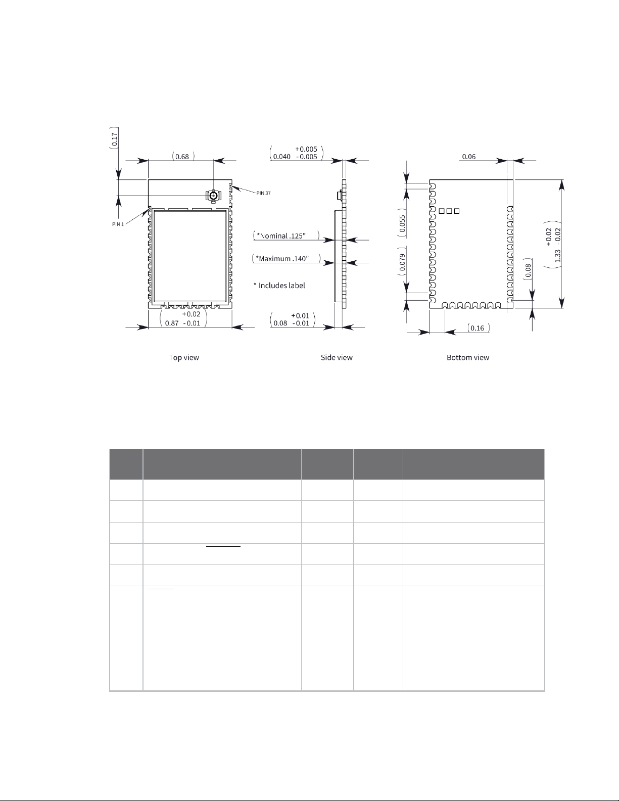
The following mechanical drawings of the XBee 868LP RF Modules show all dimensions in inches.
Antenna options are not shown.
Pin signals
The following table describes the pin assignments for the devices. A horizontal line above the signal
name indicates low-asserted signals.
Pin# Name Direction
1 GND - - Ground
2 V
3 DIO13 / DOUT Both Output GPIO/UART Data Out
4 DIO14 / DIN / CONFIG Both Input GPIO/UART Data In
5 DIO12 Both GPIO
6 RESET Input Module reset. Drive low to
DD
Default
state Description
- - Power supply
reset the module. This is also
an output with an open drain
configuration with an internal
20 kW pull-up (never drive to
logic high, as the module may
be driving it low). The minimum
pulse width is 1 mS.
XBee 868LP RF Modules User Guide
20
Page 21

Hardware Pin signals
Default
Pin# Name Direction
7 DIO10 / RSSI PWM0 Both Output GPIO/RX Signal Strength
8 DIO11 / PWM1 Both Disabled GPIO/Pulse Width Modulator
9 [reserved] - Disabled Do not connect
10 DIO8 / SLEEP_REQUEST Both Input GPIO/Pin Sleep Control Line
11 GND - - Ground
12 DIO19 / SPI_ATTN Output Output
13 GND - - Ground
14 DIO18 / SPI_CLK Input Input GPIO/Serial Peripheral
state Description
Indicator
(DTR on the dev board)
Serial Peripheral Interface
Attention or UART Data
Present indicator
Interface Clock/
15 DIO17 / SPI_SSEL/ Input Input GPIO/Serial Peripheral
Interface not Select
16 DIO16 / SPI_MOSI Input Input GPIO/Serial Peripheral
Interface Data In
17 DIO15 / SPI_MISO/ Output Output GPIO/Serial Peripheral
Interface Data Out
Tri-stated when SPI_SSEL is
high
18 [reserved]* - Disabled Do not connect
19 [reserved]* - Disabled
20 [reserved]* - Disabled
21 [reserved]* - Disabled
22 GND - - Ground
23 [reserved] - Disabled Do not connect
24 DIO4 Both Disabled GPIO
25 DIO7 / CTS/ Both Output GPIO/Clear to Send Flow
Do not connect
Do not connect
Do not connect
Control
26 ON/SLEEP/DIO9 Both Output GPIO/Module Status Indicator
XBee 868LP RF Modules User Guide
21
Page 22

Hardware Design notes
Default
Pin# Name Direction
27 VREF Input -
28 DIO5 / ASSOCIATE/ Both Output GPIO/Associate Indicator
29 DIO6 / RTS Both Input GPIO/Request to Send Flow
30 DIO3 / AD3 Both Disabled GPIO/Analog Input
state Description
Not used internally. Used for
programmable secondary
processor. For compatibility
with other XBee modules, we
recommend connecting this
pin to the voltage reference if
Analog Sampling is desired.
Otherwise, connect to GND.
Control
31 DIO2 / AD2 Both Disabled
32 DIO1 / AD1 Both Disabled
33 DIO0 / AD0 Both Input GPIO/Analog Input
34 [reserved] - Disabled Do not connect
35 GND - - Ground
36 RF Both - RF I/O for RF Pad Variant
37 [reserved] - Disabled Do not connect
Signal Direction is specified with respect to the device.
See Design notes for details on pin connections.
* These pins are not available for customer use.
Design notes
The XBee modules do not require any external circuitry or specific connections for proper operation.
However, there are some general design guidelines that we recommend to build and troubleshoot a
robust design.
GPIO/Analog Input
GPIO/Analog Input
Power supply design
A poor power supply can lead to poor radio performance, especially if you do not keep the supply
voltage within tolerance or if the noise is excessive. To help reduce noise, place a 1.0 µF and 47 pF
capacitor as near as possible to pin 2 on the PCB. If you are using a switching regulator for the power
supply, switch the frequencies above 500 kHz. Limit the power supply ripple to a maximum 250 mV
peak to peak.
For designs using the programmable modules, we recommend an additional 10 µF decoupling cap
near pin 2 of the device. The nearest proximity to pin 2 of the three caps should be in the following
order:
XBee 868LP RF Modules User Guide
22
Page 23

Hardware Design notes
1. 47 pf
2. 1 µF
3. 10 µF
Board layout
We design XBee modules to be self-sufficient and have minimal sensitivity to nearby processors,
crystals or other printed circuit board (PCB) components. Keep power and ground traces thicker than
signal traces and make sure that they are able to comfortably support the maximum current
specifications. There are no other special PCB design considerations to integrate XBee modules, with
the exception of antennas.
To view a recommended PCB footprint for the module, see Manufacturing information.
Antenna performance
Antenna location is important for optimal performance. The following suggestions help you achieve
optimal antenna performance. Point the antenna up vertically (upright). Antennas radiate and receive
the best signal perpendicular to the direction they point, so a vertical antenna's omnidirectional
radiation pattern is strongest across the horizon.
Position the antennas away from metal objects whenever possible. Metal objects between the
transmitter and receiver can block the radiation path or reduce the transmission distance. Objects
that are often overlooked include:
n Metal poles
n Metal studs
n Structure beams
n Concrete, which is usually reinforced with metal rods
If you place the device inside a metal enclosure, use an external antenna. Common objects that have
metal enclosures include:
n Vehicles
n Elevators
n Ventilation ducts
n Refrigerators
n Microwave ovens
n Batteries
n Tall electrolytic capacitors
Use the following additional guidelines for optimal antenna performance:
n Do not place XBee modules with the chip antenna inside a metal enclosure.
n Do not place any ground planes or metal objects above or below the antenna.
n For the best results, mount the device at the edge of the host PCB. Ensure that the ground,
power, and signal planes are vacant immediately below the antenna section.
Recommended pin connections
The only required pin connections for two-way communication are VDD, GND, DOUT and DIN. To
support serial firmware updates, you must connect VDD, GND, DOUT, DIN, RTS, and DTR.
XBee 868LP RF Modules User Guide
23
Page 24

Hardware Design notes
Do not connect any pins that are not in use. Use the PR and PD commands to pull all inputs on the
radio high or low with 40k internal pull-up or pull-down resistors. Unused outputs do not require any
specific treatment.
For applications that need to ensure the lowest sleep current, never leave unconnected inputs
floating. Use internal or external pull-up or pull-down resistors, or set the unused I/O lines to outputs.
You can connect other pins to external circuitry for convenience of operation including the Associate
LED pad (pad 28) and the Commissioning pad (pad 33). The Associate LED pad flashes differently
depending on the state of the module to the network, and a pushbutton attached to pad 33 can
enable various join functions without having to send serial port commands. For more information see
Commissioning pushbutton and associate LED. The source and sink capabilities are limited to 6 mA on
all I/O pads.
Only the programmable versions of these devices use the VREF pad (pad 27). For compatibility with
other XBee modules, we recommend connecting this pin to a voltage reference if you want to enable
analog sampling. Otherwise, connect to GND.
Design notes for PCB antenna devices
Position PCB antenna devices so there are no ground planes or metal objects above or below the
antenna. For best results, do not place the device in a metal enclosure, as this may greatly reduce the
range. Place the device at the edge of the PCB on which it is mounted. Make sure the ground, power
and signal planes are vacant immediately below the antenna section.
The following drawings illustrate important recommendations when you are designing with PCB
antenna devices. For optimal performance, do not mount the device on the RF pad footprint described
in the next section, because the footprint requires a ground plane within the PCB antenna keep out
area.
XBee 868LP RF Modules User Guide
24
Page 25
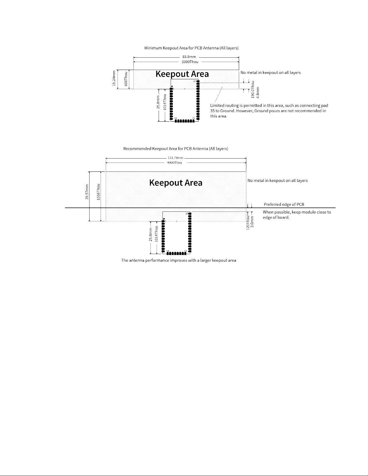
Hardware Design notes
Notes
1. We recommend non-metal enclosures. For metal enclosures, use an external antenna.
2. Keep metal chassis or mounting structures in the keepout area at least 2.54 cm (1 in) from the
antenna.
3. Maximize the distance between the antenna and metal objects that might be mounted in the
keepout area.
4. These keepout area guidelines do not apply for wire whip antennas or external RFconnectors.
Wire whip antennas radiate best over the center of a ground plane.
Design notes for RF pad devices
The RF pad is a soldered antenna connection. The RF signal travels from pin 33 on the device to the
antenna through an RF trace transmission line on the PCB. Any additional components between the
device and antenna violates modular certification. The controlled impedance for the RF trace is 50 Ω.
We recommend using a microstrip trace, although you can also use a coplanar waveguide if you need
more isolation. A microstrip generally requires less area on the PCB than a coplanar waveguide. We do
not recommend using a stripline because sending the signal to different PCB layers can introduce
matching and performance problems.
XBee 868LP RF Modules User Guide
25
Page 26

Hardware Design notes
Following good design practices is essential when implementing the RF trace on a PCB. Consider the
following points:
n Minimize the length of the trace by placing the RPSMA jack close to the device.
n Connect all of the grounds on the jack and the device to the ground planes directly or through
closely placed vias.
n Space any ground fill on the top layer at least twice the distance d (in this case, at least 0.028")
from the microstrip to minimize their interaction.
Additional considerations:
n The top two layers of the PCB have a controlled thickness dielectric material in between.
n The second layer has a ground plane which runs underneath the entire RF pad area. This
ground plane is a distance d, the thickness of the dielectric, below the top layer.
n The top layer has an RF trace running from pin 33 of the device to the RF pin of the RPSMA
connector.
n The RF trace width determines the impedance of the transmission line with relation to the
ground plane. Many online tools can estimate this value, although you should consult the PCB
manufacturer for the exact width.
Implementing these design suggestions helps ensure that the RF pad device performs to its
specifications.
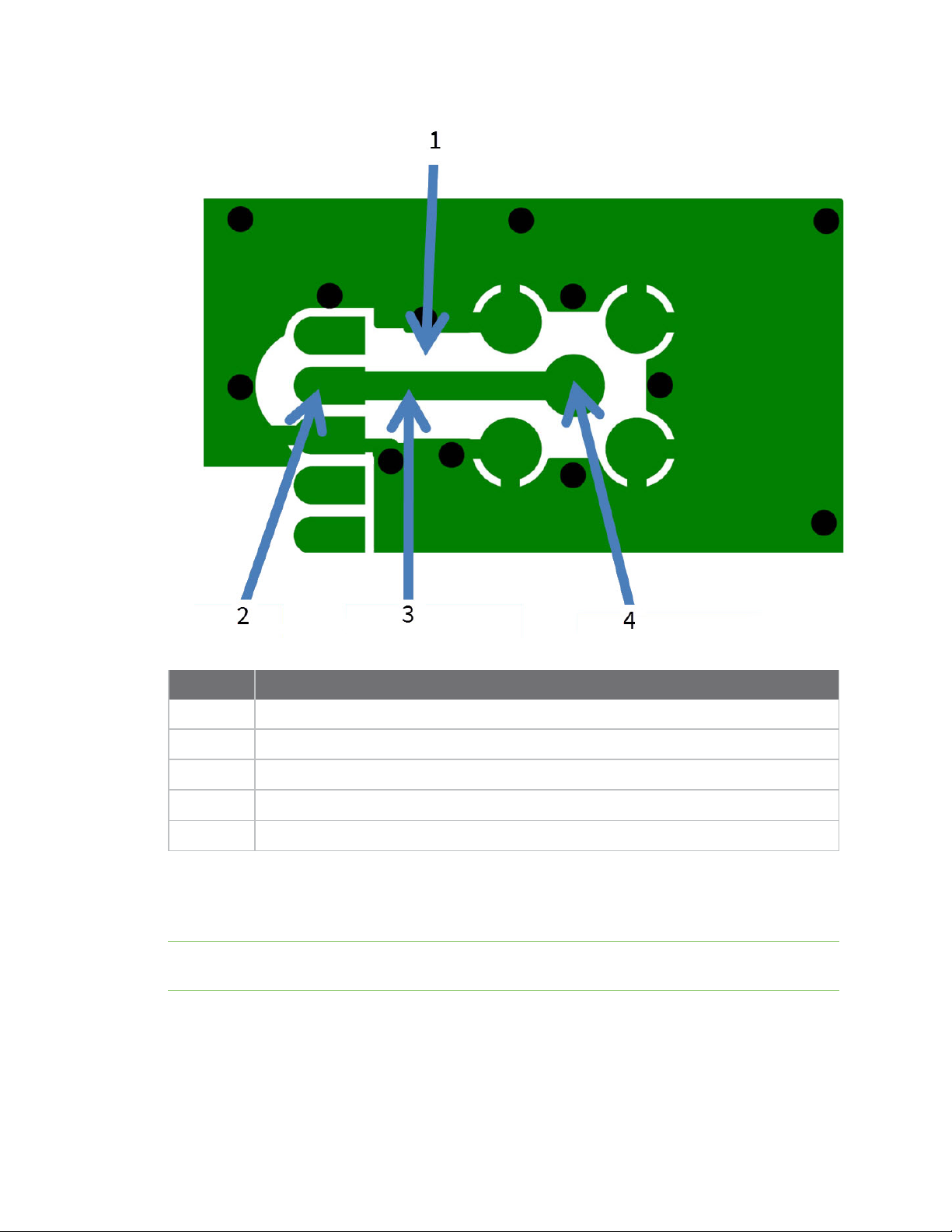
The following figures show a layout example of a host PCB that connects an RF pad device to a right
angle, through-hole RPSMA jack.
XBee 868LP RF Modules User Guide
26
Page 27
Hardware Design notes
Number Description
1
2 Device pin 33.
2 RF pad pin.
3 50 Ω microstrip trace.
4 RF connection of RPSMA jack.
The width in this example is approximately 0.025 in for a 50 Ω trace, assuming d = 0.014 in, and that
the dielectric has a relative permittivity of 4.4. This trace width is a good fit with the device footprint's
0.335" pad width.
Note We do not recommend using a trace wider than the pad width, and using a very narrow trace
(under 0.010") can cause unwanted RF loss.
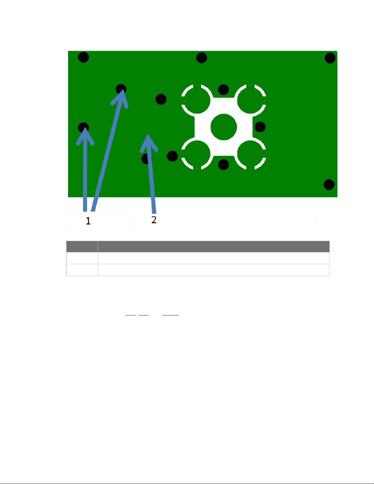
The following illustration shows PCB layer 2 of an example RF layout.
Maintain a distance of at least 2 d between microstrip and ground fill.
XBee 868LP RF Modules User Guide
27
Page 28
Hardware Module operation for the programmable variant
Number Description
1
2 Put a solid ground plane under RF trace to achieve the desired impedance.
Use multiple vias to help eliminate ground variations.
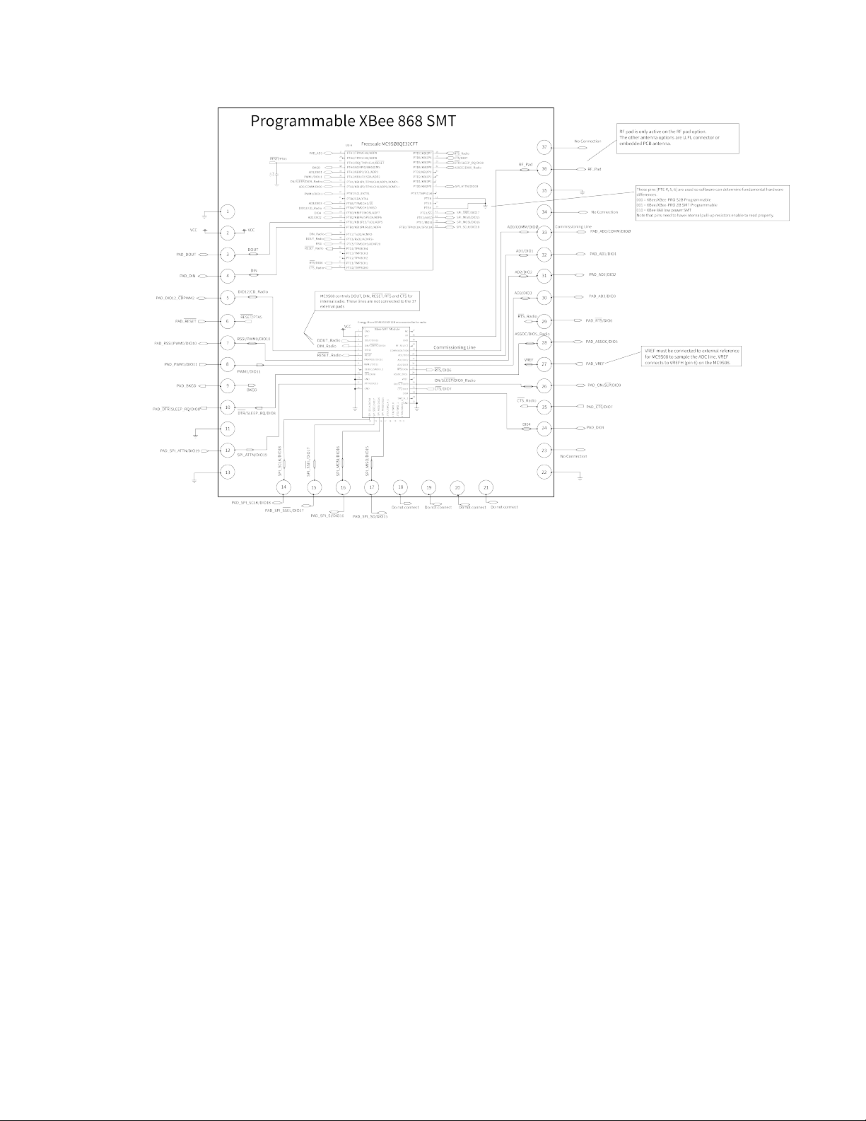
Module operation for the programmable variant
The modules with the programmable option have a secondary processor with 32k of flash and 2k of
RAM. This allows module integrators to put custom code on the XBee module to fit their own unique
needs. The DIN, DOUT, RTS, CTS, and RESET lines are intercepted by the secondary processor to allow
it to be in control of the data transmitted and received. All other lines are in parallel and can be
controlled by either the internal microcontroller or the MC9SO8QE micro; see the block diagram in
Operation for details. The internal microcontroller by default has control of certain lines. The internal
microcontroller can release these lines by sending the proper command(s) to disable the desired DIO
line(s). For more information about commands, see AT commands.
For the secondary processor to sample with ADCs, the XBee must be connected to a reference
voltage.
Digi provides a bootloader that can take care of programming the processor over-the-air or through
the serial interface. This means that over-the-air updates can be supported through an XMODEM
protocol. The processor can also be programmed and debugged through a one wire interface BKGD .
XBee 868LP RF Modules User Guide
28
Page 29
Hardware Programmable XBee SDK
Programmable XBee SDK
The XBee Programmable module is equipped with a NXP MC9S08QE32 application processor. This
application processor comes with a supplied bootloader. To interface your application code running on
this processor to the XBee Programmable module's supplied bootloader, use the Programmable XBee
SDK.
To use the SDK, you must also download CodeWarrior. The download links are:
n CodeWarrior IDE: http://ftp1.digi.com/support/sampleapplications/40003004_B.exe
n Programmable XBee SDK: http://ftp1.digi.com/support/sampleapplications/40003003_D.exe
If these revisions change, search for the part number on Digi’s website. For example, search for
40003003.
Install the IDE first, and then install the SDK.
The documentation for the Programmable XBee SDK is built into the SDK, so the Getting Started guide
appears when you open CodeWarrior.
XBee 868LP RF Modules User Guide
29
Page 30

Get started
The XBee 868LP RF Modules support low-power, peer-to-peer or wireless mesh networks for Europe
(868 MHz). The XBee 868LP RF Modules provide reliable delivery of data between remote devices.
This guide shows you how to set up a mesh network using the DigiMesh protocol, send data between
devices, and adjust XBee 868LP RF Module settings.
Note For more information about DigiMesh protocol and features, see DigiMesh networking.
This guide covers the following tasks and features:
Set up the devices 31
Do more with your XBee modules 47
Learn more about XBee module features 58
Troubleshooting 59
XBee 868LP RF Modules User Guide
30
Page 31

Get started Set up the devices
Set up the devices
Before you begin
To get started with your XBee RF module development kit, verify that your kit has all of the
components and that you meet the system requirements.
Verify kit contents
The XBee 868LP RF Module development kit contains the following components:
XBee
U.FLmodule (3)
XBee
development
board (3)
USB cable (2)
Power supply
(2)
Set of power
supply adapters
(2)
XBee 868LP RF Modules User Guide
31
Page 32

Get started Set up the devices
Antenna U.FL (3)
Gather required materials
To complete the steps in this guide, you need the following items:
Item
Computer
XCTU
software
Description
Operating systems:
n Windows Vista/7/8 (32-bit or 64-bit versions)
n Mac OS X v10.6 and higher versions (64-bit only)
n Linux with KDE or GNOME window managers (32-bit or 64-bit versions)
System requirements:
n HDD space: 500 MB minimum, 1GB recommended
n RAM memory: 2 GB minimum, 4 GB recommended
n CPU: Dual-core processor minimum, Quad-core processor recommended
USB ports:
n Three available USB ports for the XBee/XBee-PRO DigiMesh 2.4 development kit
n Two available USB ports for the XBee 868LP development kit
Note Only one computer is required to follow along with the steps in this guide.
However, you can use two or more computers—one for each XBee module. For range
testing, we recommend a laptop.
Version 6.1.3 or later. See Download and install XCTU.
USB
drivers
Windows Vista and later: USB drivers automatically install through plug-and-play.
Windows XP and earlier: You need to download the driver software.
See Optional: Manually install USB drivers.
Connect the hardware
The following illustration shows you how to assemble the hardware components of the development
kit.
XBee 868LP RF Modules User Guide
32
Page 33

Get started Set up the devices
1. Attach the XBee 868LP RF Modules to the development boards.
2. Attach the antennas to the devices.
3. Connect the USB cables to the development boards.
CAUTION! Before you remove a device from a development board, make sure the board is
not powered by a USB cable or a battery.
Step 1: Download and install XCTU
This section contains download and install instructions based on operating system. XCTU is
compatible with Linux, OSX, and Windows. It may be necessary to configure your system prior to
installing XCTU for the first time.
If you get stuck, see XCTU installation error.
XBee 868LP RF Modules User Guide
33
Page 34

Get started Set up the devices
Download and install XCTU - Windows
Follow the steps below to download and install XCTU on your computer.
1. Go to www.digi.com/xctu.
2. Click Download.
3. Under Download XCTU, click the Windows installer link.
4. Once the download is complete, run the executable file and follow the steps in the XCTU Setup
Wizard.
Once installation is complete, a “What’s new” dialog appears where you can review the new
XCTU features.
Download and install XCTU - Linux
By default, access to the serial and USB ports in Linux is restricted to root and dialout group users. To
access your XBee devices and use XCTU to communicate with them, it is mandatory that your Linux
user belongs to this group. To add your Linux user to the dialout group:
1. Open a terminal console.
2. Execute the following command where <user> is the user you want to add to the dialout group:
sudo usermod -a -G dialout <user>
3. Log out and log in again with your user in the system.
4. Go to www.digi.com/xctu.
5. Click Download.
6. Under Download XCTU, click the Linux installer link.
7. Once the download is complete, run the executable file and follow the steps in the XCTU Setup
Wizard.
Once installation is complete, a “What’s new” dialog appears where you can review the new
XCTU features.
Download and install XCTU - OSX
OSX version 10.8 (Mountain Lion) and greater only allows you to install applications downloaded from
the Apple Store. To install XCTU, you must temporarily disable this setting. Follow these steps to
enable installation of "unsigned" software:
1. Click the Apple icon in the top-left corner of your screen and choose System Preferences.
2. Click the Security & Privacy icon.
3. To edit security settings, click the padlock icon in the bottom left of the window.
4. Enter your Mac credentials and click Unlock. The Allow applications downloaded from dialog
appears.
5. Click the Anywhere radio button and, in the confirmation window, click Allow From
Anywhere.
Note We recommend you set this option back to Mac App Store or Mac App Store and identified
developers once you have finished installing XCTU.
XBee 868LP RF Modules User Guide
34
Page 35

Get started Set up the devices
6. Go to www.digi.com/xctu.
7. Click Download.
8. Under Download XCTU, click the OSX installer link.
9. Once the download is complete, unzip and run the executable file and follow the steps in the
XCTU Setup Wizard.
Once installation is complete, a “What’s new” dialog appears where you can review the new
XCTU features.
Optional: Install XCTU updates
When you start XCTU, you may be notified about software updates. You should always run the latest
version of XCTU.
1. When a new version is available, a popup window appears in the bottom-right corner of XCTU.
2. Click on that window and follow the prompts to proceed with the update.
You can also check for updates and manually update the tool by clicking Help > Check for XCTU
Updates.
Optional: Manually install USB drivers
When you connect the XBee board to your computer for the first time, drivers are automatically
installed. You can also install device drivers manually:
1. Download and install the appropriate USB drivers from the Digi Support Site.
2. Choose your operating system.
3. Download and run the file.
4. Follow the steps in the installation wizard.
Step 2: Set up your first wireless connection
This section shows you how to configure two XBee modules in AT (transparent) mode. The XBee
module passes information along exactly as it receives it. All serial data received by the XBee module
is sent wirelessly to a remote destination XBee module.
If you get stuck, see Troubleshooting.
Add devices to XCTU
These instructions show you how to add two devices to XCTU. However, you can use these
instructions to add any number of devices.
1. Connect two XBee 868LP RF Modules to your computer using the USB cables.
Tip Connect the two shorter range XBee modules instead of the longer range XBee-PRO
modules. This will make it easier to set up a mesh network. See Connect the hardware.
2.
Launch XCTU .
3.
Click the Configuration working modes button .
4.
Click the Discover radio modules button .
XBee 868LP RF Modules User Guide
35
Page 36

Get started Set up the devices
5. In the Discover radio devices dialog, select the serial ports where you want to look for devices
and click Next.
6. In the Set port parameters window, maintain the default values and click Finish.
As XCTU locates devices, they appear in the Discovering radio modules dialog box.
7. Click Add selected devices once the discovery process has finished.
You should see something like this in the Radio Modules section:
Configure the first two devices in Transparent mode
To transmit data wirelessly between your XBee devices, configure them to be in the same network.
Tip To locate a device, select it in XCTU and click the Read radio settings button . The Rx and Tx
LED lights on its development board blink green and yellow.
Set up the first XBee device (XBEE_A)
1. Select the first XBee device.
2.
Click the Load default firmware settings button .
Tip In the following steps, type parameter letters in the Search box to
quickly find a parameter.
3. Configure the following parameters:
ID:2015
DH: 0013A200
XBee 868LP RF Modules User Guide
36
Page 37

Get started Set up the devices
DL: SL of XBEE_B (Enter the last eight characters of the MAC address for XBEE_B. Or select
XBEE_Band find its SL value.)
NI:XBEE_A
4.
Click the Write radio settings button .
Set up the second XBee device (XBEE_B)
1. Configure the following parameters:
ID:2015
DH: 0013A200
DL: SL of XBEE_A (Enter the last eight characters of the MAC address for XBEE_A. Or select
XBEE_Aand find its SL value.)
NI:XBEE_B
2.
Click the Write radio settings button .
After you write the radio settings for the XBee devices, their names appear in the Radio Modules
area.
For more information about the parameters, see the following table:
Parameter XBEE_A XBEE_B Effect
ID 2015 2015 Defines the network that a device will attach to. This must be
the same for all devices in your network.
DH 0013A200 0013A200 Defines the destination address (high part) for the message.
DL
NI XBEE_A XBEE_B
SL
of
XBEE_B
SL
of
XBEE_A
Defines the destination address (low part) for the message.
The value of this setting is the Serial Number Low (SL) of the
other XBee device.
Defines the node identifier.
Note The default NI value is a blank space. Delete the space
when you change the value.
Check the network
Once both XBee 868LP RF Modules are configured, use XCTU to check that they are in the same
network and can see each other.
XBee 868LP RF Modules User Guide
37
Page 38

Get started Set up the devices
1.
Click the Discover radio nodes in the same network button of XBEE_A.
The XBee 868LP RF Module searches for radio modules in the same network.
When the discovery process is finished, XCTU lists discovered devices found within the network
in the Discovering remote devices dialog.
2. Click Cancel. There is no need to add the remote device that has been discovered.
Send messages through XCTU
Use the XCTU console to have the two devices send messages to each other.
1.
Switch both XBee 868LP RF Modules to the consoles working mode .
2. Open a serial connection for each XBee.
a.
Select XBEE_A and click .
b.
Select XBEE_B and click .
3.
Click the Detach view button to see both consoles at the same time.
a. In the Console log area for XBEE_A, type "Hello XBEE_B!"
b. In the Console log area for XBEE_B, type "Hello XBEE_A!"
The message of the sender is in blue font, and the message of the receiver is in red font.
XBee 868LP RF Modules User Guide
38
Page 39

Get started Set up the devices
4. Close the window for XBEE_B.
5.
Keep the serial connections open for both XBee modules.
If the two XBee 868LP RF Modules are unable to talk to each other:
n Verify that you accurately configured the parameters. See Configure the first two devices in
Transparent mode.
n Verify that the following parameters are configured appropriately:
l XBee/XBee-PRO DigiMesh 2.4: The CH (Operating Channel) is the same for both XBee
modules.
l XBee 868LP: The CM (Channel Mask) and HP (Preamble ID) are the same for both XBee
modules.
Step 3: Create a mesh network
This section describes how to add a third XBee module to create a mesh network. Establish a mesh
network any time you want to create a network that is larger than the range of each individual radio.
In these instructions, you first connect a loopback jumper to an XBee module in preparation for
testing your network.
If you get stuck, see Troubleshooting.
Connect a loopback jumper to an XBee device
Connecting a loopback jumper to an XBee device lets you send a message to another XBee device and
have the message loop back to the sender.
XBee 868LP RF Modules User Guide
39
Page 40

Get started Set up the devices
1. Connect the loopback jumper on XBEE_B so it bridges the two pins on its development board.
2.
In the XBEE_A console, click the Clear session button to clear your previous conversation.
3. Type Hello!
Each character loops back in the XBEE_A console log, which indicates that XBEE_Asuccessfully
sent the message to XBEE_B.
You are now ready to use the loopback jumper to help you test a mesh network consisting of
three XBee devices.
Set up a third XBee module to create a mesh network
To create a mesh network, move XBEE_B away from XBEE_A until communication is lost; then add
XBEE_C to relay messages between XBEE_A and XBEE_B. The network automatically adjusts and
redirects communications as soon as a pathway becomes available.
1. Move XBEE_B out of range of XBEE_A:
a. Disconnect XBEE_B from your computer and remove it from XCTU.
b. Connect XBEE_B to a power supply (or laptop or portable battery) and move it away from
XBEE_A until it is out of range.
The approximate indoor range is 500 ft (150 m), and the approximate outdoor range is 2.5
miles (4 km).
XBee 868LP RF Modules User Guide
40
Page 41

Get started Set up the devices
c. Make sure the loopback jumper is connected to XBEE_B. See Connect a loopback jumper
to an XBee device.
d.
In the XBEE_A console, click to clear your previous conversation with XBEE_B.
e. Type "Are you out of range?" In the illustration below, the message does not loop back,
which means XBEE_B did not receive it and it is out of range of XBEE_A.
f. If the message loops back, move XBEE_B farther away until it no longer loops back.
2. Add and configure another XBee module:
a. Connect another XBee module to your computer.
b.
Click the Configuration working modes button .
c.
Click the Add a radio module button .
d. In the Add a radio module dialog, select the USB Serial Port for this XBee module and
click Finish.
e. Configure this XBee module as follows:
ID: 2015
NI: XBEE_C
XBee 868LP RF Modules User Guide
41
Page 42

Get started Set up the devices
f.
Click the Write radio settings button .
3. Have XBEE_C relay messages between XBEE_A and XBEE_B:
a.
Switch back to the Consoles working mode .
b. Disconnect XBEE_C from your computer and remove it from XCTU.
c. Connect XBEE_C to a power supply (or laptop or portable battery) and place it between
XBEE_A and XBEE_B.
d. Make sure the loopback jumper is still connected to XBEE_B.
e. Have XBEE_A send a message to XBEE_B. In the XBEE_A console, type "Hello!"
In the following illustration, the message loops back. XBEE_C relayed your message to XBEE_B,
and you successfully established a mesh network.
Tip Use the Send a single packet command to send and have an entire message loop back,
instead of having individual characters loop back. To do this, click the Add new packet button
to compose your message, and then click Send selected packet to send your message.
Before you perform other tasks, change the loopback jumper on XBEE_B so it no longer
bridges the two pins on its development board. It should look like this:
XBee 868LP RF Modules User Guide
42
Page 43

Get started Set up the devices
Step 4: Use API mode to talk to XBee modules
This section shows you how to configure an XBee module in API mode, which gives you flexibility,
speed, and reliability in your data transmissions.
If you get stuck, see Troubleshooting.
For more information on API mode, see Operate in API mode.
Configure a device in APImode
1.
Select XBEE_A and click the Configuration working modes button .
2. Add this configuration:
AP: API Mode 1
3.
Click the Write radio settings button .
The Port indicates XBEE_A is in API mode.
Send an API Tx frame from an XBee module to another module
API Tx frames are the instructions that allow one XBee module to send data to another XBee module.
In these instructions, XBEE_A uses the API frame type "Transmit Request" to send some text data to
XBee 868LP RF Modules User Guide
43
Page 44

Get started Set up the devices
XBEE_B.
1. Reconnect XBEE_B to your computer.
2. Make sure the loopback jumper on XBEE_B no longer bridges the two pins on its development
board.
3. In XCTU,rediscover XBEE_B.
4. Switch XBEE_A and XBEE_B to console mode:
a.
Select XBEE_A and click . Then click to open a serial connection.
b.
Select XBEE_B and click . Then click to open a serial connection.
5. Select XBEE_A.
6.
In the Send a single frame area, click the Add new frame to the list button .
7. In the Add API frame to the list dialog, click the Create frame using 'Frames Generator'
tool button.
XBee 868LP RF Modules User Guide
44
Page 45

Get started Set up the devices
8. In the XBee API Frame generator dialog, configure the following parameters:
Protocol: DigiMesh
Mode: API 1
Frame type:0x10 - Transmit Request
64-bit dest. address: MAC address of XBEE_B
RF data: Type "Hello XBee_B!" in the ASCII tab
9. Click OK.
10. In the Add API frame to the list dialog, type a name for your frame.
XBee 868LP RF Modules User Guide
45
Page 46

Get started Set up the devices
11. Click Add frame.
12. In the Send frames area, make sure your frame is selected.
13. In the Send a single frame area, click Send selected frame.
14. In the Frames log area, select Transmit Request and then Transmit Status to look at the
Frame details for each.
For example, select Transmit Status and scroll down in the Frame details area to see that
your Delivery status is a success.
XBee 868LP RF Modules User Guide
46
Page 47

Get started Do more with your XBee modules
15. In the Radio Modules area, select XBEE_B. "Hello XBee_B!" should appear in the Console log.
Do more with your XBee modules
Update the firmware
Radio firmware is the program code stored in the radio module's persistent memory that provides the
control program for the device. Use XCTU to update the firmware.
1.
Click the Configuration working modes button .
2. Add local and remote XBee modules to your computer. See Add devices to XCTU and Configure
remote devices.
3. Select a local or remote XBee module from the Radio Modules list.
4.
Click the Update firmware button .
The Update firmware dialog displays the available and compatible firmware for the selected
XBee module.
XBee 868LP RF Modules User Guide
47
Page 48

Get started Do more with your XBee modules
5. Select the product family of the XBee module, the function set, and the latest firmware version.
6. Click Update. A dialog displays update progress.
Configure remote devices
You can communicate with remote devices over the air through a corresponding local device.
Configure the local device in API mode because remote commands only work in API mode. Configure
remote devices in either API or Transparent mode.
These instructions show you how to configure the LT (Associate LED Blink Time) parameter on a
remote device.
1. Add two XBee devices to XCTU. See Add devices to XCTU.
2. Configure the first device in APImode and name it XBEE_A. See Configure a device in
APImode.
3. Configure the second device in either API or Transparent mode, and name it XBEE_B. See
Configure the first two devices in Transparent mode.
4. Disconnect XBEE_B from your computer and remove it from XCTU.
5. Connect XBEE_B to a power supply (or laptop or portable battery).
The Radio Modules area should look something like this.
XBee 868LP RF Modules User Guide
48
Page 49

Get started Do more with your XBee modules
6.
Select XBEE_A and click the Discover radio nodes in the same network button .
7. Click Add selected devices in the Discovering remote devices dialog. The discovered remote
device appears below XBEE_A.
8. Select the remote device XBEE_B, and configure the following parameter:
LT: FF (hexidecimal representation for 2550 ms)
9.
Click the Write radio settings button .
The remote XBee device now has a different LED blink time.
10. To return to the default LED blink times, change the LT parameter back to 0 for XBEE_B.
Set up and perform a range test
This section shows you how to set up two XBee modules to perform a range test, which demonstrates
the real-world RF range and link quality between two XBee modules in the same network. Performing
a range test gives an initial indication of the expected communication performance of the kit
components. When deploying an actual network, perform multiple range tests to analyze varying
conditions in your application.
Configure the devices for a range test
For devices to communicate with each other, you configure them so they are in the same network.
You also set the local device to API mode to obtain all possible data of the remote device.
XBee 868LP RF Modules User Guide
49
Page 50

Get started Do more with your XBee modules
1. Add two devices to XCTU. See Add devices to XCTU.
2.
Select the first device and click the Load default firmware settings button .
3. Configure the following parameters:
ID: 2015
NI: XBEE_A
AP: API enabled [1]
4.
Click the Write radio settings button .
5.
Select the other device and click .
6. Configure the following parameters:
ID: 2015
NI: XBEE_B
AP: API disabled [0]
7.
Click the Write radio settings button .
After you write the radio settings for each device, their names appear in the Radio Modules
area. The Port indicates XBEE_A is in API mode.
8. Disconnect XBEE_B from the computer and remove it from XCTU.
9. Connect XBEE_B to a power supply (or laptop or portable battery) and move it away from
XBEE_A to the desired location for the range test.
The approximate indoor range is 500 ft (150 m), and the approximate outdoor range is 2.5
miles (4 km).
XBee 868LP RF Modules User Guide
50
Page 51

Get started Do more with your XBee modules
Perform a range test
These instructions show you how to use the loopback cluster (0x12) when performing a range test.
The benefit of using this type of range test is you don't have to close the loopback jumper of the
remote module and the module can work in any operating mode.
1.
In XCTU, open the Tools menu and select the Range Test option.
The Radio Range Test window opens. Your local device appears on the left side of the Device
Selection area.
2.
Select XBEE_A and click the Discover remote devices button .
The discovery of remote devices starts. When the discovery process finishes, the other device
(XBEE_B) appears in the Discovering remote devices dialog.
3. Click Add selected devices.
4. Select XBEE_B from the Discovered device drop-down menu in the Device Selection area.
5. For Range Test type, select Cluster ID 0x12.
6.
Click the Start Range Test button .
7. If a notification dialog asks you to close the loopback jumper in the remote device, click OK.
8. Test the signal interference by doing one of the following:
n Place your hands over one of the XBee modules.
n Block line-of-sight with your body.
n Place a metal box over an XBee module.
n Move the remote XBee module to a different room or floor of the building.
The Received Signal Strength Indicator (RSSI) value will decrease and some packets may even
be lost.
XBee 868LP RF Modules User Guide
51
Page 52

Get started Do more with your XBee modules
9. XCTU represents the retrieved data as follows:
n Range Test charts represent the RSSI values of the local and remote devices during the
range test session. The chart also shows the percentage of total packets successfully
sent.
n Local and Remote bar graphs represent the signal strengths of the local and remote
XBee modules. These values are retrieved for the last packet sent/received. RSSI is
measured in dBm. A greater negative value in dBm indicates a weaker signal. Therefore,
-50 dBm is better than -60 dBm.
n Packets sent and Packets received areas show the total number of packets sent,
packets received, transmission errors, and packets lost. The percentage bar graph
indicates the percentage of packets that are successfully sent and received during a
range test session.
In the following illustration, the percentage of packets successfully sent is 69% and received is
64%. The actual percentage of packets successfully sent or received may be higher.
10.
Click the Stop Range Test button to stop the process at any time.
11. When you have completed the range test, remove the remote XBee modules from XCTU by
clicking the Remove the list of remote modules button .
Configure basic synchronous sleep support
This section shows you how to extend the battery life of an XBee device and demonstrates how a
DigiMesh network handles messages when nodes are synchronously sleeping. You will configure one
of the devices as a sleep support node and the other two as synchronous cyclic sleep nodes.
The sleep support XBee device is always awake and can receive serial or over-the-air data at any time,
whereas the synchronized sleeping devices cannot send or receive data during their sleep periods.
When receivers are asleep, the messages are buffered and forwarded to their destination once they
XBee 868LP RF Modules User Guide
52
Page 53

Get started Do more with your XBee modules
have woken up. In either case, XBee devices can only receive data up to the capacity of the input
buffer.
Configure the sleep coordinator for synchronous sleep support
These instructions show you how to configure XBEE_A as the preferred sleep coordinator so it stays
awake while the other XBee devices sleep. You then configure XBEE_B and XBEE_C so one of them
assumes the role of sleep coordinator when you disconnect XBEE_A. This allows the network to
remain in sync with minimal impact on battery life.
Note If you have only two USB cables: After you configure XBEE_B, disconnect it from your computer
and remove it from XCTU. Then connect it to a power supply (or laptop or portable battery). Next, use
the available USB cable to connect and configure XBEE_C.
1. Add three devices to XCTU. See Add devices to XCTU.
2.
For each device, click the Load default firmware settings button and then the Write
radio settings button .
3. Configure the three XBee devices in either Transparent or API mode. This example configures
the XBee devices in Transparent mode.
4. Select XBEE_A and configure the following parameters:
SM: 7
SO: 1 (preferred sleep coordinator)
SP: 1F4 (hexidecimal) = 500 (decimal) x 10 ms = 5 seconds
ST: 1388 (hexidecimal) = 5000 (decimal) x 1ms = 5 seconds
XBee 868LP RF Modules User Guide
53
Page 54

Get started Do more with your XBee modules
5.
Click the Write radio settings button .
Note The SP (sleep time) and ST (wake time) are set to five seconds to make it easy to observe
synchronous sleep support. To simulate a sensor system such as water monitoring, you might
set SPto 30 minutes and STto 10 seconds, depending on the number of devices and amount of
data that is transferred.
6. Select XBEE_B and configure the following sleep parameters:
SM: 8
SO: 0 (allows the XBee module to take over the role of sleep coordinator if the preferred sleep
coordinator fails)
SP: 1E (hexidecimal) = 30 (decimal) x 10 ms = 300 ms
ST: BB8 (hexidecimal) = 3000 (decimal) x 1 ms = 3 seconds
7.
Click the Write radio settings button .
8.
Configure the sleep parameters for XBEE_C as you did for XBEE_B. Click when you are
done.
Note Once XBEE_B and XBEE_C sync up to the network, their wake and sleep times are
controlled by the OS and OW settings on the sleep support node (XBEE_A). If you want to
change the wake and sleep times, change the SP and STvalues for XBEE_A.
XBee 868LP RF Modules User Guide
54
Page 55

Get started Do more with your XBee modules
9. The LEDlights on the three devices appear as follows:
XBee module Wake period Sleep period
XBEE_A (sleep coordinator) Flashing red light Solid red light
XBEE_B and XBEE_C Flashing red light No light
10. Change the role of sleep coordinator:
a. Disconnect XBEE_A from your computer.
b. Observe XBEE_B or XBEE_C taking over the role of sleep coordinator by looking at the
behavior of the LEDlights. It could take three cycles for the new sleep coordinator to take
effect.
c. Re-connect XBEE_Ato your computer.
d. Observe XBEE_A re-assuming the role of sleep coordinator.
Note If a device gets out of sync, it goes through a re-synchronization process.
Observe flow control during synchronous sleep support
These instructions demonstrate the importance of observing flow control while XBees are sending
and receiving data during synchronous sleep support. Flow control is the process used by a device to
inform another device to stop sending data in order to prevent data loss.
1.
Click the Consoles working mode button .
2.
Select XBEE_A (the preferred sleep coordinator), and click to open a serial connection.
3.
Select XBEE_B and click .
4.
Click the Detach view button to see both consoles at the same time.
5. In the Console log area for XBEE_A, type "Hello XBee_B! It is Friday! How are you?"
Note All XBee DigiMesh modules have a CTS pin (pin 12) that can inform a connected processor
when it is permissible to send data to the XBee module. In XCTU, the CTS icon indicates
whether an XBee module is awake (the icon is highlighted) or asleep (the icon is not
highlighted).
Since XBEE_A is the sleep coordinator, it transmits its entire message to XBEE_B. The CTSicon
for XBEE_A stays on the entire time.
XBee 868LP RF Modules User Guide
55
Page 56

Get started Do more with your XBee modules
6. In the Console log area for XBEE_B, type "Hello XBee_A! It is Friday! How are you?"
Since XBEE_B is a synchronized sleeping module, it only transmits the part of the message that
is typed while it is awake. In the illustration below, it was only able to transmit "Hello XBee_
A!"The CTSicon for XBEE_B turned off after this part of the message was typed.
XBee 868LP RF Modules User Guide
56
Page 57

Get started Do more with your XBee modules
7.
To disconnect, click the Close serial connection button for each console.
Set up basic encryption for an XBee network
The information transmitted in an XBee network sometimes needs to be protected. For example, an
XBee network transferring financial information must be carefully protected against external agents.
These instructions show you how to configure XBee 868LP RF Modules for secure communication via
encryption keys.
Note You can use encryption for devices that have been configured for either Transparent or API
mode.
1. Add two XBee modules to XCTU. See Add devices to XCTU.
2. Configure the XBee modules so they can talk to each other. See Configure the first two devices
in Transparent mode.
3. Name your two XBee modules XBee_A and XBee_B.
4. Select XBee_A and configure the following parameters:
EE: Set the AES Encryption Enable parameter to 1.
KY: Set the AES Encryption Key parameter to a 32 hexadecimal character string. Example:
11111222223333344444555556666677
XBee 868LP RF Modules User Guide
57
Page 58

Get started Learn more about XBee module features
5.
Click the Write radio settings button .
6.
Configure the parameters for XBEE_B as you did for XBEE_A, and then click .
7. Send a secure message between XBee_A and XBee_B. See Send messages through XCTU.
Note If you add more devices, give them the same encryption key so they can communicate with the
other XBee devices.
8. To return to the encryption disabled setting, change the EEparameter back to 0 for XBEE_A
and XBEE_B.
Learn more about XBee module features
For more information about XBee 868LP RFmodules, see the XBee 868LP RF Modules User Guide. You
can find this guide on the Digi Support site.
Unicast versus broadcast transmissions
An XBee module can communicate with multiple devices or with just one device:
n Broadcast transmissions are sent to many or all XBee modules in the network.
n Unicast transmissions route wireless data from one XBee module to another specific XBee
module.
Broadcast transmission
A broadcast transmission transmits the same data to all nodes on the network. These transmissions
are propagated throughout the entire network so that all possible nodes receive the transmission.
An example of broadcast communication is a television station.
Unicast transmission
A unicast transmissionsends messages to a single node on the network that is identified by a unique
64-bit address. The destination XBee module could be an immediate neighbor of the sender, or be
several hops away.
An example of a unicast communication is a telephone call between two people.
For more information, see Data transmission and routing.
Analog inputs and digital inputs and outputs
All XBee modules have a set of pins that can be used to connect sensors or actuators and configure
them for specific behavior. Each XBee module has the capability to directly gather sensor data and
transmit it without the use of an external microcontroller.
With these pins you can, for example, turn on a light by sending information to an XBee module
connected to an actuator, or measure the outside temperature by obtaining data from a temperature
sensor attached to your XBee module.
XBee 868LP RF Modules User Guide
58
Page 59

Get started Troubleshooting
Sleep modes
Putting XBee devices into a temporary sleep state preserves battery life when using wireless
networks. DigiMesh devices support five sleep modes that are classified as synchronous or
asynchronous. For more information about using sleep modes, see Sleep modes.
Note Asynchronous sleep modes should not be used in a synchronous sleeping network, and vice
versa.
Transparent and API operating modes
The firmware operates in several different modes. Two top-level modes establish how the device
communicates with other devices through its serial interface: Transparent operating mode and API
operating mode.
Transparent operating mode
Devices operate in this mode by default. We also call this mode “AT operating mode.” The device acts
as a serial line replacement when it is in Transparent operating mode. The device queues all of UART
data it receives through the DIN pin for RF transmission. When a device receives RF data, it sends the
data out through the DOUT pin. You can set the configuration parameters using the AT Command
interface.
API operating mode
API operating mode is an alternative to Transparent mode. API mode is a frame-based protocol that
allows you to direct data on a packet basis. It can be particularly useful in large networks where you
need to control the route a data packet takes or when you need to know which node a data packet is
from. The device communicates UART data in packets, also known as API frames. This mode allows for
structured communications with serial devices. It is helpful in managing larger networks and is more
appropriate for performing tasks such as collecting data from multiple locations or controlling
multiple devices remotely.
There are two types of API operating modes: one with escaped characters and another without
escaped characters.
n Without escaped characters. This mode eliminates escaping character sequences. This makes
it simpler to create code and libraries, but runs a minor risk of lost frames or errors due to the
possibility that payload data can be confused with frame structure. We do not recommend this
mode for noisy radio environments and where payload data may include special characters
(specifically 0x7E, 0x7D, 0x11, and 0x13).
n With escaped characters. This mode escapes characters in an API frame in order to improve
the reliability of the RF transmission, especially in noisy environments. API escaped operating
mode (AP = 2) works similarly to API mode. The only difference is that when working in API
escaped mode, the software must escape any payload bytes that match API frame specific
data, such as the start-of-frame byte (0x7E).
Troubleshooting
If you get stuck while performing any of the tasks in this guide, try one of these troubleshooting tips.
Cannot install device driver
Device driver software was not successfully installed.
XBee 868LP RF Modules User Guide
59
Page 60

Get started Troubleshooting
Condition
Sometimes when you connect an XBee module to your computer, the operating system does not
install the driver.
Solution
Try the following, in order. If one of the steps resolves the issue, you're done.
1. Remove and re-insert the XBee module into your computer.
2. If the OS is still unable to install the driver, remove and re-insert the XBee module into another
USB port.
3. Manually install the USB drivers. See Optional: Manually install USB drivers.
Use LEDs to identify XBee modules
You want to force LEDs to blink so you can easily locate an XBee 868LP RF Module.
Resolution
To locate an XBee 868LP RF Module using LEDs:
1.
In XCTU, select one of the devices and click the Read radio settings button .
2. Observe which device has the Rx and Tx LED lights blinking green and yellow on its
development board.
No remote devices to select for a range test
If there are no remote devices to select in the Radio Range Test dialog, try one of the following
resolutions.
Check cables
The USB cables should be firmly and fully attached to both the computer and the development board.
When attached correctly, the association LED on the adapter is illuminated.
Check that the device is fully seated in the development board
When the device is correctly installed, it is pushed fully into the board and no air or metal is visible
between the plastic of the adapter socket and the XBee 868LP RF Module headers. Also, check that all
ten pins on each side of the device are in a matching hole in the socket.
Check the XBee device orientation
The angled "nose" of the XBee 868LP RF Module should match the lines on the silk screening of the
board and point away from the USB socket on the development board.
Check that the devices are in the same network
Check that the following parameters have the same value for all devices on the network:
XBee 868LP RF Modules User Guide
60
Page 61

Get started Troubleshooting
XBee module development kit Parameters
XBee/XBee-PRO DigiMesh 2.4
XBee S2C DigiMesh 2.4
XBee 868LP
ID (Network ID) and CH (Operating Channel)
ID (Network ID) and CH (Operating Channel)
ID (Network ID), HP (Preamble ID), and CM (Channel Mask)
Restore default settings
If the devices are properly connected and in the same network, restore default settings and configure
them again.
Port in use
Message:"The port is already in use by other applications."
Condition
The serial port where the local XBee 868LP RF Module is connected can only be in use by one
application.
Solution
Make sure the connection with the XBee 868LP RF Module in the XCTU console is closed and there are
no other applications using the port.
XCTU cannot discover devices
If XCTU does not discover an XBee device or does not display any serial ports, try the following
resolutions.
Check the configuration of your USB serial converter
1. On the Start menu, click Computer > System Properties > Device Manager.
2. Under Serial Bus controllers, double-click the first USB Serial Converter to open the USB Serial
Converter dialog.
3. Click the Advanced tab, make sure Load VCP is selected, and click OK.
4. Repeat steps 2 and 3 for each USB Serial Converter listed in the Device Manager.
Check cables
Double-check all cables. The USB cable should be firmly and fully attached to both the computer and
the XBee development board. When attached correctly, the association LED on the adapter will be lit.
Check that the XBee module is fully seated in the XBee development board
When the XBee module is correctly installed, it should be pushed fully into the board and no air or
metal should be visible between the plastic of the adapter socket and the XBee module headers. Also,
double-check that all ten pins on each side of the XBee module made it into a matching hole in the
socket.
XBee 868LP RF Modules User Guide
61
Page 62

Get started Troubleshooting
Check the XBee module orientation
The angled "nose" of the XBee module should match the lines on the silk screening of the board and
point away from the USB socket on the XBee development board.
Check driver installation
Drivers are installed the first time the XBee development board is plugged in. If this process is not
complete or has failed, try the following steps:
1. Remove and re-insert the board into your computer. This may cause driver installation to re-
occur.
2. Remove and re-insert the board into another USB port.
3. (Windows) Open Computer management, find the failing device in the Device Manager section
and remove it.
4. Download the appropriate driver. You can download drivers for all major operating systems
from FTDI for manual installation.
Check if the modules are sleeping
The On/Sleep LED of the XBee development board indicates if the XBee module is awake (LED on) or
asleep (LED off). When an XBee module is sleeping, XCTUcannot discover it, so press the
Commissioning button to wake it up for 30 seconds.
XCTUcannot discover remote devices
XCTUdoes not discover remote XBee 868LP RF Module.
Potential cause
The devices do not have the appropriate values for the following parameters:
XBee module development kit Parameters
XBee 868LP
ID (Network ID), HP (Preamble ID), and CM (Channel Mask)
Resolution
1. Ensure that all devices on your network have the same value for each of the parameters listed
in the table.
2. If this does not resolve the issue, try setting your devices back to their default settings. Select
each XBee device and click the Load default firmware settings button .
XCTUcannot discover remote devices for a range test
When setting up a range test in the Radio Range Test dialog, you receive the message "There are not
remote devices discovered for the selected local device."
Condition
In the Radio Range Test dialog, the local radio device you selected has not yet discovered any remote
devices.
XBee 868LP RF Modules User Guide
62
Page 63

Get started Troubleshooting
Solution
In the Device Selection area in the Radio Range Test dialog, click the Discover remote devices button
and XCTU will discover devices on the local device's network.
XCTU installation error
An error is reported when installing XCTU.
Condition
XCTU requires Administrator permissions.
XBee 868LP RF Modules User Guide
63
Page 64

Get started Troubleshooting
Solution
Check that you have Administrator access on the computer where you are installing XCTU. On
Windows systems, a User Account Control dialog may appear when you install XCTU or try to run the
XCTU program. You must answer yes when prompted to allow the program to make changes to your
computer, or XCTU will not work correctly. Note that you may also need to talk to your network
manager to gain permission to install or run applications as administrator.
XBee 868LP RF Modules User Guide
64
Page 65

Configure the XBee 868LP RF Module
Software libraries 66
XBee Network Assistant 66
XBee 868LP RF Modules User Guide
65
Page 66

Configure the XBee 868LP RF Module Software libraries
Software libraries
One way to communicate with the XBee 868LP RF Module is by using a software library. The libraries
available for use with the XBee 868LP RF Module include:
n XBee Java library
n XBee Python library
The XBee Java Library is a Java API. The package includes the XBee library, its source code and a
collection of samples that help you develop Java applications to communicate with your XBee devices.
The XBee Python Library is a Python API that dramatically reduces the time to market of XBee
projects developed in Python and facilitates the development of these types of applications, making it
an easy process.
XBee Network Assistant
The XBee Network Assistant is an application designed to inspect and manage RF networks created
by Digi XBee devices. Features include:
n Join and inspect any nearby XBee network to get detailed information about all the nodes it
contains.
n Update the configuration of all the nodes of the network, specific groups, or single devices
based on configuration profiles.
n Geo-locate your network devices or place them in custom maps and get information about the
connections between them.
n Export the network you are inspecting and import it later to continue working or work offline.
n Use automatic application updates to keep you up to date with the latest version of the tool.
See the XBee Network Assistant User Guide for more information.
To install the XBee Network Assistant:
1. Navigate to digi.com/xbeenetworkassistant.
2. Click General Diagnostics, Utilities and MIBs.
3. Click the XBee Network Assistant - Windows x86 link.
4. When the file finishes downloading, run the executable file and follow the steps in the XBee
Network Assistant Setup Wizard.
XBee 868LP RF Modules User Guide
66
Page 67

Operation
Operation 68
Listen Before Talk and Automatic Frequency Agility 68
Single frequency mode band mode 69
Serial communications 69
Configuration considerations 73
Serial buffers 74
UART flow control 74
Force UART operation 75
Serial interface protocols 75
XBee 868LP RF Modules User Guide
67
Page 68

Operation Operation
Operation
The XBee 868LP RF Module uses a multi-layered firmware base to order the flow of data, dependent
on the hardware and software configuration you choose. The following configuration block diagram
shows the host serial interface as the physical starting point and the antenna as the physical endpoint
for the transferred data. A block must be able to touch another block above or below it for the two
interfaces to interact. For example, if the device uses SPI mode, Transparent mode is not available as
shown in the following image:
The command handler code processes commands from AT Command Mode or API Mode; see AT
commands. The command handler also processes commands from remote devices; see API frame
exchanges.
Listen Before Talk and Automatic Frequency Agility
This device implements Listen Before Talk (LBT) and Automatic Frequency Agility (AFA). The advantage
of LBT with AFA is that the device bypasses the Duty Cycle requirement imposed by European
standards. LBT+AFA requires that you use at least two frequencies for transmission.
This feature provides a level of fairness to the devices in a given area. Before this device transmits, it
senses a channel to determine if there is activity by taking an RSSI measurement for 5 ms. If the
measurement is below the threshold, the device transmits on that channel. If there is activity, that
channel is not used, and the device listens for at least 5 ms to allow transmissions to be received.
After the device transmits on a channel, it will not transmit on that channel again until the minimum
TX off time has been met, which is greater than 100 ms. It is useful to have many channels in your
channel mask, so transmissions are less likely to be delayed.
European requirements also state that only 100 seconds of transmission may occur over the period of
an hour on 200 kHz of spectrum. This method simplifies and optimizes the calculations of spectrum
use over the period of one hour. The standard states that the more channels you have, the more
transmission time you have in a one hour period. Calculate the effective duty cycle based on the
number of available channels enabled as follows:
XBee 868LP RF Modules User Guide
68
Page 69

Operation Single frequency mode band mode
Effective Duty Cycle = (number of channels * 100)/3600.
For example, if you enabled two channels you would have an effective duty cycle of 5.6%.
The XBee 868LP RF Module uses a sliding bucket algorithm to calculate usage over the period of 1
hour for each channel. Each bucket accumulates for 6 minutes.
This device has a maximum of 30 AFA channels to choose from, and channels can be excluded by
setting the channel mask (CM) to reduce them. Since not all countries allow for all of these channels,
the set may be dramatically smaller for some countries. For a complete list, refer to www.digi.com.
Single frequency mode band mode
When you set the channel mask to 0x20000000, the device is in a single frequency mode, and the
frequency is 869.85 MHz. In this mode:
n LBT+AFA mode is disabled.
n The device assumes no duty cycle requirement (or 100% duty cycle).
n The PL setting must be set to 5 mW to comply with the single frequency mode requirements.
Serial communications
RF Modules interface to a host device through a serial port. Using its serial port, the device
communicates with any of the following:
n Logic and voltage compatible UART
n Level translator to any serial device (for example, through an RS-232 or USB interface board)
UART data flow
Devices that have a UART interface connect directly to the pins of the XBee 868LP RF Module as
shown in the following figure. The figure shows system data flow in a UART-interfaced environment.
Low-asserted signals have a horizontal line over the signal name.
Serial data
A device sends data to the XBee 868LP RF Module's UART through pin 4 DIN as an asynchronous serial
signal. When the device is not transmitting data, the signals should idle high.
For serial communication to occur, you must configure the UART of both devices (the microcontroller
and the XBee 868LP RF Module) with compatible settings for the baud rate, parity, start bits, stop bits,
and data bits.
XBee 868LP RF Modules User Guide
69
Page 70

Operation Serial communications
Each data byte consists of a start bit (low), 8 data bits (least significant bit first) and a stop bit (high).
The following diagram illustrates the serial bit pattern of data passing through the device. The
diagram shows UART data packet 0x1F (decimal number 31) as transmitted through the device.
You can configure the UART baud rate, parity, and stop bits settings on the device with the BD, NB,
and SB commands respectively. For more information, see Serial interfacing commands.
SPI communications
The XBee 868LP RF Module supports SPI communications in slave mode. Slave mode receives the
clock signal and data from the master and returns data to the master. The following table shows the
signals that the SPI port uses on the device.
Signal Function
SPI_MOSI
Inputs serial data from the master
(MasterOut,SlaveIn)
SPI_MISO(Master
Outputs serial data to the master
In,Slave Out)
SPI_SCLK
Clocks data transfers on MOSI and MISO
(SerialClock)
SPI_SSEL
Enables serial communication with the slave
(SlaveSelect)
SPI_ATTN (Attention) Alerts the master that slave has data queued to send. The XBee 868LP RF
Module asserts this pin as soon as data is available to send to the SPI
master and it remains asserted until the SPI master has clocked out all
available data.
In this mode:
n SPI clock rates up to 3.5 MHz are possible.
n Data is most significant bit (MSB) first.
n Frame Format mode 0 is used. This means CPOL= 0 (idle clock is low) and CPHA = 0 (data is
sampled on the clock’s leading edge).
n The SPI port only supports API Mode (AP = 1).
The following diagram shows the frame format mode 0 for SPI communications.
XBee 868LP RF Modules User Guide
70
Page 71

Operation Serial communications
SPI operation
This section specifies how SPI is implemented on the device, what the SPI signals are, and how full
duplex operations work.
SPI implementation
The XBee 868LP RF Module operates as a SPI slave only. This means an external master provides the
clock and decides when to send data. The XBee 868LP RF Module supports an external clock rate of up
to 3.5 Mb/s.
The device transmits and receives data with the most significant bit first using SPI mode 0. This
means the CPOL and CPHA are both 0. We chose Mode 0 because it is the typical default for most
microcontrollers and simplifies configuring the master.
SPI signals
The specification for SPI includes the four signals: SPI_MISO, SPI_MOSI, SPI_CLK, and SPI_SSEL. Using
only these four signals, the master cannot know when the slave needs to send and the SPI slave
cannot transmit unless enabled by the master. For this reason, the SPI_ATTN signal is available. This
allows the device to alert the SPI master that it has data to send. In turn, the SPI master asserts SPI_
SSEL and starts SPI_CLK unless these signals are already asserted and active respectively. This allows
the XBee 868LP RF Module to send data to the master.
The following table names the SPI signals and specifies their pinouts. It also describes the operation
of each pin.
Applicable
Signal name
SPI_MISO
(MasterIn,Slave out)
Pin
number
17 P5 When SPI_SSEL is asserted (low) and SPI_CLK is
AT
command Description
active, the device outputs the data on this line at
the SPI_CLK rate. When SPI_SSEL is de-asserted
(high), this output should be tri-stated such that
another slave device can drive the line.
XBee 868LP RF Modules User Guide
71
Page 72

Operation Serial communications
Applicable
Signal name
Pin
number
AT
command Description
SPI_MOSI
(Master out, Slave in)
SPI_SSEL
(Slave Select)
(Master out, Slave in)
SPI_CLK
(Clock)
(Master out, Slave in)
SPI_ATTN
(Attention)
(Master in, Slave out)
Note By default, the inputs have pull-up resistors enabled. See PR (Pull-up/Down Resistor Enable) to
disable the pull-up resistors. When the SPI pins are not connected but the pins are configured for SPI
operation, the pull-ups are required for proper UART operation.
16 P6 The SPI master outputs data on this line at the
SPI_CLK rate after it selects the desired slave.
When you configure the device for SPI operations,
this pin is an input.
15 P7 The SPI master outputs a low signal on this line to
select the desired slave. When you configure for
SPI operations, this pin is an input.
14 P8 The SPI master outputs a clock on this pin, and
the rate must not exceed the maximum allowed,
3.5 Mb/s. When you configure the device for SPI
operations, this pin is an input.
12 P9 The device asserts this pin low when it has data
to send to the SPI master. When you configure for
SPI operations, it is an output (not tri-stated).
Full duplex operation
SPI on the XBee 868LP RF Module requires that you use API mode (without escaping) to packetize
data. By design, SPI is a full duplex protocol even when data is only available in one direction. This
means that when a device receives data, it also transmits and that data is normally invalid. Likewise,
when the device transmits data, invalid data is probably received. To determine whether or not
received data is invalid, we packetize the data with API packets.
SPI allows for valid data from the slave to begin before, at the same time, or after valid data begins
from the master. When the master is sending data to the slave and the slave has valid data to send in
the middle of receiving data from the master, this allows a true full duplex operation where data is
valid in both directions for a period of time. Not only must the master and the slave both be able to
keep up with the full duplex operation, but both sides must honor the protocol as specified.
The following diagram illustrates the SPI interface while valid data is being sent in both directions.
XBee 868LP RF Modules User Guide
72
Page 73

Operation Configuration considerations
Low power operation
Sleep modes generally work the same on SPI as they do on UART. However, due to the addition of SPI
mode, there is an option of another sleep pin, as described below.
By default, Digi configures DIO8 (SLEEP_REQUEST) as a peripheral and during pin sleep it wakes the
device and puts it to sleep. This applies to both the UART and SPI serial interfaces.
If SLEEP_REQUEST is not configured as a peripheral and SPI_SSEL is configured as a peripheral, then
pin sleep is controlled by SPI_SSEL rather than by SLEEP_REQUEST. Asserting SPI_SSEL (pin 15) by
driving it low either wakes the device or keeps it awake. Negating SPI_SSEL by driving it high puts the
device to sleep.
Using SPI_SSEL to control sleep and to indicate that the SPI master has selected a particular slave
device has the advantage of requiring one less physical pin connection to implement pin sleep on SPI.
It has the disadvantage of putting the device to sleep whenever the SPI master negates SPI_SSEL
(meaning time is lost waiting for the device to wake), even if that was not the intent.
If the user has full control of SPI_SSEL so that it can control pin sleep, whether or not data needs to be
transmitted, then sharing the pin may be a good option in order to make the SLEEP_REQUEST pin
available for another purpose.
If the device is one of multiple slaves on the SPI, then the device sleeps while the SPI master talks to
the other slave, but this is acceptable in most cases.
If you do not configure either pin as a peripheral, then the device stays awake, being unable to sleep in
SM1 mode.
Configuration considerations
The configuration considerations are:
n How do you select the serial port? For example, should you use the UART or the SPI port?
n If you use the SPI port, what data format should you use in order to avoid processing invalid
characters while transmitting?
n What SPI options do you need to configure?
Serial port selection
In the default configuration both the UART and SPI ports are configured for serial port operation. In
this case, serial data goes out the UART until the host device asserts the SPI_SSEL signal. Thereafter
all serial communications operate only on the SPI interface until a reset occurs.
If you enable only the UART, the XBee 868LP RF Module uses only the UART, and ignores the SPI_SSEL.
If you enable only the SPI, the XBee 868LP RF Module uses only the SPI, and ignores UART
communications.
If neither serial port is enabled, the device will not support serial operations and all communications
must occur over the air. The device discards all data that would normally go to the serial port.
Data format
SPI only operates in API mode 1. The XBee 868LP RF Module does not support Transparent mode or
API mode 2 (which escapes control characters). This means that the AP configuration only applies to
the UART, and the device ignores it while using SPI.
XBee 868LP RF Modules User Guide
73
Page 74

Operation Serial buffers
SPI parameters
Most host processors with SPI hardware allow you to set the bit order, clock phase and polarity. For
communication with all XBee 868LP RF Modules, the host processor must set these options as follows:
n Bit order: send MSB first
n Clock phase (CPHA):sample data on first (leading) edge
n Clock polarity (CPOL): first (leading) edge rises
All XBee 868LP RF Modules use SPI mode 0 and MSB first. Mode 0 means that data is sampled on the
leading edge and that the leading edge rises. MSB first means that bit 7 is the first bit of a byte sent
over the interface.
Serial buffers
To enable the UART port, DIN and DOUT must be configured as peripherals. To enable the SPI port,
SPI_MISO, SPI_MOSI, SPI_SSEL, and SPI_CLK must be enabled as peripherals. If both ports are
enabled, output goes to the UART until the first input on SPI. This is the default configuration.
When input occurs on either port, that port is selected as the active port and no input or output is
allowed on the other port until the next reset of the module.
If you change the configuration to configure only one port, that port is the only one enabled or used. If
the parameters are written with only one port enabled, the port that is not enabled is not used even
temporarily after the next reset.
If both ports are disabled on reset, the device uses the UART regardless of the incorrect configuration
to ensure that at least one serial port is operational.
Serial receive buffer
When serial data enters the device through the DIN pin (or the MOSI pin), it stores the data in the
serial receive buffer until the device can process it. Under certain conditions, the device may not be
able to process data in the serial receive buffer immediately. If large amounts of serial data are sent
to the device such that the serial receive buffer would overflow, then it discards new data. If the UART
is in use, you can avoid this by the host side honoring CTS flow control.
If the SPI is the serial port, no hardware flow control is available. It is your responsibility to ensure
that the receive buffer does not overflow. One reliable strategy is to wait for a TX_STATUS response
after each frame sent to ensure that the device has had time to process it.
Serial transmit buffer
When the device receives RF data, it moves the data into the serial transmit buffer and sends it out
the UART or SPI port. If the serial transmit buffer becomes full and the system buffers are also full,
then it drops the entire RF data packet. Whenever the device receives data faster than it can process
and transmit the data out the serial port, there is a potential of dropping data.
UART flow control
You can use the RTS and CTS pins to provide RTS and/or CTS flow control. CTS flow control provides an
indication to the host to stop sending serial data to the device. RTS flow control allows the host to
signal the device to not send data in the serial transmit buffer out the UART. To enable RTS/CTS flow
control, use the D6 and D7 commands.
XBee 868LP RF Modules User Guide
74
Page 75

Operation Force UART operation
Note Serial port flow control is not possible when using the SPI port.
CTS flow control
If you enable CTS flow control (D7 command), when the serial receive buffer is 17 bytes away from
being full, the device de-asserts CTS (sets it high) to signal to the host device to stop sending serial
data. The device reasserts CTS after the serial receive buffer has 34 bytes of space. See FT (Flow
Control Threshold) for the buffer size.
In either case, CTS is not re-asserted until the serial receive buffer has FT-17 or less bytes in use.
RTS flow control
If you send the D6 command to enable RTS flow control, the device does not send data in the serial
transmit buffer out the DOUT pin as long as RTS is de-asserted (set high). Do not de-assert RTS for
long periods of time or the serial transmit buffer will fill. If the device receives an RF data packet and
the serial transmit buffer does not have enough space for all of the data bytes, it discards the entire
RF data packet.
The UART Data Present Indicator is a useful feature when using RTS flow control. When enabled, the
DIO19 line asserts (low asserted) when UART data is queued to be transmitted from the device. For
more information, see P9 (SPI_ATTN).
If the device sends data out the UART when RTS is de-asserted (set high) the device could send up to
five characters out the UART port after RTS is de-asserted.
Force UART operation
Condition
You configure a device with only the SPI enabled and no SPI master is available to access the SPI slave
port
Solution
Use the following steps to recover the device to UART operation:
1. Hold the DIN/CONFIG low at reset time.
2. DIN/CONFIG forces a default configuration on the UART at 9600 baud and brings up the device
in Command Mode on the UART port.
You can send the appropriate commands to the device to configure it for UART operation.
3. If you write these parameters to the device, the module comes up with the UART enabled on
the next reset.
Serial interface protocols
The XBee 868LP RF Module supports both Transparent and Application Programming Interface (API)
serial interfaces.
XBee 868LP RF Modules User Guide
75
Page 76

Operation Serial interface protocols
Transparent operating mode
When operating in Transparent mode, the devices act as a serial line replacement. The device queues
up all UART data received through the DIN pin for RF transmission. When RF data is received, the
device sends the data out through the serial port. Use the Command mode interface to configure the
device configuration parameters.
Note Transparent operation is not available when using SPI.
The device buffers data in the serial receive buffer and packetizes and transmits the data when it
receives the following:
n No serial characters for the amount of time determined by the RO (Packetization Timeout)
parameter. If RO = 0, packetization begins when the device received a character.
n Command Mode Sequence (GT + CC + GT). Any character buffered in the serial receive buffer
before the device transmits the sequence.
n Maximum number of characters that fit in an RF packet.
API operating mode
API operating mode is an alternative to Transparent operating mode. The frame-based API extends
the level to which a host application can interact with the networking capabilities of the device. When
in API mode, the device contains all data entering and leaving in frames that define operations or
events within the device.
The API provides alternative means of configuring devices and routing data at the host application
layer. A host application can send data frames to the device that contain address and payload
information instead of using Command mode to modify addresses. The device sends data frames to
the application containing status packets, as well as source and payload information from received
data packets.
The API operation option facilitates many operations such as:
n Transmitting data to multiple destinations without entering Command Mode
n Receive success/failure status of each transmitted RF packet
n Identify the source address of each received packet
Comparing Transparent and API modes
The following table compares the advantages of transparent and API modes of operation:
Feature Description
Transparent mode features
Simple interface All received serial data is transmitted unless the device is in Command
mode
Easy to support It is easier for an application to support Transparent operation and
Command mode
API mode features
XBee 868LP RF Modules User Guide
76
Page 77

Operation Serial interface protocols
Feature Description
Easy to manage data
transmissions to
multiple destinations
Transmitting RF data to multiple remote devices only requires the
application to change the address in the API frame. This process is much
faster than in Transparent mode where the application must enter
Command mode, change the address, exit Command mode, and then
transmit data.
Each API transmission
can return a transmit
status frame indicating
Because acknowledgments are sent out of the serial interface, this
provides more information about the health of the RF network and can
be used to debug issues after the network has been deployed.
the success or reason
for failure
Received data frames
All received RF data API frames indicate the source address
indicate the sender's
address
Advanced addressing
support
Advanced networking
diagnostics
API transmit and receive frames can expose addressing fields including
source and destination endpoints, cluster ID, and profile ID
API frames can provide indication of I/O samples from remote devices,
and node identification messages.
Remote Configuration Set/read configuration commands can be sent to remote devices to
configure them as needed using the API
Simultaneous
Commands
Query or set a configuration parameter while a pending command like ND
is in progress. This cannot be done in Command mode. It is available in
firmware versions 9009 or newer.
We recommend API mode when a device:
n Sends RF data to multiple destinations
n Sends remote configuration commands to manage devices in the network
n Receives RF data packets from multiple devices, and the application needs to know which
device sent which packet
n Must support multiple endpoints, cluster IDs, and/or profile IDs
n Uses the Device Profile services
API mode is required when:
n Receiving I/O samples from remote devices
n Using SPI for the serial port
If the conditions listed above do not apply (for example, a sensor node, router, or a simple application),
then Transparent operation might be suitable. It is acceptable to use a mixture of devices running API
mode and Transparent mode in a network.
XBee 868LP RF Modules User Guide
77
Page 78

Modes
The XBee 868LP RF Module is in Receive Mode when it is not transmitting data. The device shifts into
the other modes of operation under the following conditions:
n Transmit mode (Serial data in the serial receive buffer is ready to be packetized)
n Sleep mode
n Command Mode (Command mode sequence is issued (not available when using the SPI port))
Transmit mode 79
Receive mode 79
Command mode 79
Sleep mode 82
XBee 868LP RF Modules User Guide
78
Page 79

Modes Transmit mode
Transmit mode
When the device receives serial data and is ready to packetize it, the device attempts to transmit the
serial data. The destination address determines which node(s) will receive and send the data.
In the following diagram, route discovery applies only to DigiMesh transmissions. Once route discovery
establishes a route, the device transmits the data. If route discovery fails to establish a route, the
device discards the packet.
When DigiMesh data is transmitted from one node to another, the destination node transmits a
network-level acknowledgment back across the established route to the source node. This
acknowledgment packet indicates to the source node that the destination node received the data
packet. If the source node does not receive a network acknowledgment, it retransmits the data.
For more information, see Data transmission and routing.
Receive mode
This is the default mode for the XBee 868LP RF Module. The device is in Receive mode when it is not
transmitting data. If a destination node receives a valid RF packet, the destination node transfers the
data to its serial transmit buffer.
Command mode
Command mode is a state in which the firmware interprets incoming characters as commands. It
allows you to modify the device’s configuration using parameters you can set using AT
commands.When you want to read or set any parameter of the XBee 868LP RF Module using this
mode, you have to send an AT command.Every AT command starts with the lettersATfollowed by the
two characters that identify the command and then by some optional configuration values.
The operating modes of the XBee 868LP RF Module are controlled by the AP (API Mode) setting,
butCommand mode is always available as a mode thedevice can enter while configured for any of the
operating modes.
Command mode is available on the UART interface for all operating modes. You cannot use the SPI
interface to enter Command mode.
XBee 868LP RF Modules User Guide
79
Page 80

Modes Command mode
Enter Command mode
To get a device to switch into Command mode, you must issue the following sequence:+++within one
second. There must be at least one second preceding and following the+++sequence. Both the
command character (CC) and the silence before and after the sequence (GT) are configurable. When
the entrance criteria are met the device responds with OK\r on UART signifying that it has entered
Command mode successfully and is ready to start processing AT commands.
If configured to operate in Transparent operating mode, when entering Command mode the XBee
868LP RF Module knows to stop sending data and start accepting commands locally.
Note Do not press Return or Enter after typing+++because it interrupts the guard time silence and
prevents you from entering Command mode.
When the device is in Command mode, it listens for user input and is able to receive AT commands on
the UART. IfCTtime (default is 10 seconds) passes without any user input, the device drops out of
Command mode and returns to the previous operating mode. You can force the device to leave
Command mode by sending CN (Exit Command Mode).
You can customize the command character, the guard times and the timeout in the device’s
configuration settings. For more information, seeCC (Command Sequence Character),CT (Command
Mode Timeout)andGT (Guard Times).
Troubleshooting
Failure to enter Command mode is often due to baud rate mismatch. Ensure that the baud rate of the
connection matches the baud rate of the device. By default, BD (Baud Rate) = 3 (9600 b/s).
There are two alternative ways to enter Command mode:
n A serial break for six seconds enters Command mode. You can issue the "break" command
from a serial console, it is often a button or menu item.
n Asserting DIN (serial break) upon power up or reset enters Command mode. XCTU guides you
through a reset and automatically issues the break when needed.
Both of these methods temporarily set the device's baud rate to 9600 and return anOKon the UART
to indicate that Command mode is active. When Command mode exits, the device returns to normal
operation at the baud rate that BDis set to.
Send AT commands
Once the device enters Command mode, use the syntax in the following figure to send AT commands.
Every AT command starts with the lettersAT, which stands for "attention." TheATis followed by two
characters that indicate which command is being issued, then by some optional configuration values.
To read a parameter value stored in the device’s register, omit the parameter field.
The preceding example changes NI (Node Identifier) to My XBee.
XBee 868LP RF Modules User Guide
80
Page 81

Modes Command mode
Multiple AT commands
You can send multiple AT commands at a time when they are separated by a comma in Command
mode; for example,ATNIMy XBee,AC<cr>.
The preceding example changes theNI (Node Identifier) to My XBeeand makes the setting active
through AC (Apply Changes).
Parameter format
Refer to the list of AT commands for the format of individual AT command parameters. Valid formats
for hexidecimal values include with or without a leading0xfor exampleFFFFor0xFFFF.
Response to AT commands
When using AT commands to set parameters the XBee 868LP RF Module responds with OK<cr> if
successful and ERROR<cr> if not.
For devices with a file system:
ATAP1<cr>
OK<cr>
When reading parameters, the device returns the current parameter value instead of anOKmessage.
ATAP<cr>
1<cr>
Apply command changes
Any changes you make to the configuration command registers using AT commands do not take effect
until you apply the changes. For example, if you send theBDcommand to change the baud rate, the
actual baud rate does not change until you apply the changes. To apply changes:
1. Send AC (Apply Changes).
2. Send WR (Write.
or:
3. Exit Command mode.
Make command changes permanent
Send a WR (Write command to save the changes. WR writes parameter values to non-volatile memory
so that parameter modifications persist through subsequent resets.
Send as RE (Restore Defaults) to wipe settings saved using WR back to their factory defaults.
Note You still have to use WR to save the changes enacted with RE.
Exit Command mode
1. Send CN (Exit Command Mode) followed by a carriage return.
or:
2. If the device does not receive any valid AT commands within the time specified byCT
(Command Mode Timeout), it returns to Transparent or API mode. The default Command mode
timeout is10seconds.
XBee 868LP RF Modules User Guide
81
Page 82

Modes Sleep mode
For an example of programming the device using AT Commands and descriptions of each configurable
parameter, see AT commands.
Sleep mode
Sleep modes allow the device to enter states of low power consumption when not in use. The XBee
868LP RF Module supports both pin sleep (Sleep mode entered on pin transition) and cyclic sleep
(device sleeps for a fixed time).
Sleep modes allow the device to enter states of low power consumption when not in use. XBee
devices support both pin sleep, where the device enters sleep mode upon pin transition, and cyclic
sleep, where the device sleeps for a fixed time. For more information, see Sleep modes.
XBee 868LP RF Modules User Guide
82
Page 83

Sleep modes
About sleep modes 84
Normal mode 84
Asynchronous pin sleep mode 84
Asynchronous cyclic sleep mode 85
Asynchronous cyclic sleep with pin wake up mode 85
Synchronous sleep support mode 85
Synchronous cyclic sleep mode 85
Wake timer 86
Indirect messaging and polling 86
Sleeping routers 87
Sleep coordinator sleep modes in the DigiMesh network 87
XBee 868LP RF Modules User Guide
83
Page 84

Sleep modes About sleep modes
About sleep modes
A number of low-power modes exist to enable devices to operate for extended periods of time on
battery power. Use the SM command to enable these sleep modes. The sleep modes are
characterized as either:
n Asynchronous (SM = 1, 4, 5).
n Synchronous (SM = 7, 8).
Asynchronous modes
n Do not use asynchronous sleep modes in a synchronous sleeping network, and vice versa.
n Use the asynchronous sleep modes to control the sleep state on a device by device basis.
n Do not use devices operating in asynchronous sleep mode to route data.
n We strongly encourage you to set asynchronous sleeping devices as end-devices using the CE
command. This prevents the node from attempting to route data.
Synchronous modes
Synchronous sleep makes it possible for all nodes in the network to synchronize their sleep and wake
times. All synchronized cyclic sleep nodes enter and exit a low power state at the same time.
This forms a cyclic sleeping network.
n A device acting as a sleep coordinator sends a special RF packet called a sync message to
synchronize nodes.
n To make a device in the network a coordinator, a node uses several resolution criteria through
a process called nomination.
n The sleep coordinator sends one sync message at the beginning of each wake period. The
coordinator sends the sync message as a broadcast and every node in the network repeats it.
n You can change the sleep and wake times for the entire network by locally changing the
settings on an individual device. The network uses the most recently set sleep settings.
Normal mode
Set SM to 0 to enter Normal mode.
Normal mode is the default sleep mode. If a device is in this mode, it does not sleep and is always
awake.
Use mains-power for devices in Normal mode.
A device in Normal mode synchronizes to a sleeping network, but does not observe synchronization
data routing rules; it routes data at any time, regardless of the network's wake state.
When synchronized, a device in Normal mode relays sync messages that sleep-compatible nodes
generate, but does not generate sync messages itself.
Once a device in Normal mode synchronizes with a sleeping network, you can put it into a sleepcompatible sleep mode at any time.
Asynchronous pin sleep mode
Set SM to 1 to enter asynchronous pin sleep mode.
XBee 868LP RF Modules User Guide
84
Page 85

Sleep modes Asynchronous cyclic sleep mode
Pin sleep allows the device to sleep and wake according to the state of the SLEEP_RQ pin (pin 10).
When you assert SLEEP_RQ (high), the device finishes any transmit or receive operations and enters a
low-power state.
When you de-assert SLEEP_RQ (low), the device wakes from pin sleep.
Asynchronous cyclic sleep mode
Set SM to 4 to enter asynchronous cyclic sleep mode.
Cyclic sleep allows the device to sleep for a specific time and wake for a short time to poll.
If the device receives serial or RF data while awake, it extends the time before it returns to sleep by
the specific amount the ST command provides. Otherwise, it enters sleep mode immediately.
The ON_SLEEP line asserts (high) when the device wakes, and is de-asserted (low) when the device
sleeps.
If you use the D7 command to enable hardware flow control, the CTS pin asserts (low) when the
device wakes and can receive serial data, and de-asserts (high) when the device sleeps.
Asynchronous cyclic sleep with pin wake up mode
Set SM to 5 to enter Asynchronous cyclic sleep with pin wake up mode.
This mode is a slight variation on (SM = 4) that allows the device to wake prematurely by asserting the
SLEEP_RQ pin (pin 9). In (SM =5 ), the device wakes after the sleep period expires, or if a high-to-low
transition occurs on the SLEEP_RQ pin.
Synchronous sleep support mode
Set SM to 7 to enter synchronous sleep support mode.
A device in synchronous sleep support mode synchronizes itself with a sleeping network but will not
itself sleep. At any time, the device responds to new devices that are attempting to join the sleeping
network with a sync message. A sleep support device only transmits normal data when the other
devices in the sleeping network are awake. You can use sleep support devices as preferred sleep
coordinator devices and as aids in adding new devices to a sleeping network.
Synchronous cyclic sleep mode
Set SM to 8 to enter synchronous cyclic sleep mode.
A device in synchronous cyclic sleep mode sleeps for a programmed time, wakes in unison with other
nodes, exchanges data and sync messages, and then returns to sleep. While asleep, it cannot receive
RF messages or receive data (including commands) from the UART port.
Generally, the network’s sleep coordinator specifies the sleep and wake times based on its SP and ST
settings. The device only uses these parameters at startup until the device synchronizes with the
network.
When a device has synchronized with the network, you can query its sleep and wake times with the
OS and OW commands respectively.
If D9 = 1 (ON_SLEEP enabled) on a cyclic sleep node, the ON_SLEEP line asserts when the device is
awake and de-asserts when the device is asleep.
If D7 = 1, the device de-asserts CTS while asleep.
XBee 868LP RF Modules User Guide
85
Page 86

Sleep modes Wake timer
A newly-powered, unsynchronized, sleeping device polls for a synchronized message and then sleeps
for the period that the SP command specifies, repeating this cycle until it synchronizes by receiving a
sync message. Once it receives a sync message, the device synchronizes itself with the network.
Note Configure all nodes in a synchronous sleep network to operate in either synchronous sleep
support mode or synchronous cyclic sleep mode. asynchronous sleeping nodes are not compatible
with synchronous sleeping nodes.
Wake timer
In asynchronous cyclic sleep mode (SM = 4 or SM = 5), if a device receives serial or RF data, it starts a
sleep timer (time until sleep). Any data received serially or by RF link resets the timer. Use ST (Wake
Time) to set the timer duration. While the device is awake, it sends regular poll requests to its parent
to check for buffered data. If the RF data rate is 80 kb/s (BR = 1), the poll occurs every 100 ms.
Otherwise, (BR = 0), the poll occurs every 300 ms. The device returns to sleep when the sleep timer
expires.
Indirect messaging and polling
To enable reliable communication with sleeping devices, you can use the CE (Routing/Messaging
Mode) command to enable indirect messaging and polling.
Indirect messaging
Indirect messaging is a communication mode designed for communicating with asynchronous
sleeping devices. A device can enable indirect messaging by making itself an indirect messaging
coordinator with the CE command. An indirect messaging coordinator does not immediately transmit
a P2MP unicast when it is received over the serial port. Instead the device holds onto the data until it
is requested via a poll. On receiving a poll, the indirect messaging coordinator sends a queued data
packet (if available) to the requestor.
Because it is possible for a polling device to be eliminated, a mechanism is in place to purge
unrequested data packets. If the coordinator holds an indirect data packet for an indirect messaging
poller for more than 2.5 times its SP value, then the packet is purged. We suggest setting the SP of
the coordinator to the same value as the highest SP time that exists among the pollers in the
network. If the coordinator is in API mode, a TxStatus message is generated for a purged data packet
with a status of 0x75 (INDIRECT_MESSAGE_UNREQUESTED).
An indirect messaging coordinator queues up as many data packets as it has buffers available. After
the coordinator uses all of its available buffers, it holds transmission requests unprocessed on the
serial input queue. After the serial input queue is full, the device de-asserts CTS (if hardware flow
control is enabled). After receiving a poll or purging data from the indirect messaging queue the
buffers become available again.
Indirect messaging only functions with P2MP unicast messages. Indirect messaging has no effect on
P2MP broadcasts, directed broadcasts, repeater packets, or DigiMesh packets. These messages are
sent immediately when received over the serial port and are not put on the indirect messaging queue.
Polling
Polling is the automatic process by which a node can request data from an indirect messaging
coordinator. To enable polling on a device, configure it as an end device with the CE command. When
you enable polling, the device sends a poll request a minimum of once every 100 ms. When the device
XBee 868LP RF Modules User Guide
86
Page 87

Sleep modes Sleeping routers
sends normal data to the destination specified by the DH/DL of end device module, the data also
functions as a poll.
When a polling device is also an asynchronous sleeping device, that device sends a poll shortly after
waking from sleep. After that first poll is sent, the device sends polls in the normal manner described
previously until it returns to sleep.
Sleeping routers
The Sleeping Router feature of DigiMesh makes it possible for all nodes in the network to synchronize
their sleep and wake times. All synchronized cyclic sleep nodes enter and exit a low power state at the
same time. This forms a cyclic sleeping network.
Devices synchronize by receiving a special RF packet called a sync message sent by a device acting as
a sleep coordinator. A device in the network becomes a sleep coordinator through a process called
nomination. The sleep coordinator sends one sync message at the beginning of each wake period. The
device sends a sync message as a broadcast that is repeated by every device in the network. To
change the sleep and wake times for the entire network, change the settings on an individual node
locally. The network uses the most recently set sleep settings.
For more information, see Become a sleep coordinator.
Sleep coordinator sleep modes in the DigiMesh network
In a synchronized sleeping network, one node acts as the sleep coordinator. During normal
operations, at the beginning of a wake cycle the sleep coordinator sends a sync message as a
broadcast to all nodes in the network. This message contains synchronization information and the
wake and sleep times for the current cycle. All cyclic sleep nodes that receive a sync message remain
awake for the wake time and then sleep for the specified sleep period.
The sleep coordinator sends one sync message at the beginning of each cycle with the current wake
and sleep times. All router nodes that receive this sync message relay the message to the rest of the
network. If the sleep coordinator does not hear a rebroadcast of the sync message by one of its
immediate neighbors, then it re-sends the message one additional time.
If you change the SP or ST parameters, the network does not apply the new settings until the
beginning of the next wake time. For more information, see Change sleep parameters.
A sleeping router network is robust enough that an individual node can go several cycles without
receiving a sync message, due to RF interference, for example. As a node misses sync messages, the
time available for transmitting messages during the wake time reduces to maintain synchronization
accuracy. By default, a device reduces its active sleep time progressively as it misses sync messages.
Synchronization messages
A sleep coordinator regularly sends sync messages to keep the network in sync. Unsynchronized
nodes also send messages requesting sync information.
Sleep compatible nodes use Deployment mode when they first power up and the sync message has
not been relayed. A sleep coordinator in Deployment mode rapidly sends sync messages until it
receives a relay of one of those messages. Deployment mode:
n Allows you to effectively deploy a network.
n Allows a sleep coordinator that resets to rapidly re-synchronize with the rest of the network.
If a node exits deployment mode and then receives a sync message from a sleep coordinator that is in
Deployment mode, it rejects the sync message and sends a corrective sync to the sleep coordinator.
Use the SO (sleep options) command to disable deployment mode. This option is enabled by default.
XBee 868LP RF Modules User Guide
87
Page 88

Sleep modes Sleep coordinator sleep modes in the DigiMesh network
A sleep coordinator that is not in deployment mode sends a sync message at the beginning of the
wake cycle. The sleep coordinator listens for a neighboring node to relay the sync. If it does not hear
the relay, the sleep coordinator sends the sync one additional time.
A node that is not a sleep coordinator and has never been synchronized sends a message requesting
sync information at the beginning of its wake cycle. Synchronized nodes which receive one of these
messages respond with a synchronization packet.
If you use the SOcommand to configure nodes as non-coordinators, and if the non-coordinators go six
or more sleep cycles without hearing a sync, they send a message requesting sync at the beginning of
their wake period.
The following diagram illustrates the synchronization behavior of sleep compatible devices.
XBee 868LP RF Modules User Guide
88
Page 89

Sleep modes Sleep coordinator sleep modes in the DigiMesh network
XBee 868LP RF Modules User Guide
89
Page 90

Sleep modes Sleep coordinator sleep modes in the DigiMesh network
Become a sleep coordinator
In DigiMesh networks, a device can become a sleep coordinator in one of four ways:
n Define a preferred sleep coordinator
n A potential sleep coordinator misses three or more sync messages
n Press the Commissioning Pushbutton twice on a potential sleep coordinator
n Change the sleep timing values on a potential sleep coordinator
Preferred sleep coordinator option
You can specify that a node always act as a sleep coordinator. To do this, set the preferred sleep
coordinator bit (bit 0) in the SO command to 1.
A node with the sleep coordinator bit set always sends a sync message at the beginning of a wake
cycle. To avoid network congestion and synchronization conflicts, do not set this bit on more than one
node in the network.
A node that is centrally located in the network can serve as a good sleep coordinator, because it
minimizes the number of hops a sync message takes to get across the network.
A sleep support node and/or a node that is mains powered is a good candidate to be a sleep
coordinator.
CAUTION! Use the preferred sleep coordinator bit with caution. The advantages of using the
option become weaknesses if you use it on a node that is not in the proper position or
configuration. Also, it is not valid to have the sleep coordinator option bit set on more than
one node at a time.
You can also use the preferred sleep coordinator option when you set up a network for the first time.
When you start a network, you can configure a node as a sleep coordinator so it will begin sending
sleep messages. After you set up the network, it is best to disable the preferred sleep coordinator bit.
Resolution criteria and selection option
There is an optional selection process with resolution criteria that occurs on a node if it loses contact
with the network sleep coordinator. By default, this process is disabled. Use the SO command to
enable this process. This process occurs automatically if a node loses contact with the previous sleep
coordinator.
If you enable the process on any sleep compatible node, it is eligible to become the sleep coordinator
for the network.
A sleep compatible node may become a sleep coordinator if it:
n Misses three or more sync messages.
n It is not configured as a non-coordinator by setting bit 1 of SO.
If such a node wins out in the selection process, it becomes the new network sleep coordinator.
It is possible for multiple nodes to declare themselves as the sleep coordinator. If this occurs, the
firmware uses the following resolution criteria to identify the sleep coordinator from among the nodes
using the selection process:
1. Newer sleep parameters always take priority over older sleep parameters. The age of the
sleep parameters is determined by a sequence number that increments when an overriding
XBee 868LP RF Modules User Guide
90
Page 91

Sleep modes Sleep coordinator sleep modes in the DigiMesh network
sync is sent.
2. Otherwise, the node with the preferred sleep coordinator bit set takes precedence.
3. Otherwise, a sleep support node—SM 7—takes priority over a node that is not a sleep support
node—SM 8.
4. Otherwise, the node with highest serial number becomes the sleep coordinator.
Commissioning Pushbutton option
Use the Commissioning Pushbutton to select a device to act as the sleep coordinator.
If you enable the Commissioning Pushbutton functionality, you can immediately select a device as a
sleep coordinator by pressing the Commissioning Pushbutton twice or by issuing the CB2 command.
The device you select in this manner is still subject to the resolution criteria process.
Only potential sleep coordinator nodes honor Commissioning Pushbutton nomination requests. A node
configured as a non-sleep coordinator ignores commissioning button nomination requests.
Overriding syncs
Any sleep compatible node in the network that does not have the non-coordinator sleep option set
can send an overriding sync and become the network sleep coordinator. An overriding sync effectively
changes the synchronization of all nodes in the network to the ST and SP values of the node sending
the overriding sync. It also selects the node sending the overriding sync as the network sleep
coordinator. While this is a powerful operation, it may be an undesired side effect because the current
sleep coordinator may have been carefully selected and it is not desired to change it. Additionally the
current wake and sleep cycles may be desired rather than the parameters on the node sending the
overriding sync. For this reason, it is important to know what kicks off an overriding sync.
An overriding sync occurs whenever ST or SP is changed to a value different than OW or OS
respectively. For example no overriding sync will occur if SP is changed from 190 to C8 if the network
was already operating with OS at C8. On the other hand, if SP is changed from 190 to 190—meaning
no change—and OS is C8, than an overriding sync will occur because the network parameters are
being changed.
Even parameters that seem unrelated to sleep can kick off an overriding sync. These are NH, NN, RN,
and MT. When any of these parameters are changed, they can affect network traversal time. If such
changes cause the configured value of ST to be smaller than the value needed for network traversal,
then ST is increased and if that increased value is different than OW, then an overriding sync will
occur.
For most applications, we recommend configuring the NH, NN, RN, and MT network parameters
during initial deployment only. The default values of NH and NN are optimized to work for most
deployments. Additionally, it would be best to set ST and SP the same on all nodes in the network
while keeping ST sufficiently large so that it will not be affected by an inadvertent change of NH, NN,
RN, or MT.
Sleep guard times
To compensate for variations in the timekeeping hardware of the various devices in a sleeping router
network, the network allocates sleep guard times at the beginning and end of the wake period. The
size of the sleep guard time varies based on the sleep and wake times you select and the number of
sleep cycles that elapse since receiving the last sync message. The sleep guard time guarantees that
a destination module will be awake when the source device sends a transmission. As a node misses
more and more consecutive sync messages, the sleep guard time increases in duration and decreases
the available transmission time.
XBee 868LP RF Modules User Guide
91
Page 92

Sleep modes Sleep coordinator sleep modes in the DigiMesh network
Auto-early wake-up sleep option
Similar to the sleep guard time, the auto early wake-up option decreases the sleep period based on
the number of sync messages a node misses. This option comes at the expense of battery life.
Use the SO command to disable auto-early wake-up sleep. This option is enabled by default.
Select sleep parameters
Choosing proper sleep parameters is vital to creating a robust sleep-enabled network with a desirable
battery life. To select sleep parameters that will be good for most applications, follow these steps:
1. Choose NH.
Based on the placement of the nodes in your network, select the appropriate values for
the NH (Network Hops) parameter .
We optimize the default values of NH to work for the majority of deployments. In most
cases, we suggest that you do not modify these parameters from their default values.
Decreasing these parameters for small networks can improve battery life, but take care
to not make the values too small.
2. Calculate the Sync Message Propagation Time (SMPT).
This is the maximum amount of time it takes for a sleep synchronization message to
propagate to every node in the network. You can estimate this number with the
following formula:
SMPT = NH*(MT+1)*18 ms.
3. Select the duty cycle you want.
The ratio of sleep time to wake time is the factor that has the greatest effect on the device’s
power consumption. Battery life can be estimated based on the following factors:
n sleep period
n wake time
n sleep current
n RX current
n TX current
n battery capacity
4. Choose the sleep period and wake time.
The wake time must be long enough to transmit the desired data as well as the sync message.
The ST parameter automatically adjusts upwards to its minimum value when you change other
AT commands that affect it (SP, and NH).
Use a value larger than this minimum. If a device misses successive sync messages, it reduces
its available transmit time to compensate for possible clock drift. Budget a large enough ST
time to allow for the device to miss a few sync messages and still have time for normal data
transmissions.
Start a sleeping synchronous network
By default, all new nodes operate in normal (non-sleep) mode. To start a synchronous sleeping
network, follow these steps:
XBee 868LP RF Modules User Guide
92
Page 93

Sleep modes Sleep coordinator sleep modes in the DigiMesh network
1. Set SO to 1 to enable the preferred sleep coordinator option on one of the nodes.
2. Set its SM to a synchronous sleep compatible mode (7 or 8) with its SP and ST set to a quick
cycle time. The purpose of a quick cycle time is to allow the network to send commands quickly
through the network during commissioning.
3. Power on the new nodes within range of the sleep coordinator. The nodes quickly receive a
sync message and synchronize themselves to the short cycle SP and ST set on the sleep
coordinator.
4. Configure the new nodes to the sleep mode you want, either cyclic sleeping modes or sleep
support modes.
5. Set the SP and ST values on the sleep coordinator to the values you want for the network.
6. In order to reduce the possibility of an unintended overriding sync, set SP and ST to the
intended sleep/wake cycle on all nodes in the network. Be sure that ST is large enough to
prevent it from being inadvertently increased by changing NN, NH, or MT.
7. Wait a sleep cycle for the sleeping nodes to sync themselves to the new SP and ST values.
8. Disable the preferred sleep coordinator option bit on the sleep coordinator unless you want a
preferred sleep coordinator.
9. Deploy the nodes to their positions.
Alternatively, prior to deploying the network you can use the WR command to set up nodes with their
sleep settings pre-configured and written to flash. If this is the case, you can use the Commissioning
Pushbutton and associate LED to aid in deployment:
1. If you are going to use a preferred sleep coordinator in the network, deploy it first.
2. If there will not be a preferred sleep coordinator, select a node for deployment, power it on and
press the Commissioning Pushbutton twice. This causes the node to begin emitting sync
messages.
3. Verify that the first node is emitting sync messages by watching its associate LED. A slow blink
indicates that the node is acting as a sleep coordinator.
4. Power on nodes in range of the sleep coordinator or other nodes that have synchronized with
the network. If the synchronized node is asleep, you can wake it by pressing the
Commissioning Pushbutton once.
5. Wait a sleep cycle for the new node to sync itself.
6. Verify that the node syncs with the network. The associate LED blinks when the device is
awake and synchronized.
7. Continue this process until you deploy all of the nodes.
Add a new node to an existing network
To add a new node to the network, the node must receive a sync message from a node already in the
network. On power-up, an unsynchronized, sleep compatible node periodically sends a broadcast
requesting a sync message and then sleeps for its SP period. Any node in the network that receives
this message responds with a sync. Because the network can be asleep for extended periods of time,
and cannot respond to requests for sync messages, there are methods you can use to sync a new
node while the network is asleep.
1. Power the new node on within range of a sleep support node. Sleep support nodes are always
awake and able to respond to sync requests promptly.
XBee 868LP RF Modules User Guide
93
Page 94

Sleep modes Sleep coordinator sleep modes in the DigiMesh network
2. You can wake a sleeping cyclic sleep node in the network using the Commissioning Pushbutton.
Place the new node in range of the existing cyclic sleep node. Wake the existing node by
holding down the Commissioning Pushbutton for two seconds, or until the node wakes. The
existing node stays awake for 30 seconds and responds to sync requests while it is awake.
If you do not use one of these two methods, you must wait for the network to wake up before adding
the new node.
Place the new node in range of the network with a sleep/wake cycle that is shorter than the wake
period of the network.
The new node periodically sends sync requests until the network wakes up and it receives a sync
message.
Change sleep parameters
To change the sleep and wake cycle of the network, select any sleep coordinator capable node in the
network and change the SP and/or ST of the node to values different than those the network
currently uses.
n If you use a preferred sleep coordinator or if you know which node acts as the sleep
coordinator, we suggest that you use this node to make changes to network settings.
n If you do not know the network sleep coordinator, you can use any node that does not have the
non-sleep coordinator sleep option bit set. For details on the bit, see SO (Sleep Options).
When you make changes to a node’s sleep parameters, that node becomes the network’s sleep
coordinator unless it has the non-sleep coordinator option selected. It sends a sync message with the
new sleep settings to the entire network at the beginning of the next wake cycle. The network
immediately begins using the new sleep parameters after it sends this sync.
Changing sleep parameters increases the chances that nodes will lose sync. If a node does not receive
the sync message with the new sleep settings, it continues to operate on its old settings. To minimize
the risk of a node losing sync and to facilitate the re-syncing of a node that does lose sync, take the
following precautions:
1. Whenever possible, avoid changing sleep parameters.
2. Enable the missed sync early wake up sleep option in the SO command. This option is enabled
by default. This command tells a node to wake up progressively earlier based on the number of
cycles it goes without receiving a sync. This increases the probability that the un-synced node
will be awake when the network wakes up and sends the sync message.
Note Using this sleep option increases reliability but may decrease battery life. Nodes using this sleep
option that miss sync messages increase their wake time and decrease their sleep time during cycles
where they miss the sync message. This increases power consumption.
When you are changing between two sets of sleep settings, choose settings so that the wake periods
of the two sleep settings occur at the same time. In other words, try to satisfy the following equation:
(SP1+ ST1) = N * (SP2+ ST2)
where SP1/ST1and SP2/ST2are the desired sleep settings and N is an integer.
Rejoin nodes that lose sync
DigiMesh networks get their robustness from routing redundancies which may be available. We
recommend architecting the network with redundant mesh nodes to increase robustness.
XBee 868LP RF Modules User Guide
94
Page 95

Sleep modes Sleep coordinator sleep modes in the DigiMesh network
If a scenario exists where the only route connecting a subnet to the rest of the network depends on a
single node, and that node fails or the wireless link fails due to changing environmental conditions (a
catastrophic failure condition), then multiple subnets may arise using the same wake and sleep
intervals. When this occurs the first task is to repair, replace, and strengthen the weak link with new
and/or redundant devices to fix the problem and prevent it from occurring in the future.
When you use the default DigiMesh sleep parameters, separated subnets do not drift out of phase
with each other. Subnets can drift out of phase with each other if you configure the network in one of
the following ways:
n If you disable the non-sleep coordinator bit in the SO command on multiple devices in the
network, they are eligible for the network to nominate them as a sleep coordinator. For more
details, see SO (Sleep Options).
n If the devices in the network do not use the auto early wake-up sleep option.
If a network has multiple subnets that drift out of phase with each other, get the subnets back in
phase with the following steps:
1. Place a sleep support node in range of both subnets.
2. Select a node in the subnet that you want the other subnet to sync with.
3. Use this node to slightly change the sleep cycle settings of the network, for example,
increment ST.
4. Wait for the subnet’s next wake cycle. During this cycle, the node you select to change the
sleep cycle parameters sends the new settings to the entire subnet it is in range of, including
the sleep support node that is in range of the other subnet.
5. Wait for the out of sync subnet to wake up and send a sync. When the sleep support node
receives this sync, it rejects it and sends a sync to the subnet with the new sleep settings.
6. The subnets will now be in sync. You can remove the sleep support node.
7. You can also change the sleep cycle settings back to the previous settings.
If you only need to replace a few nodes, you can use this method:
1. Reset the out of sync node and set its sleep mode to Synchronous Cyclic Sleep mode (SM = 8).
2. Set up a short sleep cycle.
3. Place the node in range of a sleep support node or wake a sleeping node with the
Commissioning Pushbutton.
4. The out of sync node receives a sync from the node that is synchronized to the network. It then
syncs to the network sleep settings.
Diagnostics
The following diagnostics are useful in applications that manage a sleeping router network:
Query sleep cycle
Use the OS and OW commands to query the current operational sleep and wake times that a device
uses.
Sleep status
Use the SS command to query useful information regarding the sleep status of the device. Use this
command to query if the node is currently acting as a network sleep coordinator.
XBee 868LP RF Modules User Guide
95
Page 96

Sleep modes Sleep coordinator sleep modes in the DigiMesh network
Missed sync messages command
Use the MS command to query the number of cycles that elapsed since the device received a sync
message.
Sleep status API messages
When you use the SOcommand to enable this option, a device that is in API operating mode outputs
modem status frames immediately after it wakes up and prior to going to sleep.
XBee 868LP RF Modules User Guide
96
Page 97

Advanced application features
Remote configuration commands 98
Network commissioning and diagnostics 98
I/O line monitoring 107
General Purpose Flash Memory 110
General Purpose Flash Memory commands 112
Over-the-air firmware updates 118
XBee 868LP RF Modules User Guide
97
Page 98

Advanced application features Remote configuration commands
Remote configuration commands
The API firmware has provisions to send configuration commands to remote devices using the
Remote Command Request API frame (see API operation). Use the APIframe to send commands to a
remote device to read or set command parameters.
Send a remote command
To send a remote command, populate the Remote Command Request frame with:
n 64-bit address of the remote device
n Correct command options value
n Command and parameter data (optional)
If you want a command response, set the Frame ID set to a non-zero value. Only unicasts of remote
commands are supported, and remote commands cannot be broadcast.
Apply changes on remote devices
When you use remote commands to change command parameter settings on a remote device,
parameter changes do not take effect until you apply the changes. For example, changing the BD
parameter does not change the serial interface on the remote until the changes are applied. To apply
changes, do one of the following:
Remote command responses
If the remote device receives a remote command request transmission, and the API frame ID is nonzero, the remote sends a remote command response transmission back to the device that sent the
remote command. When a remote command response transmission is received, a device sends a
remote command response API frame out its serial port. The remote command response indicates
the status of the command (success, or reason for failure), and in the case of a command query, it
includes the register value. The device that sends a remote command will not receive a remote
command response frame if either of the following conditions exist:
n The destination device could not be reached.
n The frame ID in the remote command request is set to 0.
Network commissioning and diagnostics
We call the process of discovering and configuring devices in a network for operation, "network
commissioning." Devices include several device discovery and configuration features. In addition to
configuring devices, you must develop a strategy to place devices to ensure reliable routes. To
accommodate these requirements, modules include features to aid in placing devices, configuring
devices, and network diagnostics.
Configure devices
You can configure XBee devices locally through serial commands (AT or API) or remotely through
remote API commands. API devices can send configuration commands to set or read the configuration
settings of any device in the network.
XBee 868LP RF Modules User Guide
98
Page 99

Advanced application features Network commissioning and diagnostics
Network link establishment and maintenance
Build aggregate routes
In many applications it is necessary for many or all of the nodes in the network to transmit data to a
central aggregator node. In a new DigiMesh network the overhead of these nodes discovering routes
to the aggregator node can be extensive and taxing on the network. To eliminate this overhead, use
the AG command to automatically build routes to an aggregate node in a DigiMesh network.
Send a unicast
To send a unicast, devices configured for Transparent mode (AP = 0) must set their DH/DL registers to
the MAC address of the node which they need to transmit to. In networks of Transparent mode
devices which transmit to an aggregator node, it is necessary to set every device's DH/DL registers to
the MAC address of the aggregator node. Use the AG command to set the DH/DL registers of all the
nodes in a DigiMesh network to that of the aggregator node.
Use the AG command
Upon deploying a DigiMesh network, send the AG command on the desired aggregator node to cause
all nodes in the network to build routes to the aggregator node. You can use the command to
automatically update the DH/DL registers to match the MAC address of the aggregator node.
The AG command requires a 64-bit parameter. The parameter indicates the current value of the
DH/DL registers on a device which should be replaced by the 64-bit address of the node sending the
AG broadcast. If it is not desirable to update the DH/DL of the device receiving the AG broadcast, you
can use the invalid address of 0xFFFE. API enabled devices output an Aggregate Addressing Update-
0x8E if they update their DH/DL address.
All devices that receive an AG broadcast update their routing table information to build a route to the
sending device, regardless of whether or not their DH/DL address is updated. This routing information
will be used for future transmissions of DigiMesh unicasts.
Example 1: To update the DH/DL registers of all modules in the network to be equal to the MAC
address of an aggregator node with a MAC address of 0x0013a2004052c507 after network
deployment the following technique could be employed:
1. Deploy all devices in the network with the default DH/DL of 0xFFFF.
2. Send an ATAGFFFF command on the aggregator node.
Following the preceding sequence would result in all of the nodes in the network which received the
AG broadcast to have a DH of 0x0013a200 and a DL of 0x4052c507. These nodes would have
automatically built a route to the aggregator.
Example 2: To cause all nodes in the network to build routes to an aggregator node with a MAC
address of 0x0013a2004052c507 without affecting the DH/DL of any nodes in the network, send the
AGFFFE command on the aggregator node. This sends an AG broadcast to all nodes in the network.
All of the nodes will update their internal routing table information to contain a route to the
aggregator node. None of the nodes update their DH/DL registers, because none of the registers are
set to an address of 0xFFFE.
Node replacement
You can also use the AG command to update the routing table and DH/DL registers in the network
after a device is replaced, and you can update the DH/DL registers of nodes in the network.
XBee 868LP RF Modules User Guide
99
Page 100

Advanced application features Network commissioning and diagnostics
n To update only the routing table information without affecting the DH/DL registers, use
Example 2.
n To update the DH/DL registers of the network, use the method in the following example.
Example: Use the device with serial number 0x0013a2004052c507 as a network aggregator and
replace it with a device with serial number 0x0013a200f5e4d3b2. Issue the AG0013a2004052c507
command on the new module. This causes all devices with a DH/DL register setting of
0x0013a2004052c507 to update their DH/DL register setting to the MAC address of the sending
device (0x0013a200f5e4d3b2).
Place devices
For a network installation to be successful, installers must be able to determine where to place
individual XBee devices to establish reliable links throughout the network.
RSSI indicators
It is possible to measure the received signal strength on a device using the DB command. DB returns
the RSSI value (measured in -dBm) of the last received packet. However, this number can be
misleading in DigiMesh networks. The DB value only indicates the received signal strength of the last
hop. If a transmission spans multiple hops, the DB value provides no indication of the overall
transmission path, or the quality of the worst link; it only indicates the quality of the last link.
Determine the DB value in hardware using the RSSI/PWM device pin (pin 7). If you enable the RSSI
PWM functionality (P0 command), when the device receives data, it sets the RSSI PWM to a value
based on the RSSI of the received packet (this value only indicates the quality of the last hop). You
could connect this pin to an LED to indicate if the link is stable or not.
Test links in a network - loopback cluster
To measure the performance of a network, you can send unicast data through the network from one
device to another to determine the success rate of several transmissions. To simplify link testing, the
devices support a Loopback cluster ID (0x12) on the data endpoint (0xE8). The cluster ID on the data
endpoint sends any data transmitted to it back to the sender.
The following figure demonstrates how you can use the Loopback cluster ID and data endpoint to
measure the link quality in a mesh network.
The configuration steps for sending data to the loopback cluster ID depend on what mode the device
is in. For details on setting the mode, see AP (API Mode). The following sections list the steps based on
the device's mode.
XBee 868LP RF Modules User Guide
100
 Loading...