


Digi XBee® 3
RF Module
Hardware Reference Manual

Revision history—90001543
Revision Date Description
M May 2019 Added FCC publication 996369 related information.
N December
2019
P January
2020
R April 2020 Added weight and electrical characteristics. Updated the EUantenna
S July 2020 Added graphics of attaching a device to a board. Added information on
Added antennas.
Added Mexican certifications.
section.
over-voltage detection.
Trademarks and copyright
Digi, Digi International, and the Digi logo are trademarks or registered trademarks in the United
States and other countries worldwide. All other trademarks mentioned in this document are the
property of their respective owners.
© 2020 Digi International Inc. All rights reserved.
Disclaimers
Information in this document is subject to change without notice and does not represent a
commitment on the part of Digi International. Digi provides this document “as is,” without warranty of
any kind, expressed or implied, including, but not limited to, the implied warranties of fitness or
merchantability for a particular purpose. Digi may make improvements and/or changes in this manual
or in the product(s) and/or the program(s) described in this manual at any time.
Warranty
To view product warranty information, go to the following website:
www.digi.com/howtobuy/terms
Customer support
Gather support information: Before contacting Digi technical support for help, gather the following
information:
Product name and model
Product serial number (s)
Firmware version
Operating system/browser (if applicable)
Logs (from time of reported issue)
Digi XBee® 3 RF Module Hardware Reference Manual
2

Trace (if possible)
Description of issue
Steps to reproduce
Contact Digi technical support: Digi offers multiple technical support plans and service packages.
Contact us at +1 952.912.3444 or visit us at www.digi.com/support.
Feedback
To provide feedback on this document, email your comments to
Include the document title and part number (Digi XBee® 3 RF Module Hardware Reference Manual,
90001543 S) in the subject line of your email.
techcomm@digi.com
Digi XBee® 3 RF Module Hardware Reference Manual
3

Contents
Digi XBee® 3 RF Module Hardware Reference Manual
General XBee 3 specifications
General specifications 9
Electrical characteristics 9
Regulatory conformity summary 10
Serial communication specifications 11
UART pin assignments 11
SPI pin assignments 11
GPIO specifications 11
Electro Static Discharge (ESD) 12
IEEE 802.15.4-specific specifications
Performance specifications 14
Power requirements 14
Networking and security specifications 14
Communication interface specifications 15
Mechanical drawings
XBee 3 surface-mount antennas 17
XBee 3 surface-mount - U.FL/RF pad antenna 17
XBee 3 surface-mount - embedded antenna 18
XBee 3 micro antennas 19
XBee 3 micro (U.FL/RF Pad) 19
XBee 3 micro (chip antenna) 20
XBee 3 through-hole antennas 21
XBee 3 through-hole - PCB antenna 21
XBee 3 through-hole - U.FL antenna 21
XBee 3 through-hole - RPSMA antenna 22
Pin signals
Pin signals for the XBee 3 surface-mount module 24
Pin signals for the XBee 3 micro module 27
Pin signals for the XBee 3 through-hole module 30
Recommended pin connections 31
Digi XBee® 3 RF Module Hardware Reference Manual
4

Design notes
Power supply design 33
Board layout 33
Antenna performance 33
Design notes for PCB antenna and chip antenna devices 34
Surface-mount embedded antenna keepout area 34
XBee 3 Micro chip antenna keepout area 35
Through-hole embedded antenna keepout area 36
Design notes for RF pad devices 37
Copper keepout for test points 39
Regulatory information
United States (FCC) 43
OEM labeling requirements 43
FCC notices 43
FCC-approved antennas (2.4 GHz) 44
RF exposure 52
XBee 3 USB Adapter 52
FCC publication 996369 related information 52
Over-voltage detection 53
Europe (CE) 53
Maximum power and frequency specifications 53
OEM labeling requirements 54
Declarations of conformity 54
Antennas 54
ISED (Innovation, Science and Economic Development Canada) 55
Labeling requirements 55
For XBee 3 55
RF Exposure 55
Australia (RCM)/New Zealand 56
Brazil ANATEL 56
Modelo: XBee 3 56
Japan (TELEC) 57
Mexico (IFETEL) 58
OEM labeling requirements 58
South Korea 58
XBIB-C development boards
XBIB-C Micro Mount reference 61
XBIB-C SMT reference 63
XBIB-CU TH reference 65
XBIB-C-GPS reference 67
Interface with the XBIB-C-GPS module 69
I2C communication 70
UART communication 70
Attach the XBee 3 RF Module 70
Micro 70
Surface-mount 71
Through-hole 71
Digi XBee® 3 RF Module Hardware Reference Manual
5

Manufacturing information
Recommended solder reflow cycle 73
Handling and storage 73
Recommended footprint 73
Flux and cleaning 75
Reworking 76
Troubleshooting
Brownout issue 78
Voltage brownout 78
Voltage ramp up discontinuities 78
How to distinguish revision B parts 78
Digi XBee® 3 RF Module Hardware Reference Manual
6

Digi XBee® 3 RF Module Hardware Reference Manual
This manual provides information for the XBee 3 RF Module hardware. The XBee 3 RF Module can be
any of the following form factors:
n Micro-mount
n Through-hole
n Surface-mount
For more information about the operation and programming functions of the device, see:
n XBee 3 DigiMesh RF Module User Guide
n XBee 3 Zigbee RFModule User Guide
n XBee 3 802.15.4 RFModule User Guide
Digi XBee® 3 RF Module Hardware Reference Manual
7

General XBee 3 specifications
The following tables provide general specifications for the hardware.
General specifications 9
Electrical characteristics 9
Regulatory conformity summary 10
Serial communication specifications 11
GPIO specifications 11
Electro Static Discharge (ESD) 12
Digi XBee® 3 RF Module Hardware Reference Manual
8
General XBee 3 specifications General specifications
General specifications
The following table describes the general specifications for the devices.
XBee 3/XBee 3-PRO
Specification
Operating frequency
band
Form factor Micro-mount Surface-mount Through-hole
Dimensions
Weight 1.2 g 2.9 g 3.1 g
Operatingtemperature -40 to 85 °C (industrial)
Antenna options
Analog-to-digital
converter (ADC)
micro-mount
ISM 2.4 – 2.4835 GHz
Micro-mount: 1.36 cm x
1.93 cm x 0.241 cm (0.534
in x 0.760 in x 0.095 in)
RF pad, chip antenna, or
U.FL connector
4 10-bit analog inputs 4 10-bit analog inputs 4 10-bit analog
Electrical characteristics
The following table lists the electrical characteristics for the XBee 3 RF Module.
XBee 3/XBee 3-PRO
surface-mount
Surface-mount: 2.199
x 3.4 x 0.368 cm (0.866
x 1.33 x 0.145 in)
RF pad, embedded
antenna, or U.FL
connector
XBee 3/XBee 3-PRO
through-hole
Through-hole: 2.438
x 2.761 cm (0.960 x
1.087 in)
RPSMA connector,
embedded antenna,
or U.FL connector
inputs
Symbol Parameter Condition Min Typical Max Units
V
I
V
IL
V
IH
V
OL
V
OH
I
IN
RPU Internal pull-up
RPD Internal pull-down
Input pins -0.3 VCC
+0.3
Input low voltage 0.3 *
VCC
Input high voltage 0.7 *
VCC
Output low voltage Sinking 3 mA VCC = 3.3 V 0.2 *
VCC
Output high voltage Sourcing 3 mA VCC = 3.3 V 0.8 *
VCC
Input leakage
current
resistor
resistor
High Z state I/O connected to
Ground or VCC
Enabled
Enabled 40 - kΩ
0.1 100 nA
40
- kΩ
V
V
V
V
V
Digi XBee® 3 RF Module Hardware Reference Manual
9

General XBee 3 specifications Regulatory conformity summary
Regulatory conformity summary
This table describes the agency approvals for the devices.
Approval XBee 3 XBee 3-PRO
United States (FCC Part 15.247)
Innovation, Science and Economic Development
Canada (ISED)
FCC/IC Test Transmit Power Output range -6.8 to +8 dBm -6.8 to +19.9 dBm
Bluetooth® (XBee 3 Zigbee only) Declaration ID:
Australia RCM RCM
Brazil ANATEL 06329-18-
Europe (CE) Yes No
Japan (TELEC) R210-119309 No
Mexico (IFETEL) IFT #: RCPDIXB19-
RoHS Compliant
South Korea (KCC) R-C-DIG-XBEE3 No
FCC ID: MCQ-XBEE3
IC: 1846A-XBEE3
D042514
QDID: 121268
01209
1820
FCC ID: MCQ-XBEE3
IC: 1846A-XBEE3
Declaration ID:
D042514
QDID: 121268
ANATEL 06329-1801209
IFT #: RCPDIXB191820
Digi XBee® 3 RF Module Hardware Reference Manual
10
General XBee 3 specifications Serial communication specifications
Serial communication specifications
The XBee 3 RF Module supports Universal Asynchronous Receiver / Transmitter (UART) and Serial
Peripheral Interface (SPI)serial connections.
UART pin assignments
UART pins Device pin number
XBee 3 micro-mount
DOUT/DIO13 3
DIN / CONFIG/DIO14 4
CTS / DIO7 24
RTS/ DIO6 27
XBee 3 surface-mount XBee 3 through-hole
3 2
4 3
25 12
29 16
SPI pin assignments
SPI pins Device pin number
XBee 3 micro-mount
SPI_CLK 13 14 18
SPI_SSEL
SPI_MOSI 15 16 11
SPI_MISO 16 17 4
SPI_ATTN
14 15 17
11 12 19
XBee 3 surface-mount XBee 3 through-hole
GPIO specifications
XBee 3 RF Modules have 15 General Purpose Input / Output (GPIO) ports available. The exact list
depends on the device configuration as some GPIO pads are used for purposes such as serial
communication.
GPIO electrical specification Value
Voltage - supply 2.1 - 3.6 V
Low switching threshold 0.3 x VCC
High switching threshold 0.7 x VCC
Input pull-up resistor value
Digi XBee® 3 RF Module Hardware Reference Manual
40 kΩ (typical)
11

General XBee 3 specifications Electro Static Discharge (ESD)
GPIO electrical specification Value
Input pull-down resistor value
Output voltage for logic 0 0.2 x VCC (maximum)
Output voltage for logic 1 0.8 x VCC (minimum)
Output source/sink current 50 mA (maximum)
Total output current (for GPIO pads) 200 mA (maximum)
Electro Static Discharge (ESD)
XBee 3 RF Module pins are tolerant to human-body model ± 1.5 kV.
Note Take care to limit all electrostatic discharges to the device.
40 kΩ (typical)
Digi XBee® 3 RF Module Hardware Reference Manual
12

IEEE 802.15.4-specific specifications
The following tables provide specifications specific to the XBee 3 RF Module when using the IEEE
802.15.4 physical layer, for example: XBee 802.15.4, Zigbee, DigiMesh, and so on.
Performance specifications 14
Power requirements 14
Networking and security specifications 14
Communication interface specifications 15
Digi XBee® 3 RF Module Hardware Reference Manual
13
IEEE 802.15.4-specific specifications Performance specifications
Performance specifications
The following table describes the performance specifications for the devices.
Specification
Indoor/urban range Up to 60 m (200 ft)
Outdoor RF line-of-sight range Up to 1200 m (4000 ft)
RF Transmit power output (maximum) 6.3 mW (+8 dBm)
BLEpower output 6.3 mW (+8 dBm) 6.3 mW (+8 dBm)
RF data rate 250,000 b/s
Receiver sensitivity -103 dBm
Note Range figure estimates are based on free-air terrain with limited sources of interference. Actual
range will vary based on transmitting power, orientation of transmitter and receiver, height of
transmitting antenna, height of receiving antenna, weather conditions, interference sources in the
area, and terrain between receiver and transmitter, including indoor and outdoor structures such as
walls, trees, buildings, hills, and mountains.
Power requirements
The following table describes the power requirements for the XBee 3 RF Module.
Specification
XBee 3
XBee 3
XBee 3-PRO
Up to 90 m (300 ft)
Up to 3200 m (2 mi)
79 mW (+19 dBm)
XBee 3-PRO
Adjustable power Yes
Supply voltage 2.1 - 3.6 V
Operating current (transmit, typical) 40 mA @ +3.3 V, +8 dBm 135 mA @ +3.3 V, +19 dBm
Operating current (receive, typical)
Power-down current, typical 2 µA @ 25° C
17 mA
Networking and security specifications
The following table describes the networking and security specifications for the devices.
Specification
Supported network topologies Point-to-point, point-to-multipoint, peer-to-peer, and DigiMesh
Number of channels 16 Direct sequence channels
Interface immunity Direct Sequence Spread Spectrum (DSSS)
Channels 11 to 26
Addressing options PAN ID and addresses, cluster IDs and endpoints (optional)
XBee 3/XBee 3-PRO
Digi XBee® 3 RF Module Hardware Reference Manual
14

IEEE 802.15.4-specific specifications Communication interface specifications
Communication interface specifications
The following table provides the device's communication interface specifications.
Interface options
UART
SPI 5 Mb/s (burst)
Standard UART baud rates up to 921600 b/s
Non-standard UART baud rates up to 967680 b/s
Digi XBee® 3 RF Module Hardware Reference Manual
15

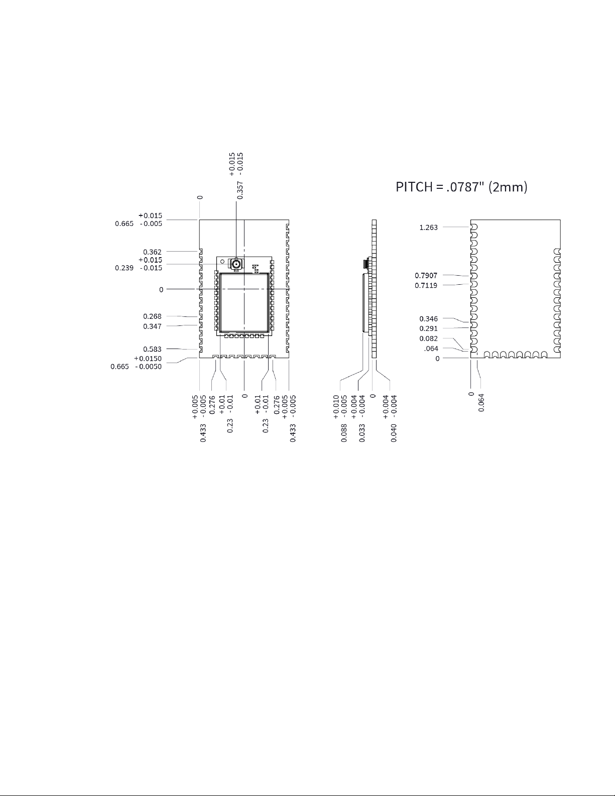
Mechanical drawings
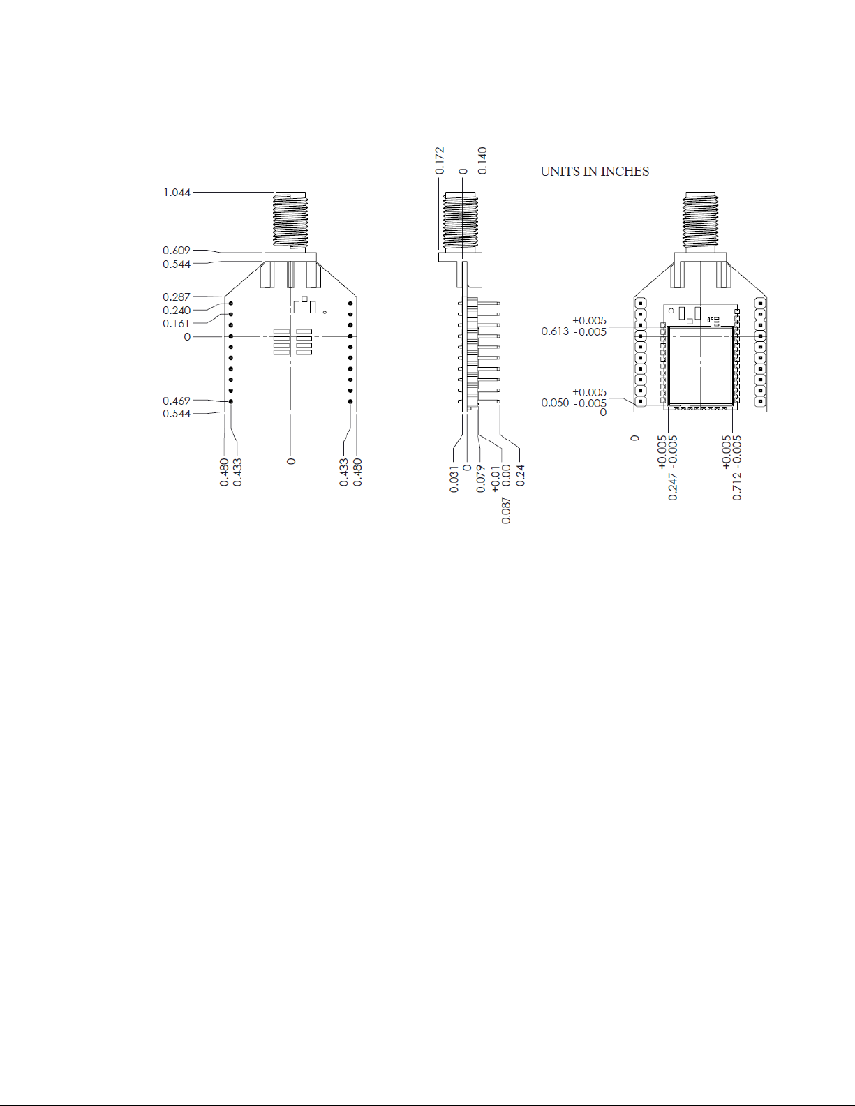
The following mechanical drawings of the XBee 3 RF Modules show all dimensions in inches.
XBee 3 surface-mount antennas 17
XBee 3 micro antennas 19
XBee 3 through-hole antennas 21
Digi XBee® 3 RF Module Hardware Reference Manual
16
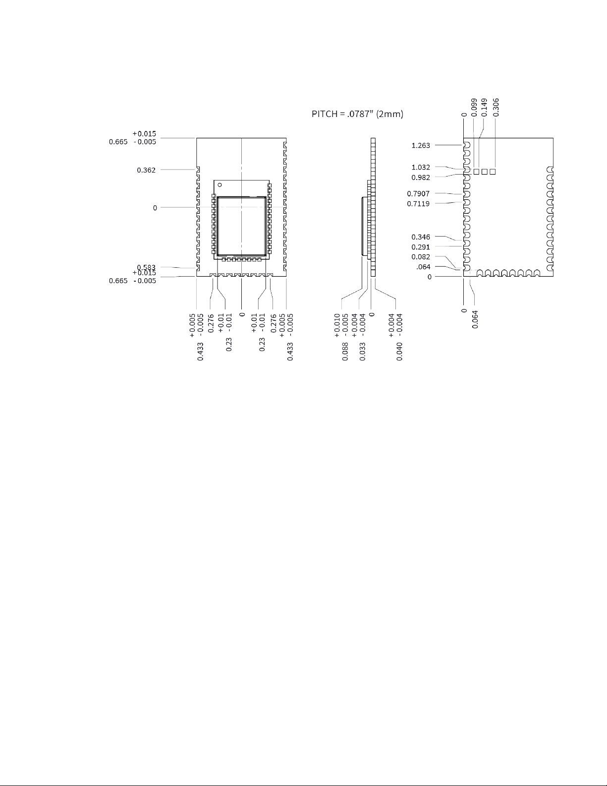
Mechanical drawings XBee 3 surface-mount antennas
XBee 3 surface-mount antennas
The following mechanical drawings are for the XBee 3 surface-mount antennas.
XBee 3 surface-mount - U.FL/RF pad antenna
Digi XBee® 3 RF Module Hardware Reference Manual
17
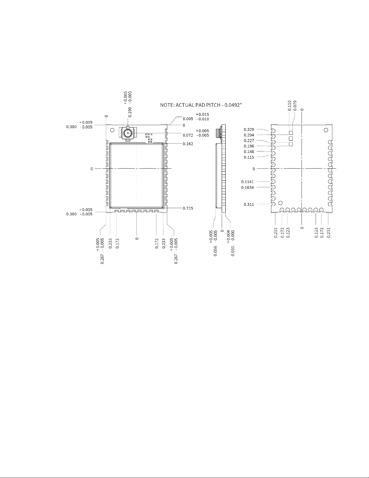
Mechanical drawings XBee 3 surface-mount antennas
XBee 3 surface-mount - embedded antenna
Digi XBee® 3 RF Module Hardware Reference Manual
18
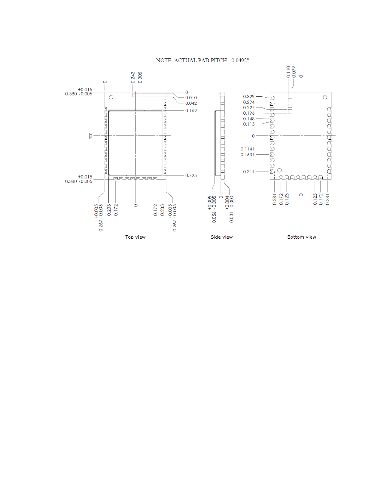
Mechanical drawings XBee 3 micro antennas
XBee 3 micro antennas
The following mechanical drawings are for the XBee 3 micro antennas.
XBee 3 micro (U.FL/RF Pad)
Digi XBee® 3 RF Module Hardware Reference Manual
19
Mechanical drawings XBee 3 micro antennas
XBee 3 micro (chip antenna)
Digi XBee® 3 RF Module Hardware Reference Manual
20
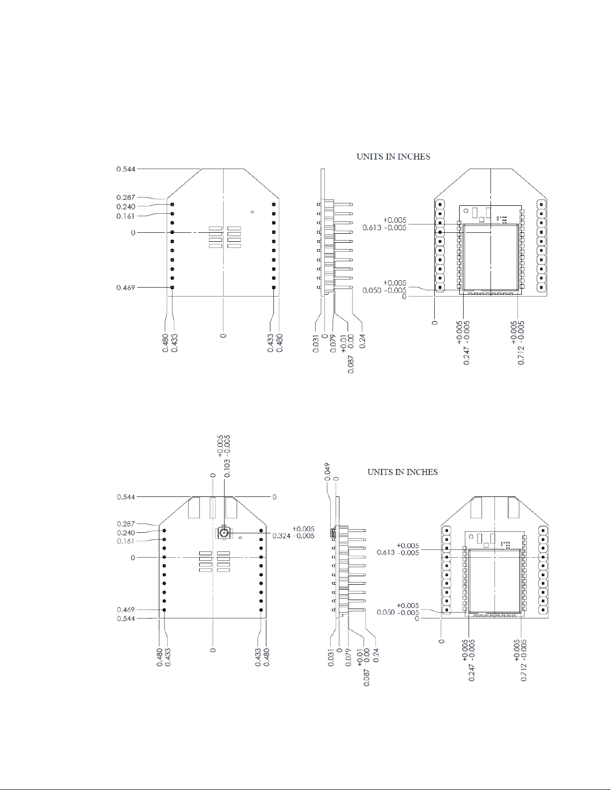
Mechanical drawings XBee 3 through-hole antennas
XBee 3 through-hole antennas
The following mechanical drawings are for the XBee 3 through-hole antennas.
XBee 3 through-hole - PCB antenna
XBee 3 through-hole - U.FL antenna
Digi XBee® 3 RF Module Hardware Reference Manual
21
Mechanical drawings XBee 3 through-hole antennas
XBee 3 through-hole - RPSMA antenna
Digi XBee® 3 RF Module Hardware Reference Manual
22

Pin signals
Pin signals for the XBee 3 surface-mount module 24
Pin signals for the XBee 3 micro module 27
Pin signals for the XBee 3 through-hole module 30
Recommended pin connections 31
Digi XBee® 3 RF Module Hardware Reference Manual
23
Pin signals Pin signals for the XBee 3 surface-mount module
Pin signals for the XBee 3 surface-mount module
The following drawing shows the surface-mount (SMT) pin locations.
The following table shows the pin signals and their descriptions for the surface-mount device.
Pin# Name Direction Default state Description
1 GND - - Ground.
2 VCC - - Power supply.
3 DOUT /DIO13 Both Output UART data out /GPIO.
4 DIN / CONFIG
/DIO14
5 DIO12 Both GPIO.
6 RESET Input Device reset.
7 RSSI PWM/DIO10 Both Output RX signal strength
8 PWM1/DIO11/I2C
SDA
9 [reserved] - Disabled Do not connect.
Both Input UART data in /GPIO.
Indicator /GPIO.
Both Disabled Pulse width
modulator/GPIO/I2C
SDA.
Digi XBee® 3 RF Module Hardware Reference Manual
24

Pin signals Pin signals for the XBee 3 surface-mount module
Pin# Name Direction Default state Description
10 DTR/SLEEP_RQ
/DIO8
11 GND - - Ground.
12 SPI_ATTN/
BOOTMODE
/DIO19
13 GND - - Ground.
14 SPI_CLK /DIO18 Input Input Serial peripheral
15 SPI_SSEL/DIO17 Input Input Serial peripheral
16 SPI_MOSI/DIO16 Input Input Serial peripheral
17 SPI_MISO/DIO15 Output Output Serial peripheral
18 [reserved] - Disabled Do not connect.
Both Input Pin sleep control
Line/GPIO.
Serial peripheral
Output Output
interface attention .
Do not tie low on reset.
interface clock/GPIO.
interface not
select/GPIO.
interface data in/GPIO.
interface data
out/GPIO.
19 [reserved] - Disabled
20 [reserved] - Disabled
21 [reserved] - Disabled
22 GND - - Ground.
23 [reserved] - Disabled Do not connect.
24 DIO4 Both Disabled GPIO.
25 CTS/DIO7 Both Output Clear to send flow
26 ON/SLEEP/DIO9 Both Output Device status
27 [reserved] - Disabled
Do not connect.
Do not connect.
Do not connect.
control/GPIO.
indicator/GPIO
Do not connect or
connect to Ground.
Digi XBee® 3 RF Module Hardware Reference Manual
25

Pin signals Pin signals for the XBee 3 surface-mount module
Pin# Name Direction Default state Description
28 ASSOCIATE/DIO5 Both Output Associate
Indicator/GPIO.
29 RTS/DIO6 Both Input Request to send flow
control /GPIO.
30 AD3/DIO3 Both Disabled Analog input/GPIO.
31 AD2/DIO2 Both Disabled
32 AD1/DIO1/I2C
SCL
33 AD0 /DIO0 Both Input Analog input / GPIO /
34 [reserved] - Disabled Do not connect.
35 GND - - Ground.
36 RF Both - RF I/O for RF pad
37 [reserved] - Disabled Do not connect.
Signal direction is specified with respect to the device.
This is a complete list of functionalities. See the applicable software manual for available
functionalities.
Note There are a possible three RF test points located on the bottom of the device. Do not connect
these test points. For more information, see Recommended footprint.
See Design notes for details on pin connections.
Both Disabled
Analog input/GPIO
Analog input/GPIO/I2C
SCL.
Commissioning button.
variant.
Digi XBee® 3 RF Module Hardware Reference Manual
26

Pin signals Pin signals for the XBee 3 micro module
Pin signals for the XBee 3 micro module
The following drawing shows the micro pin locations.
The following table shows the pin signals and their descriptions for the XBee 3 Micro device.
Default
Pin# Name Direction
1 GND - - Ground.
2 VCC - - Power supply.
3 DOUT /DIO13 Both Output UART data out
4 DIN / CONFIG /DIO14 Both Input UART data in /GPIO.
5 DIO12 Both GPIO.
6 RESET Input Device reset.
7 RSSI PWM/DIO10 Both Output RX signal strength
8 PWM1/DIO11/I2C SDA Both Disabled Pulse width
9 DTR/SLEEP_RQ /DIO8 Both Input Pin sleep control
state Description
/GPIO.
Indicator /GPIO.
modulator/GPIO/I2C
SDA.
Line/GPIO.
Digi XBee® 3 RF Module Hardware Reference Manual
27

Pin signals Pin signals for the XBee 3 micro module
Default
Pin# Name Direction
10 GND - - Ground.
11 SPI_ATTN/ BOOTMODE/DIO19 Output Output
12 GND - - Ground.
13 SPI_CLK /DIO18 Input Input Serial peripheral
14 SPI_SSEL/DIO17 Input Input Serial peripheral
15 SPI_MOSI/DIO16 Input Input Serial peripheral
state Description
Serial peripheral
interface attention
Do not tie low on
reset.
interface
clock/GPIO.
interface not
select/GPIO.
interface data
in/GPIO.
16 SPI_MISO/DIO15 Output Output Serial peripheral
interface data
out/GPIO.
17 [reserved] - Disabled Do not connect.
18 [reserved] - Disabled
19 [reserved] - Disabled
20 [reserved] - Disabled
21 GND - - Ground.
22 [reserved] - Disabled Do not connect.
23 DIO4 Both Disabled GPIO.
24 CTS/DIO7 Both Output Clear to send flow
25 ON/SLEEP/DIO9 Both Output Device status
26 ASSOCIATE/DIO5 Both Output Associate
27 RTS/DIO6 Both Input Request to send
Do not connect.
Do not connect.
Do not connect.
control/GPIO.
indicator/GPIO.
Indicator/GPIO.
flow control /GPIO.
28 AD3/DIO3 Both Disabled Analog input/GPIO.
Digi XBee® 3 RF Module Hardware Reference Manual
28

Pin signals Pin signals for the XBee 3 micro module
Default
Pin# Name Direction
state Description
29 AD2/DIO2 Both Disabled
30 AD1/DIO1/I2C SCL Both Disabled
31 AD0 /DIO0 Both Input Analog input / GPIO
32 GND - - Ground.
33 RF Both - RF I/O for RF pad
34 GND - - Ground.
Signal direction is specified with respect to the device.
This is a complete list of functionalities. See the applicable software manual for available
functionalities.
Note There are three RF test points located on the bottom of the device. Do not connect these test
points. For more information, see Recommended footprint.
See Design notes for details on pin connections.
Analog input/GPIO.
Analog
input/GPIO/I2C SCL.
/ Commissioning
button.
variant.
Digi XBee® 3 RF Module Hardware Reference Manual
29

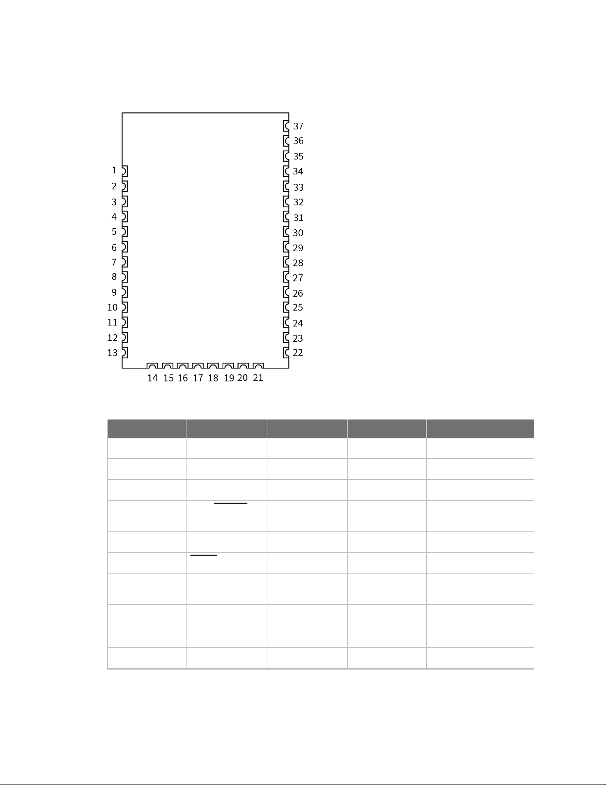
Pin signals Pin signals for the XBee 3 through-hole module
Pin signals for the XBee 3 through-hole module
The following drawing shows the through-hole pin locations.
The following table shows the pin signals and their descriptions for the XBee 3 though-hole device.
Default
Pin# Name Direction
1
VCC - - Power supply.
2
DOUT/DIO13 Both Output UART data
3 DIN/CONFIG/DIO14
4
DIO12/SPI_MISO Both - GPIO/SPI data out.
5 RESET Input
6
RSSI PWM/DIO10 Both Output RX signal Indicator
7
PWM1/DIO11/I2C SDA Both Disabled Pulse width
8
[reserved] - Disabled Do not connect.
9 DTR/SLEEP_RQ/DIO8
Both Intput UART data in/GPIO.
Both Input Pin sleep control
state Description
out/GPIO.
- Device reset.
strength/GPIO.
modulator/GPIO/I2C
SDA.
Line/GPIO.
10
GND - - Ground.
Digi XBee® 3 RF Module Hardware Reference Manual
30

Pin signals Recommended pin connections
Default
Pin# Name Direction
state Description
11
DIO4/SPI_MOSI Both Disabled
12 CTS/DIO7
13 ON/SLEEP/DIO9
14
[reserved] - Disabled Do not connect or
15
ASSOCIATE/DIO5 Both Output Associate
16 RTS/DIO6
17 AD3/DIO3/SPI_SSEL
18
AD2/DIO2/SPI_CLK Both Disabled Analog
19 AD1/DIO1/SPI_ATTN/I2C SCL
Both Output Clear to send flow
Both Output Device status
Both Input Request to send
Both Disabled Analog
Both Disabled Analog
GPIO/Serial
peripheral interface
data in.
control/GPIO.
indicator/GPIO.
connect to Ground.
Indicator/GPIO.
flow control/GPIO.
input/GPIO/SPI not
select.
input/GPIO/SPI
clock.
input/GPIO/SPI
attention/I2C SCL.
20
AD0 /DIO0 Both Input Analog input/GPIO/
Signal direction is specified with respect to the device.
This is a complete list of functionalities. See the applicable software manual for available
functionalities.
See Design notes for details on pin connections.
*
The I2C functionality will be software enabled in a future release.
Recommended pin connections
The only required pin connections for two-way communication are VCC, GND, DOUT and DIN. To
support serial firmware updates and recovery, you must connect VCC, GND, DOUT, DIN, RTS, and DTR.
For applications that need to ensure the lowest sleep current, never leave unconnected inputs
floating. Use internal or external pull-up or pull-down resistors, or set the unused I/O lines to outputs.
Commissioning
button.
Digi XBee® 3 RF Module Hardware Reference Manual
31

Design notes Recommended pin connections
Design notes
XBee 3 modules do not require any external circuitry or specific connections for proper operation.
However, there are some general design guidelines that we recommend to build and troubleshoot a
robust design.
Power supply design 33
Board layout 33
Antenna performance 33
Design notes for PCB antenna and chip antenna devices 34
Design notes for RF pad devices 37
Copper keepout for test points 39
Digi XBee® 3 RF Module Hardware Reference Manual
32

Design notes Power supply design
Power supply design
A poor power supply can lead to poor device performance, especially if you do not keep the supply
voltage within tolerance or if it is excessively noisy. To help reduce noise, place a 1.0 µF and 8.2 pF
capacitor as near as possible to the VCC connection on the XBee 3 (pad 2 for micro and surfacemount, and pin 1 for through-hole). Adding a 10 µF decoupling capacitor is also recommended. If you
are using a switching regulator for the power supply, switch the frequencies above 500 kHz. Limit the
power supply ripple to a maximum 50 mV peak to peak. For best results, place the lower capacitance
capacitors closest to the XBee 3 device.
Note XBee 3 parts with an early revision of the microcontroller unit (MCU) may experience an issue
recovering from brownouts under rare conditions. See Brownout issue for details on how to avoid this
issue.
Board layout
We design XBee 3 modules to be self-sufficient and have minimal sensitivity to nearby processors,
crystals or other printed circuit board (PCB) components. Keep power and ground traces thicker than
signal traces and make sure that they are able to comfortably support the maximum current
specifications. There are no other special PCB design considerations to integrate XBee 3 modules,
with the exception of antennas.
Antenna performance
Antenna location is important for optimal performance. The following suggestions help you achieve
optimal antenna performance. Point the antenna up vertically (upright). Antennas radiate and receive
the best signal perpendicular to the direction they point, so a vertical antenna's omnidirectional
radiation pattern is strongest across the horizon.
Position the antennas away from metal objects whenever possible. Metal objects between the
transmitter and receiver can block the radiation path or reduce the transmission distance. Objects
that are often overlooked include:
n Metal poles
n Metal studs
n Structure beams
n Concrete, which is usually reinforced with metal rods
If you place the device inside a metal enclosure, use an external antenna. Common objects that have
metal enclosures include:
n Vehicles
n Elevators
n Ventilation ducts
n Refrigerators
n Microwave ovens
n Batteries
n Tall electrolytic capacitors
Use the following additional guidelines for optimal antenna performance:
Digi XBee® 3 RF Module Hardware Reference Manual
33

Design notes Design notes for PCB antenna and chip antenna devices
n Do not place XBee 3 devices with the chip antenna or the embedded antenna inside a metal
enclosure.
n Do not place any ground planes or metal objects above or below the antenna.
n For the best results, mount the device at the edge of the host PCB. Ensure that the ground,
power, and signal planes are vacant immediately below the antenna section.
Design notes for PCB antenna and chip antenna devices
Position PCB/chip antenna devices so there are no ground planes or metal objects above or below the
antenna. For best results, do not place the device in a metal enclosure, as this may greatly reduce the
range. Place the device at the edge of the PCB on which it is mounted. Make sure the ground, power
and signal planes are vacant immediately below the antenna section.
The following drawings illustrate important recommendations when you are designing with PCB/chip
antenna devices. For optimal performance on the surface-mount device, do not mount the device on
the RF pad footprint described in the next section, because the footprint requires a ground plane
within the PCB antenna keepout area.
Surface-mount embedded antenna keepout area
Digi XBee® 3 RF Module Hardware Reference Manual
34

Design notes Design notes for PCB antenna and chip antenna devices
Notes
1. We recommend non-metal enclosures. For metal enclosures, use an external antenna.
2. Keep metal chassis or mounting structures in the keepout area at least 2.54 cm (1 in) from the
antenna.
3. Maximize the distance between the antenna and metal objects that might be mounted in the
keepout area.
4. These keepout area guidelines do not apply for chip antennas or external RF connectors.
XBee 3 Micro chip antenna keepout area
Digi XBee® 3 RF Module Hardware Reference Manual
35

Design notes Design notes for PCB antenna and chip antenna devices
Notes
1. We recommend non-metal enclosures. For metal enclosures, use an external antenna.
2. Keep metal chassis or mounting structures in the keepout area at least 2.54 cm (1 in) from the
antenna.
3. Maximize the distance between the antenna and metal objects that might be mounted in the
keepout area.
4. Neither a copper pour nor a copper keepout is necessary under the shield area for proper
antenna functionality. It is still necessary to follow the recommendations in Recommended
footprint for the PCB layout.
5. These keepout area guidelines do not apply for surface-mount embedded antennas or external
RFconnectors.
Through-hole embedded antenna keepout area
Notes
1. We recommend non-metal enclosures. For metal enclosures, use an external antenna.
2. Keep metal chassis or mounting structures in the keepout area at least 2.54 cm (1 in) from the
antenna.
Digi XBee® 3 RF Module Hardware Reference Manual
36

Design notes Design notes for RF pad devices
3. Maximize the distance between the antenna and metal objects that might be mounted in the
keepout area.
4. These keepout area guidelines do not apply for external RF connectors.
Design notes for RF pad devices
The RF pad is a soldered antenna connection. The RF signal travels from the RF pad connection (pad
33 on micro modules and pad 36 on surface-mount modules) on the device to the antenna through an
RF trace transmission line on the PCB. Any additional components between the device and antenna
violates modular certification. The controlled impedance for the RF trace is 50 Ω.
We recommend using a microstrip trace, although you can also use a coplanar waveguide if you need
more isolation. A microstrip generally requires less area on the PCB than a coplanar waveguide. We do
not recommend using a stripline because sending the signal to different PCB layers can introduce
matching and performance problems.
Following good design practices is essential when implementing the RF trace on a PCB. Consider the
following points:
n Minimize the length of the trace by placing the RPSMA jack close to the device.
n Connect all of the grounds on the jack and the device to the ground planes directly or through
closely placed vias.
n Space any ground fill on the top layer at least twice the distance d, for Micro modules at least
0.028" and for surface mount modules at least 0.050".
Additional considerations:
n The top two layers of the PCB have a controlled thickness dielectric material in between.
n The second layer has a ground plane which runs underneath the entire RF pad area. This
ground plane is a distance d, the thickness of the dielectric, below the top layer.
n The RF trace width determines the impedance of the transmission line with relation to the
ground plane. Many online tools can estimate this value, although you should consult the PCB
manufacturer for the exact width.
Implementing these design suggestions helps ensure that the RF pad device performs to its
specifications.
The following figures show a layout example of a host PCB that connects an RF pad device to a right
angle, through-hole RPSMA jack.
Digi XBee® 3 RF Module Hardware Reference Manual
37

Design notes Design notes for RF pad devices
Number Description
1
2 RF pad pin.
3 50 Ω microstrip trace.
4 RF connection of RPSMA jack.
This example is on a surface-mount device. The width in this example is approximately 0.045" for a 50
Ω trace, assuming d=0.025”, and that the dielectric has a relative permittivity of 4.4. This trace width
is a good fit with the device footprint's 0.060" pad width.
Note We do not recommend using a trace wider than the pad width, and using a very narrow trace
(under 0.010") can cause unwanted RF loss.
The following illustration shows PCB layer 2 of an example RF layout.
Maintain a distance of at least 2 d between microstrip and ground fill.
Digi XBee® 3 RF Module Hardware Reference Manual
38

Design notes Copper keepout for test points
Number Description
1
2 Put a solid ground plane under RF trace to achieve the desired impedance.
Use multiple vias to help eliminate ground variations.
Copper keepout for test points
The following keepouts are required for all surface-mount or micro-mount devices. These keepouts
are in addition to the other keepouts if using a PCB or chip antenna.
While the underside of the device is mostly coated with solder resist, we recommended the copper
layer directly below the device be left open to avoid unintended contacts. Copper or vias must not
interfere with the three exposed RF test points on the bottom of the device as shown in the following
diagrams. These devices have a ground plane in the middle on the back side for shielding purposes,
which can be affected by copper traces directly below the device.
Digi XBee® 3 RF Module Hardware Reference Manual
39

Design notes Copper keepout for test points
Copper keepout for the XBee 3 surface-mount
Digi XBee® 3 RF Module Hardware Reference Manual
40

Design notes Copper keepout for test points
Copper keepout for the XBee 3 Micro
Digi XBee® 3 RF Module Hardware Reference Manual
41

Regulatory information
United States (FCC) 43
Europe (CE) 53
ISED (Innovation, Science and Economic Development Canada) 55
Australia (RCM)/New Zealand 56
Brazil ANATEL 56
Japan (TELEC) 57
Mexico (IFETEL) 58
South Korea 58
Digi XBee® 3 RF Module Hardware Reference Manual
42

Regulatory information United States (FCC)
United States (FCC)
XBee 3 RF Modules comply with Part 15 of the FCC rules and regulations. Compliance with the labeling
requirements, FCC notices and antenna usage guidelines is required.
To fulfill FCC Certification, the OEM must comply with the following regulations:
1. The system integrator must ensure that the text on the external label provided with this
device is placed on the outside of the final product.
2. RF Modules may only be used with antennas that have been tested and approved for use with
the modules.
OEM labeling requirements
WARNING! As an Original Equipment Manufacturer (OEM) you must ensure that FCC
labeling requirements are met. You must include a clearly visible label on the outside of the
final product enclosure that displays the following content:
Required FCC Label for OEM products containing the XBee 3 RF Module
Contains FCC ID: MCQ-XBEE3
This device complies with Part 15 of the FCC Rules. Operation is subject to the following two
conditions: (1.) this device may not cause harmful interference and (2.) this device must accept any
interference received, including interference that may cause undesired operation.
FCC notices
IMPORTANT: XBee 3 RF Modules have been certified by the FCC for use with other products without
any further certification (as per FCC section 2.1091). Modifications not expressly approved by Digi
could void the user's authority to operate the equipment.
IMPORTANT: OEMs must test final product to comply with unintentional radiators (FCC section 15.107
& 15.109) before declaring compliance of their final product to Part 15 of the FCC Rules.
IMPORTANT: The RF module has been certified for remote and base radio applications. If the module
will be used for portable applications, the device must undergo SAR testing.
This equipment has been tested and found to comply with the limits for a Class B digital device,
pursuant to Part 15 of the FCC Rules. These limits are designed to provide reasonable protection
against harmful interference in a residential installation. This equipment generates, uses and can
radiate radio frequency energy and, if not installed and used in accordance with the instructions, may
cause harmful interference to radio communications. However, there is no guarantee that
interference will not occur in a particular installation.
If this equipment does cause harmful interference to radio or television reception, which can be
determined by turning the equipment off and on, the user is encouraged to try to correct the
interference by one or more of the following measures: Re-orient or relocate the receiving antenna,
Increase the separation between the equipment and receiver, Connect equipment and receiver to
outlets on different circuits, or Consult the dealer or an experienced radio/TV technician for help.
Digi XBee® 3 RF Module Hardware Reference Manual
43

Regulatory information United States (FCC)
FCC-approved antennas (2.4 GHz)
The XBee 3 RF Module can be installed using antennas and cables constructed with non-standard
connectors (RPSMA, RPTNC, etc.) An adapter cable may be necessary to attach the XBee connector to
the antenna connector.
The modules are FCC approved for fixed base station and mobile applications for the channels
indicated in the tables below. If the antenna is mounted at least 20 cm (7.87 in) from nearby persons,
the application is considered a mobile application. Antennas not listed in the table must be tested to
comply with FCC Section 15.203 (Unique Antenna Connectors) and Section 15.247 (Emissions).
The antennas in the tables below have been approved for use with this module. Cable loss is required
when using gain antennas as shown in the tables.
Digi does not carry all of these antenna variants. Contact Digi Sales for available antennas.
1. If using the RF module in a portable application (for example, if the module is used in a hand-
held device and the antenna is less than 20 cm from the human body when the device is in
operation), The integrator is responsible for passing additional Specific Absorption Rate (SAR)
testing based on FCC rules 2.1091 and FCC Guidelines for Human Exposure to Radio Frequency
Electromagnetic Fields, OET Bulletin and Supplement C. The testing results will be submitted
to the FCC for approval prior to selling the integrated unit. The required SAR testing measures
emissions from the module and how they affect the person.
Digi XBee® 3 RF Module Hardware Reference Manual
44

Digi XBee® 3 RF Module Hardware Reference Manual 45
Regulatory information United States (FCC)
XBee 3 RF module
The following table shows the antennas approved for use with the XBee 3 RF module.
All antenna part numbers followed by an asterisk (*) are not available from Digi. Consult with an antenna manufacturer for an equivalent option.
Required antenna cable loss (dB)
802.15.4 Based
Type
Partnumber
Integral antennas
29000313 Integral PCB antenna (surface-
29000710 Chip antenna (micro only) 0.0 Fixed/Mobile 20 cm N/A N/A
29000294 Integral PCB antenna (through-hole
Dipole antennas
31000019-01 Integral Dipole (USB Adapter Only) 0.87 Portable N/A N/A N/A
A24-HASM-450 Dipole (Half-wave articulated RPSMA
A24-HABSM* Dipole (Articulated RPSMA) 2.1 Fixed 20 cm N/A N/A
29000095 Dipole (Half-wave articulated RPSMA
A24-HABUF-P5I Dipole (Half-wave articulated
(description)
mount only)
only)
- 4.5”)
- 4.5”)
bulkhead mount U.FL. w/ 5” pigtail)
Gain
(dBi) Application* Min. separation
0.0 Fixed/Mobile 20 cm N/A N/A
-0.5
dBi
2.1 Fixed 20 cm N/A N/A
2.1 Fixed/Mobile 20 cm N/A N/A
2.1 Fixed/Mobile 20 cm N/A N/A
Fixed/Mobile 20 cm N/A N/A
Protocols (Ex:
Zigbee)
Bluetooth low energy
technology (when
available)
A24-HASM-525 Dipole (Half-wave articulated RPSMA
- 5.25")
2.1 Fixed 20 cm N/A N/A

Digi XBee® 3 RF Module Hardware Reference Manual 46
Required antenna cable loss (dB)
Regulatory information United States (FCC)
Type
Partnumber
Omni-directional (Collinear Dipole Array)antennas
A24-F2NF Omni-directional (Fiberglass base
A24-F3NF Omni-directional (Fiberglass base
A24-F5NF Omni-directional (Fiberglass base
A24-F8NF Omni-directional (Fiberglass base
A24-F9NF Omni-directional (Fiberglass base
A24-F10NF Omni-directional (Fiberglass base
A24-F12NF Omni-directional (Fiberglass base
A24-W7NF Omni-directional (Fiberglass base
(description)
station)
station)
station)
station)
station)
station)
station)
station)
802.15.4 Based
Gain
(dBi) Application* Min. separation
2.1 Fixed/Mobile 20 cm N/A N/A
3.0 Fixed/Mobile 20 cm N/A N/A
5.0 Fixed 20 cm N/A N/A
8.0 Fixed 2 m N/A N/A
9.5 Fixed 2 m N/A N/A
10.0 Fixed 2 m N/A N/A
12.0 Fixed 2 m N/A N/A
7.2 Fixed 2 m N/A N/A
Protocols (Ex:
Zigbee)
Bluetooth low energy
technology (when
available)
A24-M7NF Omni-directional (Mag-mount base
station)
A24-F15NF Omni-directional (Fiberglass base
station)
Panel antennas
A24-P8SF Flat Panel 8.5 Fixed 2 m N/A N/A
7.2 Fixed 2 m N/A N/A
15.0 Fixed 2 m N/A N/A

Digi XBee® 3 RF Module Hardware Reference Manual 47
Regulatory information United States (FCC)
Required antenna cable loss (dB)
Partnumber
Type
(description)
Gain
(dBi) Application* Min. separation
802.15.4 Based
Protocols (Ex:
Zigbee)
Bluetooth low energy
technology (when
available)
A24-P8NF Flat Panel 8.5 Fixed 2 m N/A N/A
A24-P13NF Flat Panel 13.0 Fixed 2 m N/A N/A
A24-P14NF Flat Panel 14.0 Fixed 2 m N/A N/A
A24-P15NF Flat Panel 15.0 Fixed 2 m N/A N/A
A24-P16NF Flat Panel 16.0 Fixed 2 m N/A N/A
A24-P19NF Flat Panel 19.0 Fixed 2 m
N/A
N/A
Yagi antennas
A24-Y6NF Yagi (6-element) 8.8 Fixed 2 m N/A N/A
A24-Y7NF Yagi (7-element) 9.0 Fixed 2 m N/A N/A
A24-Y9NF Yagi (9-element) 10.0 Fixed 2 m N/A N/A
A24-Y10NF Yagi (10-element) 11.0 Fixed 2 m N/A N/A
A24-Y12NF Yagi (12-element) 12.0 Fixed 2 m N/A N/A
A24-Y13NF Yagi (13-element) 12.0 Fixed 2 m N/A N/A
A24-Y15NF Yagi (15-element) 12.5 Fixed 2 m N/A N/A
A24-Y16NF Yagi (16-element) 13.5 Fixed 2 m N/A N/A
A24-Y16RM Yagi (16-element, RPSMA connector) 13.5 Fixed 2 m N/A N/A
A24-Y18NF Yagi (18-element) 15.0 Fixed 2 m N/A N/A
Patch antenna
Taoglas
2.4 GHz band antenna 4 Fixed 20 cm N/A N/A
FXP74.07.0100A

Digi XBee® 3 RF Module Hardware Reference Manual 48
Regulatory information United States (FCC)
XBee3-PRO RF module
The following table shows the antennas approved for use with the XBee3-PRO RF Module.
All antenna part numbers followed by an asterisk (*) are not available from Digi. Consult with an antenna manufacturer for an equivalent option.
Required antenna cable loss (dB)
Partnumber Type (description)
Internal antennas
29000313 Integral PCB
antenna (surface
mount only)
29000710 Chip antenna
(micro only)
29000294 Integral PCB
antenna (throughhole only)
Dipole antennas
A24-HASM-450 Dipole (Half-wave
articulated RPSMA -
4.5”)
A24-HABSM* Dipole (Articulated
RPSMA)
29000095 Dipole (Half-wave
articulated RPSMA -
4.5”)
802.15.4 Based
Protocols (Ex:
Gain (dBi)
0.0 Fixed/Mobile 20 cm N/A N/A
0.0 Fixed/Mobile 20 cm N/A N/A
-0.5 dBi Fixed/Mobile 20 cm N/A N/A
2.1 Fixed 20 cm N/A N/A
2.1 Fixed 20 cm N/A N/A
2.1 Fixed/Mobile 20 cm N/A N/A
Application* Min separation
Zigbee)
Bluetooth low
energy technology
(when available)

Digi XBee® 3 RF Module Hardware Reference Manual 49
Required antenna cable loss (dB)
Regulatory information United States (FCC)
Partnumber Type (description)
A24-HABUF-P5I Dipole (Half-wave
articulated
bulkhead mount
U.FL. w/ 5” pigtail)
A24-HASM-525 Dipole (Half-wave
articulated RPSMA -
5.25")
31000019-01 Integral Dipole
(USB Adapter Only)
Omni-directional (Collinear Dipole Array) antennas
A24-F2NF Omni-directional
(Fiberglass base
station)
A24-F3NF Omni-directional
(Fiberglass base
station)
A24-F5NF Omni-directional
(Fiberglass base
station)
Gain (dBi)
2.1 Fixed/Mobile 20 cm N/A N/A
2.1 Fixed 20 cm N/A N/A
0.87 Fixed only 20 cm N/A N/A
2.1 Fixed/Mobile 20 cm N/A N/A
3.0 Fixed/Mobile 20 cm N/A N/A
5.0 Fixed 20 cm N/A N/A
Application* Min separation
802.15.4 Based
Protocols (Ex:
Zigbee)
Bluetooth low
energy technology
(when available)
A24-F8NF Omni-directional
(Fiberglass base
station)
A24-F9NF Omni-directional
(Fiberglass base
station)
8.0 Fixed 2 m N/A N/A
9.5 Fixed 2 m N/A N/A

Digi XBee® 3 RF Module Hardware Reference Manual 50
Regulatory information United States (FCC)
Required antenna cable loss (dB)
Partnumber Type (description)
A24-F10NF Omni-directional
802.15.4 Based
Protocols (Ex:
Gain (dBi)
Application* Min separation
Zigbee)
10 Fixed 2 m N/A N/A
Bluetooth low
energy technology
(when available)
(Fiberglass base
station)
A24-F12NF Omni-directional
12 Fixed 2 m N/A N/A
(Fiberglass base
station)
A24-W7NF Omni-directional
7.2 Fixed 2 m N/A N/A
(Fiberglass base
station)
A24-M7NF Omni-directional
7.2 Fixed 2 m N/A N/A
(Mag-mount base
station)
A24-F15NF Omni-directional
15.0 Fixed 2 m N/A 2.0
(Fiberglass base
station)
Panel antennas
A24-P8SF Flat Panel 8.5 Fixed 2 m N/A N/A
A24-P8NF Flat Panel 8.5 Fixed 2 m N/A N/A
A24-P13NF Flat Panel 13.0 Fixed 2 m N/A N/A
A24-P14NF Flat Panel 14.0 Fixed 2 m N/A 1.0
A24-P15NF Flat Panel 15.0 Fixed 2 m N/A 2.0
A24-P16NF Flat Panel 16.0 Fixed 2 m N/A 3.0
A24-P19NF Flat Panel 19.0 Fixed 2 m 3.0 6.0

Digi XBee® 3 RF Module Hardware Reference Manual 51
Regulatory information United States (FCC)
Required antenna cable loss (dB)
Partnumber Type (description)
Gain (dBi)
Application* Min separation
802.15.4 Based
Protocols (Ex:
Zigbee)
Bluetooth low
energy technology
(when available)
Yagi antennas
A24-Y6NF Yagi (6-element) 8.8 Fixed 2 m N/A N/A
A24-Y7NF Yagi (7-element) 9.0 Fixed 2 m N/A N/A
A24-Y9NF Yagi (9-element) 10.0 Fixed 2 m N/A N/A
A24-Y10NF Yagi (10-element) 11.0 Fixed 2 m N/A N/A
A24-Y12NF Yagi (12-element) 12.0 Fixed 2 m N/A N/A
A24-Y13NF Yagi (13-element) 12.0 Fixed 2 m N/A N/A
A24-Y15NF Yagi (15-element) 12.5 Fixed 2 m N/A N/A
A24-Y16NF Yagi (16-element) 13.5 Fixed 2 m N/A 0.5
A24-Y16RM Yagi (16-element,
13.5 Fixed 2 m N/A 0.5
RPSMA connector)
A24-Y18NF Yagi (18-element) 15.0 Fixed 2 m N/A 2.0
Patch antenna
Taoglas
FXP74.07.0100A
2.4 GHz band
antenna
4 Fixed 20 cm N/A N/A
* If using the RF module in a portable application (for example - if the module is used in a handheld device and the antenna is less than 20 cm from the
human body when the device is in operation): The integrator is responsible for passing additional SAR (Specific Absorption Rate) testing based on FCC
rules 2.1091 and FCC Guidelines for Human Exposure to Radio Frequency Electromagnetic Fields, OET Bulletin and Supplement C. The testing results
will be submitted to the FCC for approval prior to selling the integrated unit. The required SAR testing measures emissions from the module and how
they affect the person.

Regulatory information United States (FCC)
RF exposure
If you are an integrating the XBee 3 into another product, you must include the following Caution
statement in OEMproduct manuals to alert users of FCC RF exposure compliance:
CAUTION! To satisfy FCC RF exposure requirements for mobile transmitting devices, a
separation distance of 20 cm or more should be maintained between the antenna of this
device and persons during device operation. To ensure compliance, operations at closer than
this distance are not recommended. The antenna used for this transmitter must not be colocated in conjunction with any other antenna or transmitter.
XBee 3 USB Adapter
The XBee 3 USB Adapter integrates an XBee 3 RF Module into its hardware. Due to output power
limitations it is exempt from SAR testing. It is approved as a portable application.
FCC publication 996369 related information
In Publication 996369 section D03, the FCC requires information concerning a module to be presented
by OEM manufacturers. This section assists in answering or fulfilling these requirements.
2.1 General
No requirements are associated with this section.
2.2 List of applicable FCC rules
This module conforms to FCC Part 15.247.
2.3 Summarize the specific operational use conditions
Certain approved antennas require attenuation for operation. For the XBee 3, see XBee 3 RF module.
For the Pro XBee 3, see XBee3-PRO RF module.
Host product user guides should include the antenna table if end customers are permitted to select
antennas.
2.4 Limited module procedures
Not applicable.
2.5 Trace antenna designs
While it is possible to build a trace antenna into the host PCB, this requires at least a Class II
permissive change to the FCC grant which includes significant extra testing and cost. If an embedded
trace or chip antenna is desired, simply select the XBee 3 module variant with the preferred antenna.
2.6 RF exposure considerations
For RF exposure considerations see RF exposure and FCC-approved antennas (2.4 GHz).
Host product manufacturers need to provide end-users a copy of the “RF Exposure” section of the
manual: RF exposure.
Digi XBee® 3 RF Module Hardware Reference Manual
52

Regulatory information Europe (CE)
2.7 Antennas
A list of approved antennas is provided for the XBee 3 product. For the XBee 3, see XBee 3 RF module.
For the Pro XBee 3, see XBee3-PRO RF module.
2.8 Label and compliance information
Host product manufacturers need to follow the sticker guidelines outlined in OEM labeling
requirements.
2.9 Information on test modes and additional testing requirements
Contact a Digi sales representative for information on how to configure test modes for the XBee 3
product.
2.10 Additional testing, Part 15 Subpart B disclaimer
All final host products must be tested to be compliant to FCC Part 15 Subpart B standards. While the
XBee3 unit was tested to be compliant to FCC unintentional radiator standards, FCC Part 15 Subpart
B compliance testing is still required for the final host product. This testing is required for all end
products, and XBee 3 Part 15 Subpart B compliance does not affirm the end product’s compliance.
See FCC notices for more details.
Over-voltage detection
Over-Voltage detection sends out a modem status of 0x0D indicating that the voltage supply limit has
been exceeded. The device will still operate but limits the RF power level PL setting to a value of 3
when the operating voltage reaches 3.7 volts or higher to meet regulatory RF power requirements.
While the device is in this mode of operation it will be forced into API mode for the over-voltage
modem status to be sent out the serial port every 15 seconds when API mode is set to 1 or 2.
Europe (CE)
The XBee 3 RF Module has been tested for use in several European countries. For a complete list, refer
to www.digi.com/resources/certifications.
If XBee 3 RF Modules are incorporated into a product, the manufacturer must ensure compliance of
the final product with articles 3.1a and 3.1b of the Radio Equipment Directive. A Declaration of
Conformity must be issued for each of these standards and kept on file as described in the Radio
Equipment Directive.
Furthermore, the manufacturer must maintain a copy of the XBee 3 RF Module user guide
documentation and ensure the final product does not exceed the specified power ratings, antenna
specifications, and/or installation requirements as specified in the user guide.
Maximum power and frequency specifications
For the XBee 3 device:
When using the 802.15.4 RF physical layer:
n Maximum power: 8.61 mW (9.35 dBm) Equivalent Isotropically Radiated Power (EIRP).
n Frequencies: 5 MHz channel spacing, beginning at 2405 MHz and ending at 2480 MHz.
When using the Bluetooth low energy technology RF physical layer:
Digi XBee® 3 RF Module Hardware Reference Manual
53

Regulatory information Europe (CE)
n Maximum power: 9.02 mW (9.55 dBm) Equivalent Isotropically Radiated Power (EIRP).
n Frequencies: 2 MHz channel spacing, beginning at 2402 MHz and ending at 2480 MHz.
OEM labeling requirements
The “CE” marking must be affixed to a visible location on the OEM product. The following figure shows
CE labeling requirements.
The CE mark shall consist of the initials “CE” taking the following form:
n If the CE marking is reduced or enlarged, the proportions given in the above graduated
drawing must be respected.
n The CE marking must have a height of at least 5 mm except where this is not possible on
account of the nature of the apparatus.
n The CE marking must be affixed visibly, legibly, and indelibly.
Important note
Digi customers assume full responsibility for learning and meeting the required guidelines for each
country in their distribution market. Refer to the radio regulatory agency in the desired countries of
operation for more information.
Declarations of conformity
Digi has issued Declarations of Conformity for the XBee 3 RF Modules concerning emissions, EMC, and
safety. For more information, see www.digi.com/resources/certifications.
Antennas
Testing for use of the XBee 3 in the European markets was performed with a 2.1 dBi dipole antenna.
Use of an antenna with a gain of 2.1 dBi or less will ensure compliance with the spectrum
requirements of the RED.
Digi XBee® 3 RF Module Hardware Reference Manual
54

Regulatory information ISED (Innovation, Science and Economic Development Canada)
The following antennas have been tested for use with the XBee 3 RF Module. All antenna part
numbers followed by an asterisk (*) are not available from Digi. Consult with an antenna manufacturer
for an equivalent option.
n Dipole (2.1 dBi, Omni-directional, Articulated RPSMA, Digi part number A24-HABSM)
n PCB antenna (surface mount boards only) (0.0 dBi)
n Chip antenna (micro form factor only) (0.0 dBi)
n PCB antenna (through-hole boards only) (-0.5 dBi)
n Integral Dipole (USB Adapter only) (0.87 dBi)
ISED (Innovation, Science and Economic Development Canada)
Labeling requirements
Labeling requirements for Industry Canada are similar to those of the FCC. A clearly visible label on
the outside of the final product enclosure must display the following text.
For XBee 3
Contains Model XBEE3, IC: 1846A-XBEE3
The integrator is responsible for its product to comply with IC ICES-003 & FCC Part 15, Sub. B Unintentional Radiators. ICES-003 is the same as FCC Part 15 Sub. B and Industry Canada accepts
FCC test report or CISPR 22 test report for compliance with ICES-003.
This device complies with Industry Canada licence-exempt RSS standard(s). Operation is subject to
the following two conditions: (1) this device may not cause interference, and (2) this device must
accept any interference, including interference that may cause undesired operation of the device.
Le présent appareil est conforme aux CNR d'Industrie Canada applicables aux appareils radio exempts
de licence. L'exploitation est autorisée aux deux conditions suivantes: (1) l'appareil ne doit pas
produire de brouillage, et (2) l'utilisateur de l'appareil doit accepter tout brouillage radioélectrique
subi, même si le brouillage est susceptible d'en compromettre le fonctionnement.
RF Exposure
CAUTION! This equipment is approved for mobile and base station transmitting devices only.
Antenna(s) used for this transmitter must be installed to provide a separation distance of at
least 20 cm from all persons and must not be co-located or operating in conjunction with any
other antenna or transmitter.
ATTENTION! Cet équipement est approuvé pour la mobile et la station base dispositifs
d'émission seulement. Antenne(s) utilisé pour cet émetteur doit être installé pour fournir
une distance de séparation d'au moins 20 cm à partir de toutes les personnes et ne doit
pas être situé ou fonctionner en conjonction avec tout autre antenne ou émetteur.
XBee 3 USB Adapter
The XBee 3 USB Adapter integrates an XBee 3 RF Module into its hardware. Special SAR testing was
undertaken for the XBee 3 USB Adapter product to ensure it met IC standards. It is approved as a
Digi XBee® 3 RF Module Hardware Reference Manual
55

Regulatory information Australia (RCM)/New Zealand
portable application.
Transmitters with Detachable Antennas
This radio transmitter (IC: 1846A-XBEE3) has been approved by Industry Canada to operate with the
antenna types listed in FCC-approved antennas (2.4 GHz) with the maximum permissible gain and
required antenna impedance for each antenna type indicated. Antenna types not included in this list,
having a gain greater than the maximum gain indicated for that type, are strictly prohibited for use
with this device.
Le présent émetteur radio (IC: 1846A-XBEE3) a été approuvé par Industrie Canada pour fonctionner
avec les types d'antenne énumérés ci-dessous et ayant un gain admissible maximal et l'impédance
requise pour chaque type d'antenne. Les types d'antenne non inclus dans cette liste, ou dont le gain
est supérieur au gain maximal indiqué, sont strictement interdits pour l'exploitation de l'émetteur.
Detachable Antenna
Under Industry Canada regulations, this radio transmitter may operate using only an antenna of a
type and maximum (or lesser) gain approved for the transmitter by Industry Canada. To reduce
potential radio interference to other users, the antenna type and its gain should be so chosen that the
equivalent isotropically radiated power (EIRP) is not more than that necessary for successful
communication.
Conformément à la réglementation d'Industrie Canada, le présent émetteur radio peutfonctionner
avec une antenne d'un type et d'un gain maximal (ou inférieur) approuvépour l'émetteur par Industrie
Canada. Dans le but de réduire les risques de brouillageradioélectrique à l'intention des autres
utilisateurs, il faut choisir le type d'antenne etson gain de sorte que la puissance isotrope rayonnée
équivalente (p.i.r.e.) ne dépassepas l'intensité nécessaire àl'établissement d'une communication
satisfaisante.
Australia (RCM)/New Zealand
XBee 3 and XBee 3-PROmodules comply with requirements to be used in end products in Australia
and New Zealand. All products with EMC and radio communications must have registered RCM and RNZ marks. Registration to use the compliance mark will only be accepted from Australia or New
Zealand manufacturers or importers, or their agents.
In order to have an RCM or R-NZ mark on an end product, a company must comply with a or b below.
a. have a company presence in Australia or New Zealand.
b. have a company/distributor/agent in Australia or New Zealand that will sponsor the importing
of the end product.
Contact Digi for questions related to locating a contact in Australia and New Zealand.
Brazil ANATEL
The XBee 3 ZigBee, DigiMesh and 802.15.4 radio modules comply with the requirements of ANATEL to
be used in Brazil. The customer's product is subject to testing for conformity to the same Brazilian
standards.
Modelo: XBee 3
Atendimento à Regulamentação Anatel
Digi XBee® 3 RF Module Hardware Reference Manual
56

Regulatory information Japan (TELEC)
Este equipamento não tem direito à proteção contra interferência prejudicial e não pode causar
interferência em sistemas devidamente autorizados.
Este produto está homologado pela ANATEL, de acordo com os procedimentos regulamentados pela
Resolução 242/2000, e atende aos requisitos técnicos aplicados.
Para maiores informações, consulte o site da ANATEL www.anatel.gov.br.
Japan (TELEC)
The XBee 3 (not XBee 3-PRO) complies with Japan MIC Article 2 Paragraph 1, Item 19.
The customer product is subject to testing for conformity to the same Japanese standard.
Digi XBee® 3 RF Module Hardware Reference Manual
57

Regulatory information Mexico (IFETEL)
Mexico (IFETEL)
Manufacturer: Digi International
Country: USA
Brand: Digi
Model: XBEE3
Tariff Code (HS): 8517-62-15
IFETEL (IFT) number RCPDIXB19-1820 applies to these XBee3 radios:
XB3-24ACM XB3-24ACM-J XB3-24ARM XB3-24ARM-J
XB3-24AUM XB3-24AUM-J XB3-24DMCM XB3-24DMCM-J
XB3-24DMRM XB3-24DMRM-J XB3-24DMUM XB3-24DMUM-J
XB3-24Z8CM XB3-24Z8CM-J XB3-24Z8PS XB3-24Z8PS-J
XB3-24Z8PT XB3-24Z8PT-J XB3-24Z8RM XB3-24Z8RM-J
XB3-24Z8RS XB3-24Z8RS-J XB3-24Z8ST XB3-24Z8ST-J
XB3-24Z8UM XB3-24Z8UM-J XB3-24Z8US XB3-24Z8US-J
XB3-24Z8UT XB3-24Z8UT-J
OEM labeling requirements
The IFETEL number for the XBee3 product must be listed either on the end product, on the packaging,
in the manual, or in the software with the following phrase:
“Este equipo contiene el módulo XBee3 con Número IFETEL: RCPDIXB19-1820”
or
“Este equipo contiene el módulo XBee3 con IFT #: RCPDIXB19-1820”
The following paragraph must also be present in the User Manual for the end product:
“La operación de este equipo está sujeta a las siguientes dos condiciones: (1) es posible que
este equipo o dispositivo no cause interferencia perjudicial y (2) este equipo o dispositivo debe
aceptar cualquier interferencia, incluyendo la que pueda causar su operación no deseada.”
South Korea
The XBee 3 (not XBee 3-PRO) complies with South Korea's Korea Communications Commission (KCC)
Clause 2, Article 58-2 of Radio Waves Act.
The customer's product is subject to testing for conformity to the same South Korea standards.
WARNING! The Original Equipment Manufacturer (OEM) must ensure that Mexico IFT
labeling requirements are met.
Digi XBee® 3 RF Module Hardware Reference Manual
58

Regulatory information South Korea
Digi XBee® 3 RF Module Hardware Reference Manual
59

XBIB-C development boards
This section describes the XBIB-C development boards and how to interact with them.
XBIB-C Micro Mount reference 61
XBIB-C SMT reference 63
XBIB-CU TH reference 65
XBIB-C-GPS reference 67
Interface with the XBIB-C-GPS module 69
Attach the XBee 3 RF Module 70
Digi XBee® 3 RF Module Hardware Reference Manual
60

XBIB-C development boards XBIB-C Micro Mount reference
XBIB-C Micro Mount reference
This picture shows the XBee-C Micro Mount development board and the table that follows explains the
callouts in the picture.
Note This board is sold separately.
Digi XBee® 3 RF Module Hardware Reference Manual
61

XBIB-C development boards XBIB-C Micro Mount reference
Number Item Description
1 Secondary USB
(USB MICRO B)
2 Current
Measure
3 Battery
Connector
4 USB-C
Connector
5 LED indicator Red: UART DOUT (modem sending serial/UART data to host)
6 User Buttons Comm DIO0 Button connects the Commissioning/DIO0 pin on the XBee
Secondary USB Connector for possible future use. Not used.
Large switch controls whether current measure mode is active or
inactive. When inactive, current can freely flow to the VCC pin of the
XBee. When active, the VCC pin of the XBee is disconnected from the 3.3
V line on the development board. This allows current measurement to
be conducted by attaching a current meter across the jumper P10.
If desired, you can attach a battery to provide power to the
development board. The voltage can range from 2 V to 5 V. The positive
terminal is on the left.
Connects to your computer. This is connected to a USB to UART
conversion chip that has the five UART lines passed to the XBee device.
The UART Dip Switch can be used to disconnect these UART lines from
the XBee.
Green: UART DIN (modem receiving serial/UART data from host)
White: ON/SLP/DIO9
Blue: Connection Status/DIO5
Yellow: RSSI/PWM0/DIO10
Connector through to a 10 Ω resistor to GND when pressed.
RESET Button Connects to the RESET pin on the XBee Connector to GND
when pressed.
7 Breakout
Connector
8 UART Dip
Switch
9 Grove
Connector
10 Temp/Humidity
Sensor
11 XBee Socket This is the socket for the XBee (Micro form factor).
This 40-pin connector can be used to connect to various XBee pins as
shown on the silkscreen on the bottom of the board.
This dip switch allows the user to disconnect any of the primary UART
lines on the XBee from the USB to UART conversion chip. This allows for
testing on the primary UART lines without the USB to UART conversion
chip interfering. Push Dip switches to the right to disconnect the USB to
UART conversion chip from the XBee.
This connector can be used to attach I2C enabled devices to the
development board. Note that I2C needs to be available on the XBee in
the board to use this functionality.
Pin 1: I2C_CLK/XBee DIO1
Pin2: I2C_SDA/XBee DIO11
Pin3: VCC
Pin4: GND
This as a Texas Instruments HDC1080 temperature and humidity
sensor. This part is accessible through I2C. Be sure that the XBee that is
inserted into the development board has I2C if access to this sensor is
desired.
Digi XBee® 3 RF Module Hardware Reference Manual
62

XBIB-C development boards XBIB-C SMT reference
XBIB-C SMT reference
This picture shows the XBee-C SMT development board and the table that follows explains the
callouts in the picture.
Note This board is sold separately.
Digi XBee® 3 RF Module Hardware Reference Manual
63

XBIB-C development boards XBIB-C SMT reference
Number Item Description
1 Secondary USB
(USB MICRO B)
2 Current
Measure
3 Battery
Connector
4 USB-C
Connector
5 LED indicator Red: UART DOUT (modem sending serial/UART data to host)
6 User Buttons Comm DIO0 Button connects the Commissioning/DIO0 pin on the XBee
Secondary USB Connector for possible future use. Not used.
Large switch controls whether current measure mode is active or
inactive. When inactive, current can freely flow to the VCC pin of the
XBee. When active, the VCC pin of the XBee is disconnected from the 3.3
V line on the dev board. This allows current measurement to be
conducted by attaching a current meter across the jumper P10.
If desired, you can attach a battery to provide power to the
development board. The voltage can range from 2 V to 5 V. The positive
terminal is on the left.
Connects to your computer. This is connected to a USB to UART
conversion chip that has the five UART lines passed to the XBee. The
UART Dip Switch can be used to disconnect these UART lines from the
XBee.
Green: UART DIN (modem receiving serial/UART data from host)
White: ON/SLP/DIO9
Blue: Connection Status/DIO5
Yellow: RSSI/PWM0/DIO10
Connector through to a 10 Ω resistor to GND when pressed.
RESET Button Connects to the RESET pin on the XBee Connector to GND
when pressed.
7 Breakout
Connector
8 UART Dip
Switch
9 Grove
Connector
10 Temp/Humidity
Sensor
11 XBee Socket This is the socket for the XBee (SMT form factor)
This 40-pin connector can be used to connect to various XBee pins as
shown on the silkscreen on the bottom of the board.
This dip switch allows the user to disconnect any of the primary UART
lines on the XBee from the USB to UART conversion chip. This allows for
testing on the primary UART lines without the USB to UART conversion
chip interfering. Push Dip switches to the right to disconnect the USB to
UART conversion chip from the XBee.
This connector can be used to attach I2C enabled devices to the
development board. Note that I2C needs to be available on the XBee in
the board to use this functionality.
Pin 1: I2C_CLK/XBee DIO1
Pin2: I2C_SDA/XBee DIO11
Pin3: VCC
Pin4: GND
This as a Texas Instruments HDC1080 temperature and humidity
sensor. This part is accessible through I2C. Be sure that the XBee that is
inserted into the Dev Board has I2C if access to this sensor is desired.
Digi XBee® 3 RF Module Hardware Reference Manual
64

XBIB-C development boards XBIB-CU TH reference
XBIB-CU TH reference
This picture shows the XBee-CU TH development board and the table that follows explains the
callouts in the picture.
Note This board is sold separately.
Digi XBee® 3 RF Module Hardware Reference Manual
65

XBIB-C development boards XBIB-CU TH reference
Number Item Description
1 Secondary USB
(USB MICRO B)
and DIP Switch
2 Current
Measure
3 Battery
Connector
Secondary USB Connector for direct programming of modules on some
XBee units. Flip the Dip switches to the right for I2C access to the
board; flip Dip switches to the left to disable I2C access to the board.
The USB_P and USB_N lines are always connected to the XBee,
regardless of Dip switch setting.
This USB port is not designed to power the module or the board. Do not
plug in a USB cable here unless the board is already being powered
through the main USB-C connector. Do not attach a USB cable here if
the Dip switches are pushed to the right.
WARNING! Direct input of USB lines into XBee units or I2C
lines not designed to handle 5V can result in the destruction
of the XBee or I2C components. Could cause fire or serious
injury. Do not plug in a USB cable here if the XBee device is
not designed for it and do not plug in a USB cable here if the
Dip switches are pushed to the right.
Large switch controls whether current measure mode is active or
inactive. When inactive, current can freely flow to the VCC pin of the
XBee. When active, the VCC pin of the XBee is disconnected from the 3.3
V line on the development board. This allows current measurement to
be conducted by attaching a current meter across the jumper P10.
If desired, a battery can be attached to provide power to the
development board. The voltage can range from 2 V to 5 V. The positive
terminal is on the left.
If the USB-C connector is connected to a computer, the power will be
provided through the USB-C connector and not the battery connector.
4 USB-C
Connector
5 LED indicator Red: UART DOUT (modem sending serial/UART data to host)
6 User Buttons Comm DIO0 Button connects the Commissioning/DIO0 pin on the XBee
7 Breakout
Connector
Connects to your computer and provides the power for the
development board. This is connected to a USB to UART conversion chip
that has the five UART lines passed to the XBee. The UART Dip Switch
can be used to disconnect these UART lines from the XBee.
Green: UART DIN (modem receiving serial/UART data from host)
White: ON/SLP/DIO9
Blue: Connection Status/DIO5
Yellow: RSSI/PWM0/DIO10
Connector through to a 10 Ω resistor to GND when pressed.
RESET Button Connects to the RESET pin on the XBee Connector to GND
when pressed.
This 40 pin connector can be used to connect to various XBee pins as
shown on the silkscreen on the bottom of the board.
Digi XBee® 3 RF Module Hardware Reference Manual
66

XBIB-C development boards XBIB-C-GPS reference
Number Item Description
8 UART Dip
Switch
9 Grove
Connector
10 Temp/Humidity
Sensor
11 XBee Socket This is the socket for the XBee (TH form factor).
12 XBee Test
Point Pins
XBIB-C-GPS reference
This picture shows the XBIB-C-GPS module and the table that follows explains the callouts in the
picture.
This dip switch allows the user to disconnect any of the primary UART
lines on the XBee from the USB to UART conversion chip. This allows for
testing on the primary UART lines without the USB to UART conversion
chip interfering. Push Dip switches to the right to disconnect the USB to
UART conversion chip from the XBee.
This connector can be used to attach I2C enabled devices to the
development board. Note that I2C needs to be available on the XBee in
the board for this functionality to be used.
Pin 1: I2C_CLK/XBee DIO1
Pin2: I2C_SDA/XBee DIO11
Pin3: VCC
Pin4: GND
This as a Texas Instruments HDC1080 temperature and humidity
sensor. This part is accessible through I2C. Be sure that the XBee that is
inserted into the development board has I2C if access to this sensor is
desired.
Allows easy access for probes for all 20 XBee TH pins. Pin 1 is shorted to
Pin 1 on the XBee and so on.
Note This board is sold separately. You must also have purchased an XBIB-C through-hole, surface-
mount, or micro-mount development board.
Note For a demonstration of how to use MicroPython to parse some of the GPS NMEA sentences from
the UART, print them and report them to Digi Remote Manager, see Run the MicroPython GPS demo.
Digi XBee® 3 RF Module Hardware Reference Manual
67

XBIB-C development boards XBIB-C-GPS reference
Digi XBee® 3 RF Module Hardware Reference Manual
68

XBIB-C development boards Interface with the XBIB-C-GPS module
Number Item Description
1 40-pin
header
2 GPS
unit
This header is used to connect the XBIB-C-GPS board to a compatible XBIB
development board. Insert the XBIB-C-GPS module slowly with alternating
pressure on the upper and lower parts of the connector. If added or removed
improperly, the pins on the attached board could bend out of shape.
This is the CAM-M8Q-0-10 module made by u-blox. This is what makes the GPS
measurements. Proper orientation is with the board laying completely flat, with
the module facing towards the sky.
Interface with the XBIB-C-GPS module
The XBee 3 RF Module can interface with the XBIB-C-GPS board through the large 40-pin header. This
header is designed to fit into XBIB-C development board. This allows the XBee 3 RF Module in the
XBIB-C board to communicate with the XBIB-C-GPS board—provided the XBee device used has
MicroPython capabilities (see this link to determine which devices have MicroPython capabilities).
There are two ways to interface with the XBIB-C-GPS board: through the host board’s Secondary
UART or through the I2C compliant lines.
The following picture shows a typical setup:
Digi XBee® 3 RF Module Hardware Reference Manual
69

XBIB-C development boards Attach the XBee 3 RF Module
I2C communication
There are two I2C lines connected to the host board through the 40-pin header, SCL and SDA. I2C
communication is performed over an I2C-compliant Display Data Channel. The XBIB-C-GPS module
operates in slave mode. The maximum frequency of the SCL line is 400 kHz. To access data through
the I2C lines, the data must be queried by the connected XBee 3 RF Module.
For more information about I2C Operation see the I2C section of the Digi Micro Python Programming
Guide.
For more information on the operation of the XBIB-C-GPS board see the CAM-M8 datasheet. Other
CAM-M8 documentation is located here.
UART communication
There are two UART pins connected from the XBIB-C-GPS to the host board by the 40-pin header: RX
and TX. By default, the UART on the XBIB-C-GPS board is active and sends GPS readings to the
connected device’s secondary UART pins. Readings are transmitted once every second. The baud rate
of the UART is 9600 baud.
For more information about using Micro Python to communicate to the XBIB-C-GPS module, see Class
UART.
Attach the XBee 3 RF Module
It is important to attach the device to the board correctly.
WARNING! Make sure the board is NOT powered when you plug in the XBee 3 RF Module.
Never insert or remove the XBee 3 RF Module while the power is on!
Make sure the XBee 3 RF Module is oriented correctly and not upside down when you attach it to the
board.
Micro
Digi XBee® 3 RF Module Hardware Reference Manual
70

XBIB-C development boards Attach the XBee 3 RF Module
Surface-mount
Through-hole
Digi XBee® 3 RF Module Hardware Reference Manual
71

Manufacturing information
Manufacturing information
The surface-mount and micro XBee 3 RF Module are designed for surface-mounting on the OEM PCB.
It has castellated pads to allow for easy solder attaching and inspection. The pads are all located on
the edge of the device so there are no hidden solder joints on these devices.
Recommended solder reflow cycle 73
Handling and storage 73
Recommended footprint 73
Flux and cleaning 75
Reworking 76
Digi XBee® 3 RF Module Hardware Reference Manual
72

Manufacturing information Recommended solder reflow cycle
Recommended solder reflow cycle
The following diagram shows the recommended solder reflow cycle.
The device reflows during this cycle, and must not be reflowed upside down. Be careful not to jar the
device while the solder is molten, as parts inside the device can be removed from their required
locations.
Hand soldering is possible and should be done in accordance with approved standards.
Handling and storage
The XBee 3 RF Modules are level 3 Moisture Sensitive Devices. When using this kind of device, consider
the relative requirements in accordance with standard IPC/JEDEC J-STD-020.
In addition, note the following conditions:
a. Calculated shelf life in sealed bag: 12 months at <40 °C and <90% relative humidity (RH).
b. Environmental condition during the production: 30 °C /60% RH according to IPC/JEDEC J-STD -
033C, paragraphs 5 through 7.
c. The time between the opening of the sealed bag and the start of the reflow process cannot
exceed 168 hours if condition b) is met.
d. Baking is required if conditions b) or c) are not met.
e. Baking is required if the humidity indicator inside the bag indicates a RH of 10% more.
f. If baking is required, bake modules in trays stacked no more than 10 high for 4-6 hours at 125
°C.
Recommended footprint
We recommend that you use the following PCB footprints for surface-mounting. The dimensions
without brackets are in inches, and those in brackets are in millimeters.
Digi XBee® 3 RF Module Hardware Reference Manual
73

Manufacturing information Recommended footprint
XBee 3 surface-mount recommended footprint
Digi XBee® 3 RF Module Hardware Reference Manual
74

Manufacturing information Flux and cleaning
XBee 3 Micro recommended footprint
Match the solder footprint to the copper pads, but it may need to be adjusted depending on the
specific needs of assembly and product standards. Recommended stencil thickness is 0.15
mm/0.005”. Place the component last and set the placement speed to the slowest setting.
Flux and cleaning
Digi recommends that a “no clean” solder paste be used in assembling these devices. This eliminates
the clean step and ensures unwanted residual flux is not left under the device where it is difficult to
remove.
In addition the following issues can occur:
n Cleaning with liquids can result in liquid remaining under the shield or in the gap between the
device and the OEM PCB. This can lead to unintended connections between pads on the device.
n The residual moisture and flux residue under the device are not easily seen during an
inspection process.
Factory recommended best practice is to use a “no clean” solder paste to avoid these issues and
ensure proper device operation.
Digi XBee® 3 RF Module Hardware Reference Manual
75

Manufacturing information Reworking
Reworking
Never perform rework on the device itself. The device has been optimized to give the best possible
performance, and reworking the device itself will void warranty coverage and certifications. We
recognize that some customers choose to rework and void the warranty. The following information
serves as a guideline in such cases to increase the chances of success during rework, though the
warranty is still voided.
The device may be removed from the OEM PCB by the use of a hot air rework station, or hot plate. Be
careful not to overheat the device. During rework, the device temperature may rise above its internal
solder melting point and care should be taken not to dislodge internal components from their
intended positions.
Digi XBee® 3 RF Module Hardware Reference Manual
76

Troubleshooting
This section contains troubleshooting steps for the XBee 3 RF Module.
Brownout issue 78
Digi XBee® 3 RF Module Hardware Reference Manual
77

Troubleshooting Brownout issue
Brownout issue
The XBee 3 RF Module uses a Silicon Labs EFR32MG System on Chip (SoC). Silicon Labs has announced
an intermittent restarting issue with EFR32MG revision B SoCs which can be caused by voltage
brownout or supply dips during power-on. The information below is provided to help you avoid this
issue.
Voltage brownout
This issue may occur if the VCC pin momentarily dips past the specified lower bound of the voltage
range (2.1 V) into the range of 1.8 V to approximately 1.2 V. When the supply returns to normal levels
the SoC may not restart properly and enter an unresponsive state. You must fully power cycle the
XBee 3 to recover from this state. The failure rate tends to increase with slower ramp down rates of
the power supply; for more details see RMU_E203 — AVDD Ramp Issue. If the part is kept within the
operational voltage range specified in Power requirements, the conditions to cause this failure are
never met.
Voltage ramp up discontinuities
This issue is similar to the voltage brownout issue. The SoC may fail to start if, during power on, the
supply powering the VCC pin experiences discontinuities in the voltage rise (in other words, dips) while
the voltage is in the range of approximately 1.2 to 1.8 V. You must fully power cycle the XBee 3 to
recover from this state. The failure rate tends to increase with slower ramp up rates of the power
supply; for more details see RMU_E203 — AVDD Ramp Issue. The issue can be avoided by ramping your
power supply steadily to the normal operating range.
How to distinguish revision B parts
Silicon Labs has corrected these issues in revision C of their SoC. We are printing the SoC revision on
the XBee 3 label to make it easy to distinguish. The letter is located on the right edge of the sticker
and rotated 90 degrees. There were some parts made before this issue was identified that do not
have the revision letter printed on the sticker. All of those parts are revision B parts.
Digi XBee® 3 RF Module Hardware Reference Manual
78
 Loading...