

Page 1

XBee/XBee-PRO S1 802.15.4 (Legacy)
RF Modules
User Guide
Page 2

Revision history—90000982
Revision Date Description
T December
2015
U May 2016
V October
2016
W June 2017 Modified regulatory and certification information as required by RED (Radio
X May 2018 Added note on range estimation. Changed ICto ISED.
Corrected RESET pin information.
Noted that bit 13 of the SC parameter is not available for XBee-PRO devices.
Corrected an error in the I/O line passing parameters table. Added S1 and
Legacy to the product name. Updated the certifications.
Updated and rebranded the documentation.
Equipment Directive).
Trademarks and copyright
Digi, Digi International, and the Digi logo are trademarks or registered trademarks in the United
States and other countries worldwide. All other trademarks mentioned in this document are the
property of their respective owners.
© 2018 Digi International Inc. All rights reserved.
Disclaimers
Information in this document is subject to change without notice and does not represent a
commitment on the part of Digi International. Digi provides this document “as is,” without warranty of
any kind, expressed or implied, including, but not limited to, the implied warranties of fitness or
merchantability for a particular purpose. Digi may make improvements and/or changes in this manual
or in the product(s) and/or the program(s) described in this manual at any time.
Warranty
To view product warranty information, go to the following website:
www.digi.com/howtobuy/terms
Customer support
Gather support information: Before contacting Digi technical support for help, gather the following
information:
XBee/XBee-PRO S1 802.15.4 (Legacy) User Guide
2
Page 3

Product name and model
Product serial number (s)
Firmware version
Operating system/browser (if applicable)
Logs (from time of reported issue)
Trace (if possible)
Description of issue
Steps to reproduce
Contact Digi technical support: Digi offers multiple technical support plans and service packages.
Contact us at +1 952.912.3444 or visit us at www.digi.com/support.
Feedback
To provide feedback on this document, email your comments to
Include the document title and part number (XBee/XBee-PRO S1 802.15.4 (Legacy) User Guide,
90000982 X) in the subject line of your email.
techcomm@digi.com
XBee/XBee-PRO S1 802.15.4 (Legacy) User Guide
3
Page 4

Contents
About the XBee/XBee-PRO S1 802.15.4 (Legacy) RF Modules
Technical specifications
Electrical characteristics 10
DC Characteristics (VCC = 2.8 - 3.4 VDC) 10
ADC timing/performance characteristics1 11
Performance specifications 12
Power requirements 12
General specifications 13
Networking and security specifications 13
Regulatory conformity summary 13
Hardware
Antenna options 16
XBee/XBee-PRO S1 802.15.4 (Legacy) Mechanical drawings 16
Mounting considerations 16
Pin signals 17
Design notes 19
Power supply design 19
Board layout 19
Antenna performance 19
Pin connection recommendations 20
Keepout area 20
Operation
Serial communications 23
UART data flow 23
Transparent operating mode 24
API operating mode 24
Flow control 25
ADC and Digital I/O line support 26
I/O data format 27
API support 27
Sleep support 27
DIO pin change detect 28
Sample rate (interval) 28
I/O line passing 28
XBee/XBee-PRO S1 802.15.4 (Legacy) User Guide
4
Page 5

Configuration example 30
Networks 30
Peer-to-peer networks 31
NonBeacon (with coordinator) 31
Association 31
Addressing 34
Unicast mode 34
Broadcast mode 35
Modes of operation 35
Idle mode 36
Transmit/Receive modes 36
Sleep modes 38
Multiple AT commands 41
Parameter format 41
Configuration
Configure the device using XCTU 44
Programming the RF module 44
Setup 44
Remote configuration commands 45
Send a remote command 45
Apply changes on remote devices 46
Remote command responses 46
Software libraries 46
XBee Network Assistant 46
AT commands
Special commands 49
WR (Write) 49
RE (Restore Defaults) 49
FR (Software Reset) 49
Networking and security commands 50
CH (Channel) 50
ID (PAN ID) 50
DH (Destination Address High) 50
DL (Destination Address Low) 51
MY (16-bit Source Address) 51
SH (Serial Number High) 51
SL (Serial Number Low) 51
RR (XBee Retries) 52
RN (Random Delay Slots) 52
MM (MAC Mode) 53
NI (Node Identifier) 53
ND (Node Discover) 54
NT (Node Discover Time) 55
NO (Node Discovery Options) 55
DN (Destination Node) 55
CE (Coordinator Enable) 56
SC (Scan Channels) 56
SD (Scan Duration) 57
A1 (End Device Association) 58
A2 (Coordinator Association) 59
XBee/XBee-PRO S1 802.15.4 (Legacy) User Guide
5
Page 6

AI (Association Indication) 60
DA (Force Disassociation) 61
FP (Force Poll) 61
AS (Active Scan) 61
ED (Energy Scan) 62
EE (AES Encryption Enable) 63
KY (AES Encryption Key) 63
RF interfacing commands 64
PL (Power Level) 64
CA (CCA Threshold) 64
Sleep commands (low power) 65
SM (Sleep Mode) 65
SO (Sleep Options) 66
ST (Time before Sleep) 66
SP (Cyclic Sleep Period) 66
DP (Disassociated Cyclic Sleep Period) 67
Serial interfacing commands 67
BD (Interface Data Rate) 67
RO (Packetization Timeout) 69
AP (API Enable) 69
NB (Parity) 70
PR (Pull-up/Down Resistor Enable) 70
I/O settings commands 71
D0 (DIO0 Configuration) 71
D1 (DIO1 Configuration) 71
D2 (AD2/DIO2 Configuration) 72
D3 (DIO3 Configuration) 72
D4 (DIO4 Configuration) 73
D5 (DIO5 Configuration) 73
D6 (DIO6 Configuration) 74
D7 (DIO7 Configuration) 74
D8 (DIO8 Configuration) 75
IU (I/O Output Enable) 75
IT (Samples before TX) 76
IS (Force Sample) 76
IO (Digital Output Level) 77
IC (DIO Change Detect) 77
IR (Sample Rate) 77
IA (I/O Input Address) 78
T0 (D0 Output Timeout) 78
T1 (D1 Output Timeout) 79
T2 (D2 Output Timeout) 79
T3 (D3 Output Timeout) 79
T4 (D4 Output Timeout) 80
T5 (D5 Output Timeout) 80
T6 (D6 Output Timeout) 80
T7 (D7 Output Timeout) 81
P0 (PWM0 Configuration) 81
P1 (PWM1 Configuration) 81
M0 (PWM0 Output Level) 82
M1 (PWM1 Output Level) 82
PT (PWM Output Timeout) 83
RP (RSSI PWM Timer) 83
Diagnostic commands 83
VR (Firmware Version) 84
XBee/XBee-PRO S1 802.15.4 (Legacy) User Guide
6
Page 7

VL (Version Long) 84
HV (Hardware Version) 84
DB (Last Packet RSSI) 84
EC (CCA Failures) 85
EA (ACK Failures) 85
ED (Energy Scan) 85
Command mode options 86
CT (Command Mode Timeout) 86
CN (Exit Command mode) 86
AC (Apply Changes) 86
GT (Guard Times) 87
CC (Command Sequence Character) 87
API operation
API frame specifications 89
API operation (AP parameter = 1) 89
API operation-with escaped characters (AP parameter = 2) 89
Calculate and verify checksums 90
Example 90
API types 91
Modem Status - 0x8A 91
Modem status codes 93
Local AT Command Request - 0x08 93
Queue Local AT Command Request - 0x09 95
Local AT Command Response - 0x88 96
Remote AT Command Request - 0x17 98
Remote AT Command Response- 0x97 100
64-bit Transmit Request - 0x00 102
16-bit Transmit Request- 0x01 104
Transmit Status - 0x89 106
64-bit Receive Packet - 0x80 108
16-bit Receive Packet - 0x81 109
64-bit I/O Sample Indicator - 0x82 111
16-bit I/O Sample Indicator - 0x83 113
Regulatory information
United States (FCC) 116
OEM labeling requirements 116
FCC notices 116
FCC-approved antennas (2.4 GHz) 117
RF exposure 123
Europe (CE) 123
Maximum power and frequency specifications 123
OEM labeling requirements 123
Declarations of conformity 124
Antennas 124
ISED (Innovation, Science and Economic Development Canada) 125
Labeling requirements 125
Japan 125
Labeling requirements 125
Brazil ANATEL 125
XBee/XBee-PRO S1 802.15.4 (Legacy) User Guide
7
Page 8

About the XBee/XBee-PRO S1 802.15.4 (Legacy) RF Modules
The XBee and XBee-PRO RF Modules were engineered to meet IEEE 802.15.4 standards and support
the unique needs of low-cost, low-power wireless sensor networks. The devices require minimal
power and provide reliable delivery of data between devices.
The devices operate within the ISM 2.4 GHz frequency band and are pin-for-pin compatible with each
other.
XBee/XBee-PRO S1 802.15.4 (Legacy) User Guide
8
Page 9

Technical specifications
Electrical characteristics 10
Performance specifications 12
Power requirements 12
General specifications 13
Networking and security specifications 13
Regulatory conformity summary 13
XBee/XBee-PRO S1 802.15.4 (Legacy) User Guide
9
Page 10

Technical specifications Electrical characteristics
Electrical characteristics
The following tables list the electrical characteristics of the XBee/XBee-PRO XBee/XBee-PRO S1
802.15.4 (Legacy) RF Modules.
DC Characteristics (VCC = 2.8 - 3.4 VDC)
Symbol Characteristic Condition Min Typical Max Unit
V
IL
V
IH
V
OL
V
OH
Input low voltage All Digital Inputs - - 0.35 *
Input high voltage All Digital Inputs 0.7 *
Output low voltage IOL= 2 mA, VCC >= 2.7 V - - 0.5 V
Output high
IOH= -2 mA, VCC >= 2.7VVCC
voltage
II
IN
II
OZ
Input leakage
Current
High impedance
leakage current
VIN = VCC or GND, all
inputs, per pin
VIN = VCC or GND, all
I/O High-Z, per pin
TX Transmit current VCC = 3.3 V -
RX Receive current VCC = 3.3 V -
PWRDWN
Power-down
current
SM parameter = 1 - <10 - µA
V
VCC
- - V
VCC
- - V
- 0.5
- 0.025 1 µA
- 0.025 1 µA
45 (XBee)
- mA
215, 140 (XBee-PRO,
International)
50 (XBee)
- mA
55 (XBee-PRO)
ADC characteristics (operating)
Symbol Characteristic Condition Min Typical Max Unit
V
REFH
I
REF
V
INDC
1. V
2. Maximum electrical operating range, not valid conversion range.
XBee/XBee-PRO S1 802.15.4 (Legacy) User Guide
VREF - analog-to-digital converter
reference range
VREF - reference supply current Enabled - 200 - µA
Analog input voltage
is connected to VCC.
DDAD
2
Disabled or
Sleep Mode
2.08 - V
DDAD
1
V
- <0.01 0.02 µA
V
SSAD
0.3
-
V
DDAD
0.3
+
V
10
Page 11

Technical specifications Electrical characteristics
ADC timing/performance characteristics
1
Symbol Characteristic Condition Min Typical Max Unit
R
AS
V
AIN
Source impedance at input
Analog input voltage
RES Ideal resolution (1 LSB)
DNL Differential non-linearity
INL Integral non-linearity
E
ZS
F
FS
E
IL
E
TU
Zero-scale error
Full-scale error
Input leakage error
Total unadjusted error
7
8
9
2
- - - kW
3
4
5
6
- V
REFL
- V
REFL
V
2.08V < VDDAD < 3.6V 2.031 - 3.516 mV
- - ±0.5 ±1.0 LSB
- - ±0.5 ±1.0 LSB
- - ±0.4 ±1.0 LSB
- - ±0.4 ±1.0 LSB
- - ±0.05 ±5.0 LSB
10
- - ±1.1 ±2.5 LSB
1. All accuracy numbers are based on the processor and system being in WAIT state (very little
activity and no I/O switching) and that adequate low-pass filtering is present on analog input
pins (filter with 0.01 µF to 0.1 µF capacitor between analog input and VREFL). Failure to
observe these guidelines may result in system or microcontroller noise causing accuracy errors
which will vary based on board layout and the type and magnitude of the activity. Data
transmission and reception during data conversion may cause some degradation of these
specifications, depending on the number and timing of packets. We advise testing the ADCs in
your installation if best accuracy is required.
2. RASis the real portion of the impedance of the network driving the analog input pin. Values
greater than this amount may not fully charge the input circuitry of the ATD resulting in
accuracy error.
3. Analog input must be between V
REFL
and V
for valid conversion. Values greater than V
REFH
REFH
will convert to $3FF.
4. The resolution is the ideal step size or 1LSB = (V
REFH–VREFL
)/1024.
5. Differential non-linearity is the difference between the current code width and the ideal code
width (1LSB). The current code width is the difference in the transition voltages to and from
the current code.
6. Integral non-linearity is the difference between the transition voltage to the current code and
the adjusted ideal transition voltage for the current code. The adjusted ideal transition voltage
is (Current Code–1/2)*(1/((VREFH+EFS)–(VREFL+EZS))).
7. Zero-scale error is the difference between the transition to the first valid code and the ideal
transition to that code. The Ideal transition voltage to a given code is (Code–1/2)*(1/(VREFH–
VREFL)).
8. Full-scale error is the difference between the transition to the last valid code and the ideal
transition to that code. The ideal transition voltage to a given code is (Code–1/2)*(1/(VREFH–
VREFL)).
9. Input leakage error is error due to input leakage across the real portion of the impedance of
the network driving the analog pin. Reducing the impedance of the network reduces this error.
XBee/XBee-PRO S1 802.15.4 (Legacy) User Guide
11
Page 12

Technical specifications Performance specifications
10. Total unadjusted error is the difference between the transition voltage to the current code and
the ideal straight-line transfer function. This measure of error includes inherent quantization
error (1/2LSB) and circuit error (differential, integral, zero-scale, and full-scale) error. The
specified value of ETU assumes zero EIL (no leakage or zero real source impedance).
Performance specifications
The following table describes the performance specifications for the devices.
Note Range figure estimates are based on free-air terrain with limited sources of interference. Actual
range will vary based on transmitting power, orientation of transmitter and receiver, height of
transmitting antenna, height of receiving antenna, weather conditions, interference sources in the
area, and terrain between receiver and transmitter, including indoor and outdoor structures such as
walls, trees, buildings, hills, and mountains.
Specification
Indoor/urban range
Outdoor RF line-of-sight range
Transmit power output (software
selectable)
RF data rate
Serial interface data rate
(software selectable)
Receiver sensitivity (typical)
Power requirements
The following table describes the power requirements for the XBee/XBee-PRO S1 802.15.4 (Legacy).
XBee
Up to 100 ft (30 m)
Up to 300 ft (90 m)
1 mW (0 dBm)
250,000 b/s 250,000 b/s
1200 b/s - 250 kb/s
(non-standard baud rates also
supported)
-92 dBm
(1% packet error rate)
XBee-PRO
Up to 300 ft. (90 m)
Up to 200 ft (60 m)
International variant
Up to 1 mile (1600 m)
Up to 2500 ft (750 m)
international variant
63 mW (18 dBm)*
10 mW (10 dBm) for
international variant
1200 bps - 250 kb/s
(non-standard baud rates also
supported)
100 dBm
(1% packet error rate)
Specification
Supply voltage 2.8 - 3.4 V 2.8 - 3.4 V
Transmit current
(typical)
Idle/receive current
(typical)
Power-down current < 10 uA < 10 uA
XBee/XBee-PRO S1 802.15.4 (Legacy) User Guide
XBee XBee-PRO
45 mA
(@3.3 V)
50 mA
(@3.3 V)
n 250 mA (@3.3 V) (150 mA for international variant)
RPSMA module only.
n 340 mA (@3.3 V) (180 mA for international variant)
55 mA (@ 3.3 V)
12
Page 13

Technical specifications General specifications
General specifications
The following table describes the general specifications for the devices.
Specification XBee XBee-PRO
Operating
frequency
band
Dimensions 0.960 in x 1.087 in (2.438 cm x 2.761 cm) 0.960 in x 1.297 in (2.438 cm x 3.294 cm)
Operating
temperature
Antenna
options
ISM 2.4 GHz ISM 2.4 GHz
-40 to 85ºC (industrial) -40 to 85ºC (industrial)
Integrated whip antenna, embedded
PCB antenna, U.FL connector, RPSMA
connector
Networking and security specifications
The following table describes the networking and security specifications for the devices.
Specification
Supported network topologies Point-to-point, point-to-multipoint and
Number of channels (software
selectable)
Addressing options PAN ID, channel and addresses PAN ID, channel and
XBee
peer-to-peer
16 direct sequence channels 12 direct sequence
Integrated whip antenna, embedded
PCB antenna, U.FL connector, RPSMA
connector
XBee-PRO
channels
addresses
Regulatory conformity summary
This table describes the agency approvals for the devices.
Specification XBee XBee-PRO
United States (FCC Part 15.247) OUR-XBEE OUR-XBEEPRO
Innovation, Science and
Economic Development Canada
(ISED)
Europe (CE) Yes Yes (Maximum 10 dBm transmit power
1
See Regulatory information or region-specific certification requirements.
XBee/XBee-PRO S1 802.15.4 (Legacy) User Guide
4214A-XBEE 4214A-XBEEPRO
output)
1
13
Page 14

Technical specifications Regulatory conformity summary
Specification XBee XBee-PRO
Japan R201WW07215214
Australia/New Zealand RCM/R-NZ RCM/R-NZ
Brazil ANATEL 0369-15-
1209
R201WW08215111
(Maximum 10 dBm transmit power output)*
Wire, chip, RPMSA, and U.FL versions are
certified for Japan. PCB antenna version is
not.
ANATEL 0378-15-1209
XBee/XBee-PRO S1 802.15.4 (Legacy) User Guide
14
Page 15

Hardware
Antenna options 16
XBee/XBee-PRO S1 802.15.4 (Legacy) Mechanical drawings 16
Mounting considerations 16
Pin signals 17
Design notes 19
XBee/XBee-PRO S1 802.15.4 (Legacy) User Guide
15
Page 16
Hardware Antenna options
Antenna options
The ranges specified are typical for the integrated whip (1.5 dBi) and dipole (2.1 dBi) antennas. The
printed circuit board (PCB) antenna option provides advantages in its form factor; however, it typically
yields shorter range than the whip and dipole antenna options when transmitting outdoors. For more
information, see XBee and XBee-PRO OEM RF Module Antenna Considerations Application Note.
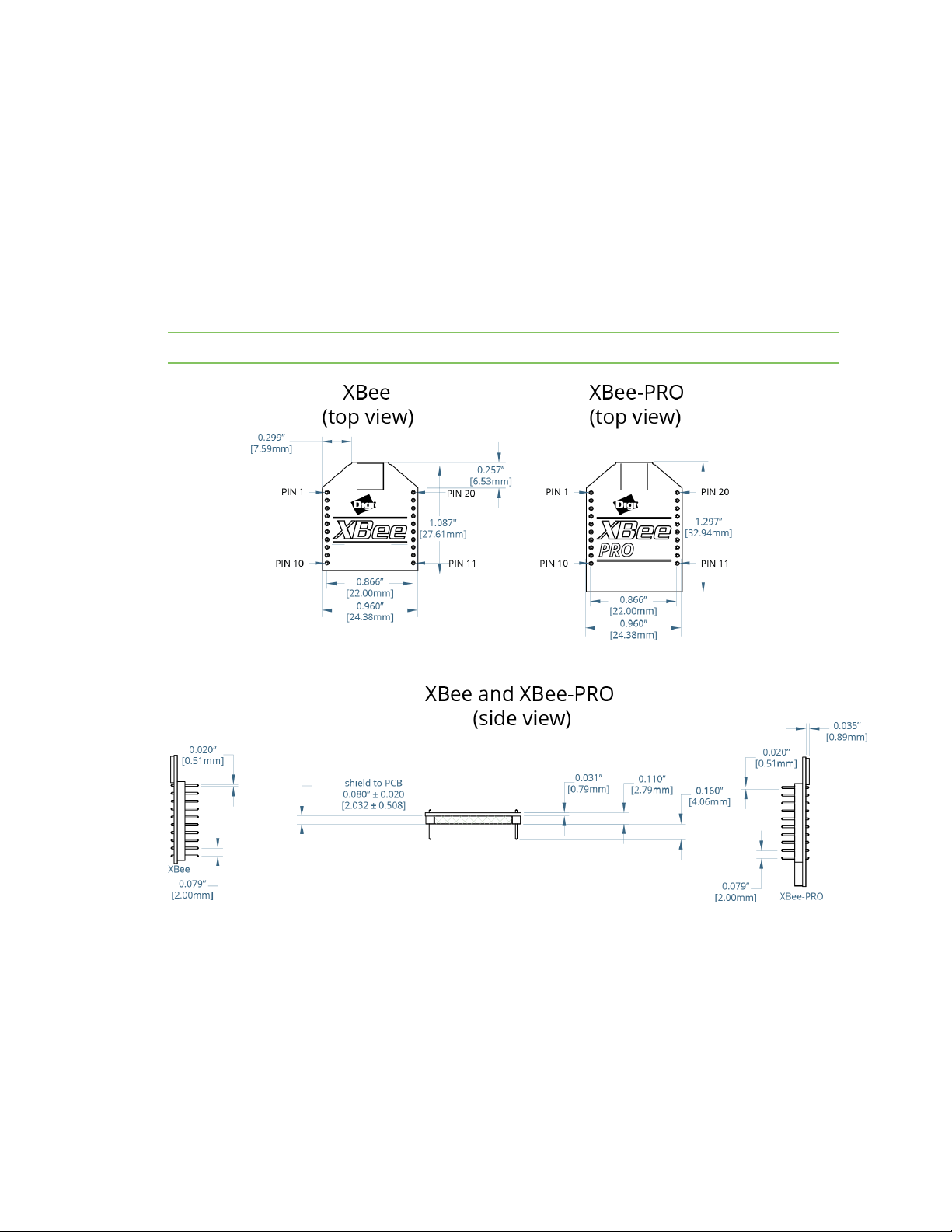
XBee/XBee-PRO S1 802.15.4 (Legacy) Mechanical drawings
The following graphics show the mechanical drawings of the XBee / XBee-PRO OEM RF Modules. The
XBee and XBee-PRO RF Modules are pin-for-pin compatible.
Note The antenna options not shown.
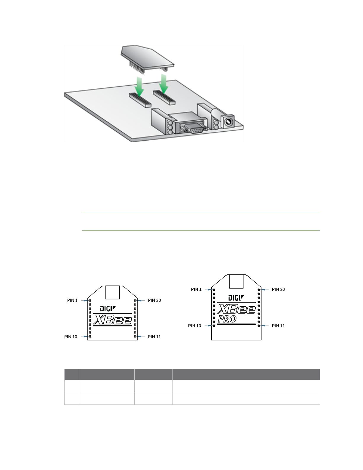
Mounting considerations
We design the through-hole module to mount into a receptacle so that you do not have to solder the
module when you mount it to a board. The development kits may contain RS-232 and USB interface
boards that use two 20-pin receptacles to receive modules.
The following illustration shows the module mounting into the receptacle on the RS-232 interface
board.
XBee/XBee-PRO S1 802.15.4 (Legacy) User Guide
16
Page 17
Hardware Pin signals
Century Interconnect manufactures the receptacles used on Digi development boards. Several other
manufacturers provide comparable mounting solutions; however, Digi currently uses the following
receptacles:
n Through-hole single-row receptacles: Samtec part number: MMS-110-01-L-SV (or equivalent)
n Surface-mount double-row receptacles: Century Interconnect part number: CPRMSL20-D-0-1
(or equivalent)
n Surface-mount single-row receptacles: Samtec part number: SMM-110-02-SM-S
Note We recommend that you print an outline of the module on the board to indicate the
correct orientation for mounting the module.
Pin signals
The following image shows the pin numbers; it shows the device's top sides, the shields are on the
bottom.
The following table describes the pin assignments for the devices. A horizontal line above the signal
name indicates low-asserted signals.
Pin Name Direction Description
1
VCC - Power supply
2
DOUT Output UART data out
XBee/XBee-PRO S1 802.15.4 (Legacy) User Guide
17
Page 18

Hardware Pin signals
Pin Name Direction Description
3 DIN/CONFIG
DO8
1
4
5 RESET
Input UART data In
Either Digital output 8
Input/Open
drain output
Device reset (reset pulse must be at least 200 ns). This
must be driven as an open drain/collector. The device
drives this line low when a reset occurs. Never drive this
line high.
6
PWM0/RSSI Either PWM output 0 / RX signal strength indicator
7
PWM1 Either PWM output 1
8
[reserved] - Do not connect
9 DTR/SLEEP_RQ/DI8
10
GND - Ground
11
AD4/DIO4 Either Analog input 4 or digital I/O 4
12 CTS /DIO7
13 ON/SLEEP
14
VREF Input Voltage reference for A/D inputs
15
Associate/AD5/DIO5 Either Associated indicator, analog input 5 or digital I/O 5
Either Pin sleep control line or digital input 8
Either Clear-to-send flow control or digital I/O 7
Output Device status indicator
16 RTS/DIO6
17
AD3/DIO3 Either Analog input 3 or digital I/O 3
18
AD2/DIO2 Either Analog input 2 or digital I/O 2
19
AD1/DIO1 Either Analog input 1 or digital I/O 1
20
AD0/DIO0 Either Analog input 0, digital I/O 0
Either Request-to-send flow control, or digital I/O 6
Notes:
n Minimum connections: VCC, GND, DOUT and DIN
n Minimum connections for updating firmware: VCC, GND, DIN, DOUT, RTS and DTR
n Signal direction is specified with respect to the module
n The module includes a 50 kΩ pull-up resistor attached to RESET
n You can configure several of the input pull-ups using the PR command
n Leave any unused pins disconnected
1
Function is not supported at the time of this release.
XBee/XBee-PRO S1 802.15.4 (Legacy) User Guide
18
Page 19

Hardware Design notes
Design notes
The XBee modules do not specifically require any external circuitry specific connections for proper
operation. However, there are some general design guidelines that we recommend for help in
troubleshooting and building a robust design.
Power supply design
A poor power supply can lead to poor device performance, especially if you do not keep the supply
voltage within tolerance or if it is excessively noisy. To help reduce noise, place a 1.0 μF and 8.2 pF
capacitor as near as possible to pin 1 on the PCB. If you are using a switching regulator for the power
supply, switch the frequencies above 500 kHz. Limit the power supply ripple to a maximum 100 mV
peak to peak.
Board layout
We design XBee devices to be self sufficient and have minimal sensitivity to nearby processors,
crystals or other printed circuit board (PCB) components. Keep power and ground traces thicker than
signal traces and make sure that they are able to comfortably support the maximum current
specifications. There are no other special PCB design considerations to integrate XBee devices, with
the exception of antennas.
Antenna performance
Antenna location is important for optimal performance. The following suggestions help you achieve
optimal antenna performance. Point the antenna up vertically (upright). Antennas radiate and receive
the best signal perpendicular to the direction they point, so a vertical antenna's omnidirectional
radiation pattern is strongest across the horizon.
Position the antennas away from metal objects whenever possible. Metal objects between the
transmitter and receiver can block the radiation path or reduce the transmission distance. Objects
that are often overlooked include:
n metal poles
n metal studs
n structure beams
n concrete, which is usually reinforced with metal rods
If you place the device inside a metal enclosure, use an external antenna. Common objects that have
metal enclosures include:
n vehicles
n elevators
n ventilation ducts
n refrigerators
n microwave ovens
n batteries
n tall electrolytic capacitors
Do not place XBee devices with the chip or integrated PCB antenna inside a metal enclosure.
Do not place any ground planes or metal objects above or below the antenna.
XBee/XBee-PRO S1 802.15.4 (Legacy) User Guide
19
Page 20
Hardware Design notes
For the best results, mount the device at the edge of the host PCB. Ensure that the ground, power,
and signal planes are vacant immediately below the antenna section.
Pin connection recommendations
The only required pin connections are VCC, GND, DOUT and DIN. To support serial firmware updates,
you should connect VCC, GND, DOUT, DIN, RTS, and SLEEP (DTR).
Leave all unused pins disconnected. Pull all inputs on the device high with internal pull-up resistors
using the PR command. You do not need a specific treatment for unused outputs.
Other pins may be connected to external circuitry for convenience of operation including the Associate
LED pin (pin 15). The Associate LED flashes differently depending on the state of the device.
If analog sampling is desired, attach the VRef (pin 14) to a voltage reference.
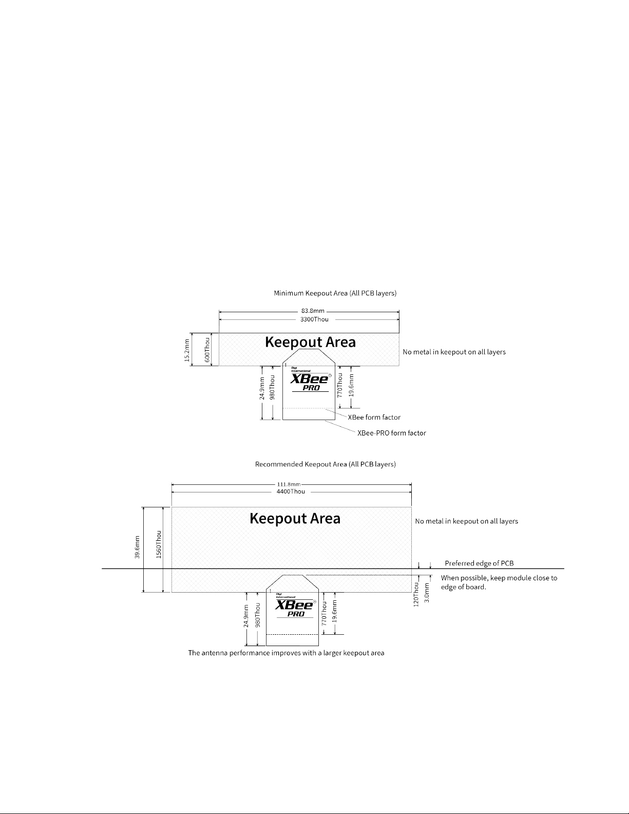
Keepout area
We recommend that you allow a “keepout” area, as shown in the following drawing.
XBee/XBee-PRO S1 802.15.4 (Legacy) User Guide
20
Page 21

Hardware Design notes
Notes
1. We recommend non-metal enclosures. For metal enclosures, use an external antenna.
2. Keep metal chassis or mounting structures in the keepout area at least 2.54 cm (1 in) from the
antenna.
3. Maximize the distance between the antenna and metal objects that might be mounted in the
keepout area.
4. These keepout area guidelines do not apply for wire whip antennas or external RFconnectors.
Wire whip antennas radiate best over the center of a ground plane.
XBee/XBee-PRO S1 802.15.4 (Legacy) User Guide
21
Page 22

Operation
Serial communications 23
ADC and Digital I/O line support 26
Networks 30
Addressing 34
Modes of operation 35
Multiple AT commands 41
Parameter format 41
XBee/XBee-PRO S1 802.15.4 (Legacy) User Guide
22
Page 23
Operation Serial communications
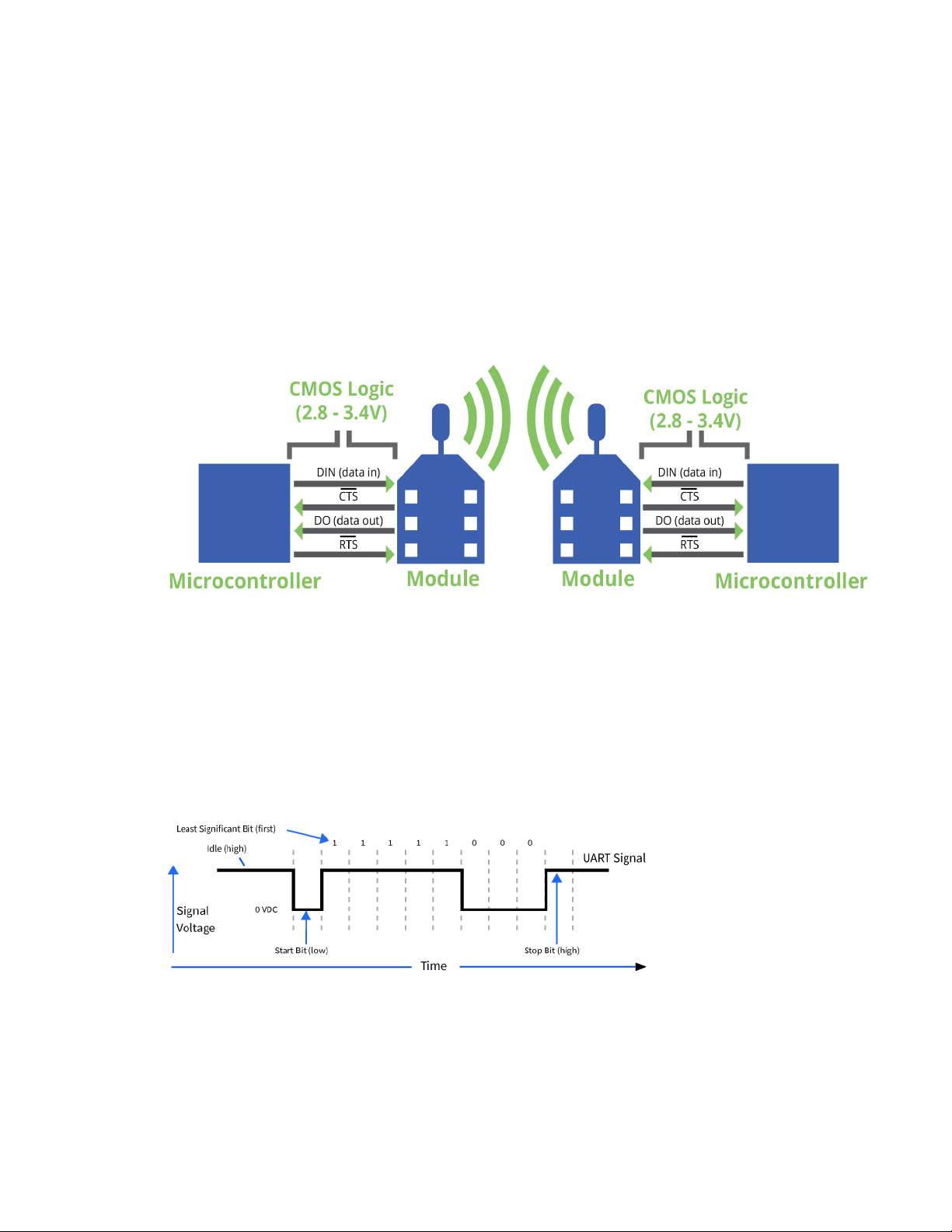
Serial communications
RF Modules interface to a host device through a serial port. Using its serial port, the device
communicates with any of the following:
n Logic and voltage compatible UART
n Level translator to any serial device (for example, through an RS-232 or USB interface board)
UART data flow
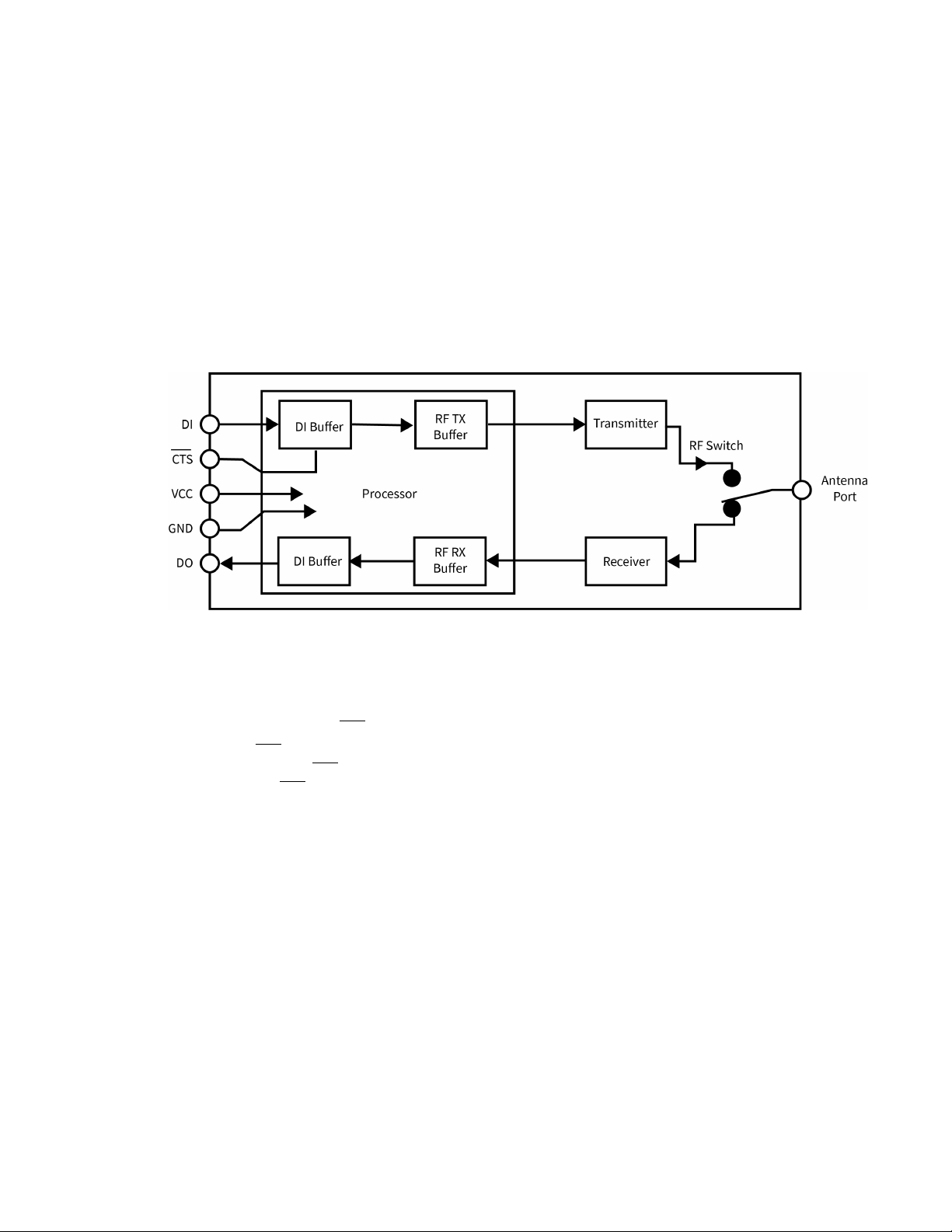
Devices that have a UART interface connect directly to the pins of the XBee/XBee-PRO S1 802.15.4
(Legacy) as shown in the following figure. The figure shows system data flow in a UART-interfaced
environment. Low-asserted signals have a horizontal line over the signal name.
Serial data
A device sends data to the XBee/XBee-PRO S1 802.15.4 (Legacy)'s UART through pin 3 DIN as an
asynchronous serial signal. When the device is not transmitting data, the signals should idle high.
For serial communication to occur, you must configure the UART of both devices (the microcontroller
and the XBee/XBee-PRO S1 802.15.4 (Legacy)) with compatible settings for the baud rate, parity, start
bits, stop bits, and data bits.
Each data byte consists of a start bit (low), 8 data bits (least significant bit first) and a stop bit (high).
The following diagram illustrates the serial bit pattern of data passing through the device. The
diagram shows UART data packet 0x1F (decimal number 31) as transmitted through the device.
Serial communications depend on the two UARTs (the microcontroller and the RF device) to be
configured with compatible settings, including baud rate, parity, start bits, stop bits, and data bits.
The UART baud rate and parity settings on the XBee module can be configured with the BD and NB
commands, respectively. For more information, see AT commands.
XBee/XBee-PRO S1 802.15.4 (Legacy) User Guide
23
Page 24

Operation Serial communications
Transparent operating mode
Devices operate in this mode by default. The device acts as a serial line replacement when it is in
Transparent operating mode. The device queues all UART data it receives through the DIN pin for RF
transmission. When a device receives RF data, it sends the data out through the DOUT pin. You can set
the configuration parameters using Command mode.
Serial-to-RF packetization
The device buffers data in the serial receive buffer until one of the following causes the data to be
packetized and transmitted:
n The device receives no serial characters for the amount of time determined by the RO
(Packetization Timeout) parameter. If RO = 0, packetization begins when a character is
received.
n The device receives the Command Mode Sequence (GT + CC + GT). Any character buffered in
the serial receive buffer before the sequence is transmitted.
n The device receives the maximum number of characters that fits in an RF packet (100 bytes).
If the device cannot immediately transmit (for example, if it is already receiving RF data), it stores the
serial data in the DI buffer. The device packetizes the data and sends the data at any RO timeout or
when it receives the maximum packet size (100 bytes).
If the DI buffer becomes full, hardware or software flow control must be implemented in order to
prevent overflow (that is, loss of data between the host and module).
API operating mode
API (Application Programming Interface) operating mode is an alternative to the default Transparent
operating mode. The frame-based API extends the level to which a host application can interact with
the networking capabilities of the module.
When in API mode, all data entering and leaving the device is contained in frames that define
operations or events within the module.
Transmit data frames (received through the DI pin (pin 3)) include:
n RF Transmit data frame
n Command frame (equivalent to AT commands)
Receive Data frames (sent out the DO pin (pin 2)) include:
n RF-received data frame
n Command response
n Event notifications such as reset, associate, disassociate, and so on
The API provides alternative means of configuring modules and routing data at the host application
layer. A host application sends data frames to the device that contains address and payload
information instead of using command mode to modify addresses. The device sends data frames to
the application containing status packets, as well as source, RSSI, and payload information from
received data packets.
The API operation option facilitates many operations such as the following examples:
XBee/XBee-PRO S1 802.15.4 (Legacy) User Guide
24
Page 25
Operation Serial communications
n Transmitting data to multiple destinations without entering Command Mode
n Receiving success/failure status of each transmitted RF packet
n Identifying the source address of each received packet
To implement API operation, see API operation.
Flow control
The XBee/XBee-PRO S1 802.15.4 (Legacy) maintains buffers to collect serial and RF data that it
receives. The serial receive buffer collects incoming serial characters and holds them until the device
can process them. The serial transmit buffer collects the data it receives via the RF link until it
transmits that data out the serial port. The following figure shows the process of device buffers
collecting received serial data.
DI (Data in) buffer
When serial data enters the RF module through the DI pin (pin 3), the device stores data in the DI
buffer until it can be processed.
Hardware Flow Control (CTS)
If you enable CTS flow control (by setting D7 to 1), when the DI buffer is 17 bytes away from being full,
the device de-asserts CTS (sets it high) to signal to the host device to stop sending serial data. The
device reasserts CTS after the serial receive buffer has 34 bytes of space.
To eliminate the need for flow control:
1. Send messages that are smaller than the DI buffer size (202 bytes).
2. Interface at a lower baud rate [BD (Interface Data Rate) parameter] than the throughput data
rate.
Example where the DI buffer may become full and possibly overflow:
If the device is receiving a continuous stream of RF data, it places any serial data that arrives on the
DI pin in the DI buffer. The device transmits data in the DI buffer over-the-air when it is no longer
receiving RF data in the network.
For more information, see the following command descriptions:
n RO (Packetization Timeout)
n BD (Interface Data Rate)
n D7 (DIO7 Configuration)
XBee/XBee-PRO S1 802.15.4 (Legacy) User Guide
25
Page 26

Operation ADC and Digital I/O line support
DO (Data out) buffer
When RF data is received, the data enters the DO buffer and is sent out the serial port to a host
device. Once the DO Buffer reaches capacity, any additional incoming RF data is lost.
Hardware Flow Control (RTS)
If you enable RTS flow control (D6 (DIO6 Configuration) Parameter = 1), the device does not send data
out the DO buffer as long as RTS (pin 16) is de-asserted.
Examples where the DO buffer may become full, resulting in dropped RF packets:
1. If the RF data rate is set higher than the interface data rate of the device, the device may
receive data faster than it can send the data to the host. Even occasional transmissions from a
large number of devices can quickly accumulate and overflow the transmit buffer.
2. If the host does not allow the device to transmit data out from the serial transmit buffer due to
being held off by hardware flow control.
See the D6 (DIO6 Configuration) command description for more information.
ADC and Digital I/O line support
The XBee/XBee-PRO RF Modules support ADC (analog-to-digital conversion) and digital I/O line
passing. The following pins support multiple functions:
n Pin functions and their associated pin numbers and commands
n AD = Analog-to-Digital Converter, DIO = Digital Input/Output
Note Pin functions in parentheses are not applicable to this section.
Pin function Pin# AT Command
AD0/DIO0 20
AD1/DIO1 19
AD2/DIO2 18
AD3/DIO3 / (COORD_SEL) 1
AD4/DIO4 11
AD5/DIO5 / (ASSOCIATE) 15
DIO6/(RTS) 16
DIO7/(CTS) 12
DI8/(DTR) / (Sleep_RQ) 9
Use the following setting to enable ADC and DIO pin functions:
D0
D1
D2
D3
D4
D5
D6
D7
D8
Support type Setting
ADC support ATDn = 2
XBee/XBee-PRO S1 802.15.4 (Legacy) User Guide
26
Page 27
Operation ADC and Digital I/O line support
Support type Setting
Digital input support ATDn = 3
Digital output low support ATDn = 4
Digital output high support ATDn = 5
I/O data format
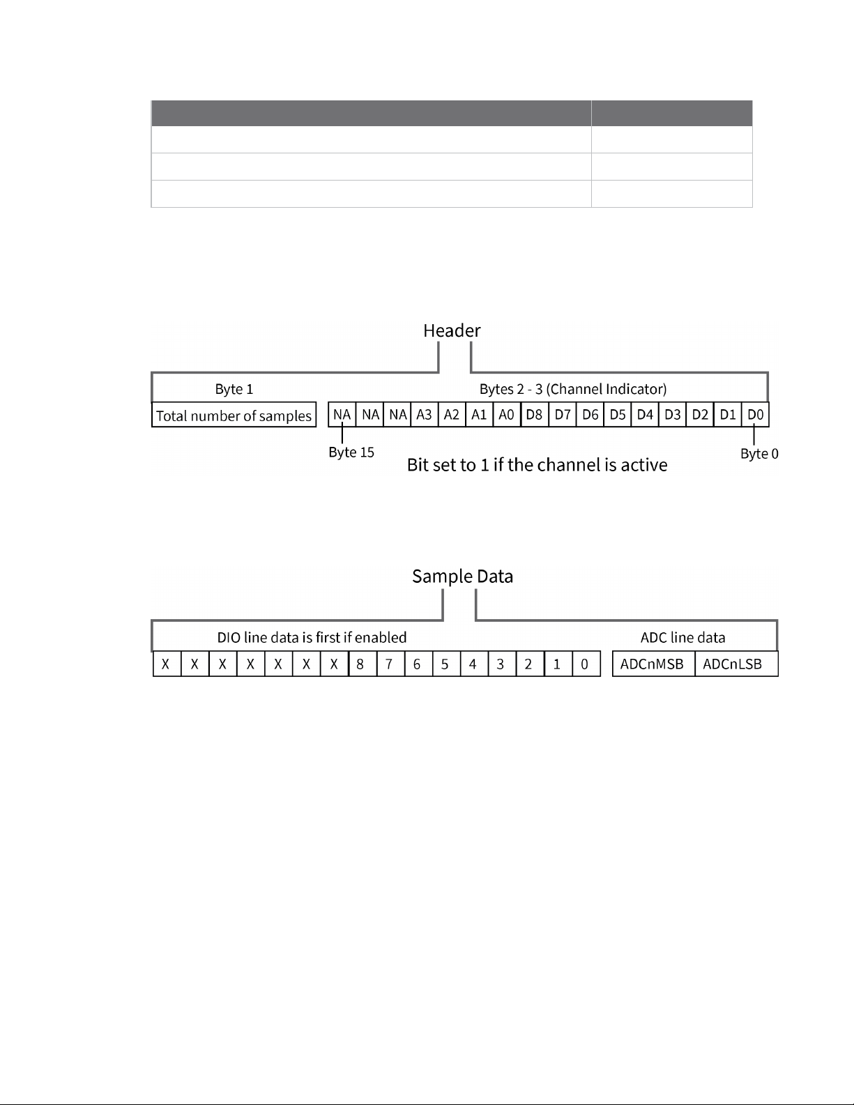
I/O data begins with a header. The first byte of the header defines the number of samples
forthcoming. The last two bytes of the header (Channel Indicator) define which inputs are active. Each
bit represents either a DIO line or ADC channel. The following figure illustrates the bits in the header.
Sample data follows the header and the channel indicator frame determines how to read the sample
data. If any of the DIO lines are enabled, the first two bytes are the DIO sample. The ADC data follows.
ADC channel data is represented as an unsigned 10-bit value right-justified on a 16- bit boundary. The
following figure illustrates the sample data bits.
API support
I/O data is sent out the UART using an API frame. All other data can be sent and received using
Transparent Operation or API frames if API mode is enabled (AP > 0).
API Operations support two RX (Receive) frame identifiers for I/O data (set 16-bit address to 0xFFFE
and the device does 64-bit addressing):
n 0x82 for RX Packet: 64-bit Address I/O
n 0x83 for RX Packet: 16-bit Address I/O
The API command header is the same as shown in 64-bit Receive Packet - 0x80 and 16-bit I/O Sample
Indicator - 0x83. RX data follows the format described in I/O data format.
Sleep support
Set SO (Sleep Options) bit 1 to suppress automatic wake-up sampling.
XBee/XBee-PRO S1 802.15.4 (Legacy) User Guide
27
Page 28

Operation ADC and Digital I/O line support
When a device wakes, it always performs a sample based on any active ADC or DIO lines. This allows
sampling based on the sleep cycle whether it be Cyclic Sleep (SM = 4 or 5) or Pin Sleep (SM = 1). Set
the IR (Sample Rate) parameter to gather more samples when awake.
For Cyclic Sleep modes: If the IR parameter is set, the device stays awake until the IT (Samples before
TX) parameter is met. The device stays awake for ST (Time before Sleep).
DIO pin change detect
When you use the IC (DIOChange Detect) command to enable DIO Change Detect, DIO lines 0 - 7 are
monitored. When a change is detected on a DIO line, the following occurs:
1. An RF packet is sent with the updated DIO pin levels. This packet does not contain any ADC
samples.
2. Any queued samples are transmitted before the change detect data. This may result in
receiving a packet with less than IT (Samples before TX) samples.
Note Change detect does not affect Pin Sleep wake-up. The D8 pin (DTR/Sleep_RQ/DI8) is the only line
that wakes a device from Pin Sleep. If not all samples are collected, the device still enters Sleep Mode
after a change detect packet is sent. Change detect is only supported when the Dx (DIOx
Configuration) parameter equals 3, 4 or 5.
Applicable Commands: IC (DIO Change Detect), IT (Samples before TX)
Note Change detect is only supported when the Dx (DIOx Configuration) parameter equals 3, 4 or 5.
Sample rate (interval)
The Sample Rate (Interval) feature allows enabled ADC and DIO pins to be read periodically on devices
that are not configured to operate in Sleep Mode. When one of the Sleep Modes is enabled and the IR
(Sample Rate) parameter is set, the device stays awake until IT (Samples before TX) samples have
been collected.
Once a particular pin is enabled, the appropriate sample rate must be chosen. The maximum sample
rate that can be achieved while using one A/D line is 1 sample/ms or 1 kHz. The device cannot keep up
with transmission when IR and IT are equal to 1 and we do not recommend configuring the device to
sample at rates greater than once every 20 ms.
I/O line passing
You can set up virtual wires between XBee/XBee-PRO Modules. When a device receives an RF data
packet that contains I/O data, it can be setup to update any enabled outputs (PWM and DIO) based on
the data it receives.
I/O lines are mapped in pairs. For example, AD0 can only update PWM0 and DI5 can only update DO5.
The default setup is for outputs not to be updated, which results in the I/O data being sent out the
UART (See the IU (I/O Output Enable) command). To enable the outputs for updating, set the IA (I/O
Input Address) parameter with the address of the device that has the appropriate inputs enabled. This
binds the outputs to a particular device's input. This does not affect the ability of the device to receive
I/O line data from other modules; if affects only its ability to update enabled outputs. The IA
parameter can also be set up to accept I/O data for output changes from any module by setting the IA
parameter to 0xFFFF.
When outputs are changed from their non-active state, the device can be setup to return the output
level to its non-active state. Set the timers using the Tn (Dn Output Timer) and PT (PWM Output
XBee/XBee-PRO S1 802.15.4 (Legacy) User Guide
28
Page 29

Operation ADC and Digital I/O line support
Timeout) commands. The timers are reset every time the device receives a valid I/O sample packet
with a matching IA address.
You can adjust the IC (Change Detect) and IR (Sample Rate) parameters to keep the outputs set to
their active output if the system needs more time than the timers can handle.
Note DI8 cannot be used for I/O line passing.
XBee/XBee-PRO S1 802.15.4 (Legacy) User Guide
29
Page 30

Operation Networks
Applicable commands:
n IA (I/O Input Address)
n TN (Dn Output Timeout)
n P0 (PWM0 Configuration)
n P1 (PWM1 Configuration)
n M0 (PWM0 Output Level)
n M1 (PWM1 Output Level)
n PT (PWM Output Timeout)
n RP (RSSSI PWM Timer)
Configuration example
The following table provides an example of a pair of RF devices for a simple A/D link:
Remote Configuration Base Configuration
DL = 0x1234 DL = 0x5678
MY = 0x5678 MY = 0x1234
D0 = 2 P0 = 2
D1 = 2 P1 = 2
IR = 0x14 IU = 1
IT = 5 IA = 0x5678 (or 0xFFFF)
These settings configure the remote device to sample AD0 and AD1 once each every 20 ms. It then
buffers 5 samples each before sending them back to the base device. The base then receives a 32byte transmission (20 bytes data and 12 bytes framing) every 100 ms.
Networks
The following table describes some common terms we use when discussing networks.
Term Definition
Association Establishing membership between end devices and a coordinator.
Coordinator A full-function device (FFD) that provides network synchronization by polling nodes.
End device When in the same network as a coordinator. Devices that rely on a coordinator for
synchronization and can be put into states of sleep for low-power applications.
PAN Personal Area Network. A data communication network that includes one or more
end devices and optionally a coordinator.
XBee/XBee-PRO S1 802.15.4 (Legacy) User Guide
30
Page 31

Operation Networks
Peer-to-peer networks
By default, XBee/XBee-PRO S1 802.15.4 (Legacy) modules are configured to operate within a peer-topeer network topology and therefore are not dependent upon master/slave relationships. This means
that devices remain synchronized without the use of master/server configurations and each device in
the network shares both roles of master and slave. Our peer-to-peer architecture features fast
synchronization times and fast cold start times. This default configuration accommodates a wide
range of RF data applications.
You can establish a peer-to-peer network by configuring each module to operate as an End Device (CE
= 0), disabling End Device Association on all modules (A1 = 0) and setting ID and CH parameters to be
identical across the network.
NonBeacon (with coordinator)
You can configure a device as a Coordinator by setting the CE (Coordinator Enable) parameter to 1.
Use the A2 (Coordinator Association) parameter to power up the Coordinator .
In a Coordinator system, you configure the Coordinator to use direct or indirect transmissions. If the
SP (Cyclic Sleep Period) parameter is set to 0, the Coordinator sends data immediately. Otherwise,
the SP parameter determines the length of time the Coordinator retains the data before discarding it.
In general, SP (Cyclic Sleep Period) and ST (Time before Sleep) parameters should be set to match the
SP and ST settings of the End Devices.
Association
Association is the establishment of membership between End Devices and a Coordinator. Establishing
membership is useful in scenarios that require a central unit (Coordinator) to relay messages to or
gather data from several remote units (End Devices), assign channels, or assign PAN IDs.
An RF data network that consists of one Coordinator and one or more End Devices forms a PAN
(Personal Area Network). Each device in a PAN has a PAN Identifier (ID (PAN ID) parameter), which
must be unique to prevent miscommunication between PANs. Set the Coordinator PAN ID using the ID
(PAN ID) and A2 (Coordinator Association) commands.
An End Device can associate to a Coordinator without knowing the address, PAN ID, or channel of the
Coordinator. The A1 (End Device Association) parameter bit fields determine the flexibility of an End
Device during association. Use the A1 parameter for an End Device to dynamically set its destination
address, PAN ID, and/or channel.
For example, if the PAN ID of a Coordinator is known, but the operating channel is not, set the A1
command on the End Device to enable the ‘Auto_Associate’ and ‘Reassign_Channel’ bits. Additionally,
set the ID parameter to match the PAN ID of the associated Coordinator.
Coordinator / End Device setup and operation
To configure a module to operate as a Coordinator, set the CE (Coordinator Enable) parameter to ‘1’.
Set the CE parameter of End Devices to ‘0’ (default). Coordinator and End Devices should contain
matching firmware versions.
XBee/XBee-PRO S1 802.15.4 (Legacy) User Guide
31
Page 32

Operation Networks
NonBeacon (with Coordinator) systems
You can configure the Coordinator to use direct or indirect transmissions. If the SP (Cyclic Sleep
Period) parameter is set to ‘0’, the Coordinator sends data immediately. Otherwise, the SP parameter
determines the length of time the Coordinator retains the data before discarding it. In general, SP
(Cyclic Sleep Period) and ST (Time before Sleep) parameters should be set to match the SP and ST
settings of the End Devices.
Coordinator start-up
The A2 (Coordinator Association) command governs coordinator power-up. On power-up, the
Coordinator undergoes the following sequence of events:
1. Check A2 parameter- Reassign_PANID flag
Set (bit 0 = 1)
The Coordinator issues an Active Scan. The Active Scan selects one channel and transmits a request to
the broadcast address (0xFFFF) and broadcast PAN ID (0xFFFF). The Coordinator then listens on that
channel for beacons from any Coordinator operating on that channel. The SD (Scan Duration)
parameter value determines the listen time on each channel.
Once the time expires on that channel, the Active Scan selects another channel and again transmits
the BeaconRequest as before. This process continues until all channels have been scanned, or until 5
PANs have been discovered. When the Active Scan is complete, the results include a list of PAN IDs and
Channels being used by other PANs. This list is used to assign an unique PAN ID to the new
Coordinator. The ID parameter will be retained if it is not found in the Active Scan results. Otherwise,
the ID (PAN ID) parameter setting will be updated to a PAN ID that was not detected.
Not set (bit 0 = 0)
The Coordinator retains its ID setting. No Active Scan is performed.
2. Check A2 parameter - Reassign_Channel flag (bit 1)
Set (bit 1 = 1)
The Coordinator issues an Energy Scan. The Energy Scan selects one channel and scans for energy on
that channel. The SD (Scan Duration) parameter specifies the duration of the scan. Once the scan is
completed on a channel, the Energy Scan selects the next channel and begins a new scan on that
channel. This process continues until all channels have been scanned.
When the Energy Scan is complete, the results include the maximal energy values detected on each
channel. This list is used to determine a channel where the least energy was detected. If an Active
Scan was performed (Reassign_PANID Flag set), the channels used by the detected PANs are
eliminated as possible channels. The device uses the results of the Energy Scan and the Active Scan (if
performed) to find the best channel (that is, the channel with the least energy that is not used by any
detected PAN). Once the device selects the best channel, the CH (Channel) parameter value is
updated to that channel.
Not set (bit 1 = 0)
The Coordinator retains its CH setting, and an Energy Scan is not performed.
3. Start Coordinator
The Coordinator starts on the specified channel (CH parameter) and PAN ID (ID parameter).
Note These may be selected in steps 1 or 2.
XBee/XBee-PRO S1 802.15.4 (Legacy) User Guide
32
Page 33

Operation Networks
The Coordinator only allows End Devices to associate to it if the A2 parameter “AllowAssociation” flag
is set. Once the Coordinator has successfully started, the Associate LED blinks 1 time per second. If
the Coordinator has not started, the LED is solid.
4. Modify coordinator
Once a Coordinator has started, modifying the A2 (Reassign_Channel or Reassign_PANID bits), ID, CH
or MY parameters causes the Coordinator’s MAC to reset. The Coordinator RF module (including
volatile RAM) is not reset.
Changing the A2 AllowAssociation bit does not reset the Coordinator’s MAC. In a non-beaconing
system, End Devices that associated to the Coordinator prior to a MAC reset have knowledge of the
new settings on the Coordinator. If the Coordinator were to change its ID, CH or MY settings, the End
Devices would no longer be able to communicate with the non-beacon Coordinator. Do not change the
ID, CH, MY, or A2 (Reassign_Channel or Reassign_PANID bits) once a Coordinator has started.
End device start-up
The A1 (End Device Association) command governs End Device power-up. On power-up, the End Device
undergoes the following sequence of events:
1. Check A1 parameter - AutoAssociate Bit
Set (bit 2 = 1)
The End Device attempts to associate to a Coordinator. See 2. Discover Coordinator (if Auto-Associate
Bit Set) and 3. Associate to a valid coordinator.
Not set (bit 2 = 0)
The End Device does not attempt to associate to a Coordinator. The End Device operates as specified
by its ID, CH and MY parameters. Association is considered complete and the Associate LED blinks
quickly (5 times per second).
2. Discover Coordinator (if Auto-Associate Bit Set)
The end device issues an Active Scan. The Active Scan selects one channel and transmits a
BeaconRequest command to the broadcast address (0xFFFF) and broadcast PAN ID (0xFFFF). The
Active Scan then listens on that channel for beacons from any Coordinator operating on that channel.
The SD parameter determines the listen time on each channel.
Once the time expires on that channel, the Active Scan selects another channel and again transmits
the BeaconRequest command as before. This process continues until all channels have been scanned,
or until 5 PANs have been discovered. When the Active Scan is complete, the results include a list of
PAN IDs and Channels that are being used by detected PANs.
The end device selects a coordinator to associate with according to the A1 parameter “Reassign_
PANID” and “Reassign_Channel” flags:
n Reassign_PANID bit set (bit 0 = 1) - End device can associate with a PAN with any ID value.
n Reassign_PANID bit not set (bit 0 = 0) - End device only associates with a PAN whose ID
setting matches the ID setting of the End Device.
n Reassign_Channel bit set (bit 1 = 1) - End device can associate with a PAN with any CH
value.
n Reassign_Channel bit not set (bit 1 = 0) - End device will only associate with a PAN whose
CH setting matches the CH setting of the end device.
After applying these filters to the discovered coordinators, if multiple candidate PANs exist, the end
device selects the PAN whose transmission link quality is the strongest. If no valid coordinator is
XBee/XBee-PRO S1 802.15.4 (Legacy) User Guide
33
Page 34

Operation Addressing
found, the end device either goes to sleep (as dictated by its SM (Sleep Mode) parameter) or retry
Association.
Note An end device also disqualifies coordinators if they are not allowing association (A2 -
AllowAssociation bit), or, if the coordinator is not using the same NonBeacon scheme as the end
device. They must both be programmed with NonBeacon code.
3. Associate to a valid coordinator
Once the device finds a valid coordinator (2. Discover Coordinator (if Auto-Associate Bit Set)), the end
device sends an AssociationRequest message to the coordinator. The end device then waits for an
AssociationConfirmation from the coordinator. Once it receives the Confirmation, the end device is
Associated and the Associate LED blinks rapidly (two times per second). If the end device has not
associated, the LED is solid.
4. End Device changes once an End Device has associated
Changing A1, ID or CH parameters causes the End Device to disassociate and restart the Association
procedure.
If the End Device fails to associate, the AI command indicates the failure.
Addressing
Every RF data packet sent over-the-air contains a Source Address and Destination Address field in its
header. The XBee/XBee-PRO S1 802.15.4 (Legacy) conforms to the 802.15.4 specification and supports
both short 16-bit addresses and long 64-bit addresses. A unique 64-bit IEEE source address is assigned
at the factory and can be read with the SL (Serial Number Low) and SH (Serial Number High)
commands. You must manually configure short addressing. A device uses its unique 64-bit address as
its Source Address if its MY (16-bit Source Address) value is 0xFFFF or 0xFFFE.
n To send a packet to a specific device using 64-bit addressing, set the Destination Address (DL +
DH) of the sender to match the Source Address (SL + SH) of the intended destination device.
n To send a packet to a specific module using 16-bit addressing, set DL (Destination Address
Low) parameter to equal the MY parameter of the intended destination module and set the DH
(Destination Address High) parameter to '0.'
Unicast mode
By default, the XBee/XBee-PRO S1 802.15.4 (Legacy) operates in Unicast mode. Unicast Mode is the
only mode that supports retries. While in this mode, receiving devices send an ACK (acknowledgment)
of RF packet reception to the transmitter. If the transmitting device does not receive the ACK, it resends the packet up to three times or until it receives the ACK.
Short 16-bit addresses
You can configure the device to use short 16-bit addresses as the Source Address by setting (MY <
0xFFFE). Setting the DH parameter (DH = 0) configures the Destination Address to be a short 16-bit
address (if DL < 0xFFFE). For two devices to communicate using short addressing, the Destination
Address of the transmitter device must match the MY parameter of the receiver.
The following table shows a sample network configuration that enables Unicast mode
communications using short 16-bit addresses.
XBee/XBee-PRO S1 802.15.4 (Legacy) User Guide
34
Page 35

Operation Modes of operation
Parameter RF device 1 RF device 2
MY (Source Address)
DH (Destination Address High)
DL (Destination Address Low)
0x01 0x02
0 0
0x02 0x01
Long 64-bit addresses
You can use The RF device’s serial number (SL parameter concatenated to the SH parameter) as a 64bit source address when the MY (16-bit Source Address) parameter is disabled. When you disable the
MY parameter (MY = 0xFFFF or 0xFFFE), the device’s source address is set to the 64-bit IEEE address
stored in the SH and SL parameters.
When an End Device associates to a Coordinator, its MY parameter is set to 0xFFFE to enable 64-bit
addressing. The 64-bit address of the device is stored as SH and SL parameters. To send a packet to a
specific device, the Destination Address (DL + DH) on the sender must match the Source Address (SL +
SH) of the receiver.
Broadcast mode
Any RF device within range accepts a packet that contains a broadcast address. When configured to
operate in Broadcast Mode, receiving devices do not send ACKs (acknowledgments) and transmitting
devices do not automatically re-send packets as is the case in Unicast Mode.
To send a broadcast packet to all devices regardless of 16-bit or 64-bit addressing, set the destination
addresses of all the devices as shown below.
Sample Network Configuration (All modules in the network):
n DL (Destination Low Address) = 0x0000FFFF
If RR is set to 0, only one packet is broadcast. If RR > 0, (RR + 2) packets are sent in each broadcast.
No acknowledgments are returned. For more information, see RR (XBee Retries).
n DH (Destination High Address) = 0x00000000 (default value)
When you are programming the device, enter the parameters in hexadecimal notation (without the
“0x” prefix). Leading zeros may be omitted.
Modes of operation
This section describes the different operating modes for the device.
XBee/XBee-PRO S1 802.15.4 (Legacy) User Guide
35
Page 36

Operation Modes of operation
Idle mode
When not receiving or transmitting data, the device is in Idle mode.
The device shifts into the other modes of operation under the following conditions:
n Transmit mode (serial data is received in the DI buffer).
n Receive mode (valid RF data received through the antenna).
n Sleep mode (Sleep mode condition is met).
n Command mode (Command mode sequence issued).
Transmit/Receive modes
This section provides information about the different types of transmit and receive modes.
RF data packets
Each transmitted data packet contains a Source Address and Destination Address field. The Source
Address matches the address of the transmitting device as specified by the MY (Source Address)
parameter (if MY ≥ 0xFFFE), the SH (Serial Number High) parameter or the SL (Serial Number Low)
parameter. The <Destination Address> field is created from the DH (Destination Address High) and DL
(Destination Address Low) parameter values. The Source Address and/or Destination Address fields
either contain a 16-bit short or long 64-bit long address.
The RF data packet structure follows the 802.15.4 specification. For more information, see
Addressing.
Direct and indirect transmission
There are two methods to transmit data:
n Direct transmission: data is transmitted immediately to the Destination Address
n Indirect transmission: a packet is retained for a period of time and is only transmitted after the
destination device (source address = destination address) requests the data.
XBee/XBee-PRO S1 802.15.4 (Legacy) User Guide
36
Page 37

Operation Modes of operation
Indirect transmissions can only occur on a Coordinator. Thus, if all nodes in a network are End Devices,
only direct transmissions occurs. Indirect transmissions are useful to ensure packet delivery to a
sleeping node. The Coordinator currently is able to retain up to two indirect messages.
Direct transmission
A Coordinator can be configured to use only direct transmission by setting the SP (Cyclic Sleep Period)
parameter to 0. Also, a Coordinator using indirect transmissions reverts to direct transmission if it
knows the destination device is awake.
To enable this behavior, the ST (Time before Sleep) value of the Coordinator must be set to match the
ST value of the End Device. Once the End Device either transmits data to the Coordinator or polls the
Coordinator for data, the Coordinator uses direct transmission for all subsequent data transmissions
to that device address until ST time occurs with no activity (at which point it reverts to using indirect
transmissions for that device address). "No activity" means no transmission or reception of messages
with a specific address. Broadcast messages do not reset the ST timer.
Indirect transmission
To configure Indirect Transmissions in a Personal Area Network (PAN), the SP (Cyclic Sleep Period)
parameter value on the Coordinator must be set to match the longest sleep value of any End Device.
The sleep period value on the Coordinator determines how long (time or number of beacons) the
Coordinator retains an indirect message before discarding it.
An End Device must poll the Coordinator once it wakes from Sleep to determine if the Coordinator has
an indirect message for it. For Cyclic Sleep Modes, this is done automatically every time the device
wakes (after SP time). For Pin Sleep Modes, the A1 (End Device Association) parameter value must be
set to enable Coordinator polling on pin wake-up . Alternatively, an End Device can use the FP (Force
Poll) command to poll the Coordinator as needed.
Clear Channel Assessment (CCA)
Prior to transmitting a packet, the device performs a CCA (Clear Channel Assessment) on the channel
to determine if the channel is available for transmission. The detected energy on the channel is
compared with the CA (Clear Channel Assessment) parameter value. If the detected energy exceeds
the CA parameter value, the device does not transmit the packet.
Also, the device inserts a delay before a transmission takes place. You can set this delay using the RN
(Backoff Exponent) parameter. If you set RN to 0, then there is no delay before the first CCA is
performed. The RN parameter value is the equivalent of the “minBE” parameter in the 802.15.4
specification. The transmit sequence follows the 802.15.4 specification.
By default, the MM (MAC Mode) parameter = 0. On a CCA failure, the device attempts to re-send the
packet up to two additional times.
When in Unicast packets with RR (Retries) = 0, the device executes two CCA retries. Broadcast
packets always get two CCA retries.
Note Customers in Europe who have the XBee 802.15.4 module must manage their CCA settings. See
CA (CCA Threshold) for CA values.
Acknowledgment
If the transmission is not a broadcast message, the device expects to receive an acknowledgment
from the destination node. If an acknowledgment is not received, the packet is resent up to three
more times. If the acknowledgment is not received after all transmissions, an ACK failure is recorded.
XBee/XBee-PRO S1 802.15.4 (Legacy) User Guide
37
Page 38

Operation Modes of operation
Sleep modes
Sleep modes enable the device to enter states of low-power consumption when not in use. In order to
enter Sleep mode, one of the following conditions must be met (in addition to the device having a nonzero SM parameter value):
n SLEEP_RQ is asserted and the device is in a pin sleep mode (SM = 1, 2, or 5)
n The device is idle (no data transmission or reception) for the amount of time defined by the ST
(Time before Sleep) parameter.
Note ST is only active when SM = 4 or 5.
The following table shows the sleep mode configurations.
Transition
Sleep mode
setting
Transition
into sleep
mode
out of sleep
mode
(wake) Characteristics
Related
commands
Power
consumption
Pin hibernate
SM 1
Pin doze SM 2 Assert (high)
Cyclic Sleep
SM 4
Assert (high)
Sleep_RQ (pin
9)
Sleep_RQ (pin
9)
Automatic
transition to
Sleep Mode as
defined by the
SM (Sleep
Mode) and ST
(Time before
Sleep)
parameters
De-assert
(low) Sleep_
RQ
De-assert
(low) Sleep_
RQ
Transition
occurs after
the cyclic
sleep time
interval
elapses. The
time interval
is defined by
SP
the
(Cyclic Sleep
Period)
parameter.
Pin/Hostcontrolled/NonBeacon
systems only/Lowest
Power
Pin/Hostcontrolled/NonBeacon
systems only/Fastest
wake-up
RF module wakes in
pre-determined time
intervals to detect if
RF data is
present/When SM = 5
(SM
) < 10 µA (@3.0
VCC)
(SM) < 50 µA
(SM),SP,ST< 50 µA when
sleeping
XBee/XBee-PRO S1 802.15.4 (Legacy) User Guide
38
Page 39

Operation Modes of operation
Transition
Sleep mode
setting
Transition
into sleep
mode
out of sleep
mode
(wake) Characteristics
Related
commands
Power
consumption
Cyclic Sleep
SM 5
Automatic
transition to
Sleep Mode as
defined by the
SM (Sleep
Mode) and ST
(Time before
Sleep)
parameters or
on a falling
edge
transition of
Transition
occurs after
the cyclic
sleep time
interval
elapses. The
time interval
is defined by
SP
the
(Cyclic Sleep
Period)
parameter.
RF module wakes in
pre-determined time
intervals to detect if
RF data is present.
Module also wakes on
a falling edge of
SLEEP_RQ.
(SM),SP,ST< 50 µA when
sleeping
the SLEEP_RQ
pin
The SM command is central to setting Sleep mode configurations. By default, Sleep modes are
disabled (SM = 0) and the device remains in Idle/Receive Mode. When in this state, the device is
constantly ready to respond to serial or RF activity.
Pin/Host-controlled sleep modes
The transient current when waking from pin sleep (SM = 1 or 2) does not exceed the idle current of the
module. The current ramps up exponentially to its idle current.
Pin hibernate (SM=1)
n Pin/Host-controlled
n Typical power-down current: < 10 µA (@3.0 VCC)
n Typical wake-up time: 10.2 ms
Pin Hibernate Mode minimizes quiescent power (power consumed when in a state of rest or
inactivity). This mode is voltage level-activated. When the device assterts Sleep_RQ (pin 9), it finishes
any transmit, receive or association activities, enters Idle Mode, and then enters a state of sleep. The
device does not respond to either serial or RF activity while in pin sleep.
To wake a sleeping device operating in Pin Hibernate Mode, de-assert Sleep_RQ (pin 9). The device
wakes when Sleep_RQ is de-asserted and is ready to transmit or receive when the CTS line is low.
When waking the device, the pin must be de-asserted at least two 'byte times' after CTS goes low.
This assures that there is time for the data to enter the DI buffer.
Pin doze (SM = 2)
n Pin/Host-controlled
n Typical power-down current: < 50 µA
n Typical wake-up time: 2.6 ms
Pin doze mode functions the same as Pin hibernate mode. However, Pin doze features faster wake-up
time and higher power consumption.
XBee/XBee-PRO S1 802.15.4 (Legacy) User Guide
39
Page 40

Operation Modes of operation
To wake a sleeping device operating in Pin Doze Mode, de-assert Sleep_RQ (pin 9). The device wakes
when Sleep_RQ is de-asserted and is ready to transmit or receive when the CTS line is low. When
waking the device, the pin must be de-asserted at least two 'byte times' after CTS goes low. This
assures that there is time for the data to enter the DI buffer.
Cyclic sleep modes
This section provides information on the different types of cyclic sleep modes.
Cyclic Sleep Remote (SM = 4)
n Typical Power-down Current: < 50 µA (when asleep)
n Typical wake-up time: 2.6 ms
The Cyclic Sleep modes allow devices to periodically check for RF data. When the SM parameter is set
to 4, the XBee/XBee-PRO S1 802.15.4 (Legacy) is configured to sleep, then wakes once per cycle to
check for data from a from a device configured as a Cyclic Sleep Coordinator (SM = 0, CE = 1). The
Cyclic Sleep Remote sends a poll request to the coordinator at a specific interval set by the SP (Cyclic
Sleep Period) parameter. The coordinator transmits any queued data addressed to that specific
remote upon receiving the poll request.
If no data is queued for the remote, the coordinator does not transmit and the remote returns to
sleep for another cycle. If the device transmits queued data back to the remote, it stays awake to
allow for back and forth communication until the ST (Time before Sleep) timer expires.
If configured, CTS goes low each time the remote wakes, allowing for communication initiated by the
remote host if desired.
Cyclic Sleep Remote with Pin Wake-up (SM = 5)
Use this mode to wake a sleeping remote device through either the RF interface or by de-asserting
SLEEP_RQ for event-driven communications. The cyclic sleep mode works as described previously with
the addition of a pin-controlled wake-up at the remote device. The Sleep_RQ pin is edge-triggered, not
level-triggered. The device wakes when a low is detected then set CTS low as soon as it is ready to
transmit or receive.
Any activity resets the ST (Time before Sleep) timer, so the device goes back to sleep only after there
is no activity for the duration of the timer. Once the device wakes (pin-controlled), it ignores further
pin activity. The device transitions back into sleep according to the ST time regardless of the state of
the pin.
Cyclic Sleep Coordinator (SM = 6)
n Typical current = Receive current
n Always awake
Note The SM=6 parameter value exists solely for backwards compatibility with firmware version
1.x60. If backwards compatibility with the older firmware version is not required, always use the CE
(Coordinator Enable) command to configure a device as a Coordinator.
This mode configures a device to wake cyclic sleeping remotes through RF interfacing. The
Coordinator accepts a message addressed to a specific remote 16 or 64-bit address and holds it in a
buffer until the remote wakes and sends a poll request. Messages not sent directly (buffered and
requested) are called "Indirect messages". The Coordinator only queues one indirect message at a
time. The Coordinator holds the indirect message for a period 2.5 times the sleeping period indicated
by the SP (Cyclic Sleep Period) parameter. Set the Coordinator's SP parameter to match the value
used by the remotes.
XBee/XBee-PRO S1 802.15.4 (Legacy) User Guide
40
Page 41

Operation Multiple AT commands
Command mode
Command mode is a state in which the firmware interprets incoming characters as commands. The
XBee/XBee-PRO S1 802.15.4 (Legacy) supports two Command mode options:AT commands and API
operation.
AT Command Mode
This section provides information about entering, sending, and exiting Command Mode.
Enter Command mode
Send the three-character command sequence +++ and observe guard times before and after the
command characters.
Default AT Command Mode Sequence (for transition to Command mode):
n No characters sent for one second [GT (Guard Times) parameter = 0x3E8]
n Input three plus characters (“+++”) within one second [CC (Command Sequence Character)
parameter = 0x2B]
n No characters sent for one second [GT (Guard Times) parameter = 0x3E8]
You can modify all parameter values in the sequence to reflect user preferences.
Failure to enter AT Command Mode is most commonly due to a baud rate mismatch. Ensure the Baud
setting on the PC Settings tab matches the interface data rate of the RF module. By default, the BD
(Baud Rate) parameter = 3 (9600 b/s).
Send AT commands
Once the device enters Command mode, use the syntax in the following figure to send AT commands.
Every AT command starts with the lettersAT, which stands for "attention." TheATis followed by two
characters that indicate which command is being issued, then by some optional configuration values.
To read a parameter value stored in the device’s register, omit the parameter field.
The preceding example changes NI (Node Identifier) to My XBee.
Multiple AT commands
You can send multiple AT commands at a time when they are separated by a comma in Command
mode; for example,ATNIMy XBee,AC<cr>.
The preceding example changes theNI (Node Identifier) to My XBeeand makes the setting active
through AC (Apply Changes).
Parameter format
Refer to the list of AT commands for the format of individual AT command parameters. Valid formats
for hexidecimal values include with or without a leading0xfor exampleFFFFor0xFFFF.
XBee/XBee-PRO S1 802.15.4 (Legacy) User Guide
41
Page 42

Operation Parameter format
Exit Command mode
1. Send CN (Exit Command mode) followed by a carriage return.
or:
2. If the device does not receive any valid AT commands within the time specified byCT
(Command Mode Timeout), it returns to Transparent or API mode. The default Command mode
timeout is10seconds.
For an example of programming the device using AT Commands and descriptions of each configurable
parameter, see AT commands.
XBee/XBee-PRO S1 802.15.4 (Legacy) User Guide
42
Page 43

Configuration
Configure the device using XCTU 44
Programming the RF module 44
Remote configuration commands 45
Software libraries 46
XBee Network Assistant 46
XBee/XBee-PRO S1 802.15.4 (Legacy) User Guide
43
Page 44

Configuration Configure the device using XCTU
Configure the device using XCTU
XBee Configuration and Test Utility (XCTU) is a multi-platform program that enables users to interact
with Digi radio frequency (RF) devices through a graphical interface. The application includes built-in
tools that make it easy to set up, configure, and test Digi RF devices.
For instructions on downloading and using XCTU, see the XCTU User Guide.
Click Discover devices and follow the instructions. XCTU should discover the connected XBee/XBeePRO S1 802.15.4 (Legacy)s using the provided settings.
Click Add selected devices.The devices appear in the Radio Modules list. You can click a module to
view and configure its individual settings. For more information on these items, see AT commands.
Programming the RF module
This section provides examples on how to program an RF module using AT Command Mode.
For more information about using AT Command Mode, see AT commands.
For information regarding module programming using API Mode, see API operation.
Setup
The programming examples in this section require the installation of XCTU and a serial connection to
a PC. We stock RS-232 and USB boards to facilitate interfacing with a PC. For more information about
XCTU installation and setup, see the XCTU User Guide.
1. Download XCTU from the Digi website.
2. After you have downloaded the .exe file to your PC, double-click the file to launch the XCTU
Setup Wizard. Follow the steps in the wizard to completely install XCTU.
3. Mount the RF module to an interface board, and then connect the module assembly to a PC.
4. Launch XCTU and click the Add devices tab in the upper left corner of the screen.
5. Verify that the baud and parity settings of the Com Port match those of the RF module.
Note Failure to enter AT Command Mode is typically due to baud rate mismatch. Ensure that the
Baud setting on the Add radio device window matches the interface data rate of the RF module. By
default, the BD parameter = 9600 b/s.
XBee/XBee-PRO S1 802.15.4 (Legacy) User Guide
44
Page 45

Configuration Remote configuration commands
Sample configuration: modify RF Module destination address
Using the Interface
Example: Once you have added the module to XCTU, complete the following steps:
1. Click on the module in the Radio Modules area to display the Configuration working mode. This
mode shows most of the module’s parameters that you can edit.
2. Scroll down on the right panel until you find the parameter you want to edit, in this case the DL
(Destination Address Low) parameter, or use the search box and type "DL". XCTU automatically
scrolls to the selected parameter.
3. Change the value of the parameter to, for example, 1A0D. If you have not saved the parameter,
a green triangle appears in the lower right corner of the parameter.
4. Click the write button to save the value to non-volatile memory.
If you change other parameters but have not saved them, you can use the Write radio
settings button to save the change.
Sample configuration: restore RF Module defaults
Example: Use the Configuration working mode tab in XCTU to restore the default parameter values.
1. After establishing a connection between the module and a PC, click the Configuration working
mode button.
2.
Click the Load default firmware settings button and agree to restore the default values.
The restored parameters appear with a a green triangle appears in the lower right corner of
the parameter, meaning they have been changed but not saved.
If you have not saved the parameter, a green triangle appears in the lower right corner of the
parameter.
All the parameters surrounding box must change to grey color indicating that their values are
now saved in the non-volatile memory of the module.
3.
Click the Write module settings button to save all of the parameters.
All the parameters must change to grey indicating that their values are now saved in the nonvolatile memory of the module.
Remote configuration commands
The API firmware has provisions to send configuration commands to remote devices using the
Remote Command Request API frame (see API operation). Use the APIframe to send commands to a
remote device to read or set command parameters.
Send a remote command
To send a remote command populate the Remote AT Command Request frame (0x17) with Values for
the 64 bit and 16 bit addresses. If you want to set up 64-bit addressing, populate the 16-bit address
field with 0xFFFE. If you use any other value in the 16-bit address field, the device uses the 16-bit
address and ignores the 64-bit address.
XBee/XBee-PRO S1 802.15.4 (Legacy) User Guide
45
Page 46

Configuration Software libraries
If you want to receive a command response, set the Frame IDto a non-zero value. Only unicasts of
remote commands are supported.
Apply changes on remote devices
When you use remote commands to change command parameter settings on a remote device,
parameter changes do not take effect until you apply the changes. For example, changing the BD
parameter does not change the serial interface on the remote until the changes are applied. To apply
changes, do one of the following:
n Set the apply changes option bit in the API frame.
n Issue an AC (Apply Changes) command to the remote device.
n Issue a WR + FR command to the remote device to save changes and reset the device.
Remote command responses
If the remote device receives a remote command request transmission, and the API frame ID is nonzero, the remote sends a remote command response transmission back to the device that sent the
remote command. When a remote command response transmission is received, a device sends a
remote command response API frame out its UART. The remote command response indicates the
status of the command (success, or reason for failure), and in the case of a command query, it includes
the register value. The device that sends a remote command will not receive a remote command
response frame if either of the following conditions exist:
n The destination device could not be reached.
n The frame ID in the remote command request is set to 0.
Software libraries
One way to communicate with the XBee/XBee-PRO S1 802.15.4 (Legacy) is by using a software library.
The libraries available for use with the XBee/XBee-PRO S1 802.15.4 (Legacy) include:
n XBee Java library
n XBee Python library
The XBee Java Library is a Java API. The package includes the XBee library, its source code and a
collection of samples that help you develop Java applications to communicate with your XBee devices.
The XBee Python Library is a Python API that dramatically reduces the time to market of XBee
projects developed in Python and facilitates the development of these types of applications, making it
an easy process.
XBee Network Assistant
The XBee Network Assistant is an application designed to inspect and manage RF networks created
by Digi XBee devices. Features include:
n Join and inspect any nearby XBee network to get detailed information about all the nodes it
contains.
n Update the configuration of all the nodes of the network, specific groups, or single devices
based on configuration profiles.
XBee/XBee-PRO S1 802.15.4 (Legacy) User Guide
46
Page 47

Configuration XBee Network Assistant
n Geo-locate your network devices or place them in custom maps and get information about the
connections between them.
n Export the network you are inspecting and import it later to continue working or work offline.
n Use automatic application updates to keep you up to date with the latest version of the tool.
See the XBee Network Assistant User Guide for more information.
To install the XBee Network Assistant:
1. Navigate to digi.com/xbeenetworkassistant.
2. Click General Diagnostics, Utilities and MIBs.
3. Click the XBee Network Assistant - Windows x86 link.
4. When the file finishes downloading, run the executable file and follow the steps in the XBee
Network Assistant Setup Wizard.
XBee/XBee-PRO S1 802.15.4 (Legacy) User Guide
47
Page 48

AT commands
XBee/XBee-PRO RF Modules expect numerical values in hexadecimal. Hexadecimal values are
designated by a “0x” prefix, and decimal equivalents are designated by a “d” suffix. Commands are
contained within the following command categories:
Note All modules within a PAN should operate using the same firmware version.
Special commands 49
Networking and security commands 50
RF interfacing commands 64
Sleep commands (low power) 65
Serial interfacing commands 67
I/O settings commands 71
Diagnostic commands 83
Command mode options 86
XBee/XBee-PRO S1 802.15.4 (Legacy) User Guide
48
Page 49

AT commands Special commands
Special commands
The following commands are special commands.
WR (Write)
Writes parameter values to non-volatile memory so that parameter modifications persist through
subsequent resets.
If you make changes without writing them to non-volatile memory, the device reverts back to
previously saved parameters the next time the device is powered-on.
Note Once you issue a WR command, do not send any additional characters to the device until after
you receive the OK response.
Parameter range
N/A
Default
N/A
RE (Restore Defaults)
Restore device parameters to factory defaults.
The RE command does not write restored values to non-volatile (persistent) memory. Issue the WR
(Write) command after issuing the RE command to save restored parameter values to non-volatile
memory.
Parameter range
N/A
Default
N/A
FR (Software Reset)
If you issue FR while the device is in Command Mode, the reset effectively exits Command mode.
Forces a software reset on the device. The reset simulates powering off and then on again the device.
The device responds immediately with an OK and performs a reset 100 ms later.
Parameter range
N/A
Default
N/A
Note Minimum firmware version required:1.x80. Firmware versions are numbered in hexadecimal
notation.
XBee/XBee-PRO S1 802.15.4 (Legacy) User Guide
49
Page 50

AT commands Networking and security commands
Networking and security commands
The following AT commands are networking and security commands.
CH (Channel)
Set or read the operating channel devices used to transmit and receive data. The channel is one of
three addressing configurations available to the device. The other configurations are the PAN ID (ID
command) and destination addresses (DL and DH commands).
In order for devices to communicate with each other, they must share the same channel number. A
network can use different channels to prevent devices in one network from listening to the
transmissions of another. Adjacent channel rejection is 23 dB.
The command uses 802.15.4 channel numbers. Center frequency = 2405 MHz + (CH - 11 decimal) * 5
MHz.
Parameter range
0xB - 0x1A (XBee)
0x0C - 0x17 (XBee-PRO)
Default
0xC (12 decimal)
ID (PAN ID)
Set or read the Personal Area Network (PAN) ID. Use 0xFFFF to broadcast messages to all PANs.
Devices must have the same network identifier to communicate with each other. Unique PAN IDs
enable control of which RF packets a device receives.
Setting the ID parameter to 0xFFFF indicates a global transmission for all PANs. It does not indicate a
global receive.
Parameter range
0 - 0xFFFF
Default
0x3332 (13106 decimal)
DH (Destination Address High)
Set or read the upper 32 bits of the 64-bit destination address. When you combine DH with DL, it
defines the 64-bit destination address that the device uses for data transmission.
A device only communicates with other devices having the same channel (CH parameter), PAN ID (ID
parameter) and destination address (DH + DL parameters).
To transmit using a 16-bit address, set DH parameter to zero and DL less than 0xFFFF. The broadcast
address for the PAN is 0x000000000000FFFF.
For more information, see Addressing.
Parameter range
0 - 0xFFFFFFFF
XBee/XBee-PRO S1 802.15.4 (Legacy) User Guide
50
Page 51

AT commands Networking and security commands
Default
0
DL (Destination Address Low)
Set or display the lower 32 bits of the 64-bit destination address. When you combine DH with DL, it
defines the destination address that the device uses for transmissions in Transparent mode.
A XBee/XBee-PRO S1 802.15.4 (Legacy) only communicates with other devices having the same
channel (CH parameter), PAN ID (ID parameter) and destination address (DH + DL parameters).
To transmit using a 16-bit address, set DH to 0 and DL less than 0xFFFF. The broadcast address for
the PAN is 0x000000000000FFFF.
For more information, see Addressing.
Parameter range
0 - 0xFFFFFFFF
Default
0
MY (16-bit Source Address)
Sets or displays the device's 16-bit source address. Set MY = 0xFFFF to disable reception of packets
with 16-bit addresses. The 64-bit source address (serial number) and broadcast address
(0x000000000000FFFF) are always enabled.
Parameter range
0 - 0xFFFF
Default
0
SH (Serial Number High)
Displays the upper 32 bits of the unique IEEE 64-bit extended address assigned to the XBee in the
factory.
The 64-bit source address is always enabled. This value is read-only and it never changes.
Parameter range
0 - 0xFFFFFFFF [read-only]
Default
Set in the factory
SL (Serial Number Low)
Displays the lower 32 bits of the unique IEEE 64-bit RF extended address assigned to the XBee in the
factory.
The 64-bit source address is always enabled. This value is read-only and it never changes.
XBee/XBee-PRO S1 802.15.4 (Legacy) User Guide
51
Page 52

AT commands Networking and security commands
Parameter range
0 - 0xFFFFFFFF [read-only]
Default
Set in the factory
RR (XBee Retries)
Set or reads the maximum number of retries the device executes in addition to the three retries
provided by the 802.15.4 MAC. For each device retry, the 802.15.4 MAC can execute up to three retries.
The following applies for broadcast messages: If RR = 0, only one packet is broadcast. If RR is > 0, RR +
2 packets are sent on each broadcast. No acknowledgments are returned on a broadcast.
This value does not need to be set on all devices for retries to work. If retries are enabled, the
transmitting device sets a bit in the Digi RF Packet header that requests the receiving device to send
an ACK. If the transmitting device does not receive an ACK within 200 ms, it re-sends the packet
within a random period up to 48 ms. Each device retry can potentially result in the MAC sending the
packet four times (one try plus three retries). Retries are not attempted for indirect messages that
are purged.
Note Minimum firmware version required:1.xA0. Firmware versions are numbered in hexadecimal
notation.
Parameter range
0 - 6
Default
0
RN (Random Delay Slots)
Sets or displays the minimum value of the back-off exponent in the CSMA-CA algorithm. The Carrier
Sense Multiple Access - Collision Avoidance (CSMA-CA) algorithm was engineered for collision
avoidance.
If RN = 0, collision avoidance is disabled during the first iteration of the algorithm (802.15.4 macMinBE).
Unlike CSMA-CD, which reacts to network transmissions after collisions have been detected, CSMA-CA
acts to prevent data collisions before they occur. As soon as a device receives a packet that is to be
transmitted, it checks if the channel is clear (no other device is transmitting). If the channel is clear,
the packet is sent over-the-air. If the channel is not clear, the device waits for a randomly selected
period of time, then checks again to see if the channel is clear. After a time, the process ends and the
data is lost.
Parameter range
0 - 3 (exponent)
Default
0
XBee/XBee-PRO S1 802.15.4 (Legacy) User Guide
52
Page 53

AT commands Networking and security commands
MM (MAC Mode)
The MM command is used to set and read the MAC Mode value. The MM command disables/enables
the use of a Digi header contained in the 802.15.4 RF packet. By default (MM = 0), Digi Mode is enabled
and the module adds an extra header to the data portion of the 802.15.4 packet. This enables the
following features:
n ND and DN command support
n Duplicate packet detection when using ACKs
n RR command
n DIO/AIO sampling support
The MM command allows users to turn off the use of the extra header. Modes 1 and 2 are strict
802.15.4 modes. If the Digi header is disabled, the features above are also disabled.
When MM = 1 or 3, MAC retries are not supported.
When the Digi header is disabled, encrypted data that is not valid will be sent out of the UART and not
filtered out.
Note Minimum firmware version required:1.x80. Firmware versions are numbered in hexadecimal
notation.
Parameter range
0 - 3
Parameter Configuration
0 Digi Mode (802.15.4 + Digi header)
1 802.15.4 (no ACKs)
2 802.15.4 (with ACKs)
3 Digi Mode (no ACKs)
Default
0
NI (Node Identifier)
Stores the node identifier string for a device, which is a user-defined name or description of the
device. This can be up to 20 ASCII characters.
n The command automatically ends when the maximum bytes for the string have been entered.
Use the ND (Network Discovery) command with this string as an argument to easily identify devices
on the network.
The DN command also uses this identifier.
Note Minimum firmware version required:1.x80. Firmware versions are numbered in hexadecimal
notation.
XBee/XBee-PRO S1 802.15.4 (Legacy) User Guide
53
Page 54

AT commands Networking and security commands
Parameter range
A string of case-sensitive ASCII printable characters from 0 to 20 bytes in length. A carriage return
or a comma automatically ends the command.
Default
N/A
ND (Node Discover)
Discovers and reports all of the devices found on its current operating channel (CH parameter) and
PAN ID (ID parameter). The ND command also accepts a Node Identifier as a parameter. In this case,
only a module matching the supplied identifier responds.
The ND command uses a 64-bit long address when sending and responding to an ND request. The
module transmits a globally addressed ND command packet. The NT (Node Discover Time) parameter
determines the amount of time allowed for responses.
In AT Command mode, a carriage return (0x0D) designates a command completion. Since two carriage
returns end a command response, the application receives three carriage returns at the end of the
command. If the device receives no responses, the application only receives one carriage return. When
in API mode, the application receives a frame (with no data) and status (set to OK) at the end of the
command.
When the ND command packet is received, the remote sets up a random time delay (up to 2.2 sec)
before replying as follows:
Node discover response (AT command mode format - Transparent operation):
MY<CR>
SH<CR>
SL<CR>
DB<CR>
NI<CR>
<CR> (This is part of the response and not the end of command indicator.)
Node discover response (API format - data is binary, except with the NI command):
2 bytes for MY (Source Address) value
4 bytes for SH (Serial Number High) value
4 bytes for SL (Serial Number Low) value
1 byte for DB (Received Signal Strength) value
NULL-terminated string for NI (Node Identifier) value (max 20 bytes without NULL terminator)
Note Minimum firmware version required:1.x80. Firmware versions are numbered in hexadecimal
notation.
Parameter range
Optional 20-character NI value
Default
N/A
XBee/XBee-PRO S1 802.15.4 (Legacy) User Guide
54
Page 55

AT commands Networking and security commands
NT (Node Discover Time)
Sets the amount of time a base node waits for responses from other nodes when using the ND (Node
Discover) command. The NT value is transmitted with the ND command.
Remote nodes set up a random hold-off time based on this time. Once the ND command has ended,
the base discards any response it receives.
Note Minimum firmware version required:1.xA0. Firmware versions are numbered in hexadecimal
notation.
Parameter range
0x1 - 0xFC (x 100 ms)
Default
0x19 (2.5 decimal seconds)
NO (Node Discovery Options)
Enables node discover self-response on the device.
Use NOto suppress or include a self-response to ND (Node Discover) commands. When NO bit 1 = 1, a
device performing a Node Discover includes a response entry for itself.
Note Minimum firmware version required:1.xC5. Firmware versions are numbered in hexadecimal
notation.
Parameter range
0 - 1
Default
0x0
DN (Destination Node)
Resolves an NI (Node identifier) string to a physical address (case sensitive).
The following events occur after DN discovers the destination node:
1. The device sets DL and DH to the extended (64-bit) address of the device with the matching NI
string.
2. The receiving device returns OK (or ERROR).
3. The device exits Command mode.
If there is no response from a module within 200 milliseconds or you do not specify a parameter (by
leaving it blank), the command terminates and returns an ERROR message.
Note Minimum firmware version required:1.x80. Firmware versions are numbered in hexadecimal
notation.
Parameter range
20-byte ASCII string
XBee/XBee-PRO S1 802.15.4 (Legacy) User Guide
55
Page 56

AT commands Networking and security commands
Default
N/A
CE (Coordinator Enable)
Sets or displays the coordinator setting.
Note Minimum firmware version required:1.x80. Firmware versions are numbered in hexadecimal
notation.
Parameter range
0 - 1
Parameter Description
0 End Device
1 Coordinator
Default
0
SC (Scan Channels)
Sets or displays the list of channels to scan for all Active and Energy Scans as a bit field. This affects
scans initiated in the AS (Active Scan)and ED (Energy Scan) commands in Command mode and during
End Device Association and Coordinator startup.
Note Minimum firmware version required:1.x80. Firmware versions are numbered in hexadecimal
notation.
Parameter range
0 - 0xFFFF (bit field)
Bit field mask:
Bit Parameter
0 0x0B (not available on XBee-PRO)
1 0x0C
2 0x0D
3 0x0E
4 0x0F
5 0x10
6 0x11
XBee/XBee-PRO S1 802.15.4 (Legacy) User Guide
56
Page 57

AT commands Networking and security commands
Bit Parameter
7 0x12
8 0x13
9 0x14
10 0x15
11 0x16
12 0x17
13 0x18 (not available on XBee-PRO)
14 0x19 (not available on XBee-PRO)
15 0x1A (not available on XBee-PRO)
Default
0x1FFE (all XBee-PRO Channels)
SD (Scan Duration)
Sets or displays the scan duration exponent.
Coordinator: If you set the ReassignPANID option on the coordinator (refer to A2 (Coordinator
Association)), SD determines the length of time the coordinator scans channels to locate existing
PANs. If you set the ReassignChannel option, SD determines how long the coordinator performs an
Energy Scan to determine which channel it will operate on.
End Device: Duration of Active Scan during Association. In a Beacon system, set SD=BE of the
coordinator. SD must be set at least to the highest BE parameter of any Beaconing Coordinator with
which an end device or coordinator wants to discover.
Note Minimum firmware version required:1.x80. Firmware versions are numbered in hexadecimal
notation.
Scan Time is measured as:
([# of channels to scan] * (2 ^SD) * 15.36 ms) + (38 ms * [# of channels to scan]) + 20 ms
Use the SC (Scan Channels) command to set the number of channels to scan. The XBee can scan up to
16 channels (SC = 0xFFFF). The XBee-PRO can scan up to 13 channels (SC= 0x1FFE).
SD influences the time the MAC listens for beacons or runs an energy scan on a given channel.
Example
The following table shows the results for a thirteen channel scan.
SD setting Time
0 0.18 s
2 0.74 s
XBee/XBee-PRO S1 802.15.4 (Legacy) User Guide
57
Page 58

AT commands Networking and security commands
SD setting Time
4 2.95 s
6 11.80 s
8 47.19 s
10 3.15 min
12 12.58 min
14 50.33 min
Parameter range
0 - 0x0F (exponent)
Default
4
A1 (End Device Association)
Sets or displays the End Device association options.
Note Minimum firmware version required:1.x80. Firmware versions are numbered in hexadecimal
notation.
Parameter range
0 - 0x0F (bit field)
Bit field:
Bit Meaning Setting Description
0 ReassignPanID 0 Only associates with Coordinator operating on PAN ID that
matches device ID.
1 May associate with Coordinator operating on any PAN ID.
1 ReassignChannel 0
Auto Associate
2
1 May associate with Coordinator operating on any channel.
0 Device will not attempt association.
1
Only associates with Coordinator operating on matching CH
channel setting.
Device attempts association until success.
Note This bit is only for Non-Beacon systems. End Devices in
Beacon-enabled system must always associate to a
Coordinator.
XBee/XBee-PRO S1 802.15.4 (Legacy) User Guide
58
Page 59

AT commands Networking and security commands
Bit Meaning Setting Description
3 PollCoordOnPinWake 0 Pin Wake does not poll the Coordinator for indirect (pending)
data.
1 Pin Wake sends Poll Request to Coordinator to extract any
pending data.
4-7Reserved
Default
0
A2 (Coordinator Association)
Sets or displays the Coordinator association options.
Note Minimum firmware version required:1.x80. Firmware versions are numbered in hexadecimal
notation.
Parameter range
0 - 7 (bit field)
Bit field:
Bit Meaning Setting Description
ReassignPanID
0
ReassignChannel
1
Allow Association
2
3 -7Reserved
The binary equivalent of the default value (0x06) is 00000110. ‘Bit 0’ is the last digit of the sequence.
Default
0
0 Coordinator will not perform Active Scan to locate available PAN
ID. It operates on ID (PAN ID).
1
0
1 Coordinator performs an Energy Scan to find the quietest channel,
0 Coordinator will not allow any devices to associate to it.
1 Coordinator allows devices to associate to it.
Coordinator performs an Active Scan to determine an available ID
(PAN ID). If a PAN ID conflict is found, the ID parameter will
change.
Coordinator will not perform Energy Scan to determine free
channel. It operates on the channel determined by the CH
parameter.
then operates on that channel.
XBee/XBee-PRO S1 802.15.4 (Legacy) User Guide
59
Page 60

AT commands Networking and security commands
AI (Association Indication)
Reads errors with the last association request.
Note Minimum firmware version required:1.x80. Firmware versions are numbered in hexadecimal
notation.
Status
code Meaning
0x00 Coordinator successfully started or End device successfully associated.
0x01
0x02 Active Scan found no PANs.
0x03 Active Scan found a PAN coordinator, but the CoordinatorAllowAssociation bit is not set.
0x04 Active Scan found a PAN, but Coordinator and End Device are not configured to support
0x05
0x06
0x07 Energy Scan Timeout.
0x08 Coordinator start request failed.
0x09 Coordinator could not start due to invalid parameter.
0x0A Coordinator Realignment is in progress.
0x0B Association Request not sent.
0x0C Association Request timed out - no reply received.
0x0D Association Request had an invalid parameter.
Active Scan Timeout.
beacons.
Active Scan found a PAN, but the Coordinator ID parameter does not match the ID
parameter of the End Device.
Active Scan found PAN, but the Coordinator CH parameter does not match the CH
parameter of the End Device.
0x0E Association Request Channel Access Failure. Request was not transmitted - CCA failure.
0x0F Remote Coordinator did not send an ACK after Association. Request was sent.
0x10 Remote Coordinator did not reply to the Association Request, but an ACK was received
after sending the request.
0x11 [reserved]
0x12 Sync-Loss - Lost synchronization with a Beaconing Coordinator.
0x13 Disassociated - No longer associated to Coordinator.
0xFF RF Module is attempting to associate.
Parameter range
0 - 0x13 [read-only]
XBee/XBee-PRO S1 802.15.4 (Legacy) User Guide
60
Page 61

AT commands Networking and security commands
Default
N/A
DA (Force Disassociation)
Causes the End Device to immediately disassociate from a Coordinator (if associated) and re-attempt
to associate.
Parameter range
-
Default
-
FP (Force Poll)
Requests indirect messages being held by a Coordinator. The FP command is deferred until changes
are applied. This prevents indirect messages from arriving at the end device while it is operating in
Command mode.
Note Minimum firmware version required:1.x80. Firmware versions are numbered in hexadecimal
notation.
Parameter range
N/A
Default
N/A
AS (Active Scan)
Sends a Beacon Request to a Broadcast address (0xFFFF) and Broadcast PAN (0xFFFF) on every
channel in SC. SD determines the amount of time the device listens for Beacons on each channel. A
PanDescriptor is created and returned for every Beacon received from the scan. Each PanDescriptor
contains the following information:
CoordAddress (SH + SL parameters)<CR>
Note If MY on the coordinator is set less than 0xFFFF, the MY value is displayed.
CoordPanID (ID parameter)<CR>
CoordAddrMode <CR>
0x02 = 16-bit Short Address
0x03 = 64-bit Long Address
Channel (CH parameter) <CR>
SecurityUse<CR> - will always report 0x00
ACLEntry<CR> - will always report 0x00
SecurityFailure<CR> - will always report 0x00
SuperFrameSpec<CR> (2 bytes):
bit 15 - Association Permitted (MSB) - depending on bit 3 of A2 (Coordinator Association)
XBee/XBee-PRO S1 802.15.4 (Legacy) User Guide
61
Page 62

AT commands Networking and security commands
bit 14 - PAN Coordinator
bit 13 - Reserved
bit 12 - Battery Life Extension
bits 8-11 - Final CAP Slot
bits 4-7 - Superframe Order
bits 0-3 - Beacon Order
GtsPermit<CR>
RSSI<CR> (- RSSI is returned as -dBm)
TimeStamp<CR> (3 bytes)
<CR> (A carriage return <CR> is sent at the end of the AS command)
The Active Scan is capable of returning up to five PanDescriptors in a scan. The actual scan time on
each channel is measured as:
Time = [(2 ^ (SD Parameter)) * 15.36] ms.
Total scan time is this time multiplied by the number of channels to be scanned (16 for the XBee and
13 for the XBee-PRO).
Refer to the scan table in SD (Scan Duration) to determine scan times. If using API Mode, no <CR>’s
are returned in the response. For more information, see Operate in API mode. If no PANs are
discovered during the scan, only one carriage return is printed.
Note Minimum firmware version required:1.x80. Firmware versions are numbered in hexadecimal
notation.
Parameter range
0 - 6
Default
N/A
ED (Energy Scan)
Starts an energy detect scan. This parameter command the length of scan on each channel. The
command returns the maximal energy on each channel and a carriage return follows each value. An
additional carriage return is sent at the end of the command. The values returned represent the
detected energy level in units of -dBm.
The actual scan time on each channel is measured as:
Time = [(2 ^ED) * 15.36] ms.
The total scan time is this time multiplied by the number of channels to be scanned. For more
information, see the SD (Scan Duration) command.
Note Minimum firmware version required:1.x80. Firmware versions are numbered in hexadecimal
notation.
Parameter range
0 - 6
Default
N/A
XBee/XBee-PRO S1 802.15.4 (Legacy) User Guide
62
Page 63

AT commands Networking and security commands
EE (AES Encryption Enable)
Enables or disables Advanced Encryption Standard (AES) encryption.
Use this command in conjunction with the KY command.
Note Minimum firmware version required:1.xA0. Firmware versions are numbered in hexadecimal
notation.
The firmware uses the 802.15.4 Default Security protocol and uses AES encryption with a 128-bit key.
AES encryption dictates that all devices in the network use the same key, and that the maximum RF
packet size is 95 bytes. If C8, bit 0 is not set, see Maximum Payload.
When encryption is enabled, the device always uses its 64-bit long address as the source address for
RF packets. This does not affect how the MY (Source Address), DH (Destination Address High) and DL
(Destination Address Low) parameters work.
If MM (MAC Mode) is set to 1 or 2 and AP (API Enable) parameter > 0:
With encryption enabled and a 16-bit short address set, receiving devices can only issue RX
(Receive) 64-bit indicators. This is not an issue when MM = 0 or 3.
If a device with a non-matching key detects RF data, but has an incorrect key:
When encryption is enabled, non-encrypted RF packets received are rejected and are not sent out the
UART.
Parameter range
0 - 1
Parameter Description
0 Encryption Disabled
1 Encryption Enabled
Default
0
KY (AES Encryption Key)
Sets the 128-bit AES link key value that the device uses for encryption and decryption. This command
is write-only and cannot be read.
The command encrypts the entire payload of the packet using the key and computes the CRC across
the ciphertext. When encryption is enabled, each packet carries an additional 16 bytes to convey the
random CBC Initialization Vector (IV) to the receiver(s). The KY value may be 0 or any 128-bit value.
Any other value, including entering KY by itself with no parameters, is invalid. The device receives all
KY entries (valid or not) with an OK message.
When queried, the system returns an OK message and no value is returned.
Note Minimum firmware version required:1.xA0. Firmware versions are numbered in hexadecimal
notation.
Parameter range
0 - (any 16-byte value)
XBee/XBee-PRO S1 802.15.4 (Legacy) User Guide
63
Page 64

AT commands RF interfacing commands
Default
N/A
RF interfacing commands
The following AT commands are RF interfacing commands.
PL (Power Level)
Sets or displays the power level at which the device transmits conducted power. Power levels are
approximate.
When operating in Europe, XBee-PRO 802.15.4 modules must operate at or below a transmit power
output level of 10 dBm. Order the international variant of the XBee-PRO module, which has a
maximum transmit output power of 10 dBm.
Parameter range
0 - 4
Power level XBee Power level XBee-PRO Power level
0 -10 dBm 10 dBm
1 -6 dBm 12 dBm
2 -4 dBm 14 dBm
3 -2 dBm 16 dBm
4 0 dBm 18 dBm
Power level XBee-PRO international variant power level
0 -3 dBm
1 -3 dBm
2 2 dBm
3 8 dBm
4 10 dBm
Default
4
CA (CCA Threshold)
Set or read the Clear Channel Assessment (CCA) threshold. Prior to transmitting a packet, the device
performs a CCA to detect energy on the channel. If the device detects energy above the CCA
threshold, it will not transmit the packet.
The CA parameter is measured in units of -dBm.
XBee/XBee-PRO S1 802.15.4 (Legacy) User Guide
64
Page 65

AT commands Sleep commands (low power)
Note Minimum firmware version required:1.x80. Firmware versions are numbered in hexadecimal
notation.
Parameter range
0x24 - 0x50 -dBm
Default
0x2C (-44 decimal dBm)
Europe
Use the following settings for Europecompliance.
Device Hex value Sets to level
XBee 0x34 -52 dBm
XBee-PRO 0x3B -59 dBm
Sleep commands (low power)
The following AT commands are sleep commands.
SM (Sleep Mode)
Sets or displays the sleep mode of the device.
By default, Sleep Modes are disabled (SM = 0) and the device remains in Idle/Receive mode. When in
this state, the device is constantly ready to respond to either serial or RF activity.
Parameter range
0 - 5
Parameter Description
0 No sleep (disabled)
1 Pin hibernate
2 Pin doze
3 Reserved
4 Cyclic Sleep Remote
5 Cyclic Sleep Remote with pin wakeup
6
Sleep Coordinator
Note For backwards compatibility with v1.x6 only. Otherwise, use the CE command.
1
1
The Sleep Coordinator option (SM=6) exists for backwards compatibility with firmware version 1.x06 only. In
all other cases, use the CE command to enable a Coordinator.
XBee/XBee-PRO S1 802.15.4 (Legacy) User Guide
65
Page 66

AT commands Sleep commands (low power)
Default
0
SO (Sleep Options)
Set or read the sleep mode options.
Parameter range
0 - 4
Bit Setting Meaning Description
0 0 Normal
operations
1 Disable wakeup
poll
1 0 Normal
operations
1 Suppress
sample on
wakeup
Default
0
A device configured for cyclic sleep polls for data on waking.
A device configured for cyclic sleep will not poll for data on waking.
A device configured in a sleep mode with ADC/DIO sampling
enabled automatically performs a sampling on wakeup.
A device configured in a sleep mode with ADC/DIO sampling
enabled will not automatically sample on wakeup.
ST (Time before Sleep)
Note This command applies to NonBeacon firmware.
Sets or displays the time period of inactivity (no serial or RF data is sent or received) before activating
Sleep Mode.
The ST parameter is only valid for end devices configured with Cyclic Sleep settings (SM = 4 - 5).
Coordinator and End Device ST values must be equal.
The GT parameter value must always be less than the ST value. If GT > ST, the configuration renders
the module unable to enter into command mode. If you modify the ST parameter, also modify the GT
parameter accordingly.
Parameter range
1 - 0xFFFF (x 1 ms)
Default
0x1388 (5 seconds)
SP (Cyclic Sleep Period)
Note This command applies to Non-Beacon firmware.
XBee/XBee-PRO S1 802.15.4 (Legacy) User Guide
66
Page 67

AT commands Serial interfacing commands
Sets and reads the duration of time that a remote device sleeps. After the cyclic sleep period is over,
the device wakes and checks for data. If data is not present, the device goes back to sleep.
The maximum sleep period is 268 seconds (SP = 0x68B0).
The SP parameter is only valid if you configure the end device to operate in Cyclic Sleep (SM = 4-6).
Coordinator and End Device SP values should always be equal.
To send direct messages on a coordinator, set SP = 0.
NonBeacon firmware
End Device: SP determines the sleep period for cyclic sleeping remotes.
The maximum sleep period is 268 seconds (0x68B0).
Coordinator: If non-zero, SP determines the time to hold an indirect message before discarding it. A
Coordinator discards indirect messages after a period of (2.5 * SP).
Parameter range
0 - 0x68B0 (x 10 ms)
Default
0
DP (Disassociated Cyclic Sleep Period)
Note This command applies to NonBeacon firmware.
Sets or displays the sleep period for cyclic sleeping remotes that are configured for Association but
that are not associated to a Coordinator. For example, if a device is configured to associate and is
configured as a Cyclic Sleep remote, but does not find a Coordinator, it sleeps for DP time before
reattempting association.
The maximum sleep period is 268 seconds (0x68B0).
DP should be > 0 for NonBeacon systems.
Note Minimum firmware version required:1.x80. Firmware versions are numbered in hexadecimal
notation.
Parameter range
1 - 0x68B0 (x 10 ms)
Default
0x3E8 (10 seconds)
Serial interfacing commands
The following AT commands are serial interfacing commands.
BD (Interface Data Rate)
Sets or displays the serial interface baud rate for communication between the device's serial port and
the host.
XBee/XBee-PRO S1 802.15.4 (Legacy) User Guide
67
Page 68

AT commands Serial interfacing commands
Modified interface data rates do not take effect until you issue a CN (Exit Command mode) command
and the system returns the OK response.
To request non-standard baud rates with values above 0x80, you can use the Serial Console toolbar in
XCTUto configure the serial connection (if the console is connected), or click the Connect button (if
the console is not yet connected).
When you send non-standard baud rates to a device, it stores the closest interface data rate
represented by the number in the BD register. Read the BD command by sending ATBD without a
parameter value, and the device returns the value stored in the BD register.
The RF data rate is not affected by the BD parameter.
If you set the interface data rate higher than the RF data rate, you may need to implement a flow
control configuration.
Non-standard interface data rates
The firmware interprets any value above 0x07 as an actual baud rate. When the firmware cannot
configure the exact rate specified, it configures the closest approximation to that rate. For example,
to set a rate of 19200 b/s send the following command line: ATBD4B00.
Note When using XCTU, you can only set and read non-standard interface data rates using the XCTU
Terminal tab. You cannot access non-standard rates through the Modem Configuration tab.
When you send the BD command with a non-standard interface data rate, the UART adjusts to
accommodate the interface rate you request. In most cases, the clock resolution causes the stored
BD parameter to vary from the sent parameter. Sending ATBD without an associated parameter value
returns the value actually stored in the device’s BD register.
The following table provides the parameters sent versus the parameters stored.
BD parameter sent (HEX) Interface data rate (b/s) BD parameter stored (HEX)
0 1200 0
4 19,200 4
7 115,200* 7
12C 300 12B
1C200 115,200 1B207
* The 115,200 baud rate setting is actually at 111,111 baud (-3.5% target UART speed).
Parameter range
Standard baud rates: 0x0 - 0x7
Non-standard baud rates: 0x80 - 0x3D090 (up to 250 kb/s)
Parameter Description
0x0 1200 b/s
0x1 2400 b/s
XBee/XBee-PRO S1 802.15.4 (Legacy) User Guide
68
Page 69

AT commands Serial interfacing commands
Parameter Description
0x2 4800 b/s
0x3 9600 b/s
0x4 19200 b/s
0x5 38400 b/s
0x6 57600 b/s
0x7 115200 b/s
0x80 - 0x3D090 non-standard baud rates up to 250 kb/s
Default
0x03 (9600 b/s)
RO (Packetization Timeout)
Set or read the number of character times of inter-character silence required before transmission.
RF transmission starts when the device detects data in the DI (data in from host) buffer and RO
character times of silence are detected on the UART receive lines (after receiving at least 1 byte).
RF transmission also starts after 100 bytes (maximum packet size) are received in the DI buffer.
Set RO to 0 to transmit characters as they arrive instead of buffering them into one RF packet.
Parameter range
0 - 0xFF (x character times)
Default
3
AP (API Enable)
Disable or Enable API mode to operate using a frame-based API instead of using the default
Transparent (UART) mode. For more information, see Operate in API mode.
Note Minimum firmware version required:1.x80. Firmware versions are numbered in hexadecimal
notation.
Parameter range
0 - 2
Parameter Description
0 API disabled (operate in Transparent mode)
1 API enabled
2 API enabled (with escaped control characters)
XBee/XBee-PRO S1 802.15.4 (Legacy) User Guide
69
Page 70

AT commands Serial interfacing commands
Default
0
NB (Parity)
The device does not actually calculate and check the parity. It only interfaces with devices at the
configured parity and stop bit settings.
Parameter range
0x00 - 0x04
Default
0x00
PR (Pull-up/Down Resistor Enable)
PR and PD only affect lines that are configured as digital inputs or disabled.
The following table defines the bit-field map for PR and PD commands.
Note Minimum firmware version required:1.x80. Firmware versions are numbered in hexadecimal
notation.
Bit I/O line
0
1 AD3/DIO3 (pin 17)
2 AD2/DIO2 (pin 18)
3 AD1/DIO1 (pin 19)
4 AD0/DIO0 (pin 20)
5
6 DI8/SLEEP_RQ (pin 9)
7 DIN/CONFIG (pin 3)
If you set a PR bit to 1, it enables the pull-up resistor. If you set a PR bit to 0, it specifies no internal
pull-up.
Parameter range
0 - 0xFF
Default
0xFF
AD4/DIO4 (pin 11)
RTS
/DIO6 (pin 16)
Example
Sending the command ATPR 6F turn bits 0, 1, 2, 3, 5 and 6 ON, and bits 4 and 7 OFF. The binary
equivalent of 0x6F is 01101111. Bit 0 is the last digit in the bit field.
XBee/XBee-PRO S1 802.15.4 (Legacy) User Guide
70
Page 71

AT commands I/O settings commands
I/O settings commands
The following AT commands are I/O settings commands.
D0 (DIO0 Configuration)
Sets or displays the DIO0/AD0 configuration (pin 20).
The options include analog-to-digital converter, digital input, and digital output.
Note Minimum firmware version required:1.xA0. Firmware versions are numbered in hexadecimal
notation.
Parameter range
0, 2 - 5
Parameter Description
0 Disabled
1 N/A
2 ADC
3 Digital input
4 Digital output, low
5 Digital output, high
Default
0
D1 (DIO1 Configuration)
Sets or displays the DIO1/AD1 configuration (pin 19).
Parameter range
0, 2 - 6
Parameter Description
0 Disabled
1 Commissioning button
1 N/A
2 ADC
3 Digital input
4 Digital output, low
XBee/XBee-PRO S1 802.15.4 (Legacy) User Guide
71
Page 72

AT commands I/O settings commands
Parameter Description
5 Digital output, high
6 PTI_EN
Default
0
D2 (AD2/DIO2 Configuration)
Sets or displays the DIO2/AD2 configuration (pin 18).
The options include analog-to-digital converter, digital input, and digital output.
Parameter range
0 - 1
Parameter Description
0 Disabled
1 N/A
2 ADC
3 Digital input
4 Digital output, low
5 Digital output, high
Default
0
D3 (DIO3 Configuration)
Sets or displays the DIO3/AD3 configuration (pin 17).
Note Minimum firmware version required:1.xA0. Firmware versions are numbered in hexadecimal
notation.
Parameter range
0 - 1
Parameter Description
0 Disabled
1 N/A
2 ADC
XBee/XBee-PRO S1 802.15.4 (Legacy) User Guide
72
Page 73

AT commands I/O settings commands
Parameter Description
3 Digital input
4 Digital output, low
5 Digital output, high
Default
0
D4 (DIO4 Configuration)
Sets or displays the DIO4 configuration (pin 11).
Note Minimum firmware version required:1.xA0. Firmware versions are numbered in hexadecimal
notation.
Parameter range
0 - 1
Parameter Description
0 Disabled
1 N/A
2 ADC
3 Digital input
4 Digital output, low
5 Digital output, high
Default
0
D5 (DIO5 Configuration)
Sets or displays the DIO5 configuration (pin 15).
Note Minimum firmware version required:1.x80. Firmware versions are numbered in hexadecimal
notation.
Parameter range
0 - 1
Parameter Description
0 Disabled
XBee/XBee-PRO S1 802.15.4 (Legacy) User Guide
73
Page 74

AT commands I/O settings commands
Parameter Description
1
2 ADC
3 Digital input
4 Digital output, default low
5 Digital output, default high
Default
1
Associate LED indicator - blinks when associated
D6 (DIO6 Configuration)
Sets or displays the DIO6/RTS configuration (pin 16).
Note Minimum firmware version required:1.x80. Firmware versions are numbered in hexadecimal
notation.
Parameter range
0 - 1
Parameter Description
0 Disabled
1
2 N/A
3 Digital input
4 Digital output, low
5 Digital output, high
Default
0
RTS flow control
D7 (DIO7 Configuration)
Sets or displays the DIO7/CTS configuration (pin 12).
This output is 3 V CMOS level, and is useful in a 3 V CMOS to RS-485 conversion circuit (DI8
configuration).
Note Minimum firmware version required:1.x80. Firmware versions are numbered in hexadecimal
notation.
Parameter range
0 - 1
XBee/XBee-PRO S1 802.15.4 (Legacy) User Guide
74
Page 75

AT commands I/O settings commands
Parameter Description
0 Unmonitored digital input
1
3 Digital input
4 Digital output, low
5 Digital output, high
6 RS-485 Tx enable, low Tx
7 RS-485 Tx enable high, high Tx
Default
0x1
CTSflow control
D8 (DIO8 Configuration)
Sets or displays the DIO8 configuration (pin 4).
This command enables you to configure the pin to function as a digital input. This line is also used with
Pin Sleep.
Parameter range
0 - 1
Parameter Description
0 Disabled
1 N/A
2 N/A
3 Digital input
4 N/A
5 N/A
Default
0
IU (I/O Output Enable)
The IU command disables or enables I/O UART output. When enabled (IU = 1), received I/O line data
packets are sent out the UART. The data is sent using an API frame regardless of the current AP
parameter value.
Note Minimum firmware version required:1.xA0. Firmware versions are numbered in hexadecimal
notation.
XBee/XBee-PRO S1 802.15.4 (Legacy) User Guide
75
Page 76

AT commands I/O settings commands
Enable or disable the serial output of received I/O sample data when I/O line passing is enabled. IU
only affects the device’s behavior when IA is set to a non-default value.
When IU is enabled, any received I/O sample data is sent out the UART/SPI interface using an API
frame. Sample data is only generated if the local device is operating in API mode (AP = 1 or 2).
Parameter range
0 - 1
Parameter Description
0 Disabled
1 Enabled
Default
1
IT (Samples before TX)
Sets or displays the number of samples to collect before transmitting data. The maximum number of
samples is dependent on the number of enabled I/O lines and the maximum payload available.
If IT is set to a number too big to fit in the maximum payload, it is reduced such that it will fit in a
single frame. No more than 44 samples can fit in a single frame or IT=0x2C.
One ADC sample is considered complete when all enabled ADC channels have been read. The device
can buffer up to 88 bytes of sample data. Since the module uses a 10-bit A/D converter, each sample
uses two bytes.
When Sleep Modes are enabled and IR (Sample Rate) is set, the device remains awake until IT samples
have been collected.
Note Minimum firmware version required:1.xA0. Firmware versions are numbered in hexadecimal
notation.
Parameter range
1 - 0xFF
Default
1
IS (Force Sample)
Force a read of all enabled inputs (DI or ADC). The command returns data through the UART. If no
inputs are defined (DI or ADC), the command returns and error.
Note Minimum firmware version required:1.xA0. Firmware versions are numbered in hexadecimal
notation.
When operating in Transparent mode (AP = 0), the data is returned in the following format:
All bytes are converted to ASCII:
number of samples<CR>
channel mask<CR>
XBee/XBee-PRO S1 802.15.4 (Legacy) User Guide
76
Page 77

AT commands I/O settings commands
DIO data<CR> (If DIO lines are enabled)
ADC channel Data<CR> (This will repeat for every enabled ADC channel)
<CR> (end of data noted by extra <CR>)
When operating in API mode (AP = 1), the command immediately returns an OK response. The data
follows in the normal API format for DIO data.
Parameter range
N/A
Default
N/A
IO (Digital Output Level)
Sets digital output levels. This allows DIO lines setup as outputs to be changed through Command
mode.
Note Minimum firmware version required:1.xA0. Firmware versions are numbered in hexadecimal
notation.
Parameter range
8-bit bit map; each bit represents the level of an I/O line set up as an output
Default
N/A
IC (DIO Change Detect)
Set or read the digital I/O pins to monitor for changes in the I/O state.
Each bit enables monitoring of DIO0 - DIO7 for changes. If detected, data is transmitted with DIO data
only. Any samples queued waiting for transmission is sent first.
See ADC and Digital I/O line support for more information about the IC command.
Note Minimum firmware version required:1.xA0. Firmware versions are numbered in hexadecimal
notation.
Parameter range
0 - 0xFF (bit field)
Default
0 (disabled)
IR (Sample Rate)
Set or read the I/O sample rate to enable periodic sampling. When set, this parameter samples all
enabled DIO/ADC lines at a specified interval.
This command allows periodic reads of the ADC and DIO lines in a non-Sleep Mode setup. We do not
recommend a sample rate that requires transmissions at a rate greater than once every 20 ms.
Example: When IR = 0x14, the sample rate is 20 ms (or 50 Hz).
XBee/XBee-PRO S1 802.15.4 (Legacy) User Guide
77
Page 78

AT commands I/O settings commands
Note Minimum firmware version required:1.xA0. Firmware versions are numbered in hexadecimal
notation.
WARNING! If you set IR to 1 or 2, the device will not keep up and many samples will be lost.
Parameter range
0 - 0xFFFF (x 1 ms)
Default
0
IA (I/O Input Address)
Sets or displays addresses of module to which outputs are bound. Setting all bytes to 0xFF will not
allow any received I/O packet to change outputs. Setting the address to 0xFFFF allows any received
I/O packet to change outputs.
You can use the IA command to set or read both 16 and 64-bit addresses.
Note Minimum firmware version required:1.xA0. Firmware versions are numbered in hexadecimal
notation.
The source address of the device to which outputs are bound. If an I/O sample is received from the
address specified, any pin that is configured as a digital output or PWM changes its state to match
that of the I/O sample.
Set IA to 0xFFFFFFFFFFFFFFFF to disable I/O line passing.
Set IA to 0xFFFF to allow any I/O packet addressed to this device (including broadcasts) to change the
outputs.
Parameter range
0 - 0xFFFFFFFFFFFFFFFF
Default
0xFFFFFFFFFFFFFFFF
T0 (D0 Output Timeout)
Sets or displays output timeout values for lines that correspond with the D0 parameter. When the
output is set (due to I/O line passing) to a non-default level, a timer starts that sets the output to its
default level when it expires. The timer resets when a valid I/O packet is received.
The Tn parameter defines the permissible amount of time to stay in a non-default (active) state. If Tn
= 0, Output Timeout is disabled (output levels are held indefinitely).
Note Minimum firmware version required:1.xA0. Firmware versions are numbered in hexadecimal
notation.
Parameter range
0 - 0xFF (x 100 ms)
XBee/XBee-PRO S1 802.15.4 (Legacy) User Guide
78
Page 79

AT commands I/O settings commands
Default
0xFF
T1 (D1 Output Timeout)
Sets or displays output timeout values for lines that correspond with the D1 parameter. When the
output is set (due to I/O line passing) to a non-default level, a timer starts that sets the output to its
default level when it expires. The timer resets when a valid I/O packet is received.
The Tn parameter defines the permissible amount of time to stay in a non-default (active) state. If Tn
= 0, Output Timeout is disabled (output levels are held indefinitely).
Note Minimum firmware version required:1.xA0. Firmware versions are numbered in hexadecimal
notation.
Parameter range
0 - 0xFF (x 100 ms)
Default
0xFF
T2 (D2 Output Timeout)
Sets or displays output timeout values for lines that correspond with the D2 parameter. When the
output is set (due to I/O line passing) to a non-default level, a timer starts that sets the output to its
default level when it expires. The timer resets when a valid I/O packet is received.
The Tn parameter defines the permissible amount of time to stay in a non-default (active) state. If Tn
= 0, Output Timeout is disabled (output levels are held indefinitely).
Note Minimum firmware version required:1.xA0. Firmware versions are numbered in hexadecimal
notation.
Parameter range
0 - 0xFF (x 100 ms)
Default
0xFF
T3 (D3 Output Timeout)
Sets or displays output timeout values for lines that correspond with the D3 parameter. When the
output is set (due to I/O line passing) to a non-default level, a timer starts that sets the output to its
default level when it expires. The timer resets when a valid I/O packet is received.
The Tn parameter defines the permissible amount of time to stay in a non-default (active) state. If Tn
= 0, Output Timeout is disabled (output levels are held indefinitely).
Note Minimum firmware version required:1.xA0. Firmware versions are numbered in hexadecimal
notation.
Parameter range
0 - 0xFF (x 100 ms)
XBee/XBee-PRO S1 802.15.4 (Legacy) User Guide
79
Page 80

AT commands I/O settings commands
Default
0xFF
T4 (D4 Output Timeout)
Sets or displays output timeout values for lines that correspond with the D4 parameter. When the
output is set (due to I/O line passing) to a non-default level, a timer starts that sets the output to its
default level when it expires. The timer resets when a valid I/O packet is received.
The Tn parameter defines the permissible amount of time to stay in a non-default (active) state. If Tn
= 0, Output Timeout is disabled (output levels are held indefinitely).
Note Minimum firmware version required:1.xA0. Firmware versions are numbered in hexadecimal
notation.
Parameter range
0 - 0xFF (x 100 ms)
Default
0xFF
T5 (D5 Output Timeout)
Sets or displays output timeout values for lines that correspond with the D5 parameter. When the
output is set (due to I/O line passing) to a non-default level, a timer starts that sets the output to its
default level when it expires. The timer resets when a valid I/O packet is received.
The Tn parameter defines the permissible amount of time to stay in a non-default (active) state. If Tn
= 0, Output Timeout is disabled (output levels are held indefinitely).
Note Minimum firmware version required:1.xA0. Firmware versions are numbered in hexadecimal
notation.
Parameter range
0 - 0xFF (x 100 ms)
Default
0xFF
T6 (D6 Output Timeout)
Sets or displays output timeout values for lines that correspond with the D6 parameter. When the
output is set (due to I/O line passing) to a non-default level, a timer starts that sets the output to its
default level when it expires. The timer resets when a valid I/O packet is received.
The Tn parameter defines the permissible amount of time to stay in a non-default (active) state. If Tn
= 0, Output Timeout is disabled (output levels are held indefinitely).
Note Minimum firmware version required:1.xA0. Firmware versions are numbered in hexadecimal
notation.
Parameter range
0 - 0xFF (x 100 ms)
XBee/XBee-PRO S1 802.15.4 (Legacy) User Guide
80
Page 81

AT commands I/O settings commands
Default
0xFF
T7 (D7 Output Timeout)
Sets or displays output timeout values for lines that correspond with the D7 parameter. When the
output is set (due to I/O line passing) to a non-default level, a timer starts that sets the output to its
default level when it expires. The timer resets when a valid I/O packet is received.
The Tn parameter defines the permissible amount of time to stay in a non-default (active) state. If Tn
= 0, Output Timeout is disabled (output levels are held indefinitely).
Note Minimum firmware version required:1.xA0. Firmware versions are numbered in hexadecimal
notation.
Parameter range
0 - 0xFF (x 100 ms)
Default
0xFF
P0 (PWM0 Configuration)
Sets or displays the PWM0 configuration (pin 6).
This command enables the option of translating incoming data to a PWM so that the output can be
translated back into analog form.
If the IA (I/O Input Address) parameter is correctly set and P0 is configured as PWM0 output, incoming
AD0 samples automatically modify the PWM0 value.
Parameter range
0 - 2
Parameter Description
0 Disabled
1 RSSI
2 PWM0 output
Default
1
P1 (PWM1 Configuration)
Sets or displays the DIO11/PWM1 configuration (pin 7).
Sets or displays the PWM1 configuration (pin 7).
P1 enables translating incoming data to a PWM so that the output can be translated back into analog
form.
If IA (I/O Input Address) is correctly set and P1 is configured as PWM1 output, incoming AD1 samples
automatically modify the PWM1 value.
XBee/XBee-PRO S1 802.15.4 (Legacy) User Guide
81
Page 82

AT commands I/O settings commands
Note Minimum firmware version required:1.xA0. Firmware versions are numbered in hexadecimal
notation.
Parameter range
0, 2
Parameter Description
0 Disabled
1 N/A
2 PWM1 output
Default
0
M0 (PWM0 Output Level)
Sets or displays output level of the PWM0 line (pin 6).
Before setting the line as an output:
1. Enable PWM0 output (P0 = 2).
2. Apply settings (use CN or AC).
The PWM period is 64 µs and there are 0x03FF (1023 decimal) steps within this period. When M0 = 0
(0% PWM), 0x01FF (50% PWM), 0x03FF (100% PWM), and so forth.
Note Minimum firmware version required:1.xA0. Firmware versions are numbered in hexadecimal
notation.
Parameter range
0 - 0x3FF
Default
0
M1 (PWM1 Output Level)
Sets or displays the PWM1 output level (pin 7).
Before setting the line as an output:
1. Enable PWM1 output (P1 = 2).
2. Apply settings (use CN or AC)
Note Minimum firmware version required:1.xA0. Firmware versions are numbered in hexadecimal
notation.
Parameter range
0 - 0x3FF
XBee/XBee-PRO S1 802.15.4 (Legacy) User Guide
82
Page 83

AT commands Diagnostic commands
Default
0
PT (PWM Output Timeout)
Sets or displays the output timeout value for both PWM outputs. When PWM is set to a non-zero value
(due to I/O line passing), a timer is starts that sets the PWM output to zero when it expires. The timer
resets when it receives a valid I/O packet.
Note Minimum firmware version required:1.xA0. Firmware versions are numbered in hexadecimal
notation.
Parameter range
0 - 0xFF (x 100 ms)
Default
0xFF
RP (RSSI PWM Timer)
Enables a pulse-width modulated (PWM) output on the RF device. We calibrate the pin to show the
difference between received signal strength and the sensitivity level of the device. PWM pulses vary
from 24 to 100 percent. Zero percent means PWM output is inactive. One to 24% percent means the
received RF signal is at or below the published sensitivity level of the module.
The following table shows dB levels above sensitivity and PWM values. The total time period of the
PWM output is 64 µs. PWM output consists of 445 steps, so the minimum step size is 144 ms.
dB above sensitivity PWM percentage (high period / total period)
10 41%
20 58%
30 75%
A non-zero value defines the time that PWM output is active with the RSSI value of the last RF packet
the device receives. After the set time when the device has not received RF packets, it sets the PWM
output low (0 percent PWM) until the device receives another RF packet. It also sets PWM output low
at power-up. A parameter value of 0xFF permanently enables PWM output and always reflects the
value of the last received RF packet.
Parameter range
0 - 0xFF [x 100 ms]
Default
0x28 (4 seconds)
Diagnostic commands
The following AT commands are diagnostic commands. Diagnostic commands are typically volatile and
will not persist across a power cycle.
XBee/XBee-PRO S1 802.15.4 (Legacy) User Guide
83
Page 84

AT commands Diagnostic commands
VR (Firmware Version)
Reads the firmware version on a device.
Firmware version numbers have four significant digits. The reported number shows three or four
numbers in hexadecimal notation. A version is reported as ABCD. Digits ABC are the main release
number and D is the revision number from the main release. D is not required and if it is not present, a
zero is assumed for D. B is a variant designator.
The following variants exist:
n 0 = Non-Beacon Enabled 802.15.4 Code
n 1 = Beacon Enabled 802.15.4 Code
Parameter range
0 - 0xFFFF [read-only]
Default
Set in the factory
VL (Version Long)
Shows detailed version information including the application build date, MAC, PHY, and bootloader
versions. The VL command has been deprecated in version 10C9. It is not supported in firmware
versions after 10C8.
Note Minimum firmware version required:1.xA0. Firmware versions are numbered in hexadecimal
notation.
Parameter range
N/A
Default
N/A
HV (Hardware Version)
Display the hardware version number of the device.
Note Minimum firmware version required:1.x80. Firmware versions are numbered in hexadecimal
notation.
Parameter range
0 - 0xFFFF [read-only]
Default
Set in firmware
DB (Last Packet RSSI)
Reports the RSSI in -dBm of the last received RF data packet. DB returns a hexadecimal value for the dBm measurement.
XBee/XBee-PRO S1 802.15.4 (Legacy) User Guide
84
Page 85

AT commands Diagnostic commands
It reports the absolute value. For example, if DB returns 0x58 (-88 dBm), the reported value is
accurate between -40 dBm and RX sensitivity.
If the XBee/XBee-PRO S1 802.15.4 (Legacy) has been reset and has not yet received a packet, DB
reports 0.
Parameter range
0x17 - 0x5C (XBee) [read-only]
0x24 - 0x64 (XBee-PRO) [read-only]
Default
N/A
EC (CCA Failures)
ReSets or displays the count of Clear Channel Assessment (CCA) failures. This register increments
when the device does not transmit a packet because it detected energy above the CCA threshold level
set with CA command. This count saturates at its maximum value. Set the count to zero to reset the
count.
Note Minimum firmware version required:1.x80. Firmware versions are numbered in hexadecimal
notation.
Parameter range
0 - 0xFFFF
Default
N/A
EA (ACK Failures)
Resets or displays the count of acknowledgment failures. This register increments when the device
expires the retries without receiving an ACK on a packet transmission. This count saturates at its
maximum value. Set the count to zero to reset the count.
Note Minimum firmware version required:1.x80. Firmware versions are numbered in hexadecimal
notation.
Parameter range
0 - 0xFFFF
Default
N/A
ED (Energy Scan)
Starts an energy detect scan. This parameter command the length of scan on each channel. The
command returns the maximal energy on each channel and a carriage return follows each value. An
additional carriage return is sent at the end of the command. The values returned represent the
detected energy level in units of -dBm.
The actual scan time on each channel is measured as:
XBee/XBee-PRO S1 802.15.4 (Legacy) User Guide
85
Page 86

AT commands Command mode options
Time = [(2 ^ED) * 15.36] ms.
The total scan time is this time multiplied by the number of channels to be scanned. For more
information, see the SD (Scan Duration) command.
Note Minimum firmware version required:1.x80. Firmware versions are numbered in hexadecimal
notation.
Parameter range
0 - 6
Default
N/A
Command mode options
The following commands are Command mode option commands.
CT (Command Mode Timeout)
Sets or displays the Command mode timeout parameter. If a device does not receive any valid
commands within this time period, it returns to Idle mode from Command mode.
Use the CN (Exit Command Mode) command to exit Command Mode manually.
Parameter range
2 - 0xFFFF (x 100 ms)
Default
0x64 (10 seconds)
CN (Exit Command mode)
Immediately exits Command Mode and applies pending changes.
Parameter range
N/A
Default
N/A
AC (Apply Changes)
Apply changes to queued parameter values and re-initialize the device.
Applying changes means that the device is re-initialized based on changes made to its parameter
values. Once changes are applied, the device immediately operates according to the new parameter
values.
This behavior is in contrast to issuing the WR (Write) command. The WR command saves parameter
values to non-volatile memory, but the device still operates according to previously saved values until
the device is rebooted or the CN (Exit Command Mode) is issued. For more information, see Queue
Local AT Command Request - 0x09.
XBee/XBee-PRO S1 802.15.4 (Legacy) User Guide
86
Page 87

AT commands Command mode options
Note Minimum firmware version required:1.xA0. Firmware versions are numbered in hexadecimal
notation.
Parameter range
N/A
Default
N/A
GT (Guard Times)
Set the required period of silence before and after the command sequence characters of the
Command mode sequence (GT + CC + GT). The period of silence prevents inadvertently entering
Command mode.
See Command mode options for more information about Command mode.
Parameter range
0x2 - 0xCE4 (x 1 ms)
Default
0x3E8 (one second)
CC (Command Sequence Character)
Sets or displays the ASCII character value the device uses between Guard Times of the Command
mode sequence (GT + CC + GT). The Command mode sequence enters the device into Command mode
so the device recognizes data entering from the host as commands instead of payload.
For more information about Command mode sequence, see Command mode options.
Parameter range
0 - 0xFF
Default
0x2B (the ASCII plus character:+)
XBee/XBee-PRO S1 802.15.4 (Legacy) User Guide
87
Page 88

API operation
By default, XBee/XBee-PRO RF Modules act as a serial line replacement (Transparent Operation). All
UART data received through the DI pin is queued up for RF transmission. When the module receives an
RF packet, it sends the data out the DO pin with no additional information.
The following behaviors are Inherent to Transparent Operation:
n If device parameter registers need to be set or queried, transitioning the module into
Command Mode requires a special operation.
n In point-to-multipoint systems, the application must send extra information so the receiving
devices can distinguish between data coming from different remotes.
The Application Programming Interface (API) operations are available as an alternative to the default
Transparent Operation. API operation requires communication with the device through a structured
interface where data is communicated in frames in a defined order. The API specifies how commands,
command responses, and status messages are sent and received from the device using a UART data
frame.
API frame specifications 89
Calculate and verify checksums 90
API types 91
XBee/XBee-PRO S1 802.15.4 (Legacy) User Guide
88
Page 89

API operation API frame specifications
API frame specifications
The firmware supports two API operating modes: without escaped characters and with escaped
characters. Use the AP command to enable either mode. To configure a device to one of these modes,
set the following AP parameter values:
AP command
setting Description
AP = 0
AP = 1
AP = 2
The APIdata frame structure differs depending on what mode you choose.
The firmware silently discards any data it receives prior to the start delimiter. If the device does not
receive the frame correctly or if the checksum fails, the device discards the frame.
Transparent operating mode, UARTserial line replacement with API modes
disabled. This is the default option.
API operation.
API operation with escaped characters (only possible on UART).
API operation (AP parameter = 1)
We recommend this API mode for most applications. The following table shows the data frame
structure when you enable this mode:
Frame fields Byte Description
Start delimiter 1 0x7E
Length 2 - 3 Most Significant Byte, Least Significant Byte
Frame data 4 - n API-specific structure
Checksum n + 1 1 byte
API operation-with escaped characters (AP parameter = 2)
Set API to 2 to allow escaped control characters in the API frame. Due to its increased complexity, we
only recommend this API mode in specific circumstances. API 2 may help improve reliability if the
serial interface to the device is unstable or malformed frames are frequently being generated.
When operating in API 2, if an unescaped 0x7E byte is observed, it is treated as the start of a new API
frame and all data received prior to this delimiter is silently discarded. For more information on using
this API mode, refer to the following knowledge base article:
http://knowledge.digi.com/articles/Knowledge_Base_Article/Escaped-Characters-and-API-Mode-2
The following table shows the structure of an API frame with escaped characters:
Frame fields Byte Description
Start delimiter 1 0x7E
XBee/XBee-PRO S1 802.15.4 (Legacy) User Guide
89
Page 90

API operation Calculate and verify checksums
Frame fields Byte Description
Length 2 - 3 Most Significant Byte, Least Significant Byte Characters escaped if needed
Frame data 4 - n API-specific structure
Checksum n + 1 1 byte
Escape characters
When sending or receiving a UART data frame, you must escape (flag) specific data values so they do
not interfere with the data frame sequencing. To escape an interfering data byte, insert 0x7D and
follow it with the byte to be escaped XOR’d with 0x20. If not escaped, 0x11 and 0x13 are sent as is.
Data bytes that need to be escaped:
n 0x7E – Frame delimiter
n 0x7D – Escape
n 0x11 – XON
n 0x13 – XOFF
Example - Raw UART data frame (before escaping interfering bytes): 0x7E 0x00 0x02 0x23 0x11 0xCB
0x11 needs to be escaped which results in the following frame: 0x7E 0x00 0x02 0x23 0x7D 0x31 0xCB
Note In the previous example, the length of the raw data (excluding the checksum) is 0x0002 and the
checksum of the non-escaped data (excluding frame delimiter and length) is calculated as:
0xFF - (0x23 + 0x11) = (0xFF - 0x34) = 0xCB.
Calculate and verify checksums
To calculate the checksum of an API frame:
1. Add all bytes of the packet, except the start delimiter 0x7E and the length (the second and
third bytes).
2. Keep only the lowest 8 bits from the result.
3. Subtract this quantity from 0xFF.
To verify the checksum of an API frame:
1. Add all bytes including the checksum; do not include the delimiter and length.
2. If the checksum is correct, the last two digits on the far right of the sum equal 0xFF.
Example
Consider the following sample data packet: 7E 00 0A 01 01 50 01 00 48 65 6C 6C 6F B8
Byte(s) Description
7E Start delimiter
00 0A Length bytes
XBee/XBee-PRO S1 802.15.4 (Legacy) User Guide
90
Page 91

API operation API types
Byte(s) Description
01 API identifier
01 API frame ID
50 01 Destination address low
00 Option byte
48 65 6C 6C 6F Data packet
B8 Checksum
To calculate the check sum you add all bytes of the packet, excluding the frame delimiter 7E and the
length (the second and third bytes):
7E 00 0A 01 01 50 01 00 48 65 6C 6C 6F B8
Add these hex bytes:
01 + 01 + 50 + 01 + 00 + 48 + 65 + 6C + 6C + 6F = 247
Now take the result of 0x247 and keep only the lowest 8 bits which, in this example, is 0x47 (the two
far right digits). Subtract 0x47 from 0xFF and you get 0xB8 (0xFF - 0x47 = 0xB8). 0xB8 is the checksum
for this data packet.
If an API data packet is composed with an incorrect checksum, the XBee/XBee-PRO S1 802.15.4
(Legacy) will consider the packet invalid and will ignore the data.
To verify the check sum of an API packet add all bytes including the checksum (do not include the
delimiter and length) and if correct, the last two far right digits of the sum will equal FF.
01 + 01 + 50 + 01 + 00 + 48 + 65 + 6C + 6C + 6F + B8 = 2FF
API types
This field contains the information that a device receives or transmits. The structure of frame data
depends on the purpose of the API frame:
Start
delimiter Length
0x7E MSB LSB
The cmdID frame (API-identifier) indicates which API messages contains the cmdData frame
(Identifier-specific data). The device sends multi-byte values big endian format.
Modem Status - 0x8A
Description
This frame type is emitted in response to specific conditions. The status field of this frame indicates
the device behavior.
Frame data
Identifier-specific Data
1 2 3 4 5 6 7 8 9 ... n n+1
cmdID
cmdData
ChecksumAPI identifier
Single
byte
XBee/XBee-PRO S1 802.15.4 (Legacy) User Guide
91
Page 92

API operation API types
Format
The following table provides the contents of the frame. For details on frame structure, see API frame
specifications.
Frame
Offset Size
Field Description
0 8-
bit
1 16-
bit
3 8-
bit
4 8-
bit
Start
Delimiter
Length Number of bytes between the length and checksum.
Frame
type
Modem
status
Indicates the start of an API frame.
Modem Status - 0x8A
Complete list of modem statuses:
0x00 = Hardware reset or power up
0x01 =Watchdog timer reset
0x02 = Joined network
0x03 = Left network
0x06 = Coordinator started
0x07 = Network security key was updated
0x0B = Network woke up
0x0C = Network went to sleep
0x0D = Voltage supply limit exceeded
0x0E = Remote Manager connected
0x0F = Remote Manager disconnected
0x11 = Modem configuration changed while join in progress
0x12 = Access fault
0x13 = Fatal error
0x3B = Secure session successfully established
0x3C = Secure session ended
0x3D = Secure session authentication failed
0x3E = Coordinator detected a PAN ID conflict but took no action
0x3F = Coordinator changed PAN ID due to a conflict
0x32 = BLE Connect
0x33 = BLE Disconnect
0x34 = Bandmask configuration failed
0x35 = Cellular component update started
0x36 = Cellular component update failed
0x37 = Cellular component update completed
0x38 = XBee firmware update started
0x39 = XBee firmware update failed
0x3A = XBee firmware update applying
0x40 = Router PAN ID was changed by coordinator due to a conflict
0x42 = Network Watchdog timeout expired
0x80through0xFF = Stack error
Refer to the tables below for a filtered list of status codes that are
appropriate for specific devices.
EOF 8-
XBee/XBee-PRO S1 802.15.4 (Legacy) User Guide
Checksum 0xFF minus the 8-bit sum of bytes from offset 3 tothis byte (between
bit
length and checksum).
92
Page 93

API operation API types
Modem status codes
Statuses for specific modem types are listed here.
XBee 802.15.4
0x00 = Hardware reset or power up
0x01 = Watchdog timer reset
0x02 = End device successfully associated with a coordinator
0x03 = End device disassociated from coordinator or coordinator failed to form a new network
0x06 = Coordinator formed a new network
0x0D =Voltage supply limit exceeded
0x3B = XBee 3 - Secure session successfully established
0x3C = XBee 3 - Secure session ended
0x3D = XBee 3 - Secure session authentication failed
0x32 = XBee 3 - BLE Connect
0x33 = XBee 3 - BLE Disconnect
0x34 = XBee 3 - No Secure Session Connection
Examples
Each example is written without escapes (AP = 1) and all bytes are represented in hex format. For
brevity, the start delimiter, length, and checksum fields have been excluded.
Boot status
When a device powers up, it returns the following API frame:
7E 00 02 8A 00 75
Frame type Modem Status
0x8A 0x00
Status Hardware Reset
Local AT Command Request - 0x08
Response frame:Local AT Command Response - 0x88
Description
This frame type is used to query or set command parameters on the local device. Any parameter that
is set with this frame type will apply the change immediately. If you wish to queue multiple parameter
changes and apply them later, use the Queue Local AT Command Request - 0x09 instead.
When querying parameter values, this frame behaves identically to Queue Local AT Command Request
- 0x09: You can query parameter values by sending this frame with a command but no parameter
value field—the two-byte AT command is immediately followed by the frame checksum. When an AT
command is queried, a Local AT Command Response - 0x88frameis populated with the parameter
value that is currently set on the device. The Frame ID of the 0x88 response is the same one set by the
command in the 0x08 request frame.
XBee/XBee-PRO S1 802.15.4 (Legacy) User Guide
93
Page 94

API operation API types
Format
The following table provides the contents of the frame. For details on frame structure, see API frame
format.
Offset Size Frame Field Description
0 8-bit Start Delimiter Indicates the start of an API frame.
1 16-bit Length Number of bytes between the length and checksum.
3 8-bit
4 8-bit
5 16-bit
7-n variable
EOF 8-bit Checksum 0xFF minus the 8-bit sum of bytes from offset 3 tothis byte
Frame type Local AT Command Request - 0x08
Frame ID Identifies the data frame for the host to correlate with a
subsequent response.
If set to0, the device will not emit a response frame.
AT command The two ASCII characters that identify theAT Command.
Parameter
value
(optional)
If present, indicates the requested parameter value to set the
given register.
If no characters are present, it queries the current parameter
value and returns the result in the response.
(between length and checksum).
Examples
Each example is written without escapes (AP = 1) and all bytes are represented in hex format. For
brevity, the start delimiter, length, and checksum fields have been excluded.
Set the local command parameter
Set the NI string of the radio to "End Device".
The correspondingLocal AT Command Response - 0x88with a matching Frame ID will indicate
whether the parameter change succeeded.
7E 00 0E 08 A1 4E 49 45 6E 64 20 44 65 76 69 63 65 38
Frame type Frame ID AT command Parameter value
0x08 0xA1 0x4E49 0x456E6420446576696365
Request Matches response "NI" "End Device"
Query local command parameter
Query the temperature of the module—TP command.
The corresponding Local AT Command Response - 0x88with a matching Frame ID will return the
temperature value.
7E 00 04 08 17 54 50 3C
XBee/XBee-PRO S1 802.15.4 (Legacy) User Guide
94
Page 95

API operation API types
Frame type Frame ID AT command Parameter value
0x08 0x17 0x5450 (omitted)
Request Matches response "TP" Query the parameter
Queue Local AT Command Request - 0x09
Response frame:Local AT Command Response - 0x88
Description
This frame type is used to query or set queued command parameters on the local device. In contrast
to Local AT Command Request - 0x08, this frame queues new parameter values and does not apply
them until you either:
n Issue a Local AT Command using the 0x08 frame
n Issue an AC command—queued or otherwise
When querying parameter values, this frame behaves identically to Local AT Command Request - 0x08:
You can query parameter values by sending this frame with a command but no parameter value field—
the two-byte AT command is immediately followed by the frame checksum. When an AT command is
queried, a Local AT Command Response - 0x88 frame is populated with the parameter value that is
currently set on the device. The Frame ID of the 0x88 response is the same one set by the command in
the 0x09 request frame.
Offset Size Frame Field Description
0 8-bit Start Delimiter Indicates the start of an API frame.
1 16-bit Length Number of bytes between the length and checksum.
3 8-bit
4 8-bit
5 16-bit
7-n variable
EOF 8-bit Checksum 0xFF minus the 8-bit sum of bytes from offset 3 tothis byte
Frame type Queue Local AT Command Request - 0x09
Frame ID Identifies the data frame for the host to correlate with a
subsequent response.
If set to0, the device will not emit a response frame.
AT command The two ASCII characters that identify theAT Command.
Parameter
value
(optional)
If present, indicates the requested parameter value to set the
given register at a later time.
If no characters are present, it queries the current parameter
value and returns the result in the response.
(between length and checksum).
Examples
Each example is written without escapes (AP = 1) and all bytes are represented in hex format. For
brevity, the start delimiter, length, and checksum fields have been excluded.
Queue setting local command parameter
Set the UART baud rate to 115200, but do not apply changes immediately.
XBee/XBee-PRO S1 802.15.4 (Legacy) User Guide
95
Page 96

API operation API types
The device will continue to operate at the current baud rate until the change is applied with a
subsequent AC command.
The correspondingLocal AT Command Response - 0x88with a matching Frame ID will indicate
whether the parameter change succeeded.
7E 00 05 09 53 42 44 07 16
Frame type Frame ID AT command Parameter value
0x09 0x53 0x4244 0x07
Request Matches response "BD" 7 = 115200 baud
Query local command parameter
Query the temperature of the module (TP command).
The corresponding Local AT Command Response - 0x88frame with a matching Frame ID will return
the temperature value.
7E 00 04 09 17 54 50 3B
Frame type Frame ID AT command Parameter value
0x09 0x17 0x5450 (omitted)
Request Matches response "TP" Query the parameter
Local AT Command Response - 0x88
Request frames:
Description
This frame type is emitted in response to a local AT Command request. Some commands send back
multiple response frames; for example, ND (Node Discover). Refer to individual AT command
descriptions for details on API response behavior.
This frame is only emitted if theFrame ID in the request is non-zero.
Format
The following table provides the contents of the frame. For details on frame structure, see API frame
specifications.
n Local AT Command Request - 0x08
n Queue Local AT Command Request - 0x09
Offset Size Frame Field Description
0 8-bit Start
Delimiter
XBee/XBee-PRO S1 802.15.4 (Legacy) User Guide
Indicates the start of an API frame.
96
Page 97

API operation API types
Offset Size Frame Field Description
1 16-bit Length Number of bytes between the length and checksum.
3 8-bit Frame type
4 8-bit Frame ID
5 16-bit
7 8-bit Command
8-n variable Command
EOF 8-bit Checksum 0xFF minus the 8-bit sum of bytes from offset 3 tothis byte
AT
command
status
data
(optional)
Local AT Command Response - 0x88
Identifies the data frame for the host to correlate with a prior
request.
The two ASCII characters that identify theAT Command.
Status code for the host's request:
0 = OK
1 = ERROR
2 = Invalid command
3 = Invalid parameter
If the host requested a command parameter change, this field will
be omitted.
If the host queried a command by omitting the parameter value in
the request, this field will return the value currently set on the
device.
(between length and checksum).
Examples
Each example is written without escapes (AP = 1) and all bytes are represented in hex format. For
brevity, the start delimiter, length, and checksum fields have been excluded.
Set local command parameter
Host set the NI string of the local device to "End Device" using a 0x08 request frame.
The corresponding Local AT Command Response - 0x88with a matching Frame ID is emitted as a
response:
7E 00 05 88 01 4E 49 00 DF
Frame type Frame ID AT command Command Status Command data
0x88 0xA1 0x4E49 0x00 (omitted)
Response Matches request "NI" Success Parameter changes return no
data
Query local command parameter
Host queries the temperature of the local device—TP command—using a 0x08 request frame.
The corresponding Local AT Command Response - 0x88with a matching Frame ID is emitted with the
temperature value as a response:
7E 00 07 88 01 54 50 00 FF FE D5
XBee/XBee-PRO S1 802.15.4 (Legacy) User Guide
97
Page 98

API operation API types
Frame type Frame ID AT command Command Status Command data
0x88 0x17 0x5450 0x00 0xFFFE
Response Matches request "TP" Success -2 °C
Remote AT Command Request - 0x17
Response frame:Remote AT Command Response- 0x97
Description
This frame type is used to query or set AT command parameters on a remote device.
For parameter changes on the remote device to take effect, you must apply changes, either by setting
the Apply Changes options bit, or by sending an AC command to the remote.
When querying parameter values you can query parameter values by sending this framewith a
command but no parameter value field—the two-byte AT command is immediately followed by the
frame checksum. When an AT command is queried, aRemote AT Command Response- 0x97frameis
populated with the parameter value that is currently set on the device. The Frame ID of the 0x97
response is the same one set by the command in the 0x17 request frame.
Note Remote AT Command Requests should only be issued as unicast transmissions to avoid
potential network disruption. Broadcasts are not acknowledged, so there is no guarantee all devices
will receive the request. Responses are returned immediately by all receiving devices, which can cause
congestion on a large network.
Format
The following table provides the contents of the frame. For details on frame structure, see API frame
specifications.
Offset Size Frame Field Description
0 8-bit Start
Delimiter
1 16-bit Length Number of bytes between the length and checksum.
3 8-bit Frame type
4 8-bit Frame ID
5 64-bit 64-bit
destination
address
13 16-bit Reserved
Indicates the start of an API frame.
Remote AT Command Request - 0x17.
Identifies the data frame for the host to correlate with a
subsequent response.
If set to 0, the device will not emit a response frame.
Set to the 64-bit IEEE address of the destination device.
Unused, but this field is typically set to0xFFFE.
XBee/XBee-PRO S1 802.15.4 (Legacy) User Guide
98
Page 99

API operation API types
Offset Size Frame Field Description
15 8-bit Remote
command
options
Bit field of options that apply to the remote AT command request:
n Bit 0: Disable ACK[0x01]
n Bit 1: Apply changes on remote [0x02]
l If not set, changes will not applied until the device
receives an AC command or a subsequent command
change is received with this bit set
n Bit 2: Reserved (set to 0)
n Bit 3: Reserved (set to 0)
n Bit 4: Send the remote command securely [0x10]
Note Option values may be combined.Set all unused bits to 0.
16 16-bit
AT
The two ASCII characters that identify theAT Command.
command
18-n variable Parameter
value
(optional)
If present, indicates the requested parameter value to set the
given register.
If no characters are present, it queries the current parameter
value and returns the result in the response.
EOF 8-bit Checksum 0xFF minus the 8-bit sum of bytes from offset 3 tothis byte
(between length and checksum).
Examples
Each example is written without escapes—AP = 1—and all bytes are represented in hex format. For
brevity, the start delimiter, length, and checksum fields have been excluded.
Set remote command parameter
Set the NI string ofa device with the 64-bit address of 0013A20012345678 to "Remote" and apply the
change immediately.
The correspondingRemote AT Command Response- 0x97 with a matching Frame ID will indicate
success.
7E 00 15 17 27 00 13 A2 00 12 34 56 78 FF FE 02 4E 49 52 65 6D 6F 74 65 F6
Frame
type Frame ID 64-bit dest Reserved
0x17 0x27 0x0013A200
0xFFFE 0x02 0x4E49 0x52656D6F7465
12345678
Request Matches
Unused
response
Queue remote command parameter change
Change the PAN ID of a remote device so it can migrate to a new PAN, since this change would cause
network disruption, the change is queued so that it can be made active later with a subsequentAC
Command
options
AT
command
Parameter
value
Apply Change "NI" "Remote"
XBee/XBee-PRO S1 802.15.4 (Legacy) User Guide
99
Page 100

API operation API types
command or written to flash with a queued WR command so the change will be active after a power
cycle.
The corresponding Remote AT Command Response- 0x97with a matching Frame ID will indicate
success.
7E 00 11 17 68 00 13 A2 00 12 34 56 78 FF FE 00 49 44 04 51 D8
Frame
type Frame ID 64-bit dest Reserved
0x17 0x68 0x0013A200
12345678
Request Matches
response
Query remote command parameter
Query the temperature of a remote device—TP command.
The correspondingRemote AT Command Response- 0x97with a matching Frame ID will return the
temperature value.
7E 00 0F 17 FA 00 13 A2 00 12 34 56 78 FF FE 00 54 50 84
Frame
type Frame ID 64-bit dest Reserved
0x17 0xFA 0x0013A200
12345678
Request Matches
response
0xFFFE 0x00 0x4944 0x0451
Unused
0xFFFE 0x00 0x5450 (omitted)
Unused
Command
options
Queue Change "ID"
Command
options
N/A "TP" Query the
AT
command
AT
command
Parameter
value
Parameter
value
parameter
Remote AT Command Response- 0x97
Request frame:Remote AT Command Request - 0x17
Description
This frame type is emitted in response to aRemote AT Command Request - 0x17. Some commands
send back multiple response frames; for example, theNDcommand. Refer to individual AT command
descriptions for details on API response behavior.
This frame is only emitted if theFrame ID in the request is non-zero.
Format
The following table provides the contents of the frame. For details on frame structure, see API frame
specifications.
XBee/XBee-PRO S1 802.15.4 (Legacy) User Guide
100
 Loading...