

Page 1

XBee® SX 868
Radio Frequency (RF) Module
User Guide
Page 2

Revision history—90001538
Revision Date Description
A June 2017 Initial release.
B September
2017
C May 2018 Added note on range estimation.
D March 2019 Added a receiver category to Performance specifications.
E November
2020
Updated power consumption values. Added the LB (LNA Bypass)
command.
Added the C8 and R? commands. Added the Sleep Immediate and
Synchronous pulse sections. Added information on randomizing a
single I/O sample. Revised BC.
Trademarks and copyright
Digi, Digi International, and the Digi logo are trademarks or registered trademarks in the United
States and other countries worldwide. All other trademarks mentioned in this document are the
property of their respective owners.
© 2018 Digi International Inc. All rights reserved.
Disclaimers
Information in this document is subject to change without notice and does not represent a
commitment on the part of Digi International. Digi provides this document “as is,” without warranty of
any kind, expressed or implied, including, but not limited to, the implied warranties of fitness or
merchantability for a particular purpose. Digi may make improvements and/or changes in this manual
or in the product(s) and/or the program(s) described in this manual at any time.
Warranty
To view product warranty information, go to the following website:
www.digi.com/howtobuy/terms
Customer support
Gather support information: Before contacting Digi technical support for help, gather the following
information:
Product name and model
Product serial number (s)
Firmware version
Operating system/browser (if applicable)
Logs (from time of reported issue)
XBee® SX 868 RF Module User Guide
2
Page 3

Trace (if possible)
Description of issue
Steps to reproduce
Contact Digi technical support: Digi offers multiple technical support plans and service packages.
Contact us at +1 952.912.3444 or visit us at www.digi.com/support.
Feedback
To provide feedback on this document, email your comments to
Include the document title and part number (XBee® SX 868 RF Module User Guide, 90001538 C) in the
subject line of your email.
techcomm@digi.com
XBee® SX 868 RF Module User Guide
3
Page 4

Contents
XBee® SX 868 RF Module User Guide
Applicable firmware and hardware 13
Technical specifications
Regulatory conformity summary 15
Power requirements 16
Networking and security specifications 17
Performance specifications 17
General specifications 18
GPIO specifications 19
LBT and AFA specifications 19
Get started
Verify kit contents 22
Connect the hardware 23
Configure the device using XCTU 24
Configure the devices for a range test 24
Configure remote devices 24
Perform a range test 26
XBee Network Assistant 27
XBee Multi Programmer 27
Hardware
Mechanical drawings 30
Pin signals 31
Pin connection recommendations 33
Operation
Operation 35
Listen Before Talk and Automatic Frequency Agility 35
Single frequency mode band mode 36
Serial communications 36
UART data flow 36
SPI communications 37
SPI operation 38
XBee® SX 868 RF Module User Guide
4
Page 5

Configuration considerations 40
Serial port selection 40
Data format 40
SPI parameters 40
Serial buffers 41
Serial receive buffer 41
Serial transmit buffer 41
UART flow control 41
CTS flow control 41
RTS flow control 42
Serial interface protocols 42
Transparent operating mode 42
API operating mode 42
Advanced application features
Remote configuration commands 45
Send a remote command 45
Apply changes on remote devices 45
Remote command responses 45
Network commissioning and diagnostics 45
Configure devices 46
Network link establishment and maintenance 46
Place devices 47
Device discovery 48
Link reliability 49
Commissioning pushbutton and associate LED 52
I/O line monitoring 54
I/O samples 54
Pin configurations 54
Periodic I/O sampling 57
Detect digital I/O changes 57
I/O line passing 58
Configuration example 58
General Purpose Flash Memory 60
Access General Purpose Flash Memory 60
General Purpose Flash Memory commands 61
Work with flash memory 67
Over-the-air firmware updates 67
Distribute the new application 68
Verify the new application 68
Install the application 69
Software libraries 69
Networking methods
Directed Broadcast/Repeater mode 71
Point to Point/Multipoint mode 71
Permanent (dedicated) 71
Switched 71
DigiMesh networking 71
DigiMesh feature set 72
Networking concepts 73
Device Configuration 73
XBee® SX 868 RF Module User Guide
5
Page 6

Network ID 73
Data transmission and routing 73
Unicast addressing 73
Broadcast addressing 73
Routing 74
Route discovery 74
DigiMesh throughput 74
Transmission timeouts 75
Modes
Transmit mode 78
Receive mode 78
Command mode 78
Enter Command mode 78
Troubleshooting 79
Send AT commands 79
Response to AT commands 80
Apply command changes 80
Make command changes permanent 80
Exit Command mode 80
Sleep mode 81
Force UART operation 81
Condition 81
Solution 81
Sleep modes
About sleep modes 83
Asynchronous modes 83
Synchronous modes 83
Normal mode 83
Asynchronous pin sleep mode 83
Asynchronous cyclic sleep mode 84
Asynchronous cyclic sleep with pin wake up mode 84
Synchronous sleep support mode 84
Synchronous cyclic sleep mode 84
Wake timer 85
Indirect messaging and polling 85
Indirect messaging 85
Polling 86
Sleeping routers 86
Sleep coordinator sleep modes in the DigiMesh network 86
Synchronization messages 86
Become a sleep coordinator 89
Select sleep parameters 91
Sleep immediate 91
Synchronous pulse 92
Start a sleeping synchronous network 92
Add a new node to an existing network 93
Change sleep parameters 94
Rejoin nodes that lose sync 94
Diagnostics 95
XBee® SX 868 RF Module User Guide
6
Page 7

AT commands
Special commands 98
AC (Apply Changes) 98
FR (Software Reset) 98
RE (Restore Defaults) 98
WR (Write) 98
MAC/PHY commands 99
CM (Channel Mask) 99
HP (Preamble ID) 99
ID (Network ID) 99
MT(Broadcast Multi-Transmits) 100
BR (RF Data Rate) 100
PL (TX Power Level) 100
RR (Unicast Mac Retries) 101
ED (Energy Detect) 101
LB (LNA Bypass) 101
Diagnostic commands 102
BC (Bytes Transmitted) 102
DB (Last Packet RSSI) 102
ER (Received Error Count) 102
GD (Good Packets Received) 103
EA (MAC ACK Timeouts) 103
TR (Transmission Errors) 103
UA (MAC Unicast Transmission Count) 103
%H (MAC Unicast One Hop Time) 104
%8 (MAC Broadcast One Hop Time) 104
Network commands 104
CE (Node Messaging Options) 104
C8 (Compatibility Options) 105
BH (Broadcast Hops) 105
NH (Network Hops) 106
NN (Network Delay Slots) 106
MR (Mesh Unicast Retries) 106
Addressing commands 106
SH (Serial Number High) 106
SL (Serial Number Low) 107
DH (Destination Address High) 107
DL (Destination Address Low) 107
TO (Transmit Options) 107
NI (Node Identifier) 108
NT (Node Discover Timeout) 108
NO (Node Discovery Options) 109
CI (Cluster ID) 109
DE (Destination Endpoint) 109
SE (Source Endpoint) 110
Addressing discovery/configuration commands 110
AG (Aggregator Support) 110
DN (Discover Node) 110
ND (Network Discover) 111
FN (Find Neighbors) 112
Diagnostic - addressing commands 112
N? (Network Discovery Timeout) 112
Security commands 113
EE (Security Enable) 113
XBee® SX 868 RF Module User Guide
7
Page 8

KY (AES Encryption Key) 113
Serial interfacing commands 113
BD (Interface Data Rate) 113
NB (Parity) 114
SB (Stop Bits) 115
RO (Packetization Timeout) 115
FT (Flow Control Threshold) 116
AP (API Mode) 116
AO (API Options) 116
I/O settings commands 117
CB (Commissioning Pushbutton) 117
D0 (DIO0/AD0) 117
D1 (DIO1/AD1) 117
D2 (DIO2/AD2) 118
D3 (DIO3/AD3) 118
D4 (DIO4) 119
D5 (DIO5/ASSOCIATED_INDICATOR) 119
D6 (DIO6/RTS) 120
D7 (DIO7/CTS) 120
D8 (DIO8/DTR/SLEEP_REQUEST) 121
D9 (DIO9/ON_SLEEP) 121
P0 (DIO10/RSSI/PWM0 Configuration) 122
P1 (DIO11/PWM1 Configuration) 122
P2 (DIO12 Configuration) 122
P3 (DOUT) 123
P4 (DIN/CONFIG) 123
P5 (DIO15/SPI_MISO Configuration) 123
P6 (SPI_MOSI Configuration) 124
P7 (DIO17/SPI_SSEL ) 124
P8 (DIO18/SPI_SCLK) 125
P9 (DIO19/SPI_ATTN) 125
PD (Pull Up/Down Direction) 126
PR (Pull-up/Down Resistor Enable) 126
M0 (PWM0 Duty Cycle) 126
M1 (PWM1 Duty Cycle) 127
LT (Associated LED Blink Time) 127
RP (RSSI PWM Timer) 127
I/O sampling commands 127
AV (Analog Voltage Reference) 127
IC (DIO Change Detection) 128
IF (Sleep Sample Rate) 129
IR (I/O Sample Rate) 129
TP (Temperature) 129
IS (Force Sample) 130
%V (Voltage Supply Monitoring) 130
I/O line passing commands 130
IU (I/O Output Enable) 130
IA (I/O Input Address) 131
T0 (D0 Timeout) 131
T1 (D1 Output Timeout) 131
T2 (D2 Output Timeout) 131
T3 (D3 Output Timeout) 132
T4 (D4 Output Timeout) 132
T5 (D5 Output Timeout) 132
T6 (D6 Output Timeout) 132
XBee® SX 868 RF Module User Guide
8
Page 9

T7 (D7 Output Timeout) 132
T8 (D8 Timeout) 133
T9 (D9 Timeout) 133
Q0 (P0 Timeout) 133
Q1 (P1 Timeout) 133
Q2 (P2 Timeout) 134
Q3 (P3 Timeout) 134
Q4 (P4 Timeout) 134
PT (PWM Output Timeout) 134
Sleep commands 134
SM (Sleep Mode) 135
SO (Sleep Options) 135
SN (Number of Sleep Periods) 136
SP (Sleep Period) 136
ST (Wake Time) 137
WH (Wake Host) 137
Diagnostic - sleep status/timing commands 137
SS (Sleep Status) 137
OS (Operating Sleep Time) 138
OW (Operating Wake Time) 138
MS (Missed Sync Messages) 138
SQ (Missed Sleep Sync Count) 139
Command mode options 139
CC (Command Sequence Character) 139
CT (Command Mode Timeout) 139
CN (Exit Command Mode) 139
GT (Guard Times) 140
Firmware commands 140
VL (Version Long) 140
VR (Firmware Version) 140
HV (Hardware Version) 140
HS (Hardware Series) 141
DD (Device Type Identifier) 141
NP (Maximum Packet Payload Bytes) 141
CK (Configuration CRC) 141
Operate in API mode
API mode overview 143
Use the AP command to set the operation mode 143
API frame format 143
API operation (AP parameter = 1) 143
API operation with escaped characters (AP parameter = 2) 144
API serial exchanges 146
AT command frames 146
Transmit and receive RF data 147
Remote AT commands 147
Frame descriptions
Local AT Command Request - 0x08 149
Description 149
Format 149
Examples 149
XBee® SX 868 RF Module User Guide
9
Page 10

Queue Local AT Command Request - 0x09 151
Description 151
Examples 151
Transmit Request - 0x10 153
Description 153
Transmit options bit field 154
Examples 154
Explicit Addressing Command Request - 0x11 156
Description 156
64-bit addressing 156
Reserved endpoints 156
Reserved cluster IDs 156
Reserved profile IDs 156
Transmit options bit field 157
Examples 158
Remote AT Command Request - 0x17 160
Description 160
Format 160
Examples 161
Local AT Command Response - 0x88 163
Description 163
Examples 163
Modem Status - 0x8A 165
Description 165
Modem status codes 166
Examples 166
Extended Transmit Status - 0x8B 168
Description 168
Route Information - 0x8D 170
Description 170
Format 170
Examples 171
Aggregate Addressing Update- 0x8E 172
Description 172
Examples 172
Receive Packet - 0x90 173
Description 173
Examples 174
Explicit Receive Indicator - 0x91 175
Description 175
Examples 176
I/O Sample Indicator- 0x92 177
Description 177
Examples 178
Node Identification Indicator - 0x95 180
Description 180
Examples 181
Remote AT Command Response- 0x97 183
Description 183
Examples 184
Regulatory information
Europe (CE) 187
OEM labeling requirements 187
XBee® SX 868 RF Module User Guide
10
Page 11

Declarations of conformity 188
Antennas 188
PCB design and manufacturing
Recommended footprint and keepout 190
Design notes 192
Host board design 192
Improve antenna performance 193
RF pad version 193
Recommended solder reflow cycle 194
Flux and cleaning 195
Rework 195
XBee® SX 868 RF Module User Guide
11
Page 12

XBee® SX 868 RF Module User Guide
The XBee SX 868 RF Module is an embedded radio frequency (RF) device that provides wireless
connectivity to end-point devices in mesh networks.
The XBee SX 868 RF Module delivers up to 32 mW of Effective Isotropically Radiated Power (EIRP) and
has excellent receive sensitivity, low operating current, and exceptional performance in low power
modes. The module’s frequency hopping technology offers advanced interference immunity, affording
long range data throughput even in challenging RF environments. The XBee SX 868 RF Module uses a
microprocessor that supports host communication through Serial Peripheral Interface (SPI) or
universal asynchronous receiver/transmitter (UART), as well as digital, analog, and pulse width
modulation (PWM) lines for interfacing with peripherals.
Applicable firmware and hardware 13
XBee® SX 868 RF Module User Guide
12
Page 13

XBee® SX 868 RF Module User Guide Applicable firmware and hardware
Applicable firmware and hardware
This manual supports the following firmware:
n 0xA00x, Europe
It supports the following hardware:
n XBee SX 868 RF Module
XBee® SX 868 RF Module User Guide
13
Page 14

Technical specifications
Regulatory conformity summary 15
Power requirements 16
Networking and security specifications 17
Performance specifications 17
General specifications 18
GPIO specifications 19
LBT and AFA specifications 19
XBee® SX 868 RF Module User Guide
14
Page 15

Technical specifications Regulatory conformity summary
Regulatory conformity summary
This table describes the agency approvals for the devices.
See Regulatory information for details.
Country Approval
Europe (CE) Yes
The following table shows the channel frequencies.
Operational frequency band
K 0 863.15 MHz
1
Channel # Frequency
1 863.35 MHz
2 863.55 MHz
3 863.75 MHz
4 863.95 MHz
5 864.15 MHz
6 864.35 MHz
7 864.55 MHz
8 864.75 MHz
9 N/A
2
XBee® SX 868 RF Module User Guide
15
Page 16

Technical specifications Power requirements
Operational frequency band
1
Channel # Frequency
L 10 865.15 MHz
11 865.35 MHz
12 865.55 MHz
13 865.75 MHz
14 865.95 MHz
15 866.15 MHz
16 866.35 MHz
17 866.55 MHz
18 866.75 MHz
19 866.95 MHz
20 867.15 MHz
21 867.35 MHz
22 867.55 MHz
23 867.75 MHz
24 N/A
2
M 25 868.15 MHz
N 27 868.85 MHz
3
Q/R
1
The operational frequency bands are in compliance with Table B.1 in ETSI EN 300 220-2 V3.1.1.
2
Channels 9 and 24 are removed to comply with section 4.3.4 of ETSI EN 300 220-2 V3.1.1
3
Band R applies when polite spectrum access is being used, i.e. more than one channel is enabled.
Band Q applies when polite spectrum access is not used, i.e. when channel 29 is the only enabled
channel.
Power requirements
The following table describes the power requirements for the XBee SX 868 RF Module.
Specification Condition Value
Supply voltage range 2.4 to 3.6 VDC
Typical supply voltage 3.3 V
26 868.35 MHz
28 869.05 MHz
29 869.85 MHz
XBee® SX 868 RF Module User Guide
16
Page 17

Technical specifications Networking and security specifications
Specification Condition Value
Receive current VCC = 3.3 V 40 mA
VCC = 3.3 V, LNA bypass enabled 34 mA
Transmit current VCC = 3.3 V 55 mA @ 32 mW EIRP
VCC = 3.3 V 45 mA @ 16 mW EIRP
VCC = 3.3 V 40 mA @ 10 mW EIRP
VCC = 3.3 V 35 mA @ 5 mW EIRP
VCC = 3.3 V 32 mA @ 2 mW EIRP
Sleep current VCC 3.3 V, temperature = 25 °C 1.8 µA
Networking and security specifications
The following table describes the networking and security specifications for the devices.
Specification Value
Modulation Gaussian Frequency Shift Keying (GFSK)
Spreading
technology
Supported
network
topologies
(software
selectable)
Encryption
Frequency Hopping Spread Spectrum (FHSS)
Peer-to-peer (master/slave relationship not required), point-to-point/point-tomultipoint, mesh
Optional Advanced Encryption Standard (AES) encryption which may be operated
in either electronic code book (ECB) mode or counter (CTR) mode. Use the EE
command to enable encryption. Use the KY command to set the encryption key.
Performance specifications
The following table describes the performance specifications for the devices.
Note Range figure estimates are based on free-air terrain with limited sources of interference. Actual
range will vary based on transmitting power, orientation of transmitter and receiver, height of
transmitting antenna, height of receiving antenna, weather conditions, interference sources in the
area, and terrain between receiver and transmitter, including indoor and outdoor structures such as
walls, trees, buildings, hills, and mountains.
Specification Condition Value
Frequency range 863 to 870 MHz
XBee® SX 868 RF Module User Guide
17
Page 18

Technical specifications General specifications
Specification Condition Value
RF data rate (software selectable) Low data rate 10 kb/s
High data rate 80 kb/s
Transmit power (software selectable) EIRP
ERP
1
2
Up to 15 dBm (32 mW)
Up to 13 dBm (20 mW)
Maximum data throughput High data rate 38.4 kb/s
Available channel frequencies All data rates
Rural range line of sight
Urban range line of sight
3
4
Low data rate Up to 14.5 km (9 mi)
Low data rate Up to 2.5 km (1.5 mi)
28
Receiver category Class 2
Receiver sensitivity Low data rate -113 dBm
High data rate -106 dBm
Low data rate, LNA bypass enabled -100 dBm
High data rate, LNA bypass enabled -94 dBm
Receiver IF selectivity Low data rate ± 200 kHz 40 dB
Low data rate ± 400 kHz 45 dB
High data rate ± 200 kHz 33 dB
High data rate ± 400 kHz 40 dB
Receiver RF selectivity Below 863 MHz and above 870 MHz > 60 dB
UARTdata rate (software selectable) 1200 - 921600 baud
SPI clock rate Up to 6 Mb/s
General specifications
The following table describes the general specifications for the devices.
Specification Value
Dimensions 3.38 x 2.21 x 0.32 cm (1.33 x 0.87 x 0.125 in)
Weight 3 g
1
Effective Isotropically Radiated Power (EIRP) is the device's output power plus 2.1 dBi (dipole antenna gain).
2
Effective radiated power (ERP) is the specification tested for regulatory compliance.
3
This number was measured with the LNA bypass disabled.
4
This number was measured with the LNA bypass disabled.
XBee® SX 868 RF Module User Guide
18
Page 19

Technical specifications GPIO specifications
Specification Value
Restriction of Hazardous Substances (RoHS) Compliant
Manufacturing ISO 9001:2008 registered standards
Host interface connector 37 castellated SMT pads
Antenna connector options U.FL or RF pad
Antenna impedance 50 Ω unbalanced
Maximum input RF level at antenna port 6 dBm
Operating temperature -40°C to 85°C
Digital I/O 13 I/O lines, 5 output lines
Analog-to-digital converter (ADC) 4 10-bit analog inputs
Pulse width modulator (PWM) 2 outputs
GPIO specifications
The following table provides the electrical specifications for the GPIO pads.
GPIO electrical specification Value
Voltage - supply 2.4 - 3.6 V
Low Schmitt switching threshold
High Schmitt switching threshold
Input current for logic 0 -0.1 μA
Input current for logic 1 0.1 μA
Input pull-up resistor value 40 kΩ
Input pull-down resistor value 40 kΩ
Output voltage for logic 0 0.05 * VCC
Output voltage for logic 1 0.95 * VCC
Output source/sink current 1 mA
Total output current (for GPIO pads) 20 mA
LBT and AFA specifications
The following table provides the Listen Before Talk (LBT) and Adaptive Frequency Agility (AFA)
specifications.
0.3 * VCC
0.7 * VCC
XBee® SX 868 RF Module User Guide
19
Page 20

Technical specifications LBT and AFA specifications
Specification Condition Value
Channel spacing 200 kHz
Receiver bandwidth 150 kHz
Modulation bandwidth < 300 kHz
LBT threshold Low data rate < -95 dBm
High data rate < -90 dBm
TX on time < 1 second
XBee® SX 868 RF Module User Guide
20
Page 21

Get started
Verify kit contents 22
Connect the hardware 23
Configure the device using XCTU 24
Configure the devices for a range test 24
Configure remote devices 24
Perform a range test 26
XBee Network Assistant 27
XBee Multi Programmer 27
XBee® SX 868 RF Module User Guide
21
Page 22
Get started Verify kit contents
Verify kit contents
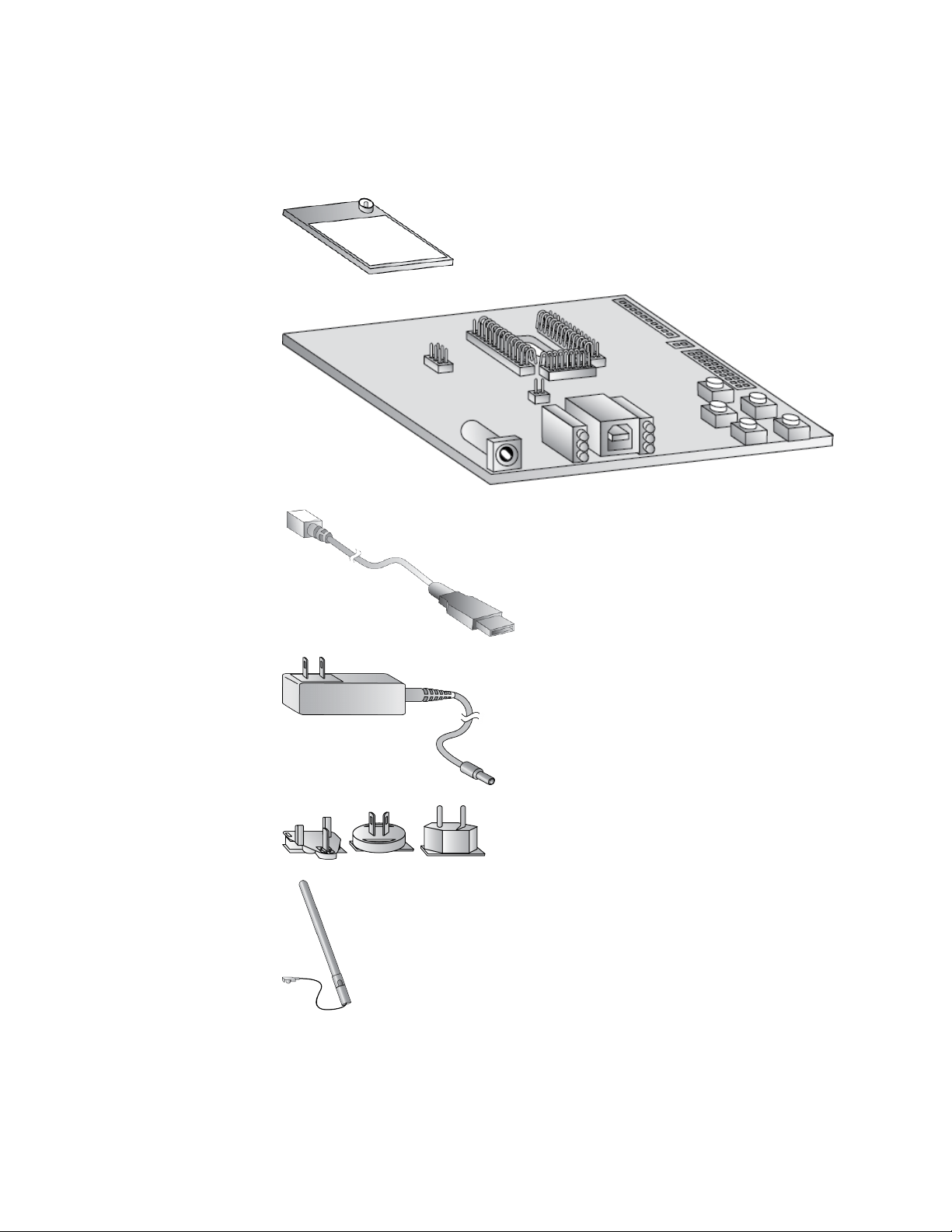
The XBee SX 868 RF Module development kit contains the following components:
XBee
U.FLmodule (3)
XBee
development
board (3)
USB cable (2)
Power supply
(2)
Set of power
supply adapters
(2)
Antenna U.FL
(3)
XBee® SX 868 RF Module User Guide
22
Page 23
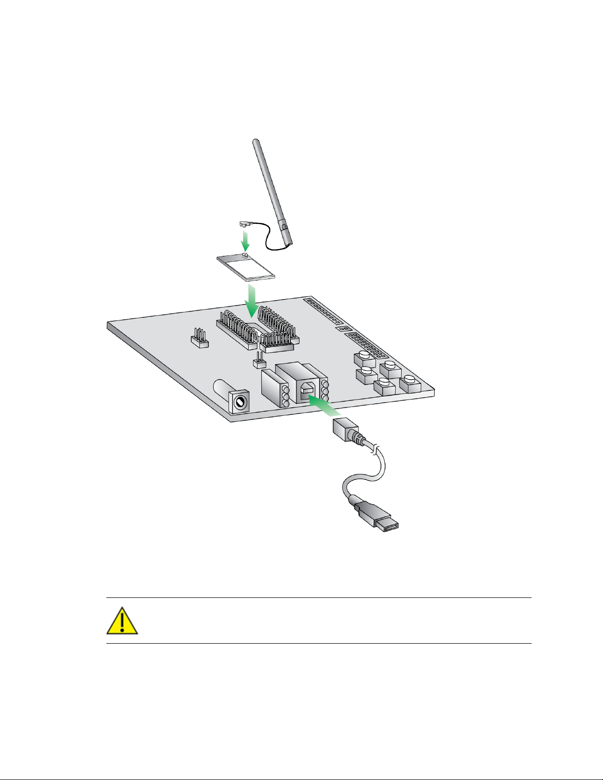
Get started Connect the hardware
Connect the hardware
The following illustration shows you how to assemble the hardware components of the development
kit.
1. Attach the XBee SX 868 RF Modules to the development boards.
2. Attach the antennas to the devices.
3. Connect the USB cables to the development boards.
CAUTION! Before you remove a device from a development board, make sure the board is
not powered by a USB cable or a battery.
XBee® SX 868 RF Module User Guide
23
Page 24

Get started Configure the device using XCTU
Configure the device using XCTU
XBee Configuration and Test Utility (XCTU) is a multi-platform program that enables users to interact
with Digi radio frequency (RF) devices through a graphical interface. The application includes built-in
tools that make it easy to set up, configure, and test Digi RF devices.
For instructions on downloading and using XCTU, see the XCTU User Guide.
Click Discover devices and follow the instructions. XCTU should discover the connected XBee SX 868
RF Modules using the provided settings.
Click Add selected devices.The devices appear in the Radio Modules list. You can click a module to
view and configure its individual settings. For more information on these items, see AT commands.
Configure the devices for a range test
For devices to communicate with each other, you must configure them so they are in the same
network. To obtain all possible data from the remote device, you must also set the local device to API
mode. For more information on API mode, see Operate in API mode.
For devices to communicate with each other, you configure them so they are in the same network.
You also set the local device to API mode to obtain all possible data of the remote device.
When you connect the development board to a PC for the first time, the PC automatically installs
drivers, which may take a few minutes to complete.
1. Add the two devices to XCTU.
2. Select the first module and click the Load default firmware settings button.
3. Configure the following parameters:
ID: 2015
NI: LOCAL_DEVICE
AP: API Mode Without Escapes [1]
4. Click the Write radio settings button.
5. Select the other module and click the Default firmware settings button.
6. Configure the following parameters:
ID: 2015
NI: REMOTE_DEVICE
AP: Transparent Mode [0]
7. Click the Write radio settings button.
After you write the radio settings for each device, their names appear in the Radio Modules
area. The Port indicates that the LOCAL_DEVICE is in API mode.
8. Disconnect REMOTE_DEVICE from the computer, remove it from XCTU, and connect it to its
own power supply.
9. Leave LOCAL_DEVICE connected to the computer. Connect LOCAL_DEVICE to its own power
supply.
10. Place REMOTE_DEVICE at the testing location and connect its power supply.
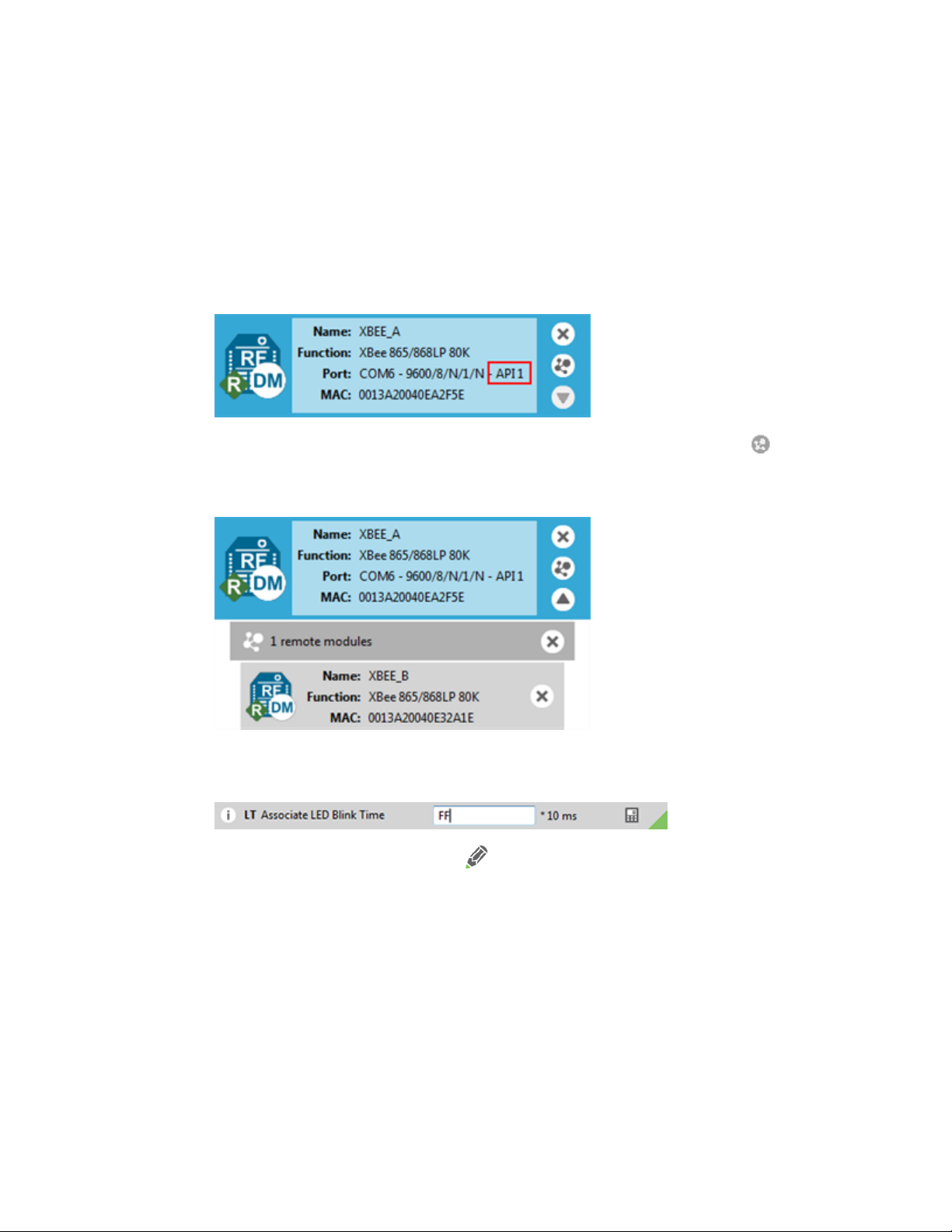
Configure remote devices
You can communicate with remote devices over the air through a corresponding local device.
Configure the local device in API mode because remote commands only work in API mode. Configure
remote devices in either API or Transparent mode.
XBee® SX 868 RF Module User Guide
24
Page 25
Get started Configure remote devices
These instructions show you how to configure the LT (Associated LED Blink Time) parameter on a
remote device.
1. Add two XBee devices to XCTU.
2. Configure the first device in APImode and name it XBEE_A.
3. Configure the second device in either API or Transparent mode, and name it XBEE_B.
4. Disconnect XBEE_B from your computer and remove it from XCTU.
5. Connect XBEE_B to a power supply (or laptop or portable battery).
The Radio Modules area should look something like this.
6.
Select XBEE_A and click the Discover radio nodes in the same network button .
7. Click Add selected devices in the Discovering remote devices dialog. The discovered remote
device appears below XBEE_A.
8. Select the remote device XBEE_B, and configure the following parameter:
LT: FF (hexidecimal representation for 2550 ms)
9.
Click the Write radio settings button .
The remote XBee device now has a different LED blink time.
10. To return to the default LED blink times, change the LT parameter back to 0 for XBEE_B.
XBee® SX 868 RF Module User Guide
25
Page 26
Get started Perform a range test
Perform a range test
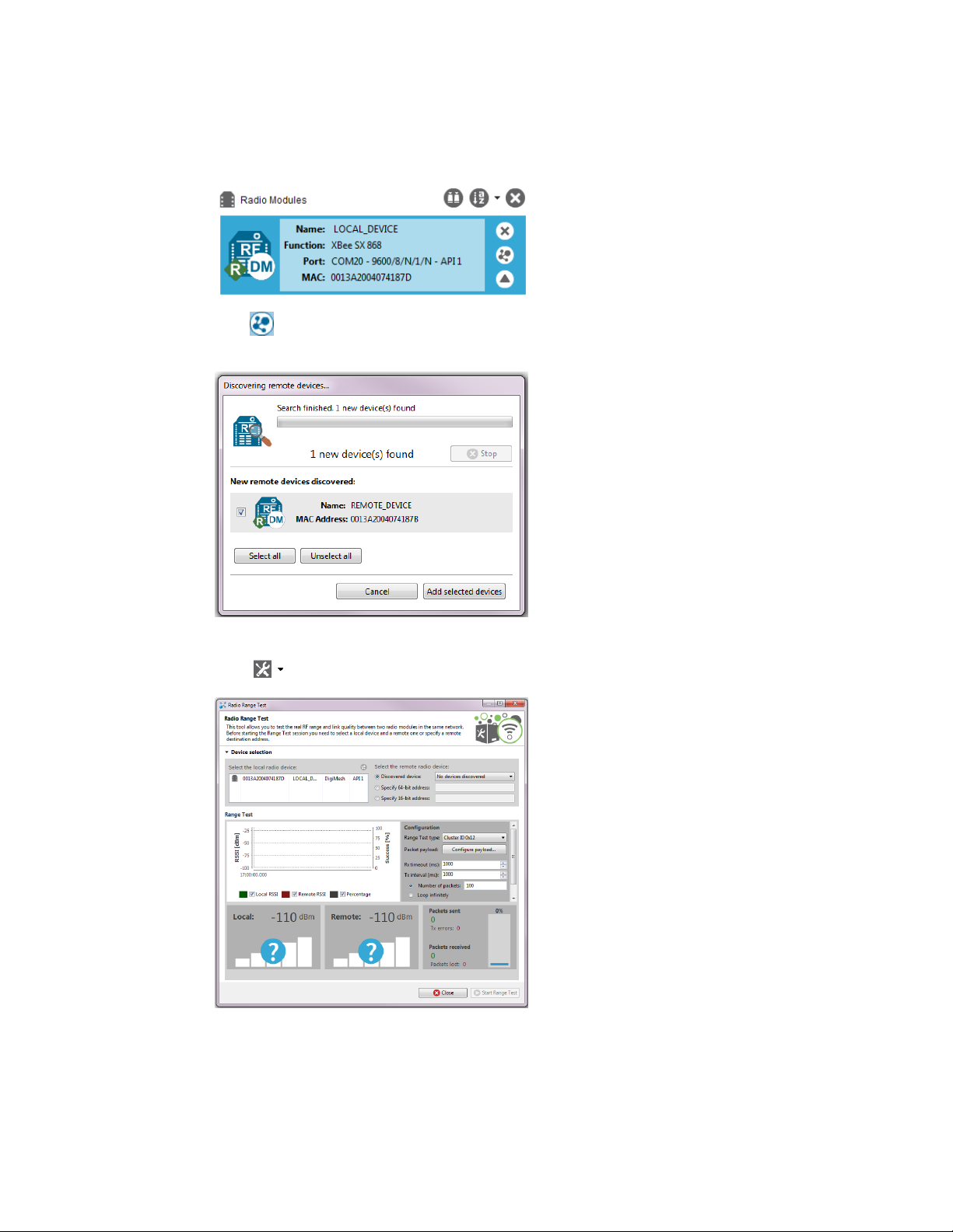
1. Go to the XCTU display for LOCAL_DEVICE.
2.
Click to discover remote devices within the same network. The Discover remote devices
dialog appears.
3. Click Add selected devices.
4.
Click and select Range test. The Radio Range Test dialog appears.
5. In the Select the local radio device area, select LOCAL_DEVICE. XCTU automatically selects
the Discovered device radio button and enables the Start Range Test button.
XBee® SX 868 RF Module User Guide
26
Page 27
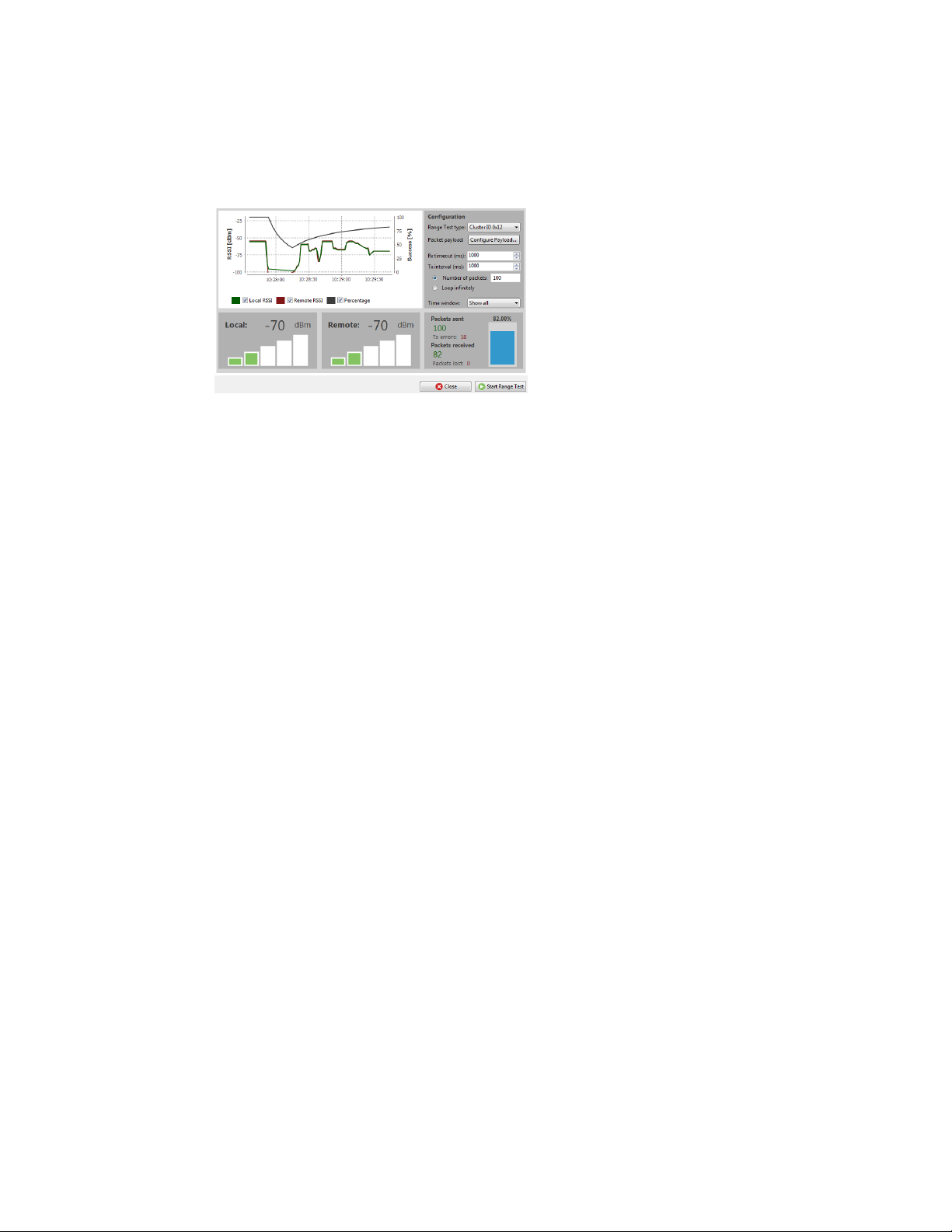
Get started XBee Network Assistant
6. Click Start Range Test to begin the range test.
If the test is running properly, the packets sent should match the packets received. You will
also see the received signal strength indicator (RSSI) update for each radio after each
reception.
7. You can move the LOCAL_DEVICE and REMOTE_DEVICE farther from each other to observe the
signal strength at different distances.
8. Click Stop Range Test when the test is complete.
9. You can test different data rates by reconfiguring the BR (RF Data Rate) parameters on both
devices and starting a new range test.
XBee Network Assistant
The XBee Network Assistant is an application designed to inspect and manage RF networks created
by Digi XBee devices. Features include:
n Join and inspect any nearby XBee network to get detailed information about all the nodes it
contains.
n Update the configuration of all the nodes of the network, specific groups, or single devices
based on configuration profiles.
n Geo-locate your network devices or place them in custom maps and get information about the
connections between them.
n Export the network you are inspecting and import it later to continue working or work offline.
n Use automatic application updates to keep you up to date with the latest version of the tool.
See the XBee Network Assistant User Guide for more information.
To install the XBee Network Assistant:
1. Navigate to digi.com/xbeenetworkassistant.
2. Click General Diagnostics, Utilities and MIBs.
3. Click the XBee Network Assistant - Windows x86 link.
4. When the file finishes downloading, run the executable file and follow the steps in the XBee
Network Assistant Setup Wizard.
XBee Multi Programmer
The XBee Multi Programmer is a combination of hardware and software that enables partners and
distributors to program multiple Digi Radio frequency (RF) devices simultaneously. It provides a fast
and easy way to prepare devices for distribution or large networks deployment.
XBee® SX 868 RF Module User Guide
27
Page 28

Get started XBee Multi Programmer
The XBee Multi Programmer board is an enclosed hardware component that allows you to program up
to six RF modules thanks to its six external XBee sockets. The XBee Multi Programmer application
communicates with the boards and allows you to set up and execute programming sessions. Some of
the features include:
n Each XBee Multi Programmer board allows you to program up to six devices simultaneously.
Connect more boards to increase the programming concurrency.
n Different board variants cover all the XBee form factors to program almost any Digi RF device.
Download the XBee Multi Programmer application from:digi.com/support/productdetail?pid=5641
See the XBee Multi Programmer User Guide for more information.
XBee® SX 868 RF Module User Guide
28
Page 29

Hardware
Mechanical drawings 30
Pin signals 31
XBee® SX 868 RF Module User Guide
29
Page 30

Hardware Mechanical drawings
Mechanical drawings
The following figures show the XBee SX 868 RF Module mechanical drawings. All dimensions are in
centimeters. The XBee SX 868 RF Module differs from other surface-mount XBee modules. It has an
additional ground pad on the underside of the module used for heat dissipation. For more details, see
PCB design and manufacturing.
XBee® SX 868 RF Module User Guide
30
Page 31

Hardware Pin signals
Pin signals
The following table describes the pin signals. Low-asserted signals are distinguished with a horizontal
line over the signal name.
Pin Name I/O
1 GND - - Ground
2 VCC I - Power supply
3 DOUT I/O Output UART data out
4
5 DIO12 I/O Disabled GPIO
XBee® SX 868 RF Module User Guide
DIN/CONFIG
Default
state Function
I/O Input UART data in
31
Page 32

Hardware Pin signals
Default
Pin Name I/O
state Function
6
RESET
I - Drive low to reset device. Do not drive pin high; pin
may only be driven open drain or low. Pin has an
internal 20k pullup resistor. The minimum reset
pulse time is 100 ns.
7 DIO10/RSSI/PWM0 I/O Output GPIO / RX Signal Strength Indicator
8 DIO11/PWM1 I/O Disabled GPIO / Pulse Width Modulator
9 [Reserved] - - Do not connect
10
DIO8/DTR /SLEEP_
RQ
I/O Input
GPIO / Pin Sleep Control line (DTR on the
development board)
11 GND - - Ground
12
DO19/SPI_ATTN
O Output GPO / Serial Peripheral Interface (SPI)Attention or
UART Data Present indicator
13 GND - - Ground
14 DO18/SPI_CLK I/O1Input GPO / SPI clock
15
DO17/SPI_SSEL
I/O2Input GPO / SPI not select
16 DO16/SPI_MOSI I/O3Input GPO / SPI Data In
17 DO15/SPI_MISO O Output
GPO/SPI Data Out Tri-stated when SPI_SSEL is
high
18 [Reserved] - - Do not connect
19 [Reserved] - - Do not connect
20 [Reserved] - - Do not connect
21 [Reserved] - - Do not connect
22 GND - - Ground
23 [Reserved] - - Do not connect
24 DIO4 I/O Disabled GPIO
25
26
1
Pins 14-16 are inputs in SPI mode only. In general purpose I/O pin mode you can only use them as digital
outputs.
2
Pins 14-16 are inputs in SPI mode only. In general purpose I/O pin mode you can only use them as digital
outputs.
3
Pins 14-16 are inputs in SPI mode only. In general purpose I/O pin mode you can only use them as digital
outputs.
DIO7/CTS
DIO9/ON/SLEEP
I/O Output GPIO / UART Clear to Send Flow Control
I/O Output GPIO / Module Sleep Status Indicator
XBee® SX 868 RF Module User Guide
32
Page 33

Hardware Pin signals
Default
Pin Name I/O
state Function
27
28 DIO5/ASSOC I/O Output GPIO / Associate Indicator
29
30 DIO3/AD3 I/O Disabled GPIO / Analog Input
31 DIO2/AD2 I/O Disabled GPIO / Analog Input
32 DIO1/AD1 I/O Disabled GPIO / Analog Input
33 DIO0/AD0 I/O Input GPIO / Analog Input / Commissioning Pushbutton
34 [Reserved] - - Do not connect
35 GND - - Ground
36 RF_PAD I/O - RF connection for RF pad variant
37 [Reserved] - - Do not connect
38 GND - - Ground pad for heat transfer to host PCB. Located
V
REF
DIO6/RTS
- - Feature not supported on this device. Used on
other XBee devices for analog voltage reference.
I/O Disabled GPIO / UART Request to Send Flow Control
on the underside of the XBee module.
Pin connection recommendations
The only required pin connections are VCC, GND, DOUT and DIN. To support serial firmware updates,
you should connect VCC, GND, DOUT, DIN, RTS, and SLEEP (DTR).
XBee® SX 868 RF Module User Guide
33
Page 34

Operation
Operation 35
Listen Before Talk and Automatic Frequency Agility 35
Single frequency mode band mode 36
Serial communications 36
Configuration considerations 40
Serial buffers 41
UART flow control 41
Serial interface protocols 42
XBee® SX 868 RF Module User Guide
34
Page 35

Operation Operation
Operation
The XBee SX 868 RF Module uses a multi-layered firmware base to order the flow of data, dependent
on the hardware and software configuration you choose. The following configuration block diagram
shows the host serial interface as the physical starting point and the antenna as the physical endpoint
for the transferred data. A block must be able to touch another block above or below it for the two
interfaces to interact. For example, if the device uses SPI mode, Transparent mode is not available as
shown in the following image:
The command handler code processes commands from AT Command Mode or API Mode; see API serial
exchanges. The command handler also processes commands from remote devices; see Remote AT
commands.
Listen Before Talk and Automatic Frequency Agility
This device implements Listen Before Talk (LBT) and Automatic Frequency Agility (AFA). The advantage
of LBT with AFA is that the device bypasses the Duty Cycle requirement imposed by European
standards. LBT+AFA requires that you use at least two frequencies for transmission. See Regulatory
conformity summary for a complete list of channels and frequencies.
This feature provides a level of fairness to the devices in a given area. Before this device transmits, it
senses a channel to determine if there is activity by taking an RSSI measurement for 5 ms. If the
measurement is below the threshold, the device transmits on that channel. If there is activity, that
channel is not used, and the device listens for at least 5 ms to allow transmissions to be received.
After the device transmits on a channel, it will not transmit on that channel again until the minimum
TX off time has been met, which is greater than 100 ms. It is useful to have many channels in your
channel mask, so transmissions are less likely to be delayed.
European requirements also state that only 100 seconds of transmission may occur over the period of
an hour on 200 kHz of spectrum. This method simplifies and optimizes the calculations of spectrum
use over the period of one hour. The standard states that the more channels you have, the more
XBee® SX 868 RF Module User Guide
35
Page 36

Operation Single frequency mode band mode
transmission time you have in a one hour period. Calculate the effective duty cycle based on the
number of available channels enabled as follows:
Effective Duty Cycle = (number of channels * 100)/3600.
For example, if you enabled two channels you would have an effective duty cycle of 5.6%.
The XBee SX 868 RF Module uses a sliding bucket algorithm to calculate usage over the period of 1
hour for each channel. Each bucket accumulates for 6 minutes.
This device has a maximum of 28 AFA channels to choose from, and channels can be excluded by
setting the channel mask (CM) to reduce them. Since not all countries allow for all of these channels,
the set may be dramatically smaller for some countries. For a complete list, refer to www.digi.com.
Single frequency mode band mode
When you set the channel mask to 0x20000000, the device is in a single frequency mode, and the
frequency is 869.85 MHz. In this mode:
n LBT+AFA mode is disabled.
n The device assumes no duty cycle requirement (or 100% duty cycle).
n The PL is automatically limited to 5 mW to comply with the single frequency mode
requirements.
Serial communications
RF Modules interface to a host device through a serial port. Using its serial port, the device
communicates with any of the following:
n Logic and voltage compatible UART
n Level translator to any serial device (for example, through an RS-232 or USB interface board)
UART data flow
Devices that have a UART interface connect directly to the pins of the XBee SX 868 RF Module as
shown in the following figure. The figure shows system data flow in a UART-interfaced environment.
Low-asserted signals have a horizontal line over the signal name.
Serial data
A device sends data to the XBee SX 868 RF Module's UART through pin 4 DIN as an asynchronous serial
signal. When the device is not transmitting data, the signals should idle high.
XBee® SX 868 RF Module User Guide
36
Page 37

Operation Serial communications
For serial communication to occur, you must configure the UART of both devices (the microcontroller
and the XBee SX 868 RF Module) with compatible settings for the baud rate, parity, start bits, stop
bits, and data bits.
Each data byte consists of a start bit (low), 8 data bits (least significant bit first) and a stop bit (high).
The following diagram illustrates the serial bit pattern of data passing through the device. The
diagram shows UART data packet 0x1F (decimal number 31) as transmitted through the device.
SPI communications
The XBee SX 868 RF Module supports SPI communications in slave mode. Slave mode receives the
clock signal and data from the master and returns data to the master. The following table shows the
signals that the SPI port uses on the device.
Signal Function
SPI_MOSI
Inputs serial data from the master
(MasterOut,SlaveIn)
SPI_MISO(Master
Outputs serial data to the master
In,Slave Out)
SPI_SCLK(SerialClock)
SPI_SSEL (SlaveSelect)
Clocks data transfers on MOSI and MISO
Enables serial communication with the slave
SPI_ATTN (Attention) Alerts the master that slave has data queued to send. The XBee SX 868 RF
Module asserts this pin as soon as data is available to send to the SPI
master and it remains asserted until the SPI master has clocked out all
available data.
In this mode:
n Data is most significant bit (MSB) first.
n Frame Format mode 0 is used. This means CPOL= 0 (idle clock is low) and CPHA = 0 (data is
sampled on the clock’s leading edge).
n The SPI port only supports API Mode (AP = 1).
The following diagram shows the frame format mode 0 for SPI communications.
XBee® SX 868 RF Module User Guide
37
Page 38

Operation Serial communications
SPI operation
This section specifies how SPI is implemented on the device, what the SPI signals are, and how full
duplex operations work.
SPI implementation
The XBee SX 868 RF Module operates as a SPI slave only. This means an external master provides the
clock and decides when to send data. The XBee SX 868 RF Module supports an external clock rate of
up to 6 Mhz (6 Mb/s).
The device transmits and receives data with the most significant bit first using SPI mode 0. This
means the CPOL and CPHA are both 0. We chose Mode 0 because it is the typical default for most
microcontrollers and simplifies configuring the master.
SPI signals
The XBee SX 868 RF Module supports SPI communications in slave mode. Slave mode receives the
clock signal and data from the master and returns data to the master. The SPI port uses the following
signals on the device:
Signal Pin number Applicable AT command
SPI_MOSI (Master out, Slave in)
SPI_MISO (Master in, Slave out)
SPI_SCLK (Serial clock)
SPI_SSEL (Slave select)
SPI_ATTN (Attention)
By default, the inputs have pull-up resistors enabled. Use the PR command to disable the pull-up
resistors. When the SPI pins are not connected but the pins are configured for SPI operation, then the
device requires the pull-ups for proper UART operation.
Signal description
SPI_MISO: When SPI_SSEL is asserted (low) and SPI_CLK is active, the device outputs the data on this
line at the SPI_CLK rate. When SPI_SSEL is de-asserted (high), you should tri-state this output such
that another slave device can drive the line.
17
16
15
14
12
P5
P6
P7
P8
P9
XBee® SX 868 RF Module User Guide
38
Page 39

Operation Serial communications
SPI_MOSI:The SPI master outputs data on this line at the SPI_CLK rate after it selects the desired
slave. When you configure the device for SPI operations, this pin is an input.
SPI_SCLK: The SPI master outputs a clock on this pin, and the rate must not exceed the maximum
allowed, 6 Mb/s. When you configure the device for SPI operations, this pin is an input. Thissignal
enables serial communication with the slave.
SPI_SSEL:The SPI master outputs a low signal on this line to select the desired slave. When you
configure the device for SPI operations, this pin is an input. Thissignal clocks data transfers on MOSI
and MISO.
SPI_ATTN: The device asserts this pin low when it has data to send to the SPI master. When you
configure this pin for SPI operations, it is an output (not tri-stated). This signal alerts the master that
the slave has data queued to send. The device asserts this pin as soon as data is available to send to
the SPI master and it remains asserted until the SPI master has clocked out all available data.
Full duplex operation
SPI on the XBee SX 868 RF Module requires that you use API mode (without escaping) to packetize
data. By design, SPI is a full duplex protocol even when data is only available in one direction. This
means that when a device receives data, it also transmits and that data is normally invalid. Likewise,
when the device transmits data, invalid data is probably received. To determine whether or not
received data is invalid, we packetize the data with API packets.
SPI allows for valid data from the slave to begin before, at the same time, or after valid data begins
from the master. When the master is sending data to the slave and the slave has valid data to send in
the middle of receiving data from the master, this allows a true full duplex operation where data is
valid in both directions for a period of time. Not only must the master and the slave both be able to
keep up with the full duplex operation, but both sides must honor the protocol as specified.
The following diagram illustrates the SPI interface while valid data is being sent in both directions.
Low power operation
Sleep modes generally work the same on SPI as they do on UART. However, due to the addition of SPI
mode, there is an option of another sleep pin, as described below.
By default, Digi configures DIO8 (SLEEP_REQUEST) as a peripheral and during pin sleep it wakes the
device and puts it to sleep. This applies to both the UART and SPI serial interfaces.
If SLEEP_REQUEST is not configured as a peripheral and SPI_SSEL is configured as a peripheral, then
pin sleep is controlled by SPI_SSEL rather than by SLEEP_REQUEST. Asserting SPI_SSEL (pin 15) by
driving it low either wakes the device or keeps it awake. Negating SPI_SSEL by driving it high puts the
device to sleep.
Using SPI_SSEL to control sleep and to indicate that the SPI master has selected a particular slave
device has the advantage of requiring one less physical pin connection to implement pin sleep on SPI.
XBee® SX 868 RF Module User Guide
39
Page 40

Operation Configuration considerations
It has the disadvantage of putting the device to sleep whenever the SPI master negates SPI_SSEL
(meaning time is lost waiting for the device to wake), even if that was not the intent.
If the user has full control of SPI_SSEL so that it can control pin sleep, whether or not data needs to be
transmitted, then sharing the pin may be a good option in order to make the SLEEP_REQUEST pin
available for another purpose.
If the device is one of multiple slaves on the SPI, then the device sleeps while the SPI master talks to
the other slave, but this is acceptable in most cases.
If you do not configure either pin as a peripheral, then the device stays awake, being unable to sleep in
SM1 mode.
Configuration considerations
The configuration considerations are:
n How do you select the serial port? For example, should you use the UART or the SPI port?
n If you use the SPI port, what data format should you use in order to avoid processing invalid
characters while transmitting?
n What SPI options do you need to configure?
Serial port selection
In the default configuration both the UART and SPI ports are configured for serial port operation. In
this case, serial data goes out the UART until the host device asserts the SPI_SSEL signal. Thereafter
all serial communications operate only on the SPI interface until a reset occurs.
If you enable only the UART, the XBee SX 868 RF Module uses only the UART, and ignores the SPI_
SSEL.
If you enable only the SPI, the XBee SX 868 RF Module uses only the SPI, and ignores UART
communications.
Data format
SPI only operates in API mode 1. The XBee SX 868 RF Module does not support Transparent mode or
API mode 2 (which escapes control characters). This means that the AP configuration only applies to
the UART, and the device ignores it while using SPI.
SPI parameters
Most host processors with SPI hardware allow you to set the bit order, clock phase and polarity. For
communication with all XBee SX 868 RF Modules, the host processor must set these options as
follows:
n Bit order: send MSB first
n Clock phase (CPHA):sample data on first (leading) edge
n Clock polarity (CPOL): first (leading) edge rises
All XBee SX 868 RF Modules use SPI mode 0 and MSB first. Mode 0 means that data is sampled on the
leading edge and that the leading edge rises. MSB first means that bit 7 is the first bit of a byte sent
over the interface.
XBee® SX 868 RF Module User Guide
40
Page 41

Operation Serial buffers
Serial buffers
To enable the UART port, DIN and DOUT must be configured as peripherals. To enable the SPI port,
SPI_MISO, SPI_MOSI, SPI_SSEL, and SPI_CLK must be enabled as peripherals. If both ports are
enabled, output goes to the UART until the first input on SPI. This is the default configuration.
When input occurs on either port, that port is selected as the active port and no input or output is
allowed on the other port until the next reset of the module.
If you change the configuration to configure only one port, that port is the only one enabled or used. If
the parameters are written with only one port enabled, the port that is not enabled is not used even
temporarily after the next reset.
If both ports are disabled on reset, the device uses the UART regardless of the incorrect configuration
to ensure that at least one serial port is operational.
Serial receive buffer
When serial data enters the device through the DIN pin (or the MOSI pin), it stores the data in the
serial receive buffer until the device can process it. Under certain conditions, the device may not be
able to process data in the serial receive buffer immediately. If large amounts of serial data are sent
to the device such that the serial receive buffer would overflow, then it discards new data. If the UART
is in use, you can avoid this by the host side honoring CTS flow control.
If the SPI is the serial port, no hardware flow control is available. It is your responsibility to ensure
that the receive buffer does not overflow. One reliable strategy is to wait for a TX_STATUS response
after each frame sent to ensure that the device has had time to process it.
Serial transmit buffer
When the device receives RF data, it moves the data into the serial transmit buffer and sends it out
the UART or SPI port. If the serial transmit buffer becomes full and the system buffers are also full,
then it drops the entire RF data packet. Whenever the device receives data faster than it can process
and transmit the data out the serial port, there is a potential of dropping data.
UART flow control
You can use the RTS and CTS pins to provide RTS and/or CTS flow control. CTS flow control provides an
indication to the host to stop sending serial data to the device. RTS flow control allows the host to
signal the device to not send data in the serial transmit buffer out the UART. To enable RTS/CTS flow
control, use the D6 and D7 commands.
Note Serial port flow control is not possible when using the SPI port.
CTS flow control
If you enable CTS flow control (D7 command), when the serial receive buffer is 17 bytes away from
being full, the device de-asserts CTS (sets it high) to signal to the host device to stop sending serial
data. The device reasserts CTS after the serial receive buffer has 34 bytes of space. See FT (Flow
Control Threshold) for the buffer size.
In either case, CTS is not re-asserted until the serial receive buffer has FT-17 or less bytes in use.
XBee® SX 868 RF Module User Guide
41
Page 42

Operation Serial interface protocols
RTS flow control
If you send the D6 command to enable RTS flow control, the device does not send data in the serial
transmit buffer out the DOUT pin as long as RTS is de-asserted (set high). Do not de-assert RTS for
long periods of time or the serial transmit buffer will fill. If the device receives an RF data packet and
the serial transmit buffer does not have enough space for all of the data bytes, it discards the entire
RF data packet.
The UART Data Present Indicator is a useful feature when using RTS flow control. When enabled, the
DIO19 line asserts (low asserted) when UART data is queued to be transmitted from the device. For
more information, see P9 (DIO19/SPI_ATTN).
If the device sends data out the UART when RTS is de-asserted (set high) the device could send up to
five characters out the UART port after RTS is de-asserted.
Serial interface protocols
The XBee SX 868 RF Module supports both Transparent and Application Programming Interface (API)
serial interfaces.
Transparent operating mode
When operating in Transparent mode, the devices act as a serial line replacement. The device queues
up all UART data received through the DIN pin for RF transmission. When RF data is received, the
device sends the data out through the serial port. Use the Command mode interface to configure the
device configuration parameters.
Note Transparent operation is not provided when using SPI.
The device buffers data in the serial receive buffer and packetizes and transmits the data when it
receives the following:
n No serial characters for the amount of time determined by the RO (Packetization Timeout)
parameter. If RO = 0, packetization begins when the device received a character.
n Command Mode Sequence (GT + CC + GT). Any character buffered in the serial receive buffer
before the device transmits the sequence.
n Maximum number of characters that fit in an RF packet.
API operating mode
API operating mode is an alternative to Transparent operating mode. The frame-based API extends
the level to which a host application can interact with the networking capabilities of the device. When
in API mode, the device contains all data entering and leaving in frames that define operations or
events within the device.
The API provides alternative means of configuring devices and routing data at the host application
layer. A host application can send data frames to the device that contain address and payload
information instead of using Command mode to modify addresses. The device sends data frames to
the application containing status packets, as well as source and payload information from received
data packets.
The API operation option facilitates many operations such as:
XBee® SX 868 RF Module User Guide
42
Page 43

Operation Serial interface protocols
n Transmitting data to multiple destinations without entering Command Mode
n Receive success/failure status of each transmitted RF packet
n Identify the source address of each received packet
XBee® SX 868 RF Module User Guide
43
Page 44

Advanced application features
Remote configuration commands 45
Network commissioning and diagnostics 45
I/O line monitoring 54
I/O line passing 58
General Purpose Flash Memory 60
Over-the-air firmware updates 67
Software libraries 69
XBee® SX 868 RF Module User Guide
44
Page 45

Advanced application features Remote configuration commands
Remote configuration commands
The API firmware has provisions to send configuration commands to remote devices using the
Remote Command Request API frame (see Operate in API mode). Use the APIframe to send
commands to a remote device to read or set command parameters.
Send a remote command
To send a remote command, populate the Remote Command Request frame with:
n 64-bit address of the remote device
n Correct command options value
n Command and parameter data (optional)
If you want a command response, set the Frame ID set to a non-zero value. Only unicasts of remote
commands are supported, and remote commands cannot be broadcast.
Apply changes on remote devices
When you use remote commands to change command parameter settings on a remote device,
parameter changes do not take effect until you apply the changes. For example, changing the BD
parameter does not change the serial interface on the remote until the changes are applied. To apply
changes, do one of the following:
n Set the apply changes option bit in the API frame.
n Issue an AC (Apply Changes) command to the remote device.
n Issue a WR + FR command to the remote device to save changes and reset the device.
Remote command responses
If the remote device receives a remote command request transmission, and the API frame ID is nonzero, the remote sends a remote command response transmission back to the device that sent the
remote command. When a remote command response transmission is received, a device sends a
remote command response API frame out its serial port. The remote command response indicates
the status of the command (success, or reason for failure), and in the case of a command query, it
includes the register value. The device that sends a remote command will not receive a remote
command response frame if either of the following conditions exist:
n The destination device could not be reached.
n The frame ID in the remote command request is set to 0.
Network commissioning and diagnostics
We call the process of discovering and configuring devices in a network for operation, "network
commissioning." Devices include several device discovery and configuration features. In addition to
configuring devices, you must develop a strategy to place devices to ensure reliable routes. To
accommodate these requirements, modules include features to aid in placing devices, configuring
devices, and network diagnostics.
XBee® SX 868 RF Module User Guide
45
Page 46

Advanced application features Network commissioning and diagnostics
Configure devices
You can configure XBee devices locally through serial commands (AT or API) or remotely through
remote API commands. API devices can send configuration commands to set or read the configuration
settings of any device in the network.
Network link establishment and maintenance
Build aggregate routes
In many applications it is necessary for many or all of the nodes in the network to transmit data to a
central aggregator node. In a new DigiMesh network the overhead of these nodes discovering routes
to the aggregator node can be extensive and taxing on the network. To eliminate this overhead, use
the AG command to automatically build routes to an aggregate node in a DigiMesh network.
Send a unicast
To send a unicast, devices configured for Transparent mode (AP = 0) must set their DH/DL registers to
the MAC address of the node which they need to transmit to. In networks of Transparent mode
devices which transmit to an aggregator node, it is necessary to set every device's DH/DL registers to
the MAC address of the aggregator node. Use the AG command to set the DH/DL registers of all the
nodes in a DigiMesh network to that of the aggregator node.
Use the AG command
Upon deploying a DigiMesh network, send the AG command on the desired aggregator node to cause
all nodes in the network to build routes to the aggregator node. You can use the command to
automatically update the DH/DL registers to match the MAC address of the aggregator node.
The AG command requires a 64-bit parameter. The parameter indicates the current value of the
DH/DL registers on a device which should be replaced by the 64-bit address of the node sending the
AG broadcast. If it is not desirable to update the DH/DL of the device receiving the AG broadcast, you
can use the invalid address of 0xFFFE. API enabled devices output an Aggregate Addressing Update-
0x8E if they update their DH/DL address.
All devices that receive an AG broadcast update their routing table information to build a route to the
sending device, regardless of whether or not their DH/DL address is updated. This routing information
will be used for future transmissions of DigiMesh unicasts.
Example 1: To update the DH/DL registers of all modules in the network to be equal to the MAC
address of an aggregator node with a MAC address of 0x0013a2004052c507 after network
deployment the following technique could be employed:
1. Deploy all devices in the network with the default DH/DL of 0xFFFF.
2. Send an ATAGFFFF command on the aggregator node.
Following the preceding sequence would result in all of the nodes in the network which received the
AG broadcast to have a DH of 0x0013a200 and a DL of 0x4052c507. These nodes would have
automatically built a route to the aggregator.
Example 2: To cause all nodes in the network to build routes to an aggregator node with a MAC
address of 0x0013a2004052c507 without affecting the DH/DL of any nodes in the network, send the
AGFFFE command on the aggregator node. This sends an AG broadcast to all nodes in the network.
All of the nodes will update their internal routing table information to contain a route to the
aggregator node. None of the nodes update their DH/DL registers, because none of the registers are
set to an address of 0xFFFE.
XBee® SX 868 RF Module User Guide
46
Page 47

Advanced application features Network commissioning and diagnostics
Node replacement
You can also use the AG command to update the routing table and DH/DL registers in the network
after a device is replaced, and you can update the DH/DL registers of nodes in the network.
n To update only the routing table information without affecting the DH/DL registers, use
Example 2.
n To update the DH/DL registers of the network, use the method in the following example.
Example: Use the device with serial number 0x0013a2004052c507 as a network aggregator and
replace it with a device with serial number 0x0013a200f5e4d3b2. Issue the AG0013a2004052c507
command on the new module. This causes all devices with a DH/DL register setting of
0x0013a2004052c507 to update their DH/DL register setting to the MAC address of the sending
device (0x0013a200f5e4d3b2).
Place devices
For a network installation to be successful, installers must be able to determine where to place
individual XBee devices to establish reliable links throughout the network.
RSSI indicators
It is possible to measure the received signal strength on a device using the DB command. DB returns
the RSSI value (measured in -dBm) of the last received packet. However, this number can be
misleading in DigiMesh networks. The DB value only indicates the received signal strength of the last
hop. If a transmission spans multiple hops, the DB value provides no indication of the overall
transmission path, or the quality of the worst link; it only indicates the quality of the last link.
Determine the DB value in hardware using the RSSI/PWM device pin (pin 7). If you enable the RSSI
PWM functionality (P0 command), when the device receives data, it sets the RSSI PWM to a value
based on the RSSI of the received packet (this value only indicates the quality of the last hop). You
could connect this pin to an LED to indicate if the link is stable or not.
Test links in a network - loopback cluster
To measure the performance of a network, you can send unicast data through the network from one
device to another to determine the success rate of several transmissions. To simplify link testing, the
devices support a Loopback cluster ID (0x12) on the data endpoint (0xE8). The cluster ID on the data
endpoint sends any data transmitted to it back to the sender.
The following figure demonstrates how you can use the Loopback cluster ID and data endpoint to
measure the link quality in a mesh network.
XBee® SX 868 RF Module User Guide
47
Page 48

Advanced application features Network commissioning and diagnostics
The configuration steps for sending data to the loopback cluster ID depend on what mode the device
is in. For details on setting the mode, see AP (API Mode). The following sections list the steps based on
the device's mode.
Transparent operating mode configuration (AP = 0)
To send data to the loopback cluster ID on the data endpoint of a remote device:
1. Set the CI command to 0x12.
2. Set the SE and DE commands to 0xE8 (default value).
3. Set the DH and DL commands to the address of the remote (0 for the coordinator, or the 64-bit
address of the remote).
After exiting Command mode, the device transmits any serial characters it received to the remote
device, which returns those characters to the sending device.
API operating mode configuration (AP = 1 or AP = 2)
Send an Explicit Addressing Command Request - 0x11 using 0x12 as the cluster ID and 0xE8 as both
the source and destination endpoint.
The remote device echoes back the data packets it receives to the sending device.
Test Link cluster
The primary difference between the Loopback cluster ID (0x12) and the Test Link cluster (0x14) is the
number of hops. With the Loopback cluster you can verify that a route exists across one or more hops
between any two nodes in the network.
With the Test Link cluster you can determine the signal strength between any two nodes without
using intermediate nodes. If the two nodes are too far apart, you can expect 100% failure. If they are
close together, you can expect 100% success.
When placing nodes, the following sequence could occur:
1. You can use the Loopback cluster to verify that a route exists between all nodes of interest; for
example, between the aggregator and each of the other nodes.
2. If step 1 fails, you could perform a trace route on any pair of nodes that failed in step 1. The
trace route indicates the failing link.
3. Once a weak link is identified, you can run Test Link to exercise that link to determine how
strong and reliable it is.
4. Now that the problem has been isolated, you can place nodes apropriately to resolve the
connectivity problems.
Device discovery
Network discovery
Use the network discovery command to discover all devices that have joined a network. Issuing the
ND command sends a broadcast network discovery command throughout the network. All devices
that receive the command send a response that includes:
n Device addressing information
n Node identifier string (see NI (Node Identifier))
n Other relevant information
XBee® SX 868 RF Module User Guide
48
Page 49

Advanced application features Network commissioning and diagnostics
You can use this command for generating a list of all module addresses in a network.
When a device receives the network discovery command, it waits a random time before sending a
response. The device sets the maximum time delay on the ND sender with the NT command. The ND
originator includes its NT setting in the transmission to provide a delay window for all devices in the
network. Large networks may need to increase NT to improve network discovery reliability. The
default NT value is .
Neighbor polling
Use the neighbor poll command to discover the modules which are immediate neighbors (within RF
range) of a particular node. You can use this command to determining network topology and
determining possible routes.
The device sends the command using the FN command. You can initiate the FN command locally on a
node using AT command mode or by using a local AT command request frame. You can also initiate the
command remotely by sending the target node an FN command using a remote AT command request
API frame.
A node that executes an FN command sends a broadcast to all of its immediate neighbors. All devices
that receive this broadcast send an RF packet to the node that initiated the FN command. In an
instance where the device initiates the command remotely, it sends the responses directly to the
node which sent the FN command to the target node. The device outputs the response packet on the
initiating radio in the same format as a network discovery frame.
Link reliability
To install a successful mesh network, you must be able to determine where to place individual XBee
devices to establish reliable links throughout the mesh network.
Network link testing
To determine the success rate of many transmissions, send unicast data through the network from
one device to another to measure the performance of the mesh network.
To simplify link testing, the modules support a loopback cluster ID (0x12) on the data endpoint (0xE8).
The device transmits any data sent to this cluster ID on the data endpoint back to the sender as
illustrated in the following figure:
The configuration steps to send data to the loopback cluster ID depend on the AP setting.
AT configuration (AP=0)
To send data to the loopback cluster ID on the data endpoint of a remote device, set the CI command
value to 0x12. Set the SE and DE commands set to 0xE8 (default value). Set the DH and DL commands
XBee® SX 868 RF Module User Guide
49
Page 50

Advanced application features Network commissioning and diagnostics
to the address of the remote. After exiting command mode, the source device transmits any received
serial characters to the remote device, and returned to the sender.
API configuration (AP=1 or AP=2)
Send an Explicit Addressing Command API frame (0x11) using 0x12 as the cluster ID and 0xE8 as the
source and destination endpoint. The remote device echoes any data packets it receives to the
sender.
Link testing between adjacent devices
To test the quality of a link between two adjacent nodes in a network, use the Test Link Request
Cluster ID send a number of test packets between any two nodes in a network.
Initiate a link test using an Explicit TX Request frame. Address the command frame to the Test Link
Request Cluster ID (0x0014) on destination endpoint 0xE6 on the device to execute the test link. The
Explicit TX Request frame contains a 12 byte payload with the following format:
Number of
bytes Field name Description
8 Destination
address
2 Payload size The size of the test packet. Use the MP command to query the
2 Iterations The number of packets to send. Use a number between 1 and 4000.
After completing the transmissions of the test link packets, the executing device sends the following
data packet to the requesting device's Test Link Result Cluster (0x0094) on endpoint (0xE6). If the
requesting device is operating in API mode, the device outputs the following information as an API
Explicit RX Indicator Frame:
Number of
bytes Field name Description
8 Destination
address
2 Payload size The size of the test packet sent to test the link.
2 Iterations The number of packets sent.
2 Success The number of packets successfully acknowledged.
2 Retries The total number of MAC retries to transfer all the
The address the device tests its link with.
maximum payload size for this device.
The address where the device tested its link.
packets.
1 Result 0x00 - command was successful.
1 RR The maximum number of MAC retries allowed.
1 maxRSSI The strongest RSSI reading observed during the test.
XBee® SX 868 RF Module User Guide
0x03 - invalid parameter used.
50
Page 51

Advanced application features Network commissioning and diagnostics
Number of
bytes Field name Description
1 minRSSI The weakest RSSI reading observed during the test.
1 avgRSSI The average RSSI reading observed during the test.
Example
Suppose that the link between device A (SH/SL = 0x0013a20040521234) and device B
(SH/SL=0x0013a2004052abcd) is being tested by transmitting 1,000 40 byte packets. Send the
following API packet to the serial interface of the device outputting the results, device C. Note that
device C can be the same device as device A or B (Whitespace delineates fields and bold text is the
payload portion of the packet):
7E 0020 11 01 0013A20040521234 FFFE E6 E6 0014 C105 00 00 0013A2004052ABCD 0028 03E8 EB
And the following is a possible packet returned:
7E 0027 91 0013A20040521234 FFFE E6 E6 0094 C105 00 0013A2004052ABCD 0028 03E8 03E7 0064
00 0A 50 53 52 9F
(999 out of 1000 packets successful, 100 retries used, RR=10, maxRSSI= - 80 dBm, minRSSI= - 83 dBm,
avgRSSI= - 82 dBm)
If the result field is not equal to zero then an error occurred. Ignore the other fields in the packet. If
the Success field is equal to zero then ignore the RSSI fields.
Trace routing
Determining the route a DigiMesh unicast takes to its destination is useful when setting up a network
or diagnosing problems within a network. Use the Trace Route API option of Tx Request Packets to
transmit routing information packets to the originator of a DigiMesh unicast by the intermediate
nodes. For a description of the API frames, see API operating mode.
When a unicast is sent with the Trace Route API option enabled, the unicast is sent to its destination
radios which forward the unicast to its eventual destination and transmit a Route Information (RI)
packet back along the route to the unicast originator. For more information, see API operating mode.
Example:
Suppose you unicast a data packet with the trace route enabled from radio A to radio E, through
radios B, C, and D. The following sequence occurs:
n After the successful MAC transmission of the data packet from A to B, A outputs an RI Packet
indicating that the transmission of the data packet from A to E was successfully forwarded one
hop from A to B.
n After the successful MAC transmission of the data packet from B to C, B transmits a RI Packet
to A. Then, A outputs this RI packet out its serial interface.
n After the successful MAC transmission of the data packet from C to D, C transmits a RI Packet
to A (through B). Then, A outputs this RI packet out its serial interface.
n After the successful MAC transmission of the data packet from D to E, D transmits an RI Packet
to A (through C and B). Then, A outputs this RI packet out its serial interface.
Route Information packets are not guaranteed to arrive in the same order as the unicast packet took.
It is also possible Route Information packets that are transferred on a weak route to fail before
arriving at the unicast originator.
XBee® SX 868 RF Module User Guide
51
Page 52

Advanced application features Network commissioning and diagnostics
Because of the large number of Route Information packets that can be generated by a unicast with
Trace Route enabled, we suggest that the Trace Route option only be used for occasional diagnostic
purposes and not for normal operations.
NACK messages
Transmit Request (0x10 and 0x11) frames contain a negative-acknowledge character (NACK) API
option (Bit 2 of the Transmit Options field).
If you use this option when transmitting data, when a MAC acknowledgment failure occurs on one of
the hops to the destination device, the device generates a Route Information Packet (0x8D) frame
and sends it to the originator of the unicast.
This information is useful because it allows you to identify and repair marginal links.
Commissioning pushbutton and associate LED
XBee devices support a set of commissioning pushbutton and LED behaviors to aid in device
deployment and commissioning. These include the commissioning push button definitions and
associate LED behaviors. The following features can be supported in hardware:
TH RF Module
A pushbutton and an LED can be connected to the XBee SX 868 RF Module pins 33 and 28 (SMT), or
pins 20 and 15 (TH) respectively to support the commissioning pushbutton and associate LED
functionalities.
Commissioning pushbutton
The commissioning pushbutton definitions provide a variety of simple functions to help with deploying
devices in a network. Enable the commissioning button functionality on pin 20 by setting the D0
command to 1 (enabled by default).
XBee® SX 868 RF Module User Guide
52
Page 53

Advanced application features Network commissioning and diagnostics
Sleep
Button
Presses
1 Not configured for sleep Immediately sends a Node Identification broadcast
configuration and sync
status Action
transmission.
All devices that receive this transmission blink their
Associate LED rapidly for 1 second. All API devices
that receive this transmission send a Node
Identification frame out their serial interface (API ID
0x95).
1 Configured for synchronous
sleep
1 Configured for synchronous
sleep
2 Not configured for synchronous
sleep
2 Configured for synchronous
sleep
Wakes the module for 30 seconds. Immediately
sends a Node Identification broadcast transmission.
All devices that receive this transmission blink their
Associate LED rapidly for 1 second. All API devices
that receive this transmission send a Node
Identification frame out their serial interface (API ID
0x95).
Wakes the module for 30 seconds (or until the
synchronized network goes to sleep). Queues a
Node Identification broadcast transmission sent at
the beginning of the next network wake cycle. All
devices receiving this transmission blink their
Associate LEDs rapidly for 1 second. All API devices
that receive this transmission will send a Node
Identification frame out their serial interface (API ID
0x95).
No effect.
Causes a node configured with sleeping router
nomination enabled (see the SO command in Sleep
modes to immediately nominate itself as the
network sleep coordinator.
4 Any Issues an ATRE to restore module parameters to
Use the CB command to simulate button presses in the software. Issue a CB command with a
parameter set to the number of button presses you want executee. For example, sending CB1
executes the actions associated with a single button press.
The node identification frame is similar to the node discovery response frame; it contains the device’s
address, node identifier string (NI command), and other relevant data. All API devices that receive the
node identification frame send it out their serial interface as an API Node Identification Indicator
frame (0x95).
Associate LED
The Associate pin (pin 15) provides an indication of the device's sleep status and diagnostic
information. To take advantage of these indications, connect an LED to the Associate pin.
XBee® SX 868 RF Module User Guide
default values.
53
Page 54

Advanced application features I/O line monitoring
To enable the Associate LED functionality, set the D5 command to 1; it is enabled by default. If
enabled, the Associate pin is configured as an output. This section describes the behavior of the pin.
Use the LT command to override the blink rate of the Associate pin. If you set LT to 0, the device uses
the default blink time: 500 ms for a sleep coordinator, 250 ms otherwise.
The following table describes the Associate LED functionality.
Sleep
mode LED status Meaning
0 On, blinking The device has power and is operating properly
1, 4, 5 Off The device is in a low power mode
1, 4, 5 On, blinking The device has power, is awake and is operating properly
7 On, solid The network is asleep, or the device has not synchronized with the
network, or has lost synchronization with the network
7, 8 On, slow blinking
(500 ms blink time)
7, 8 On, fast blinking
(250 ms blink time)
8 Off The device is in a low power mode
8 On, solid The device has not synchronized or has lost synchronization with the
Diagnostics support
The Associate pin works with the Commissioning Pushbutton to provide additional diagnostic
behaviors to aid in deploying and testing a network. If you press the Commissioning Pushbutton once,
the device transmits a broadcast Node Identification Indicator (0x95) frame at the beginning of the
next wake cycle if the device is sleep compatible, or immediately if the device is not sleep compatible.
If you enable the Associate LED functionality using the D5 command, a device that receives this
transmission blinks its Associate pin rapidly for one second.
I/O line monitoring
I/O samples
The XBee SX 868 RF Module supports both analog input and digital I/O line modes on several
configurable pins.
The device is acting as the network sleep coordinator and is
operating properly
The device is properly synchronized with the network
network
Pin configurations
The following table provides typical parameters for the pin configuration commands (D0 - D9, P0 - P2).
Pin configuration commands include the following parameters:
XBee® SX 868 RF Module User Guide
54
Page 55

Advanced application features I/O line monitoring
Pin command parameter Description
0 Unmonitored digital input
1 Reserved for pin-specific alternate functionality
2 Analog input (A/D pins) or PWM output (PWM pins)
3 Digital input, monitored
4 Digital output, low
5 Digital output, high
7 Alternate functionality, where applicable
The following table provides the pin configurations when you set the configuration command for a
particular pin.
Device pin name Device pin number Configuration command
DIO12 5
PWM0 / RSSI / DIO10 7
PWM1 / DIO11 8
DTR / SLEEP_RQ / DIO8
DIO4 24
CTS / DIO7
SLEEP
ON/
ASSOC / AD5 / DIO5 15
RTS / DIO6
AD3 / DIO3 30
AD2 / DIO2 31
AD1 / DIO1 32
AD0 / DIO0 / Commissioning Pushbutton 33
Use the PR command to enable internal pull up/down resistors for each digital input. Use the PD
command to determine the direction of the internal pull up/down resistor.
/ DIO9 26
10
25
29
P2
P0
P1
D8
D4
D7
D9
D5
D6
D3
D2
D1
D0
Queried sampling
You can use the IS command to query the current state of all digital input and ADC lines on the device.
If no inputs are defined, the command returns with an ERROR.
XBee® SX 868 RF Module User Guide
55
Page 56

Advanced application features I/O line monitoring
Field Name Description
1 Sample
sets
2 Digital
channel
mask
1 Analog
channel
mask
Number of sample sets in the packet. Always set to 1.
Indicates which digital I/O lines have sampling enabled. Each bit
corresponds to one digital I/O line on the device.
bit 0 = AD0/DIO0
bit 1 = AD1/DIO1
bit 2 = AD2/DIO2
bit 3 = AD3/DIO3
bit 4 = DIO4
bit 5 = ASSOC/DIO5
bit 6 = RTS/DIO6
bit 7 = CTS/GPIO7
bit 8 = DTR / SLEEP_RQ / DIO8
bit 9 = ON_SLEEP / DIO9
bit 10 = RSSI/DIO10
bit 11 = PWM/DIO11
bit 12 = CD/DIO12
For example, a digital channel mask of 0x002F means DIO0,1,2,3, and 5 are
enabled as digital I/O.
Indicates which lines have analog inputs enabled for sampling. Each bit in
the analog channel mask corresponds to one analog input channel.
bit 0 = AD0/DIO0
bit 1 = AD1/DIO1
bit 2 = AD2/DIO2
bit 3 = AD3/DIO3
bit 4 = AD4/DIO4
bit 5 = ASSOC/AD5/DIO5
Variable Sampled
data set
If you issue the IS command using a a local or remote AT Command API frame, then the device returns
an AT Command Response (0x88) frame with the I/O data included in the command data portion of
the packet.
Example Sample AT response
0x01 [1 sample set]
0x0C0C [Digital Inputs: DIO 2, 3, 10, 11 enabled]
If you enable any digital I/O lines, the first two bytes of the data set indicate
the state of all enabled digital I/O.
Only digital channels that you enable in the Digital channel mask bytes have
any meaning in the sample set. If do not enable any digital I/O on the
device, it omits these two bytes.
Following the digital I/O data (if there is any), each enabled analog channel
returns two bytes. The data starts with AIN0 and continues sequentially for
each enabled analog input channel up to AIN5.
XBee® SX 868 RF Module User Guide
56
Page 57

Advanced application features I/O line monitoring
Example Sample AT response
0x03 [Analog Inputs: A/D 0, 1 enabled]
0x0408 [Digital input states: DIO 3, 10 high, DIO 2, 11 low]
0x03D0 [Analog input: ADIO 0 = 0x3D0]
0x0124 [Analog input: ADIO 1 =0x120]
Periodic I/O sampling
Periodic sampling allows a device to take an I/O sample and transmit it to a remote device at a
periodic rate. Use the IR command to set the periodic sample rate.
n To disable periodic sampling, set IR to 0.
n For all other IR values, the firmware samples data when IR milliseconds elapse and the sample
data transmits to a remote device.
The DH and DL commands determine the destination address of the I/O samples.
Only devices with API operating mode enabled send I/O data samples out their serial interface.
Devices that are in Transparent mode (AP = 0) discard the I/O data samples they receive.
A device with sleep enabled transmits periodic I/O samples at the IR rate until the ST time expires and
the device can resume sleeping.
Detect digital I/O changes
When the network is setup for synchronous sleep there is an option to randomize a single I/O sample
by setting SO bit 10—enables random I/O samples—and setting IR to zero where the sample will be
randomized over the ST time period. In addition you can use IR in conjunction with SO bit 10 which will
randomize the first I/O sample over the IR time period and thereafter I/O samples will occur on the IR
interval sending x samples or x samples - 1. If the IR interval is greater than the ST time period then
ST time will be used to randomize the I/O sample.
You can configure devices to transmit a data sample immediately whenever a monitored digital I/O
pin changes state. The IC command is a bitmask that you use to set which digital I/O lines to monitor
for a state change. If you set one or more bits in IC, the device transmits an I/O sample as soon it
observes a state change in one of the monitored digital I/O lines using edge detection.
The figure below shows how I/O change detection can work with periodic sampling.
XBee® SX 868 RF Module User Guide
57
Page 58

Advanced application features I/O line passing
Enabling edge detection forces an immediate sample of all monitored digital I/O lines if any digital I/O
lines change state.
Note Use caution when combining Change Detect sampling with sleep modes. IC only causes a
sample to be generated if the change takes place during a wake period. If the device is sleeping when
the digital input transition occurs, then no change is detected and an I/O sample is not generated.
Use IR in conjunction with IC in this instance, since IR generates an I/O sample upon wakeup and
ensures that the change is properly observed.
I/O line passing
You can configure XBee SX 868 RF Modules to perform analog and digital line passing. When a device
receives an RF I/O sample data packet, you can set up the receiving device to update any enabled
outputs (PWM and DIO) based on the data it receives.
Digital I/O lines are mapped in pairs; pins configured as digital input on the transmitting device affect
the corresponding digital output pin on the receiving device. For example: DI5 (pin 25) can only update
DO5 (pin 25).
For Analog Line Passing, the XBee SX 868 RF Module has two PWM output pins that simulate the
voltage measured by the ADC lines AD0 and AD1. For example, when configured as an ADC, AD0 (pin
33) updates PWM0 (pin 7); AD1 (pin 32) updates PWM1 (pin 8).
The default setup is for outputs to not be updated. Instead, a device sends I/O sample data out the
serial interface if the device is configured for API mode (AP = 1 or 2). You can use the IU command to
disable sample data output.
To enable updating the outputs, set the IA (I/O Input Address) parameter with the address of the
device that has the appropriate inputs enabled. This effectively binds the outputs to a particular
device’s input. This does not affect the ability of the device to receive I/O line data from other devices only its ability to update enabled outputs. Set the IA parameter to 0xFFFF (broadcast address) to set
up the device to accept I/O data for output changes from any device on the network.
For line passing to function, the device configured with inputs must generate sample data.
When outputs are changed from their non-active state, the device can be setup to return the output
level to its non-active state. The timers are set using the Tn (Dn Output Timer) and PT (PWM Output
Timeout) commands. The timers are reset every time the device receives a valid I/O sample packet
with a matching IA address. You can adjust the IC (Change Detect) and IR (Sample Rate) parameters
on the transmitting device to keep the outputs set to their active output if the system needs more
time than the timers can handle.
Configuration example
As an example for a simple digital and analog link, you could set a pair of RF devices as follows:
Command Description Device A Device B
SH Serial Number High 0x0013A200 0x0013A200
SL Serial Number Low 0x12345678 0xABCDABCD
DH Destination High 0x0013A200 0x00000000
DL Destination Low 0xABCDABCD 0x0000FFFF (broadcast)
IA I/O Input Address 0x0013A200ABCDABCD 0x0013A20012345678
XBee® SX 868 RF Module User Guide
58
Page 59

Advanced application features I/O line passing
Command Description Device A Device B
IR Sample Rate 0x7D0 (2 seconds) 0 (disabled)
IC DIO Change Detect 0 (disabled) 0x1000 (DIO3 only)
D1 DIO1/AD1 2 : ADC input N/A
P1 DIO11/PWM1 N/A 2: PWM1 output
PT PWM Output Timeout N/A 0x1E (3 seconds)
D2 DIO2/AD2 3: Digital input 5: Digital output, HIGH
D3 DIO3/AD3 5: Digital output, HIGH 3: Digital input
T3 DIO3 Timeout 0x64 (10 seconds) N/A
Command Description Device A Device B
SH Serial Number High 0x0013A200 0x0013A200
SL Serial Number Low 0x12345678 0xABCDABCD
DH Destination High 0x0013A200 0x00000000
DL Destination Low 0xABCDABCD 0x0000FFFF (broadcast)
IA I/O Input Address 0x0013A200ABCDABCD 0x0013A20012345678
IR Sample Rate 0x7D0 (2 seconds) 0 (disabled)
IC DIO Change Detect 0 (disabled) 0x8 (DIO3 only)
D1 DIO1/AD1 2 : ADC input N/A
P1 DIO11/PWM1 N/A 2: PWM1 output
PT PWM Output Timeout N/A 0x1E (3 seconds)
D2 DIO2/AD2 3: Digital input 5: Digital output, HIGH
D3 DIO3/AD3 5: Digital output, HIGH 3: Digital input
T3 DIO3 Timeout 0x64 (10 seconds) N/A
In the example, both devices have I/O Line Passing enabled with appropriate inputs and outputs
configured. The IA parameter determines which device on the network is allowed to affect the
device’s outputs.
Device A takes a periodic sample of all I/O lines every two seconds and transmits it as a unicast
transmission to the address defined by DH and DL (in this case, Device B). Device B does not
periodically sample, instead it monitors DIO3 for a binary change. When it detects a change on that
pin, it generates a sample and transmits it as a broadcast to all devices on the network.
When Device B receives a sample packet from Device A:
n DIO2 on Device B outputs the state of DIO2 from Device A.
n PWM1 outputs a duty cycle equivalent to the analog voltage read on AD1 of Device A.
XBee® SX 868 RF Module User Guide
59
Page 60

Advanced application features General Purpose Flash Memory
n A PWM timeout has been set to three seconds; if no sample is received, PWM1 returns to 0 V
after this period.
When Device A receives a sample packet from Device B:
n DIO3 on Device A outputs the state of DIO3 from Device B.
n A DIO3 timeout has been set to 10 seconds; if no sample is received, DIO3 reverts to a HIGH
state after this period.
Note By default, all Digital I/O lines have internal pull-up resistors enabled with the PR command. This
causes inputs to float high. You can use the PD command to change the direction of the internal pullup/down resistors. The XBee SX 868 RF Module uses an internal reference voltage of 2.5 V for ADC
lines, but you can use the AV command to set it to 1.25 VDC.
General Purpose Flash Memory
XBee SX 868 RF Modules provide 61 2048-byte blocks of flash memory that an application can read
and write to. This memory provides a non-volatile data storage area that an application uses for many
purposes. Some common uses of this data storage include:
n Storing logged sensor data
n Buffering firmware update data for a host microcontroller
n Storing and retrieving data tables needed for calculations performed by a host microcontroller
The General Purpose Memory (GPM) is also used to store a firmware update file for over-the-air
firmware updates of the device itself.
Access General Purpose Flash Memory
To access the GPM of a target node locally or over-the-air, send commands to the MEMORY_ACCESS
cluster ID (0x23) on the DIGI_DEVICE endpoint (0xE6) of the target node using explicit API frames. For
a description of Explicit API frames, see Operate in API mode.
To issue a GPM command, format the payload of an explicit API frame as follows:
Byte offset
in payload
0 1 GPM_CMD_ID Specific GPM commands are
1 1 GPM_OPTIONS Command-specific options.
2 2* GPM_BLOCK_NUM The block number addressed in the
4 2* GPM_START_INDEX The byte index within the addressed
Number of
bytes Field name General field description
described in detail in the topics that
follow.
GPM.
GPM block.
XBee® SX 868 RF Module User Guide
60
Page 61

Advanced application features General Purpose Flash Memory
Byte offset
in payload
6 2* GPM_NUM_BYTES The number of bytes in the GPM_
8 varies GPM_DATA
* Specify multi-byte parameters with big-endian byte ordering.
When a device sends a GPM command to another device via a unicast, the receiving device sends a
unicast response back to the requesting device's source endpoint specified in the request packet. It
does not send a response for broadcast requests. If the source endpoint is set to the DIGI_DEVICE
endpoint (0xE6) or Explicit API mode is enabled on the requesting device, then the requesting node
outputs a GPM response as an explicit API RX indicator frame (assuming it has API mode enabled).
The format of the response is similar to the request packet:
Byte offset in
payload
0 1 GPM_CMD_ID This field is the same as the
1 1 GPM_STATUS Status indicating whether the
Number of
bytes Field name General field description
DATA field, or in the case of a READ,
the number of bytes requested.
Number of
bytes Field name General field description
request field.
command was successful.
2 2* GPM_BLOCK_NUM The block number addressed in
the GPM.
4 2* GPM_START_INDEX The byte index within the
addressed GPM block.
6 2* GPM_NUM_BYTES The number of bytes in the
GPM_DATA field.
8 varies GPM_DATA
* Specify multi-byte parameters with big-endian byte ordering.
General Purpose Flash Memory commands
This section provides information about commands that interact with GPM:
PLATFORM_INFO_REQUEST (0x00)
A PLATFORM_INFO_REQUEST frame can be sent to query details of the GPM structure.
Field name Command-specific description
GPM_CMD_ID Should be set to PLATFORM_INFO_REQUEST (0x00).
GPM_OPTIONS This field is unused for this command. Set to 0.
XBee® SX 868 RF Module User Guide
61
Page 62

Advanced application features General Purpose Flash Memory
Field name Command-specific description
GPM_BLOCK_NUM This field is unused for this command. Set to 0.
GPM_START_INDEX This field is unused for this command. Set to 0.
GPM_NUM_BYTES This field is unused for this command. Set to 0.
GPM_DATA No data bytes should be specified for this command.
PLATFORM_INFO (0x80)
When a PLATFORM_INFO_REQUEST command request has been unicast to a node, that node sends a
response in the following format to the source endpoint specified in the requesting frame.
Field name Command-specific description
GPM_CMD_ID Should be set to PLATFORM_INFO (0x80).
GPM_STATUS A 1 in the least significant bit indicates an error occurred. All other
bits are reserved at this time.
GPM_BLOCK_NUM Indicates the number of GPM blocks available.
GPM_START_INDEX Indicates the size, in bytes, of a GPM block.
GPM_NUM_BYTES The number of bytes in the GPM_DATA field. For this command,
this field will be set to 0.
GPM_DATA No data bytes are specified for this command.
Example
A PLATFORM_INFO_REQUEST sent to a device with a serial number of 0x0013a200407402AC should
be formatted as follows (spaces added to delineate fields):
7E 001C 11 01 0013A200407402AC FFFE E6 E6 0023 C105 00 00 00 00 0000 0000 0000 24
Assuming all transmissions were successful, the following API packets would be output the source
node's serial interface:
7E 0007 8B 01 FFFE 00 00 00 76
7E 001A 91 0013A200407402AC FFFE E6 E6 0023 C105 C1 80 00 0077 0200 0000 EB
ERASE (0x01)
The ERASE command erases (writes all bits to binary 1) one or all of the GPM flash blocks. You can also
use the ERASE command to erase all blocks of the GPM by setting the GPM_NUM_BYTES field to 0.
Field name Command-specific description
GPM_CMD_ID Should be set to ERASE (0x01).
GPM_OPTIONS There are currently no options defined for the ERASE command.
XBee® SX 868 RF Module User Guide
Set this field to 0.
62
Page 63

Advanced application features General Purpose Flash Memory
Field name Command-specific description
GPM_BLOCK_NUM Set to the index of the GPM block that should be erased. When
erasing all GPM blocks, this field is ignored (set to 0).
GPM_START_INDEX The ERASE command only works on complete GPM blocks. The
command cannot be used to erase part of a GPM block. For this
reason GPM_START_INDEX is unused (set to 0).
GPM_NUM_BYTES Setting GPM_NUM_BYTES to 0 has a special meaning. It indicates
that every flash block in the GPM should be erased (not just the
one specified with GPM_BLOCK_NUM). In all other cases, the
GPM_NUM_BYTES field should be set to the GPM flash block size.
GPM_DATA No data bytes are specified for this command.
ERASE_RESPONSE (0x81)
When an ERASE command request has been unicast to a node, that node sends a response in the
following format to the source endpoint specified in the requesting frame.
Field name Command-specific description
GPM_CMD_ID Should be set to ERASE_RESPONSE (0x81).
GPM_STATUS A 1 in the least significant bit indicates an error occurred. All
other bits are reserved at this time.
GPM_BLOCK_NUM Matches the parameter passed in the request frame.
GPM_START_INDEX Matches the parameter passed in the request frame.
GPM_NUM_BYTES The number of bytes in the GPM_DATA field. For this command,
this field will be set to 0.
GPM_DATA No data bytes are specified for this command.
Example
To erase flash block 42 of a target radio with serial number of 0x0013a200407402ac format an ERASE
packet as follows (spaces added to delineate fields):
7E 001C 11 01 0013A200407402AC FFFE E6 E6 0023 C105 00 C0 01 00 002A 0000 0800 31
Assuming all transmissions were successful, the following API packets would be output the source
node's serial interface:
7E 0007 8B 01 FFFE 00 00 00 76
7E 001A 91 0013A200407402AC FFFE E6 E6 0023 C105 C1 81 00 002A 0000 0000 39
WRITE (0x02) and ERASE_THEN_WRITE (0x03)
The WRITE command writes the specified bytes to the GPM location specified. Before writing bytes to
a GPM block it is important that the bytes have been erased previously. The ERASE_THEN_WRITE
command performs an ERASE of the entire GPM block specified with the GPM_BLOCK_NUM field prior
to doing a WRITE.
XBee® SX 868 RF Module User Guide
63
Page 64

Advanced application features General Purpose Flash Memory
Field name Command-specific description
GPM_CMD_ID Should be set to WRITE (0x02) or ERASE_THEN_WRITE (0x03).
GPM_OPTIONS There are currently no options defined for this command. Set this
field to 0.
GPM_BLOCK_NUM Set to the index of the GPM block that should be written.
GPM_START_INDEX Set to the byte index within the GPM block where the given data
should be written.
GPM_NUM_BYTES Set to the number of bytes specified in the GPM_DATA field.
Only one GPM block can be operated on per command. For this
reason, GPM_START_INDEX + GPM_NUM_BYTES cannot be
greater than the GPM block size. The number of bytes sent in an
explicit API frame (including the GPM command fields) cannot
exceed the maximum payload size of the device. The maximum
payload size can be queried with the NP command.
GPM_DATA The data to be written.
WRITE _RESPONSE (0x82) and ERASE_THEN_WRITE_RESPONSE (0x83)
When a WRITE or ERASE_THEN_WRITE command request has been unicast to a node, that node sends
a response in the following format to the source endpoint specified in the requesting frame.
Field name Command-specific description
GPM_CMD_ID Should be set to WRITE_RESPONSE (0x82) or ERASE_THEN_WRITE_
RESPONSE (0x83)
GPM_STATUS A 1 in the least significant bit indicates an error occurred. All other
bits are reserved at this time
GPM_BLOCK_NUM Matches the parameter passed in the request frame
GPM_START_INDEX Matches the parameter passed in the request frame
GPM_NUM_BYTES The number of bytes in the GPM_DATA field. For this command, this
field will be set to 0
GPM_DATA No data bytes are specified for these commands
Example
To write 15 bytes of incrementing data to flash block 22 of a target radio with serial number of
0x0013a200407402ac a WRITE packet should be formatted as follows (spaces added to delineate
fields):
7E 002B 11 01 0013A200407402AC FFFE E6 E6 0023 C105 00 C0 02 00 0016 0000 000F
0102030405060708090A0B0C0D0E0F C5
Assuming all transmissions were successful and that flash block 22 was previously erased, the
following API packets would be output the source node's serial interface:
7E 0007 8B 01 FFFE 00 00 00 76
7E 001A 91 0013A200407402AC FFFE E6 E6 0023 C105 C1 82 00 0016 0000 0000 4C
XBee® SX 868 RF Module User Guide
64
Page 65

Advanced application features General Purpose Flash Memory
READ (0x04)
You can use the READ command to read the specified number of bytes from the GPM location
specified. Data can be queried from only one GPM block per command.
Field name Command-specific description
GPM_CMD_ID Should be set to READ (0x04).
GPM_OPTIONS There are currently no options defined for this command. Set this
field to 0.
GPM_BLOCK_NUM Set to the index of the GPM block that should be read.
GPM_START_INDEX Set to the byte index within the GPM block where the given data
should be read.
GPM_NUM_BYTES Set to the number of data bytes to be read. Only one GPM block can
be operated on per command. For this reason, GPM_START_INDEX +
GPM_NUM_BYTES cannot be greater than the GPM block size. The
number of bytes sent in an explicit API frame (including the GPM
command fields) cannot exceed the maximum payload size of the
device. You can query the maximum payload size with the NP AT
command.
GPM_DATA No data bytes should be specified for this command.
READ_RESPONSE (0x84)
When a READ command request has been unicast to a node, that node sends a response in the
following format to the source endpoint specified in the requesting frame.
Field name Command-specific description
GPM_CMD_ID Should be set to READ_RESPONSE (0x84).
GPM_STATUS A 1 in the least significant bit indicates an error occurred. All other
bits are reserved at this time.
GPM_BLOCK_NUM Matches the parameter passed in the request frame.
GPM_START_INDEX Matches the parameter passed in the request frame.
GPM_NUM_BYTES The number of bytes in the GPM_DATA field.
GPM_DATA The bytes read from the GPM block specified.
Example
To read 15 bytes of previously written data from flash block 22 of a target radio with serial number of
0x0013a200407402ac a READ packet should be formatted as follows (spaces added to delineate
fields):
7E 001C 11 01 0013A200407402AC FFFE E6 E6 0023 C105 00 C0 04 00 0016 0000 000F 3B
Assuming all transmissions were successful and that flash block 22 was previously written with
incrementing data, the following API packets would be output the source node's serial interface:
7E 0007 8B 01 FFFE 00 00 00 76
XBee® SX 868 RF Module User Guide
65
Page 66

Advanced application features General Purpose Flash Memory
7E 0029 91 0013A200407402AC FFFE E6 E6 0023 C105 C1 84 00 0016 0000 000F
0102030405060708090A0B0C0D0E0F C3
FIRMWARE_VERIFY (0x05) and FIRMWARE_VERIFY_AND_INSTALL(0x06)
Use the FIRMWARE_VERIFY and FIRMWARE_VERIFY_AND_INSTALL commands when remotely
updating firmware on a device. For more inoformation about firmware updates. These commands
check if the GPM contains a valid over-the-air update file. For the FIRMWARE_VERIFY_AND_INSTALL
command, if the GPM contains a valid firmware image then the device resets and begins using the
new firmware.
Field name Command-specific description
GPM_CMD_ID Should be set to FIRMWARE_VERIFY (0x05) or FIRMWARE_
VERIFY_AND_INSTALL (0x06)
GPM_OPTIONS There are currently no options defined for this command. Set
this field to 0.
GPM_BLOCK_NUM This field is unused for this command. Set to 0.
GPM_START_INDEX This field is unused for this command. Set to 0.
GPM_NUM_BYTES This field is unused for this command. Set to 0.
GPM_DATA This field is unused for this command
FIRMWARE_VERIFY_RESPONSE (0x85)
When a FIRMWARE_VERIFY command request has been unicast to a node, that node sends a response
in the following format to the source endpoint specified in the requesting frame.
Field name Command-specific description
GPM_CMD_ID Should be set to FIRMWARE_VERIFY_RESPONSE (0x85)
GPM_STATUS A 1 in the least significant bit indicates the GPM does not contain a
valid firmware image. A 0 in the least significant bit indicates the
GPM does contain a valid firmware image. All other bits are
reserved at this time.
GPM_BLOCK_NUM This field is unused for this command. Set to 0.
GPM_START_INDEX This field is unused for this command. Set to 0.
GPM_NUM_BYTES This field is unused for this command. Set to 0.
GPM_DATA This field is unused for this command
FIRMWARE_VERIFY _AND_INSTALL_RESPONSE (0x86)
When a FIRMWARE_VERIFY_AND_INSTALL command request has been unicast to a node, that node
sends a response in the following format to the source endpoint specified in the requesting frame only
if the GPM memory does not contain a valid image. If the image is valid, the device resets and begins
using the new firmware.
XBee® SX 868 RF Module User Guide
66
Page 67

Advanced application features Over-the-air firmware updates
Field name Command-specific description
GPM_CMD_ID Should be set to FIRMWARE_VERIFY_AND_INSTALL_RESPONSE
(0x86).
GPM_STATUS A 1 in the least significant bit indicates the GPM does not contain a
valid firmware image. All other bits are reserved at this time.
GPM_BLOCK_NUM This field is unused for this command. Set to 0.
GPM_START_INDEX This field is unused for this command. Set to 0.
GPM_NUM_BYTES This field is unused for this command. Set to 0.
GPM_DATA This field is unused for this command.
Example
To verify a firmware image previously loaded into the GPM on a target device with serial number
0x0013a200407402ac, format a FIRMWARE_VERIFY packet as follows (spaces added to delineate
fields):
7E 001C 11 01 0013A200407402AC FFFE E6 E6 0023 C105 00 00 05 00 0000 0000 0000 1F
Assuming all transmissions were successful and that the firmware image previously loaded into the
GPM is valid, the following API packets would be output the source node's serial interface:
7E 0007 8B 01 FFFE 00 00 00 76
7E 001A 91 0013A200407402AC FFFE E6 E6 0023 C105 C1 85 00 0000 0000 0000 5F
Work with flash memory
When working with the General Purpose Memory, observe the following limitations:
n Flash memory write operations are only capable of changing binary 1s to binary 0s. Only the
erase operation can change binary 0s to binary 1s. For this reason, you should erase a flash
block before performing a write operation.
n When performing an erase operation, you must erase the entire flash memory block—you
cannot erase parts of a flash memory block.
n Flash memory has a limited lifetime. The flash memory on which the GPM is based is rated at
20,000 erase cycles before failure. Take care to ensure that the frequency of erase/write
operations allows for the desired product lifetime. Digi's warranty does not cover products that
have exceeded the allowed number of erase cycles.
n Over-the-air firmware upgrades erase the entire GPM. Any user data stored in the GPM will be
lost during an over-the-air upgrade.
Over-the-air firmware updates
There are two methods of updating the firmware on the device. You can update the firmware locally
with XCTU using the device's serial port interface. You can also update firmware using the device's RF
interface (over-the-air updating.)
The over-the-air firmware update method provided is a robust and versatile technique that you can
tailor to many different networks and applications. OTAupdates are reliable and minimize disruption
of normal network operations.
XBee® SX 868 RF Module User Guide
67
Page 68

Advanced application features Over-the-air firmware updates
In the following sections, we refer to the node that will be updated as the target node. We refer to the
node providing the update information as the source node. In most applications the source node is
locally attached to a computer running update software.
There are three phases of the over-the-air update process:
1. Distribute the new application
2. Verify the new application
3. Install the application
Distribute the new application
The first phase of performing an over-the-air update on a device is transferring the new firmware file
to the target node. Load the new firmware image in the target node's GPM prior to installation. XBee
SX 868 RF Modules use an encrypted binary (.ebin) file for both serial and over-the-air firmware
updates. These firmware files are available on the Digi Support website and via XCTU.
Send the contents of the .ebin file to the target device using general purpose memory WRITE
commands. Erase the entire GPM prior to beginning an upload of an .ebin file. The contents of the .ebin
file should be stored in order in the appropriate GPM memory blocks. The number of bytes that are
sent in an individual GPM WRITE frame is flexible and can be catered to the user application.
Example
The example firmware version has an .ebin file of 55,141 bytes in length. Based on network traffic, we
determine that sending a 128 byte packet every 30 seconds minimizes network disruption. For this
reason, you would divide and address the .ebin as follows:
GPM_BLOCK_NUM GPM_START_INDEX GPM_NUM_BYTES .ebin bytes
0 0 128 0 to 127
0 128 128 128 to 255
0 256 128 256 to 383
0 384 128 384 to 511
1 0 128 512 to 639
1 128 128 640 to 767
- - - -
- - - -
- - - -
107 0 54784 to 54911
107 128 54912 to 55039
107 256 101 55040 to 55140
Verify the new application
For an uploaded application to function correctly, every single byte from the .ebin file must be properly
transferred to the GPM. To guarantee that this is the case, GPM VERIFY functions exist to ensure that
XBee® SX 868 RF Module User Guide
68
Page 69

Advanced application features Software libraries
all bytes are properly in place. The FIRMWARE_VERIFY function reports whether or not the uploaded
data is valid. The FIRMWARE_VERIFY_AND_INSTALL command reports if the uploaded data is invalid. If
the data is valid, it begins installing the application. No installation takes place on invalid data.
Install the application
When the entire .ebin file is uploaded to the GPM of the target node, you can issue a FIRMWARE_
VERIFY_AND_INSTALL command. Once the target receives the command it verifies the .ebin file
loaded in the GPM. If it is valid, then the device installs the new firmware. This installation process can
take up to eight seconds. During the installation the device is unresponsive to both serial and RF
communication. To complete the installation, the target module resets. AT parameter settings which
have not been written to flash using the WR command will be lost.
Important considerations
The firmware upgrade process requires that the device resets itself. Write all parameters with the WR
command before performing a firmware update. Packet routing information is also lost after a reset.
Route discoveries are necessary for DigiMesh unicasts involving the updated node as a source,
destination, or intermediate node.
Because explicit API Tx frames can be addressed to a local node (accessible via the SPI or UART) or a
remote node (accessible over the RF port) the same process can be used to update firmware on a
device in either case.
Software libraries
One way to communicate with the XBee SX 868 RF Module is by using a software library. The libraries
available for use with the XBee SX 868 RF Module include:
n XBee Java library
n XBee Python library
The XBee Java Library is a Java API. The package includes the XBee library, its source code and a
collection of samples that help you develop Java applications to communicate with your XBee devices.
The XBee Python Library is a Python API that dramatically reduces the time to market of XBee
projects developed in Python and facilitates the development of these types of applications, making it
an easy process.
XBee® SX 868 RF Module User Guide
69
Page 70

Networking methods
This section explains the basic layers and the three networking methods available on the XBee SX 868
RF Modules, building from the simplest to the most complex.
Directed Broadcast/Repeater mode 71
Point to Point/Multipoint mode 71
DigiMesh networking 71
Networking concepts 73
Data transmission and routing 73
XBee® SX 868 RF Module User Guide
70
Page 71

Networking methods Directed Broadcast/Repeater mode
Directed Broadcast/Repeater mode
In this delivery method, the device sends all outgoing transmissions as broadcasts. Unicast messages
are sent as broadcasts, but are addressed to a specific receiver. Only the specified device will emit the
received frame out of the serial port.
n Directed broadcast over hops is only available when operating at the 80k RF data rate (BR = 1).
The 10k data rate will only address adjacent devices and does not repeat received packets.
n By default the CE parameter is set to route all broadcasts. As such, all nodes that receive a
repeated packet will repeat it. If you change the CE parameter, you can limit which nodes
repeat packets, which helps dense networks from becoming overly congested while packets
are being repeated.
Point to Point/Multipoint mode
In this mode, there is a permanent link between two endpoints. Switched point-to-point topologies
are the basic model of conventional telephony. The value of a permanent point-to-point network is
unimpeded communications between the two endpoints. The value of an on-demand point-to-point
connection is proportional to the number of potential pairs of subscribers.
Permanent (dedicated)
One of the variations of point-to-point topology is a point-to-point communications channel that
appears, to the user, to be permanently associated with the two endpoints. Within many switched
telecommunications systems, it is possible to establish a permanent circuit. One example might be a
telephone in the lobby of a public building that is programmed to ring only the number of a telephone
dispatcher. “Nailing down” a switched connection saves the cost of running a physical circuit between
the two points. The resources in such a connection can be released when it is no longer needed.
Switched
Using circuit-switching or packet-switching technologies, you can set up a point-to-point circuit
dynamically and dropped when no longer needed.
DigiMesh networking
A mesh network is a topology in which each node in the network is connected to other nodes around
it. Each node cooperates in transmitting information. Mesh networking provides these important
benefits:
n Routing. With this technique, the message is propagated along a path by hopping from node to
node until it reaches its final destination.
n Ad-hoc network creation. This is an automated process that creates an entire network of
nodes on the fly, without any human intervention.
n Self-healing. This process automatically figures out if one or more nodes on the network is
missing and reconfigures the network to repair any broken routes.
n Peer-to-peer architecture. No hierarchy and no parent-child relationships are needed.
n Quiet protocol. Routing overhead will be reduced by using a reactive protocol similar to AODV.
XBee® SX 868 RF Module User Guide
71
Page 72

Networking methods DigiMesh networking
n Route discovery. Rather than maintaining a network map, routes will be discovered and
created only when needed.
n Selective acknowledgments. Only the destination node will reply to route requests.
n Reliable delivery. Reliable delivery of data is accomplished by means of acknowledgments.
n Sleep modes. Low power sleep modes with synchronized wake are supported with variable
sleep and wake times.
With mesh networking, the distance between two nodes does not matter as long as there are enough
nodes in between to pass the message along. When one node wants to communicate with another,
the network automatically calculates the best path.
A mesh network is also reliable and offers redundancy. For example, If a node can no longer operate
because it has been removed from the network or because a barrier blocks its ability to communicate,
the rest of the nodes can still communicate with each other, either directly or through intermediate
nodes.
Note Mesh networks use more bandwidth for administration and therefore have less available for
payloads.
DigiMesh feature set
DigiMesh contains the following features:
n Self-healing
Any node may enter or leave the network at any time without causing the network as a whole
to fail.
n Peer-to-peer architecture
No hierarchy and no parent-child relationships are needed.
n Quiet protocol
Routing overhead will be reduced by using a reactive protocol similar to AODV.
n Route discovery
Rather than maintaining a network map, routes will be discovered and created only when
needed.
XBee® SX 868 RF Module User Guide
72
Page 73

Networking methods Networking concepts
n Selective acknowledgments
Only the destination node will reply to route requests.
n Reliable delivery
Reliable delivery of data is accomplished by means of acknowledgments.
n Sleep modes
Low power sleep modes with synchronized wake are supported with variable sleep and wake
times.
Networking concepts
This section provides information on configuring DigiMesh devices and network identifiers.
Device Configuration
You can configure DigiMesh devices to act as routers or end devices with the CE command. By default,
all devices in a DigiMesh network act as routers. Devices configured as routers actively relay network
unicast and broadcast traffic.
Network ID
DigiMesh networks are defined with a unique network identifier. Set the identifier using the ID
command. For devices to communicate they must be configured with the same network identifier.
The ID parameter allows multiple DigiMesh networks to co-exist on the same physical channel.
Data transmission and routing
This section provides information on data transmission, routing, throughput, and transmission
timeouts.
Unicast addressing
When devices transmit using DigiMesh unicast, the network uses retries and acknowledgments
(ACKs)for reliable data delivery. In a retry and acknowledgment scheme, for every data packet that a
device sends, the receiving device must send an acknowledgment back to the transmitting device to
let the sender know that the data packet arrived at the receiver. If the transmitting device does not
receive an acknowledgment then it re-sends the packet. It sends the packet a finite number of times
before the system times out.
The MR (Mesh Network Retries) parameter determines the number of mesh network retries. The
sender device transmits RF data packets up to MR + 1 times across the network route, and the
receiver transmits ACKs when it receives the packet. If the sender does not receive a network ACK
within the time it takes for a packet to traverse the network twice, the sender retransmits the
packet.
To send unicast messages while in Transparent operating mode, set the DH and DL on the
transmitting device to match the corresponding SH and SL parameter values on the receiving device.
Broadcast addressing
All of the routers in a network receive and repeat broadcast transmissions. Broadcast transmissions
do not use ACKs, so the sending device sends the broadcast multiple times. By default, the sending
device sends a broadcast transmission four times. The transmissions become automatic retries
without acknowledgments. This results in all nodes repeating the transmission four times as well.
XBee® SX 868 RF Module User Guide
73
Page 74

Networking methods Data transmission and routing
In order to avoid RF packet collisions, the network inserts a random delay before each router relays
the broadcast message. You can change this random delay time with the NN parameter.
Sending frequent broadcast transmissions can quickly reduce the available network bandwidth. Use
broadcast transmissions sparingly.
The broadcast address is a 64 bit address with the lowest 16 bits set to 1. The upper bits are set to 0.
To send a broadcast transmission:
n Set DH to 0.
n Set DL to 0xFFFF.
In API operating mode, this sets the destination address to 0x000000000000FFFF.
Routing
Devices within a mesh network determine reliable routes using a routing algorithm and table. The
routing algorithm uses a reactive method derived from Ad-hoc On-demand Distance Vector (AODV).
The device uses an associative routing table to map a destination node address with its next hop. By
sending a message to the next hop address, the message reaches its destination or is forwarded to
an intermediate router which routes the message on to its destination.
The device broadcasts a message with a broadcast address to all neighbors. All routers receiving the
message rebroadcast the message MT+1 times and eventually the message reaches all corners of the
network. Packet tracking prevents a node from resending a broadcast message more than MT+1
times.
Route discovery
Route discovery is a process that occurs when:
1. The source node does not have a route to the requested destination.
2. A route fails. This happens when the source node uses up its network retries without receiving
an ACK.
Route discovery begins by the source node broadcasting a route request (RREQ). We call any router
that receives the RREQ and is not the ultimate destination, an intermediate node.
Intermediate nodes may either drop or forward a RREQ, depending on whether the new RREQ has a
better route back to the source node. If so, the node saves, updates and broadcasts the RREQ.
When the ultimate destination receives the RREQ, it unicasts a route reply (RREP) back to the source
node along the path of the RREQ. It does this regardless of route quality and regardless of how many
times it has seen an RREQ before.
This allows the source node to receive multiple route replies. The source node selects the route with
the best round trip route quality, which it uses for the queued packet and for subsequent packets with
the same destination address.
DigiMesh throughput
Throughput in a DigiMesh network can vary due to a number of variables, including:
n The number of hops.
n If you enable or disable encryption.
n Sleeping end devices.
n Failures and route discoveries.
XBee® SX 868 RF Module User Guide
74
Page 75

Networking methods Data transmission and routing
The following table shows the results of this test with various configurations. All measurements were
acquired by streaming 10,000 bytes of data in Transparent mode from the transmitter to the receiver
at a baud rate of 115,200 b/s.
Configuration Data throughput
Point to Point, encryption disabled 34.63 kb/s
Point to Point, encryption enabled 34.48 kb/s
Mesh unicast, one hop, encryption disabled 27.54 kb/s
Mesh unicast, one hop, encryption enabled 27.3 kb/s
Mesh unicast, three hops, encryption disabled 9.55 kb/s
Mesh unicast, three hops, encryption enabled 9.38 kb/s
The following table shows the latency (in ms) for 10000 Bytes at 115200 b/s serial data rate.
Configuration Latency
Point to Point, encryption disabled 69.8 ms
Point to Point, encryption enabled 69.99 ms
Mesh, encryption disabled 94.31 ms
Mesh, encryption enabled 95.06 ms
Note We made the data throughput measurements by setting the serial interface rate to 115200 b/s,
and measuring the time taken to send 10000 bytes from source to destination. During the test, no
route discoveries or failures occurred.
Transmission timeouts
When a device in API operating mode receives a Transmit Request (0x10, 0x11) frame, or a device in
Transparent operating mode meets the packetization requirements (RO, RB), the time required to
route the data to its destination depends on:
n A number of configured parameters.
n Whether the transmission is a unicast or a broadcast.
n If the route to the destination address is known.
Timeouts or timing information is provided for the following transmission types:
n Broadcast transmission
n Unicast transmission on a known route
n Unicast transmission on an unknown route
n Unicast transmission on a broken route
XBee® SX 868 RF Module User Guide
75
Page 76

Networking methods Data transmission and routing
Note The timeouts in this documentation are theoretical timeouts and are not precisely accurate.
Your application should pad the calculated maximum timeouts by a few hundred milliseconds. When
you use API operating mode, use Extended Transmit Status - 0x8B as the primary method to
determine if a transmission is complete.
Unicast one hop time
unicastOneHopTime is a building block of many of the following calculations. It represents the amount
of time it takes to send a unicast transmission between two adjacent nodes. The amount of time
depends on the parameter.
Transmit a broadcast
All of the routers in a network must relay a broadcast transmission.
The maximum delay occurs when the sender and receiver are on the opposite ends of the network.
The NH and %H parameters define the maximum broadcast delay as follows:
BroadcastTxTime = NH * NN * %8
Unless BH < NH, in which case the formula is:
BroadcastTxTime = BH * NN * %8
Transmit a unicast with a known route
When a device knows a route to a destination node, the transmission time is largely a function of the
number of hops and retries. The timeout associated with a unicast assumes that the maximum
number of hops is necessary, as specified by the NH command.
You can estimate the timeout in the following manner:
knownRouteUnicastTime=2*NH*MR*unicastOneHopTime
Transmit a unicast with an unknown route
If the transmitting device does not know the route to the destination, it begins by sending a route
discovery. If the route discovery is successful, then the transmitting device transmits data. You can
estimate the timeout associated with the entire operation as follows:
unknownRouteUnicastTime=BroadcastTxTime+
(NH*unicastOneHopTime)+knownRouteUnicastTime
Transmit a unicast with a broken route
If the route to a destination node changes after route discovery completes, a node begins by
attempting to send the data along the previous route. After it fails, it initiates route discovery and,
when the route discovery finishes, transmits the data along the new route. You can estimate the
timeout associated with the entire operation as follows:
brokenRouteUnicastTime=BroadcastTxTime+(NH*unicastOneHopTime)+
(2*knownRouteUnicastTime)
XBee® SX 868 RF Module User Guide
76
Page 77

Modes
The XBee SX 868 RF Module is in Receive Mode when it is not transmitting data. The device shifts into
the other modes of operation under the following conditions:
n Transmit mode (Serial data in the serial receive buffer is ready to be packetized)
n Sleep mode
n Command Mode (Command mode sequence is issued (not available when using the SPI port))
Transmit mode 78
Receive mode 78
Command mode 78
Sleep mode 81
Force UART operation 81
XBee® SX 868 RF Module User Guide
77
Page 78

Modes Transmit mode
Transmit mode
When the device receives serial data and is ready to packetize it, the device attempts to transmit the
serial data. The destination address determines which node(s) will receive and send the data.
In the following diagram, route discovery applies only to DigiMesh transmissions. Once route discovery
establishes a route, the device transmits the data. If route discovery fails to establish a route, the
device discards the packet.
For more information, see Data transmission and routing.
Receive mode
This is the default mode for the XBee SX 868 RF Module. The device is in Receive mode when it is not
transmitting data. If a destination node receives a valid RF packet, the destination node transfers the
data to its serial transmit buffer.
Command mode
Command mode is a state in which the firmware interprets incoming characters as commands. It
allows you to modify the device’s configuration using parameters you can set using AT
commands.When you want to read or set any parameter of the XBee SX 868 RF Module using this
mode, you have to send an AT command.Every AT command starts with the lettersATfollowed by the
two characters that identify the command and then by some optional configuration values.
The operating modes of the XBee SX 868 RF Module are controlled by the AP (API Mode) setting,
butCommand mode is always available as a mode thedevice can enter while configured for any of the
operating modes.
Command mode is available on the UART interface for all operating modes. You cannot use the SPI
interface to enter Command mode.
Enter Command mode
To get a device to switch into Command mode, you must issue the following sequence:+++within one
second. There must be at least one second preceding and following the+++sequence. Both the
XBee® SX 868 RF Module User Guide
78
Page 79

Modes Command mode
command character (CC) and the silence before and after the sequence (GT) are configurable. When
the entrance criteria are met the device responds with OK\r on UART signifying that it has entered
Command mode successfully and is ready to start processing AT commands.
If configured to operate in Transparent operating mode, when entering Command mode the XBee SX
868 RF Module knows to stop sending data and start accepting commands locally.
Note Do not press Return or Enter after typing+++because it interrupts the guard time silence and
prevents you from entering Command mode.
When the device is in Command mode, it listens for user input and is able to receive AT commands on
the UART. IfCTtime (default is 10 seconds) passes without any user input, the device drops out of
Command mode and returns to the previous operating mode. You can force the device to leave
Command mode by sending CN (Exit Command Mode).
You can customize the command character, the guard times and the timeout in the device’s
configuration settings. For more information, seeCC (Command Sequence Character),CT (Command
Mode Timeout)andGT (Guard Times).
Troubleshooting
Failure to enter Command mode is often due to baud rate mismatch. Ensure that the baud rate of the
connection matches the baud rate of the device. By default, BD (Baud Rate) = 3 (9600 b/s).
There are two alternative ways to enter Command mode:
n A serial break for six seconds enters Command mode. You can issue the "break" command
from a serial console, it is often a button or menu item.
n Asserting DIN (serial break) upon power up or reset enters Command mode. XCTU guides you
through a reset and automatically issues the break when needed.
Both of these methods temporarily set the device's baud rate to 9600 and return anOKon the UART
to indicate that Command mode is active. When Command mode exits, the device returns to normal
operation at the baud rate that BDis set to.
Send AT commands
Once the device enters Command mode, use the syntax in the following figure to send AT commands.
Every AT command starts with the lettersAT, which stands for "attention." TheATis followed by two
characters that indicate which command is being issued, then by some optional configuration values.
To read a parameter value stored in the device’s register, omit the parameter field.
The preceding example changes NI (Node Identifier) to My XBee.
Multiple AT commands
You can send multiple AT commands at a time when they are separated by a comma in Command
mode; for example,ATNIMy XBee,AC<cr>.
XBee® SX 868 RF Module User Guide
79
Page 80

Modes Command mode
The preceding example changes theNI (Node Identifier) to My XBeeand makes the setting active
through AC (Apply Changes).
Parameter format
Refer to the list of AT commands for the format of individual AT command parameters. Valid formats
for hexidecimal values include with or without a leading0xfor exampleFFFFor0xFFFF.
Response to AT commands
When using AT commands to set parameters the XBee SX 868 RF Module responds with OK<cr> if
successful and ERROR<cr> if not.
For devices with a file system:
ATAP1<cr>
OK<cr>
When reading parameters, the device returns the current parameter value instead of anOKmessage.
ATAP<cr>
1<cr>
Apply command changes
Any changes you make to the configuration command registers using AT commands do not take effect
until you apply the changes. For example, if you send theBDcommand to change the baud rate, the
actual baud rate does not change until you apply the changes. To apply changes:
1. Send AC (Apply Changes).
2. Send WR (Write).
or:
3. Exit Command mode.
Make command changes permanent
Send a WR (Write) command to save the changes. WR writes parameter values to non-volatile memory
so that parameter modifications persist through subsequent resets.
Send as RE (Restore Defaults) to wipe settings saved using WR back to their factory defaults.
Note You still have to use WR to save the changes enacted with RE.
Exit Command mode
1. Send CN (Exit Command Mode) followed by a carriage return.
or:
2. If the device does not receive any valid AT commands within the time specified byCT
(Command Mode Timeout), it returns to Transparent or API mode. The default Command mode
timeout is10seconds.
For an example of programming the device using AT Commands and descriptions of each configurable
parameter, see AT commands.
XBee® SX 868 RF Module User Guide
80
Page 81

Modes Sleep mode
Sleep mode
Sleep modes allow the device to enter states of low power consumption when not in use. The XBee SX
868 RF Module supports both pin sleep (Sleep mode entered on pin transition) and cyclic sleep (device
sleeps for a fixed time).
Sleep modes allow the device to enter states of low power consumption when not in use. XBee
devices support both pin sleep, where the device enters sleep mode upon pin transition, and cyclic
sleep, where the device sleeps for a fixed time. For more information, see Sleep modes.
Force UART operation
Condition
You configure a device with only the SPI enabled and no SPI master is available to access the SPI slave
port
Solution
Use the following steps to recover the device to UART operation:
1. Hold the DIN/CONFIG low at reset time.
2. DIN/CONFIG forces a default configuration on the UART at 9600 baud and brings up the device
in Command Mode on the UART port.
You can send the appropriate commands to the device to configure it for UART operation.
3. If you write these parameters to the device, the module comes up with the UART enabled on
the next reset.
XBee® SX 868 RF Module User Guide
81
Page 82

Sleep modes
About sleep modes 83
Normal mode 83
Asynchronous pin sleep mode 83
Asynchronous cyclic sleep mode 84
Asynchronous cyclic sleep with pin wake up mode 84
Synchronous sleep support mode 84
Synchronous cyclic sleep mode 84
Wake timer 85
Indirect messaging and polling 85
Sleeping routers 86
Sleep coordinator sleep modes in the DigiMesh network 86
XBee® SX 868 RF Module User Guide
82
Page 83

Sleep modes About sleep modes
About sleep modes
A number of low-power modes exist to enable devices to operate for extended periods of time on
battery power. Use the SM command to enable these sleep modes. The sleep modes are
characterized as either:
n Asynchronous (SM = 1, 4, 5).
n Synchronous (SM = 7, 8).
Asynchronous modes
n Do not use asynchronous sleep modes in a synchronous sleeping network, and vice versa.
n Use the asynchronous sleep modes to control the sleep state on a device by device basis.
n Do not use devices operating in asynchronous sleep mode to route data.
n We strongly encourage you to set asynchronous sleeping devices as end-devices using the CE
command. This prevents the node from attempting to route data.
Synchronous modes
Synchronous sleep makes it possible for all nodes in the network to synchronize their sleep and wake
times. All synchronized cyclic sleep nodes enter and exit a low power state at the same time.
This forms a cyclic sleeping network.
n A device acting as a sleep coordinator sends a special RF packet called a sync message to
synchronize nodes.
n To make a device in the network a coordinator, a node uses several resolution criteria.
n The sleep coordinator sends one sync message at the beginning of each wake period. The
coordinator sends the sync message as a broadcast and every node in the network repeats it.
n You can change the sleep and wake times for the entire network by locally changing the
settings on an individual device. The network uses the most recently set sleep settings.
Normal mode
Set SM to 0 to enter Normal mode.
Normal mode is the default sleep mode. If a device is in this mode, it does not sleep and is always
awake.
Use mains-power for devices in Normal mode.
A device in Normal mode synchronizes to a sleeping network, but does not observe synchronization
data routing rules; it routes data at any time, regardless of the network's wake state.
When synchronized, a device in Normal mode relays sync messages that sleep-compatible nodes
generate, but does not generate sync messages itself.
Once a device in Normal mode synchronizes with a sleeping network, you can put it into a sleepcompatible sleep mode at any time.
Asynchronous pin sleep mode
Set SM to 1 to enter asynchronous pin sleep mode.
Pin sleep allows the device to sleep and wake according to the state of the SLEEP_RQ pin (pin 10).
XBee® SX 868 RF Module User Guide
83
Page 84

Sleep modes Asynchronous cyclic sleep mode
When you assert SLEEP_RQ (high), the device finishes any transmit or receive operations and enters a
low-power state.
When you de-assert SLEEP_RQ (low), the device wakes from pin sleep.
Asynchronous cyclic sleep mode
Set SM to 4 to enter asynchronous cyclic sleep mode.
Cyclic sleep allows the device to sleep for a specific time and wake for a short time to poll.
If the device receives serial or RF data while awake, it extends the time before it returns to sleep by
the specific amount the ST command provides. Otherwise, it enters sleep mode immediately.
The ON_SLEEP line asserts (high) when the device wakes, and is de-asserted (low) when the device
sleeps.
If you use the D7 command to enable hardware flow control, the CTS pin asserts (low) when the
device wakes and can receive serial data, and de-asserts (high) when the device sleeps.
If the sleeping node does not receive a poll response from the indirect messaging sleep coordinator,
then it stays awake waiting for that poll for an extended period of time waiting for that poll response.
This time is about 8 seconds if BR (RF Data Rate) is 0 and RR (Unicast Mac Retries) is 0x0A.
Therefore, to save battery life it is important to configure an indirect messaging sleep coordinator (CE
(Node Messaging Options) 1) within range of the sleeping node. Also the sleeping node (CE 6) needs to
point to the indirect messaging sleep coordinator with DH/DL set to the SH/SL of the indirect
messaging sleep coordinator.
When SO (Sleep Options) bit 8 is set (0x100), the device stays awake for the maximum of ST and the
minimum wake time. When BR is 0 and RR is 0x0A, the minimum wake time is about 8 seconds, which
may be more than ST.
Asynchronous cyclic sleep with pin wake up mode
Set SM to 5 to enter Asynchronous cyclic sleep with pin wake up mode.
This mode is a slight variation on (SM = 4) that allows the device to wake prematurely by asserting the
SLEEP_RQ pin (pin 9). In (SM =5 ), the device wakes after the sleep period expires, or if a high-to-low
transition occurs on the SLEEP_RQ pin.
Synchronous sleep support mode
Set SM to 7 to enter synchronous sleep support mode.
A device in synchronous sleep support mode synchronizes itself with a sleeping network but will not
itself sleep. At any time, the device responds to new devices that are attempting to join the sleeping
network with a sync message. A sleep support device only transmits normal data when the other
devices in the sleeping network are awake. You can use sleep support devices as preferred sleep
coordinator devices and as aids in adding new devices to a sleeping network.
Synchronous cyclic sleep mode
Set SM to 8 to enter synchronous cyclic sleep mode.
A device in synchronous cyclic sleep mode sleeps for a programmed time, wakes in unison with other
nodes, exchanges data and sync messages, and then returns to sleep. While asleep, it cannot receive
RF messages or receive data (including commands) from the UART port.
XBee® SX 868 RF Module User Guide
84
Page 85

Sleep modes Wake timer
Generally, the network’s sleep coordinator specifies the sleep and wake times based on its SP and ST
settings. The device only uses these parameters at startup until the device synchronizes with the
network.
When a device has synchronized with the network, you can query its sleep and wake times with the
OS and OW commands respectively.
If D9 = 1 (ON_SLEEP enabled) on a cyclic sleep node, the ON_SLEEP line asserts when the device is
awake and de-asserts when the device is asleep.
If D7 = 1, the device de-asserts CTS while asleep.
A newly-powered, unsynchronized, sleeping device polls for a synchronized message and then sleeps
for the period that the SP command specifies, repeating this cycle until it synchronizes by receiving a
sync message. Once it receives a sync message, the device synchronizes itself with the network.
Note Configure all nodes in a synchronous sleep network to operate in either synchronous sleep
support mode or synchronous cyclic sleep mode. asynchronous sleeping nodes are not compatible
with synchronous sleeping nodes.
Wake timer
In asynchronous cyclic sleep mode (SM = 4 or SM = 5), if a device receives serial or RF data, it starts a
sleep timer (time until sleep). Any data received serially or by RF link resets the timer. Use ST (Wake
Time) to set the timer duration. While the device is awake, it sends regular poll requests to its parent
to check for buffered data. If the RF data rate is 80 kb/s (BR = 1), the poll occurs every 100 ms.
Otherwise, (BR = 0), the poll occurs every 300 ms. The device returns to sleep when the sleep timer
expires.
Indirect messaging and polling
To enable reliable communication with sleeping devices, you can use the CE (Routing/Messaging
Mode) command to enable indirect messaging and polling.
Indirect messaging
Indirect messaging is a communication mode designed for communicating with asynchronous
sleeping devices. A device can enable indirect messaging by making itself an indirect messaging
coordinator with the CE command. An indirect messaging coordinator does not immediately transmit
a P2MP unicast when it is received over the serial port. Instead the device holds onto the data until it
is requested via a poll. On receiving a poll, the indirect messaging coordinator sends a queued data
packet (if available) to the requestor.
Because it is possible for a polling device to be eliminated, a mechanism is in place to purge
unrequested data packets. If the coordinator holds an indirect data packet for an indirect messaging
poller for more than 2.5 times its SP value, then the packet is purged. We suggest setting the SP of
the coordinator to the same value as the highest SP time that exists among the pollers in the
network. If the coordinator is in API mode, a TxStatus message is generated for a purged data packet
with a status of 0x75 (INDIRECT_MESSAGE_UNREQUESTED).
An indirect messaging coordinator queues up as many data packets as it has buffers available. After
the coordinator uses all of its available buffers, it holds transmission requests unprocessed on the
serial input queue. After the serial input queue is full, the device de-asserts CTS (if hardware flow
control is enabled). After receiving a poll or purging data from the indirect messaging queue the
buffers become available again.
XBee® SX 868 RF Module User Guide
85
Page 86

Sleep modes Sleeping routers
Indirect messaging only functions with P2MP unicast messages. Indirect messaging has no effect on
P2MP broadcasts, directed broadcasts, repeater packets, or DigiMesh packets. These messages are
sent immediately when received over the serial port and are not put on the indirect messaging queue.
Polling
Polling is the automatic process by which a node can request data from an indirect messaging
coordinator. To enable polling on a device, configure it as an end device with the CE command. When
you enable polling, the device sends a poll request a minimum of once every polling interval, where the
polling interval is 100 ms for the 80 Kb/s data rate and it is 300 ms for the 10 Kb/s data rate. When the
device sends normal data to the destination specified by the DH/DL of end device module, the data
also functions as a poll.
When a polling device is also an asynchronous sleeping device, that device sends a poll shortly after
waking from sleep. After that first poll is sent, the device sends polls in the normal manner described
previously until it returns to sleep.
Sleeping routers
The Sleeping Router feature of DigiMesh makes it possible for all nodes in the network to synchronize
their sleep and wake times. All synchronized cyclic sleep nodes enter and exit a low power state at the
same time. This forms a cyclic sleeping network.
Devices synchronize by receiving a special RF packet called a sync message sent by a device acting as
a sleep coordinator. A device in the network becomes a sleep coordinator through a process called
nomination. The sleep coordinator sends one sync message at the beginning of each wake period. The
device sends a sync message as a broadcast that is repeated by every device in the network. To
change the sleep and wake times for the entire network, change the settings on an individual node
locally. The network uses the most recently set sleep settings.
For more information, see Become a sleep coordinator.
Sleep coordinator sleep modes in the DigiMesh network
In a synchronized sleeping network, one node acts as the sleep coordinator. During normal
operations, at the beginning of a wake cycle the sleep coordinator sends a sync message as a
broadcast to all nodes in the network. This message contains synchronization information and the
wake and sleep times for the current cycle. All cyclic sleep nodes that receive a sync message remain
awake for the wake time and then sleep for the specified sleep period.
The sleep coordinator sends one sync message at the beginning of each cycle with the current wake
and sleep times. All router nodes that receive this sync message relay the message to the rest of the
network. If the sleep coordinator does not hear a rebroadcast of the sync message by one of its
immediate neighbors, then it re-sends the message one additional time.
If you change the SP or ST parameters, the network does not apply the new settings until the
beginning of the next wake time. For more information, see Change sleep parameters.
A sleeping router network is robust enough that an individual node can go several cycles without
receiving a sync message, due to RF interference, for example. As a node misses sync messages, the
time available for transmitting messages during the wake time reduces to maintain synchronization
accuracy. By default, a device reduces its active sleep time progressively as it misses sync messages.
Synchronization messages
A sleep coordinator regularly sends sync messages to keep the network in sync. Unsynchronized
nodes also send messages requesting sync information.
XBee® SX 868 RF Module User Guide
86
Page 87

Sleep modes Sleep coordinator sleep modes in the DigiMesh network
Sleep compatible nodes use Deployment mode when they first power up and the sync message has
not been relayed. A sleep coordinator in Deployment mode rapidly sends sync messages until it
receives a relay of one of those messages. Deployment mode:
n Allows you to effectively deploy a network.
n Allows a sleep coordinator that resets to rapidly re-synchronize with the rest of the network.
If a node exits deployment mode and then receives a sync message from a sleep coordinator that is in
Deployment mode, it rejects the sync message and sends a corrective sync to the sleep coordinator.
Use the SO (sleep options) command to disable deployment mode. This option is enabled by default.
A sleep coordinator that is not in deployment mode sends a sync message at the beginning of the
wake cycle. The sleep coordinator listens for a neighboring node to relay the sync. If it does not hear
the relay, the sleep coordinator sends the sync one additional time.
A node that is not a sleep coordinator and has never been synchronized sends a message requesting
sync information at the beginning of its wake cycle. Synchronized nodes which receive one of these
messages respond with a synchronization packet.
If you use the SOcommand to configure nodes as non-coordinators, and if the non-coordinators go six
or more sleep cycles without hearing a sync, they send a message requesting sync at the beginning of
their wake period.
The following diagram illustrates the synchronization behavior of sleep compatible devices.
XBee® SX 868 RF Module User Guide
87
Page 88

Sleep modes Sleep coordinator sleep modes in the DigiMesh network
XBee® SX 868 RF Module User Guide
88
Page 89

Sleep modes Sleep coordinator sleep modes in the DigiMesh network
Become a sleep coordinator
In DigiMesh networks, a device can become a sleep coordinator in one of four ways:
n Define a preferred sleep coordinator
n A potential sleep coordinator misses three or more sync messages
n Press the Commissioning Pushbutton twice on a potential sleep coordinator
n Change the sleep timing values on a potential sleep coordinator
Preferred sleep coordinator option
You can specify that a node always act as a sleep coordinator. To do this, set the preferred sleep
coordinator bit (bit 0) in the SO command to 1.
A node with the sleep coordinator bit set always sends a sync message at the beginning of a wake
cycle. To avoid network congestion and synchronization conflicts, do not set this bit on more than one
node in the network.
A node that is centrally located in the network can serve as a good sleep coordinator, because it
minimizes the number of hops a sync message takes to get across the network.
A sleep support node and/or a node that is mains powered is a good candidate to be a sleep
coordinator.
CAUTION! Use the preferred sleep coordinator bit with caution. The advantages of using the
option become weaknesses if you use it on a node that is not in the proper position or
configuration. Also, it is not valid to have the sleep coordinator option bit set on more than
one node at a time.
You can also use the preferred sleep coordinator option when you set up a network for the first time.
When you start a network, you can configure a node as a sleep coordinator so it will begin sending
sleep messages. After you set up the network, it is best to disable the preferred sleep coordinator bit.
Resolution criteria and selection option
There is an optional selection process with resolution criteria that occurs on a node if it loses contact
with the network sleep coordinator. By default, this process is disabled. Use the SO command to
enable this process. This process occurs automatically if a node loses contact with the previous sleep
coordinator.
If you enable the process on any sleep compatible node, it is eligible to become the sleep coordinator
for the network.
A sleep compatible node may become a sleep coordinator if it:
n Misses three or more sync messages.
n It is not configured as a non-coordinator by setting bit 1 of SO.
If such a node wins out in the selection process, it becomes the new network sleep coordinator.
It is possible for multiple nodes to declare themselves as the sleep coordinator. If this occurs, the
firmware uses the following resolution criteria to identify the sleep coordinator from among the nodes
using the selection process:
1. Newer sleep parameters always take priority over older sleep parameters. The age of the
sleep parameters is determined by a sequence number that increments when an overriding
XBee® SX 868 RF Module User Guide
89
Page 90

Sleep modes Sleep coordinator sleep modes in the DigiMesh network
sync is sent.
2. Otherwise, the node with the preferred sleep coordinator bit set takes precedence.
3. Otherwise, a sleep support node—SM 7—takes priority over a node that is not a sleep support
node—SM 8.
4. Otherwise, the node with highest serial number becomes the sleep coordinator.
Commissioning Pushbutton option
If you enable the Commissioning Pushbutton functionality, you can immediately select a device as a
sleep coordinator by pressing the Commissioning Pushbutton twice or by issuing the CB2 command.
The device you select in this manner is still subject to the resolution criteria process.
Only potential sleep coordinator nodes honor Commissioning Pushbutton nomination requests. A node
configured as a non-sleep coordinator ignores commissioning button nomination requests.
Overriding syncs
Any sleep compatible node in the network that does not have the non-coordinator sleep option set
can send an overriding sync and become the network sleep coordinator. An overriding sync effectively
changes the synchronization of all nodes in the network to the ST and SP values of the node sending
the overriding sync. It also selects the node sending the overriding sync as the network sleep
coordinator. While this is a powerful operation, it may be an undesired side effect because the current
sleep coordinator may have been carefully selected and it is not desired to change it. Additionally the
current wake and sleep cycles may be desired rather than the parameters on the node sending the
overriding sync. For this reason, it is important to know what kicks off an overriding sync.
An overriding sync occurs whenever ST or SP is changed to a value different than OW or OS
respectively. For example no overriding sync will occur if SP is changed from 190 to C8 if the network
was already operating with OS at C8. On the other hand, if SP is changed from 190 to 190—meaning
no change—and OS is C8, than an overriding sync will occur because the network parameters are
being changed.
Even parameters that seem unrelated to sleep can kick off an overriding sync. These are NH, NN, RN,
and MT. When any of these parameters are changed, they can affect network traversal time. If such
changes cause the configured value of ST to be smaller than the value needed for network traversal,
then ST is increased and if that increased value is different than OW, then an overriding sync will
occur.
For most applications, we recommend configuring the NH, NN, RN, and MT network parameters
during initial deployment only. The default values of NH and NN are optimized to work for most
deployments. Additionally, it would be best to set ST and SP the same on all nodes in the network
while keeping ST sufficiently large so that it will not be affected by an inadvertent change of NH, NN,
RN, or MT.
Sleep guard times
To compensate for variations in the timekeeping hardware of the various devices in a sleeping router
network, the network allocates sleep guard times at the beginning and end of the wake period. The
size of the sleep guard time varies based on the sleep and wake times you select and the number of
sleep cycles that elapse since receiving the last sync message. The sleep guard time guarantees that
a destination module will be awake when the source device sends a transmission. As a node misses
more and more consecutive sync messages, the sleep guard time increases in duration and decreases
the available transmission time.
XBee® SX 868 RF Module User Guide
90
Page 91

Sleep modes Sleep coordinator sleep modes in the DigiMesh network
Auto-early wake-up sleep option
Similar to the sleep guard time, the auto early wake-up option decreases the sleep period based on
the number of sync messages a node misses. This option comes at the expense of battery life.
Use the SO command to disable auto-early wake-up sleep. This option is enabled by default.
Select sleep parameters
Choosing proper sleep parameters is vital to creating a robust sleep-enabled network with a desirable
battery life. To select sleep parameters that will be good for most applications, follow these steps:
1. Choose NH.
Based on the placement of the nodes in your network, select the appropriate values for
the NH (Network Hops) parameter .
We optimize the default values of NH to work for the majority of deployments. In most
cases, we suggest that you do not modify these parameters from their default values.
Decreasing these parameters for small networks can improve battery life, but take care
to not make the values too small.
2. Calculate the Sync Message Propagation Time (SMPT).
This is the maximum amount of time it takes for a sleep synchronization message to
propagate to every node in the network. You can estimate this number with the
following formula:
SMPT = NH*(MT+1)*18 ms.
3. Select the duty cycle you want.
4. Choose the sleep period and wake time.
The wake time must be long enough to transmit the desired data as well as the sync message.
The ST parameter automatically adjusts upwards to its minimum value when you change other
AT commands that affect it (SP, and NH).
Use a value larger than this minimum. If a device misses successive sync messages, it reduces
its available transmit time to compensate for possible clock drift. Budget a large enough ST
time to allow for the device to miss a few sync messages and still have time for normal data
transmissions.
Sleep immediate
In order to ensure that the needed messages have time to traverse the network, ST must be
sufficiently large. Additionally, your application is a factor in determining what ST should be. When
ST/SP increases, the batteries burn out faster. Yet, ST must be large enough for a functional network.
To mitigate this problem, the Sleep Immediate command is available (in version 0x9009 and newer).
The Sleep Immediate (SI) command can be sent by your application after it determines that all needed
transmissions are completed. This not only puts the node that issues the command asleep, but it also
sends a broadcast to put the whole network to sleep. The network will then remain asleep for the
remainder of the wake time and the subsequent sleep time. Then the entire network will awaken
again, resuming the same sleep cycle as before.
In the event that one or more nodes fail to receive the sleep immediate broadcast, they will not get
the power savings, but they will still remain synchronized to the network because the sleep cycle
would not have changed.
XBee® SX 868 RF Module User Guide
91
Page 92

Sleep modes Sleep coordinator sleep modes in the DigiMesh network
Synchronous pulse
The Synchronous pulse feature supports user applications that desire synchronizing operations across
multiple devices in a network. This is done by pulsing the DIO9—ON_SLEEP—pin simultaneously on all
devices in the network. Typically, this feature is used with a mains-powered application and
transmissions are not inhibited except during the small window of time allocated for sending
synchronization messages throughout the network.
Configuration
Generally, synchronous pulse is configured the same way as synchronous sleep. See the table below:
AT
Command Value Description
D9 6 This causes a synchronous pulse line to be toggled low and then high on the
DIO9 pin throughout the network. Note that D9 must be set to 1 for the
ON_SLEEP indicator. This means that it is not possible to have both a
synchronous pulse and an ON_SLEEP indicator. However, if a synchronously
sleeping network is desired, D9 may still be used as a synchronous pulse
with the obvious limitation that the network will not be able to transmit
while it is asleep.
SM 7 or 8 Setting SM to 7 or 8 allows the synchronization messages to be sent. They
will not be sent and this feature will be disabled if SM is set to any other
value.
SP 0 Even with SM set to 8, the network still stays awake by setting SP to 0 on
the sleep coordinator.
ST ?? Set ST to the frequency desired for the synchronous pulse. If it is set too
small, it is rounded up to a value that allows a synchronous pulse to be
output every time DIO9 pulses. Some parameters—such as NH—can be
made smaller in order to reduce the minimum value for ST. If it still is not
possible to get synchronous pulses at small enough intervals to satisfy the
application, then the microcontroller connected to DIO9 will be responsible
for subdividing the time between each synchronous pulse.
Accuracy
Due to variations is traffic patterns and hopping patterns, perfect accuracy cannot be guaranteed.
However, this feature is usually accurate within + or - 100 micro-seconds. If greater accuracy than
that is required, this solution will not work for your application.
Start a sleeping synchronous network
By default, all new nodes operate in normal (non-sleep) mode. To start a synchronous sleeping
network, follow these steps:
1. Set SO to 1 to enable the preferred sleep coordinator option on one of the nodes.
2. Set its SM to a synchronous sleep compatible mode (7 or 8) with its SP and ST set to a quick
cycle time. The purpose of a quick cycle time is to allow the network to send commands quickly
through the network during commissioning.
XBee® SX 868 RF Module User Guide
92
Page 93

Sleep modes Sleep coordinator sleep modes in the DigiMesh network
3. Power on the new nodes within range of the sleep coordinator. The nodes quickly receive a
sync message and synchronize themselves to the short cycle SP and ST set on the sleep
coordinator.
4. Configure the new nodes to the sleep mode you want, either cyclic sleeping modes or sleep
support modes.
5. Set the SP and ST values on the sleep coordinator to the values you want for the network.
6. In order to reduce the possibility of an unintended overriding sync, set SP and ST to the
intended sleep/wake cycle on all nodes in the network. Be sure that ST is large enough to
prevent it from being inadvertently increased by changing NN, NH, or MT.
7. Wait a sleep cycle for the sleeping nodes to sync themselves to the new SP and ST values.
8. Disable the preferred sleep coordinator option bit on the sleep coordinator unless you want a
preferred sleep coordinator.
9. Deploy the nodes to their positions.
Alternatively, prior to deploying the network you can use the WR command to set up nodes with their
sleep settings pre-configured and written to flash. If this is the case, you can use the Commissioning
Pushbutton and associate LED to aid in deployment:
1. If you are going to use a preferred sleep coordinator in the network, deploy it first.
2. If there will not be a preferred sleep coordinator, select a node for deployment, power it on and
press the Commissioning Pushbutton twice. This causes the node to begin emitting sync
messages.
3. Verify that the first node is emitting sync messages by watching its associate LED. A slow blink
indicates that the node is acting as a sleep coordinator.
4. Power on nodes in range of the sleep coordinator or other nodes that have synchronized with
the network. If the synchronized node is asleep, you can wake it by pressing the
Commissioning Pushbutton once.
5. Wait a sleep cycle for the new node to sync itself.
6. Verify that the node syncs with the network. The associate LED blinks when the device is
awake and synchronized.
7. Continue this process until you deploy all of the nodes.
Add a new node to an existing network
To add a new node to the network, the node must receive a sync message from a node already in the
network. On power-up, an unsynchronized, sleep compatible node periodically sends a broadcast
requesting a sync message and then sleeps for its SP period. Any node in the network that receives
this message responds with a sync. Because the network can be asleep for extended periods of time,
and cannot respond to requests for sync messages, there are methods you can use to sync a new
node while the network is asleep.
1. Power the new node on within range of a sleep support node. Sleep support nodes are always
awake and able to respond to sync requests promptly.
2. You can wake a sleeping cyclic sleep node in the network using the Commissioning Pushbutton.
Place the new node in range of the existing cyclic sleep node. Wake the existing node by
holding down the Commissioning Pushbutton for two seconds, or until the node wakes. The
existing node stays awake for 30 seconds and responds to sync requests while it is awake.
XBee® SX 868 RF Module User Guide
93
Page 94

Sleep modes Sleep coordinator sleep modes in the DigiMesh network
If you do not use one of these two methods, you must wait for the network to wake up before adding
the new node.
Place the new node in range of the network with a sleep/wake cycle that is shorter than the wake
period of the network.
The new node periodically sends sync requests until the network wakes up and it receives a sync
message.
Change sleep parameters
To change the sleep and wake cycle of the network, select any sleep coordinator capable node in the
network and change the SP and/or ST of the node to values different than those the network
currently uses.
n If you use a preferred sleep coordinator or if you know which node acts as the sleep
coordinator, we suggest that you use this node to make changes to network settings.
n If you do not know the network sleep coordinator, you can use any node that does not have the
non-sleep coordinator sleep option bit set. For details on the bit, see SO (Sleep Options).
When you make changes to a node’s sleep parameters, that node becomes the network’s sleep
coordinator unless it has the non-sleep coordinator option selected. It sends a sync message with the
new sleep settings to the entire network at the beginning of the next wake cycle. The network
immediately begins using the new sleep parameters after it sends this sync.
Changing sleep parameters increases the chances that nodes will lose sync. If a node does not receive
the sync message with the new sleep settings, it continues to operate on its old settings. To minimize
the risk of a node losing sync and to facilitate the re-syncing of a node that does lose sync, take the
following precautions:
1. Whenever possible, avoid changing sleep parameters.
2. Enable the missed sync early wake up sleep option in the SO command. This option is enabled
by default. This command tells a node to wake up progressively earlier based on the number of
cycles it goes without receiving a sync. This increases the probability that the un-synced node
will be awake when the network wakes up and sends the sync message.
Note Using this sleep option increases reliability but may decrease battery life. Nodes using this sleep
option that miss sync messages increase their wake time and decrease their sleep time during cycles
where they miss the sync message. This increases power consumption.
When you are changing between two sets of sleep settings, choose settings so that the wake periods
of the two sleep settings occur at the same time. In other words, try to satisfy the following equation:
(SP1+ ST1) = N * (SP2+ ST2)
where SP1/ST1and SP2/ST2are the desired sleep settings and N is an integer.
Rejoin nodes that lose sync
DigiMesh networks get their robustness from routing redundancies which may be available. We
recommend architecting the network with redundant mesh nodes to increase robustness.
If a scenario exists where the only route connecting a subnet to the rest of the network depends on a
single node, and that node fails or the wireless link fails due to changing environmental conditions (a
catastrophic failure condition), then multiple subnets may arise using the same wake and sleep
intervals. When this occurs the first task is to repair, replace, and strengthen the weak link with new
and/or redundant devices to fix the problem and prevent it from occurring in the future.
XBee® SX 868 RF Module User Guide
94
Page 95

Sleep modes Sleep coordinator sleep modes in the DigiMesh network
When you use the default DigiMesh sleep parameters, separated subnets do not drift out of phase
with each other. Subnets can drift out of phase with each other if you configure the network in one of
the following ways:
n If you disable the non-sleep coordinator bit in the SO command on multiple devices in the
network, they are eligible for the network to nominate them as a sleep coordinator. For more
details, see SO (Sleep Options).
n If the devices in the network do not use the auto early wake-up sleep option.
If a network has multiple subnets that drift out of phase with each other, get the subnets back in
phase with the following steps:
1. Place a sleep support node in range of both subnets.
2. Select a node in the subnet that you want the other subnet to sync with.
3. Use this node to slightly change the sleep cycle settings of the network, for example,
increment ST.
4. Wait for the subnet’s next wake cycle. During this cycle, the node you select to change the
sleep cycle parameters sends the new settings to the entire subnet it is in range of, including
the sleep support node that is in range of the other subnet.
5. Wait for the out of sync subnet to wake up and send a sync. When the sleep support node
receives this sync, it rejects it and sends a sync to the subnet with the new sleep settings.
6. The subnets will now be in sync. You can remove the sleep support node.
7. You can also change the sleep cycle settings back to the previous settings.
If you only need to replace a few nodes, you can use this method:
1. Reset the out of sync node and set its sleep mode to Synchronous Cyclic Sleep mode (SM = 8).
2. Set up a short sleep cycle.
3. Place the node in range of a sleep support node or wake a sleeping node with the
Commissioning Pushbutton.
4. The out of sync node receives a sync from the node that is synchronized to the network. It then
syncs to the network sleep settings.
Diagnostics
The following diagnostics are useful in applications that manage a sleeping router network:
Query sleep cycle
Use the OS and OW commands to query the current operational sleep and wake times that a device
uses.
Sleep status
Use the SS command to query useful information regarding the sleep status of the device. Use this
command to query if the node is currently acting as a network sleep coordinator.
Missed sync messages command
Use the MS command to query the number of cycles that elapsed since the device received a sync
message.
XBee® SX 868 RF Module User Guide
95
Page 96

Sleep modes Sleep coordinator sleep modes in the DigiMesh network
Sleep status API messages
When you use the SOcommand to enable this option, a device that is in API operating mode outputs
modem status frames immediately after it wakes up and prior to going to sleep.
XBee® SX 868 RF Module User Guide
96
Page 97

AT commands
Special commands 98
MAC/PHY commands 99
Diagnostic commands 102
Network commands 104
Addressing commands 106
Addressing discovery/configuration commands 110
Diagnostic - addressing commands 112
Security commands 113
Serial interfacing commands 113
I/O settings commands 117
I/O sampling commands 127
I/O line passing commands 130
Sleep commands 134
Diagnostic - sleep status/timing commands 137
Command mode options 139
Firmware commands 140
XBee® SX 868 RF Module User Guide
97
Page 98

AT commands Special commands
Special commands
The following commands are special commands.
AC (Apply Changes)
Immediately applies new settings without exiting Command mode.
Parameter range
N/A
Default
N/A
FR (Software Reset)
Resets the device. The device responds immediately with an OK and performs a reset 100 ms later.
If you issue FR while the device is in Command Mode, the reset effectively exits Command mode.
Parameter range
N/A
Default
N/A
RE (Restore Defaults)
Restore device parameters to factory defaults.
Parameter range
N/A
Default
N/A
WR (Write)
Writes parameter values to non-volatile memory so that parameter modifications persist through
subsequent resets.
Note Once you issue a WR command, do not send any additional characters to the device until after
you receive the OK response.
Parameter range
N/A
Default
N/A
XBee® SX 868 RF Module User Guide
98
Page 99

AT commands MAC/PHY commands
MAC/PHY commands
The following AT commands are MAC/PHY commands.
CM (Channel Mask)
CM allows you to selectively enable or disable channels used for RF communication. This is useful to
avoid using frequencies that experience unacceptable levels of RF interference, or to operate two
networks of radios on separate frequencies.
This mask limits the channels where the device transmits. See Technical specifications for the list of
frequencies. Channel 0 is bit 0. You must enable at least two channels, except when using only a single
frequency of 869.85 MHz. When you use this mode (use 0x20000000), LBT+AFA is disabled and the
power level is automatically limited to 5 dBm.
This command is a bitfield.
Exactly MF (Minimum Frequency Count) number of channels must be made available for the device to
communicate on.
The CM command does not limit receive channels. If two devices have mutually exclusive values for
CM (for example 0x0000FF00 and 0x000000FF), then communication is possible because both devices
still listen on all possible channels, while limiting the transmission channels to those specified in the
CM command.
The CM channel mask no longer supports channels 9 and 24 due to regulatory requirements.
Parameter range
3 - 0x3EFFFDFF [bitfield]
Default
Europe: 0x3EFFFDFF (channels 0 - 29, 863.15 - 869.85 MHz), excluding channels 9 and 24
Europe (single frequency mode): 0x20000000 (channel 29, 869.85 MHz)
HP (Preamble ID)
The preamble ID for which the device communicates. Only devices with matching preamble IDs can
communicate with each other. Different preamble IDs minimize interference between multiple sets of
devices operating in the same vicinity. When receiving a packet, the device checks this before the
network ID, as it is encoded in the preamble, and the network ID is encoded in the MAC header.
Parameter range
0 - 9
Default
0
ID (Network ID)
Set or read the user network identifier.
Devices must have the same network identifier to communicate with each other.
When receiving a packet, the device check this after the preamble ID. If you are using Original
equipment manufacturer (OEM) network IDs, 0xFFFF uses the factory value.
XBee® SX 868 RF Module User Guide
99
Page 100

AT commands MAC/PHY commands
Parameter range
0 - 0x7FFF
Default
0x7FFF
MT(Broadcast Multi-Transmits)
Set or read the number of additional MAC-level broadcast transmissions. All broadcast packets are
transmitted MT+1 times to ensure they are received.
Parameter range
0 - 5
Default
3
BR (RF Data Rate)
Sets and reads the device's RF data rate (the rate at which the device transmits and receives RF data
over-the-air).
DigiMesh and synchronized sleep are not supported when BR = 0. All devices on the network must
have the same BR value set in order to communicate. BR directly affects the range of the device. The
higher the RF data rate, the lower the receive sensitivity.
Parameter range
0 - 1
Parameter RF data rate Receiver sensitivity
0 10 kb/s -113 dBm
1 80 kb/s -106 dBm
Default
1
PL (TX Power Level)
Sets or displays the power level at which the device transmits conducted power. Power levels are
approximate.
Parameter range
0 - 4
Setting Power level*
0 2 mW EIRP
1 5 mW EIRP
XBee® SX 868 RF Module User Guide
100
 Loading...