

Page 1

Digi International Inc.
11001 Bren Road East
Minnetonka, MN 55343
877 912-3444 or 952 912-3444
www.digi.com
XBee®/XBee-PRO® ZB RF Modules
ZigBee RF Modules by Digi International
Models: XBEE S2C, PRO S2C, S2CTH, PS2CTH
Hardware: S2C
Firmware: 401x, 402x, 403x, 404x, 405x
90002002_M
7/23/2014
Page 2

XBee®/XBee‐PRO®ZBRFModules
© 2014 Digi International Inc. All rights reserved.
Digi, Digi International, the Digi logo, XBee(R) and XBee-PRO(R) are trademarks or registered trademarks of Digi International Inc. in the United Sates and other couuntries worldwide. ZigBee(R) is a registered trademark of the ZigBee alliance. All
other trademarks mentioned in this document are the property of their respective owners.
Information in this document is subject to change without notice and does not represent a commitment on the part of Digi
International.
Digi provides this document “as is,” without warranty of any kind, expressed or implied, including, but not limited to, the
implied warranties of fitness or merchantability for a particular purpose. Digi may make improvements and/or changes in this
manual or in the product(s) and/or the program(s) described in this manual at any time.
This product could include technical inaccuracies or typographical errors. Changes are periodically made to the information
herein; these changes may be incorporated in new editions of the publication.
For basic information to help get you started on the XBee/XBee-PRO ZB RF Module, navigate to the Getting Started Guide at
digi.com/support. Enter the keyword 'XBee-PRO ZB' and select the Documentation tab. Under the Documentation tab, you
will find the XBee-PRO ZB RF Module Development Kit Getting Started Guide.
Technical Support: Phone: (866) 765-9885 toll-free U.S.A. & Canada
(801) 765-9885 Worldwide
8:00 am - 5:00 pm [U.S. Mountain Time]
Live Chat: www.digi.com
Online Support:
Email: rf-experts@digi.com
www.digi.com/support/eservice/login.jsp
©2014DigiInternationalInc. 2
Page 3

XBee®/XBee‐PRO®ZBRFModules
Contents
Overview of the XBee ZigBee RF Module 7
Worldwide Acceptance 7
What’s New in 40xx Firmware 7
Specifications of the XBee ZigBee RF Module 8
Serial Communications Specifications of the XBee
ZigBee RF Module 9
UART 9
SPI 9
GPIO Specifications 9
Hardware Specifications for Programmable Variant
10
Mechanical Drawings of the XBee ZigBee RF Module
11
Pin Signals for the XBee ZigBee Surface Mount Module 12
Pin Signals for the XBee ZigBee Through-hole Module
13
EM357 Pin Mappings 14
Design Notes for the XBee ZigBee RF Module 14
Power Supply Design 14
Recommended Pin Connections 14
Board Layout 15
Module Operation for Programmable Variant 19
XBee Programmable Bootloader 22
Overview 22
Bootloader Software Specifics 22
Bootloader Menu Commands 27
Firmware Updates 28
Output File Configuration 29
XBee ZigBee RF Module Operation 30
XBee ZigBee Serial Communications 30
UART Data Flow 30
XBee ZigBee SPI Communications 30
XBee ZigBee Serial Buffers 31
UART Flow Control 32
XBee ZigBee Break Control 33
Serial Interface Protocols 33
XBee ZigBee Modes of Operation 35
Idle Mode 35
Transmit Mode 35
Receive Mode 36
Command Mode 36
Sleep Mode 37
XBee ZigBee Networks 38
Introduction to ZigBee 38
ZigBee Stack Layers 38
ZigBee Networking Concepts 38
Device Types 38
PAN ID 40
Operating Channel 40
ZigBee Application Layers: In Depth 40
Application Support Sublayer (APS) 40
Application Profiles 40
ZigBee Coordinator Operation 42
Forming a Network 42
Channel Selection 42
PAN ID Selection 42
Security Policy 42
Persistent Data 42
XBee ZigBee Coordinator Startup 42
Permit Joining 43
Resetting the Coordinator 44
Leaving a Network 44
Replacing a Coordinator (Security Disabled Only) 44
Example: Starting a Coordinator 45
Example: Replacing a Coordinator (Security Disabled) 45
ZigBee Router Operation 45
Discovering ZigBee Networks 45
Joining a Network 46
Authentication 46
Persistent Data 46
XBee ZB Router Joining 46
Permit Joining 47
Joining Always Enabled 47
Joining Temporarily Enabled 47
Router Network Connectivity 48
Leaving a Network 49
Network Locator Option 49
Resetting the Router 50
Example: Joining a Network 50
End Device Operation 50
Discovering ZigBee Networks 50
Joining a Network 51
Parent Child Relationship 51
End Device Capacity 51
Authentication 51
Persistent Data 51
Orphan Scans 51
©2014DigiInternationalInc. 3
Page 4

XBee®/XBee‐PRO®ZBRFModules
Contents
XBee ZigBee End Device Joining 52
Parent Connectivity 52
Resetting the End Device 53
Leaving a Network 53
Example: Joining a Network 53
ZigBee Channel Scanning 53
Managing Multiple ZigBee Networks 54
PAN ID Filtering 54
Pre-configured Security Keys 54
Permit Joining 54
Application Messaging 54
Transmission, Addressing, and Routing 55
Addressing 55
64-bit Device Addresses 55
16-bit Device Addresses 55
Application Layer Addressing 55
Data Transmission 55
Broadcast Transmissions 56
Unicast Transmissions 56
Binding Transmissions 58
Multicast Transmissions 58
Fragmentation 58
Data Transmission Examples 59
RF Packet Routing 61
Link Status Transmission 61
AODV Mesh Routing 62
Many-to-One Routing 64
High/Low Ram Concentrator Mode 65
Source Routing 65
Encrypted Transmissions 68
Maximum RF Payload Size 68
Throughput 69
Latency Timing Specifications 69
ZDO Transmissions 69
ZigBee Device Objects (ZDO) 69
Sending a ZDO Command 70
Receiving ZDO Commands and Responses 70
Transmission Timeouts 72
Unicast Timeout 72
Extended Timeout 72
Transmission Examples 73
XBee ZigBee Security 75
Security Modes 75
ZigBee Security Model 75
Network Layer Security 75
Frame Counter 76
Message Integrity Code 76
Network Layer Encryption and Decryption 76
Network Key Updates 76
APS Layer Security 76
Message integrity Code 77
APS Link Keys 77
APS Layer Encryption and Decryption 77
Network and APS Layer Encryption 77
Trust Center 78
Forming and Joining a Secure Network 78
Implementing Security on the XBee 78
Enabling Security 79
Setting the Network Security Key 79
Setting the APS Trust Center Link Key 79
Enabling APS Encryption 79
Using a Trust Center 79
XBee Security Examples 80
Example 1: Forming a network with security (pre-configured link keys) 80
Example 2: Forming a network with security (obtaining keys during joining) 80
Network Commissioning and Diagnostics 82
Device Configuration 82
Device Placement 82
Link Testing 82
RSSI Indicators 83
Device Discovery 83
Network Discovery 83
ZDO Discovery 83
Joining Announce 83
Commissioning Pushbutton and Associate LED 83
Commissioning Pushbutton 84
Associate LED 85
Binding 86
Group Table API 88
Managing End Devices 98
End Device Operation 98
Parent Operation 98
End Device Poll Timeouts 99
Packet Buffer Usage 99
Non-Parent Device Operation 99
©2014DigiInternationalInc. 4
Page 5

XBee®/XBee‐PRO®ZBRFModules
Contents
XBee End Device Configuration 100
Pin Sleep 100
Cyclic Sleep 102
Transmitting RF Data 105
Receiving RF Data 106
I/O Sampling 106
Waking End Devices with the Commissioning Pushbutton 106
Parent Verification 106
Rejoining 106
XBee Router/Coordinator Configuration 107
RF Packet Buffering Timeout 107
Child Poll Timeout 107
Transmission Timeout 107
Putting It All Together 108
Short Sleep Periods 108
Extended Sleep Periods 108
Sleep Examples 108
XBee Analog and Digital I/O Lines 110
XBee ZB Through Hole RF Module 110
I/O Configuration 111
I/O Sampling 112
Queried Sampling 113
Periodic I/O Sampling 113
Change Detection Sampling 113
RSSI PWM 114
I/O Examples 114
PWM1 114
XBee ZigBee API Operation 115
API Frame Specifications 115
API Examples 117
API Serial Port Exchanges 118
AT Commands 118
Transmitting and Receiving RF Data 118
Remote AT Commands 118
Source Routing 119
Supporting the API 119
API Frames 119
AT Command 119
AT Command - Queue Parameter Value 120
ZigBee Transmit Request 120
Explicit Addressing ZigBee Command Frame 122
Remote AT Command Request 124
Create Source Route 125
AT Command Response 126
Modem Status 126
ZigBee Transmit Status 127
ZigBee Receive Packet 128
ZigBee Explicit Rx Indicator 129
ZigBee IO Data Sample Rx Indicator 130
XBee Sensor Read Indicator 131
Node Identification Indicator 133
Remote Command Response 134
Extended Modem Status 134
Over-the-Air Firmware Update Status 137
Route Record Indicator 138
Many-to-One Route Request Indicator 139
Sending ZigBee Device Objects (ZDO) Commands
with the API 140
Sending ZigBee Cluster Library (ZCL) Commands
with the API 142
Sending Public Profile Commands with the API 144
XBee Command Reference Tables 147
XBee ZigBee Module Support 159
XCTU Configuration Tool 159
Customizing XBee ZB Firmware 159
Design Considerations for Digi Drop-In Networking
159
XBee Bootloader 159
Programming XBee Modules 160
Serial Firmware Updates 160
Invoke XBee Bootloader 160
Send Firmware Image 160
Writing Custom Firmware 160
Regulatory Compliance 160
Enabling GPIO 1 and 2 161
Detecting XBee vs. XBee-PRO 161
Special Instructions For Using the JTAG Interface 161
Appendix A: Agency Certifications 163
United States FCC 163
OEM Labeling Requirements 163
FCC Notices 163
FCC-Approved Antennas (2.4 GHz) 164
Europe (ETSI) 167
OEM Labeling Requirements 168
Restrictions 168
Declarations of Conformity 168
Antennas 169
©2014DigiInternationalInc. 5
Page 6

XBee®/XBee‐PRO®ZBRFModules
Contents
Canada (IC) 169
Transmitters for Detachable Antennas 169
Detachable Antenna 169
Australia (C-Tick) 169
Appendix B:Migrating from XBee ZB to XBee ZB RF
Modules 171
Appendix C:Manufacturing Information 174
Appendix D:Warranty Information 177
Appendix E:Definitions 178
©2014DigiInternationalInc. 6
Page 7

1.OverviewoftheXBeeZigBeeRFModule
This manual describes the operation of the XBee/XBee-PRO ZB RF module, which consists of ZigBee firmware loaded
onto XBee S2C and PRO S2C hardware.
®
XBee
and XBee-PRO® ZB embedded RF modules provide wireless connectivity to end-point devices in ZigBee mesh
networks. Utilizing the ZigBee PRO Feature Set, these modules are interoperable with other ZigBee devices, including
devices from other vendors. With the XBee, users can have their ZigBee network up-and-running in a matter of minutes
without configuration or addtional development.
The XBee/XBee-PRO ZB modules are compatible with other devices that use XBee “ZB” technology. These include ConnectPortX gateways, XBee and XBee-PRO Adapters, Wall Routers, XBee Sensors, and other products with the “ZB” name.
Worldwide Acceptance
• FCC Approval (USA) Refer to Appendix A for FCC Requirements. Systems that
contain XBee/XBee-PRO ZB RF Modules inherit Digi Certifications.
• ISM (Industrial, Scientific & Medical) 2.4 GHz frequency band
• Manufactured under ISO 9001:2000 registered standards
• XBee/XBee-PRO ZB RF Modules are optimized for use in US, Canada, Australia, Europe (XBee
only) and Japan (XBee only). Contact Digi for a complete list of agency approvals.
What’s New in 40xx Firmware
• An alternative serial port is available using SPI slave mode operation.
• Six software images (Coordinator AT, Coordinator API, Router AT, Router API, End Device AT,
and End Device API) are combined into a single software.
• Fragmentation is now available in both API mode and transparent mode.
• P3 (DOUT), P4 (DIN), D8 (SleepRq), and D9 (On-Sleep
• Both pull-up and pull-down resistors can now be applied to pins configured for inputs.
• 401D - ATVL command added for long version information
• 401E - ATDO command added for configuring device options
• 4020 - ATAS command added for Active Scan
• 4021 - Self addressed Tx Status messages return a status code of 0x23
• ATDO has HIGH_RAM_CONCENTRATOR and NO_ACK_IO_SAMPLING options added.
• 4040 - Binding and Multicasting transmissions are supported.
• AT&X command added to clear binding and group tables.
• Added Tx options 0x04 (indirect addressing) and 0x08 (multicast addressing).
• A 5 second break will reset the XBee. Then it will boot with default baud settings into command mode
• BD range increased from 0-7 to 0-0x0A, and nonstandard baud rates are permitted, but not
guaranteed.
• NI, DN, ND string parameters support upper and lower case
• TxOption 0x01 disables retries and route repair. RxOption 0x01 indicates the transmitter disabled retries.
• 4050 - FR returns 0x00 modem status code instead of 0x01.
• S2C TH and S2C TH PRO supported.
• DC10 - verbose joining mode option.
• Self addressed fragmentable messages now return the self-addressed Tx Status code (0x23)
instead of simply success (0x00).
) are now available for I/O sampling.
©2014DigiInternationalInc. 7
Page 8

XBee®/XBee‐PRO®ZBRFModules
Specifications of the XBee ZigBee RF Module
SpecificationsoftheXBee®/XBee‐PRO®ZBRFModule
Specification XBee (Surface Mount)
Performance
Indoor/Urban Range Up to 200 ft. (60 m) Up to 300 ft. (90 m) Up to 200 ft. (60 m) Up to 300 ft. (90 m)
Outdoor RF line-ofsight Range
Transmit Power Output
(maximum)
RF Data Rate 250,000 bps
Receiver Sensitivity
Power Requirements
Adjustable Power Yes
Supply Voltage
Operating Current
(Transmit))
Operating Current
(Receive)
Power-down Current
General
Operating Frequency
Band
Dimensions 0.866 x 1.33 x 0.120 in (2.199 x 3.4 x 0.305 cm)
Operating Temperature -40 to 85º C (industrial)
Antenna Options RF Pad, PCB Antenna, or U.FL Connector PCB Antenna, U.FL Connector, RPSMA Connector, or Integrated Wire
Networking & Security
Supported Network
Topologies
Number of Channels 16 Direct Sequence Channels 15 Direct Sequence Channels 16 Direct Sequence Channels 15 Direct Sequence Channels
Interface Immunity DSSS (Direct Sequence Spread Spectrum)
Channels 11 to 26 11 to 25 11 to 26 11 to 25
Addressing Options PAN ID and Addresses, Cluster IDs and Endpoints (optional)
Interface Options
UART
SPI
Up to 4000 ft. (1200 m) Up to 2 miles (3200 m) Up to 4000 ft. (1200 m) Up to 2 miles (3200 m)
6.3mW (+8dBm), Boost mode
3.1mW (+5dBm), Normal mode
Channel 26 max power is +3dBm
-102 dBm, Boost mode
-100 dBm, Normal mode
2.1 - 3.6 V
2.2 - 3.6 V for Programmable
Version
45mA (+8 dBm, Boost mode)
33mA (+5 dBm, Normal mode)
31mA (Boost mode)
28mA (Normal mode)
XBee-PRO (Surface
Mount)
63mW (+18 dBm)
-101 dBm
2.7 - 3.6 V
100mA @ +3.3 V, +18 dBm
31mA
Point-to-point, Point-to-multipoint, Peer-to-peer, and Mesh
1 Mbps maximum (burst)
5 Mbps maximum (burst)
XBee (Through-hole) XBee-PRO (Through-hole)
6.3mW (+8dBm), Boost mode
3.1mW (+5dBm), Normal mode
Channel 26 max power is +3dBm
-102 dBm, Boost mode
-100 dBm, Normal mode
2.1 - 3.6 V
2.2 - 3.6 V for Programmable
Version
45mA (+8 dBm, Boost mode)
33mA (+5 dBm, Normal mode)
31mA (Boost mode)
28mA (Normal mode)
o
< 1 A @ 25
ISM 2.4 - 2.5 GHz
C
0.960 x 1.087 in (2.438 x 2.761
cm)
63mW (+18 dBm)
-101 dBm
2.7 - 3.6 V
120mA @ +3.3 V, +18 dBm
31mA
0.960 x 1.297 in (2.438 x 3.294 cm)
©2014DigiInternationalInc. 8
Page 9

XBee®/XBee‐PRO®ZBRFModules
SpecificationsoftheXBee®/XBee‐PRO®ZBRFModule
Specification XBee (Surface Mount)
Agency Approvals
United States (FCC
Part 15.247)
Industry Canada (IC) IC: 1846A-XBS2C IC: 1846A-XBPS2C IC: 1846A-S2CTH IC: 1846A-PS2CTH
FCC/IC Test Transmit
Power Output range
Europe (CE) ETSI ETSI
Australia C-Tick
Japan R201WW10215369 Pending
RoHS Compliant
FCC ID: MCQ-XBS2C FCC ID: MCQ-XBPS2C FCC ID: MCQ-S2CTH FCC ID: MCQ-PS2CTH
-26 to +8 dBm 0 to +18 dBm -26 to +8 dBm +1 to +19 dBm
XBee-PRO (Surface
Mount)
XBee (Through-hole) XBee-PRO (Through-hole)
Serial Communications Specifications of the XBee ZigBee RF Module
XBee RF modules support both UART (Universal Asynchronous Receiver / Transmitter) and SPI (Serial
Peripheral Interface) serial connections.
UART
The SC1 (Serial Communication Port 1) of the Ember 357 is connected to the UART port.
UARTPinAssignments
Specifications Module Pin Number
UART Pins XBee (Surface Mount) XBee (Through-hole)
DOUT 3 2
DIN / CONFIG
/ DIO7 25 12
CTS
/ DIO6 29 16
RTS
More information on UART operation is found in the UART section in Chapter 2.
43
SPI
The SC2 (Serial Communication Port 2) of the Ember 357 is connected to the SPI port.
SPIPinAssignments
Specifications Module Pin Number
SPI Pins XBee (Surface Mount) XBee (Through-hole)
SPI_SCLK 14 18
SPI_SSEL
SPI_MOSI 16 11
SPI_MISO 17 4
For more information on SPI operation, see the SPI section in Chapter 2.
15 17
GPIO Specifications
XBee RF modules have 15 GPIO (General Purpose Input / Output) ports available. The exact list will depend on
the module configuration, as some GPIO pads are used for purposes such as serial communication.
See GPIO section for more information on configuring and using GPIO ports.
ElectricalSpecificationsforGPIOLines
GPIO Electrical Specification Value
Voltage - Supply 2.1 - 3.6 V
©2014DigiInternationalInc. 9
Page 10

XBee®/XBee‐PRO®ZBRFModules
ElectricalSpecificationsforGPIOLines
GPIO Electrical Specification Value
Low Schmitt switching threshold 0.42 - 0.5 x VCC
High Schmitt switching threshold 0.62 - 0.8 x VCC
Input current for logic 0 -0.5 A
Input current for logic 1 0.5 A
Input pull-up resistor value 29 k
Input pull-down resistor value 29 k
Output voltage for logic 0 0.18 x VCC (maximum)
Output voltage for logic 1 0.82 x VCC (minimum)
Output source/sink current for pad numbers 3, 4, 5, 10, 12, 14, 15, 16, 17,
25, 26, 28, 29, 30, and 32 on the SMT modules
Output source/sink current for pin numbers 2, 3, 4, 9, 12, 13, 15, 16, 17,
and 19 on the TH modules
Output source/sink current for pad numbers 7, 8, 24, 31, and 33 on the
SMT modules
Output source/sink current for pin numbers 6, 7, 11, 18, and 20 on the TH
modules
Total output current (for GPIO pads) 40 mA
Hardware Specifications for Programmable Variant
If the module has the programmable secondary processor, add the following table values to the specifications
listed on page 8. For example, if the secondary processor is running at 20 MHz and the primary processor is in
recieve mode then the new current value will be I
runtime current of the secondary processor and I
Specificationsoftheprogrammablesecondaryprocessor
Optional Secondary Processor Specification
Runtime current for 32k running at 20MHz +14mA
Runtime current for 32k running at 1MHz +1mA
Sleep current +0.5A typical
For additional specifications see Freescale Datasheet and
Manual
Minimum Reset low pulse time for EM357 +26S
VREF Range 1.8VDC to VCC
= Ir2 + I
total
is the receive current of the primary.
rx
= 14 mA + 9 mA = 23 mA, where I
rx
(Add to RX, TX, and sleep currents depending on
4 mA
4 mA
8 mA
8 mA
These numbers add to specifications
mode of operation)
MC9SO8QE32
r2
is the
©2014DigiInternationalInc. 10
Page 11
XBee®/XBee‐PRO®ZBRFModules
3,1
3,1
7239,(:
%277209,(:
6,'(9,(:
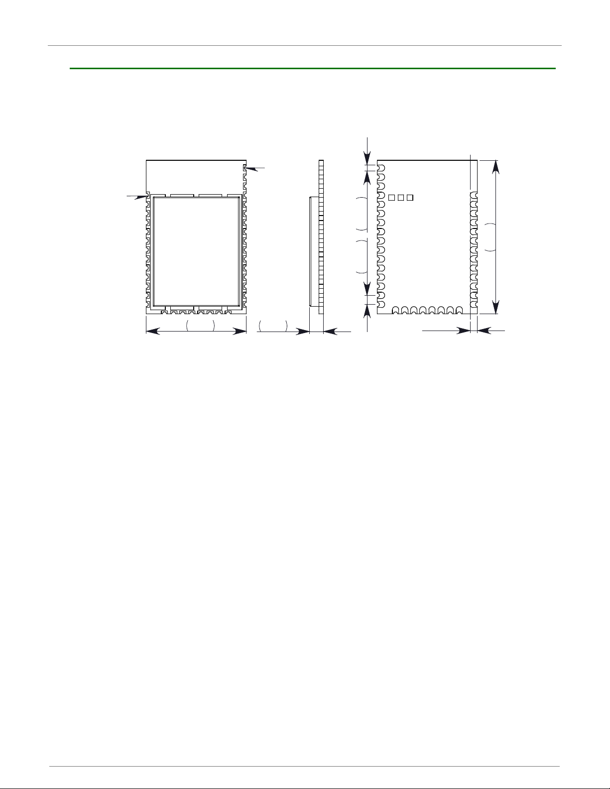
Mechanical Drawings of the XBee ZigBee RF Module
MechanicaldrawingsoftheXBee®/XBee‐PRO®ZBRFModules(antennaoptionsnotshown).Alldimensionsareininches.
.
©2014DigiInternationalInc. 11
Page 12

XBee®/XBee‐PRO®ZBRFModules
Pin Signals for the XBee ZigBee Surface Mount Module
PinAssignmentsforXBeeSurfaceMountModules
Pin # Name Direction Default State Description
1 GND - - Ground
2 VCC - - Power Supply
3 DOUT / DIO13 Both Output UART Data Out / GPIO
4 DIN / CONFIG
5 DIO12 Both GPIO
6 RESET
7 RSSI PWM / DIO10 Both Output RX Signal Strength Indicator / GPIO
8 PWM1 / DIO11 Both Disabled Pulse Width Modulator / GPIO
9 [reserved] - Disabled Do Not Connect
10 DTR
11 GND - - Ground
12 SPI_ATTN
13 GND - - Ground
14 SPI_CLK / DIO18 Input Input Serial Peripheral Interface Clock / GPIO
15 SPI_SSEL
16 SPI_MOSI / DIO16 Input Input Serial Peripheral Interface Data In / GPIO
17 SPI_MISO / DIO15 Output Output Serial Peripheral Interface Data Out / GPIO
18 [reserved]* - Disabled Do Not Connect
19 [reserved]* - Disabled Do Not Connect
20 [reserved]* - Disabled Do Not Connect
21 [reserved]* - Disabled Do Not Connect
22 GND - - Ground
23 [reserved] - Disabled Do Not Connect
24 DIO4 Both Disabled GPIO
25 CTS
26 ON / SLEEP
27 VREF Input -
28 ASSOCIATE / DIO5 Both Output Associate Indicator / GPIO
29 RTS
30 AD3 / DIO3 Both Disabled Analog Input / GPIO
31 AD2 / DIO2 Both Disabled Analog Input / GPIO
32 AD1 / DIO1 Both Disabled Analog Input / GPIO
33 AD0 / DIO0 Both Input Analog Input / GPIO / Commissioning Button
34 [reserved] - Disabled Do Not Connect
35 GND - - Ground
36 RF Both - RF IO for RF Pad Variant
37 [reserved] - Disabled Do Not Connect
/ SLEEP_RQ / DIO8 Both Input Pin Sleep Control Line / GPIO
/ BOOTMODE / DIO19 Output Output
(Low‐assertedsignalsaredistinguishedwithahorizontallineabovesignalname.)
/ DIO14 Both Input UART Data In / GPIO
Input Module Reset
Serial Peripheral Interface Attention
Do not tie low on reset
/ DIO 17 Input Input Serial Peripheral Interface not Select / GPIO
/ DIO7 Both Output Clear to Send Flow Control / GPIO
/ DIO9 Both Output Module Status Indicator / GPIO
Not used for EM357. Used for programmable
secondary processor. For compatibility with other
XBee modules, we recommend connecting this pin
to the voltage reference if Analog Sampling is
desired. Otherwise, connect to GND.
/ DIO6 Both Input Request to Send Flow Control / GPIO
• Signal Direction is specified with respect to the module
• See Design Notes section below for details on pin connections.
• * Refer to the Writing Custom Firmware section for instructions on using these pins if JTAG
functions are needed.
©2014DigiInternationalInc. 12
Page 13

XBee®/XBee‐PRO®ZBRFModules
Pin Signals for the XBee ZigBee Through-hole Module
PinAssignmentsforXBeeThrough‐holeModules
Pin # Name Direction Default State Description
1 VCC - - Power Supply
2 DOUT / DIO13 Both Output UART Data Out
3 DIN / CONFIG
4 DIO12 / SPI_MISO Both Disabled GPIO/ SPI slave out
5 RESET
6 RSSI PWM / PWMO DIO10 Both Output RX signal strength indicator / GPIO
7 PWM1 / DIO11 Both Disabled GPIO
8 [reserved] - - Do Not Connect
9DTR
10 GND - - Ground
11 SPI_MOSI / DIO4 Both Disabled GPIO/ SPI slave in
12 CTS
13 ON_SLEEP
14 VREF - - Not connected
15 ASSOCIATE / DIO5 Both Output Associate Indicator / GPIO
16 RTS
17 AD3 / DIO3 / SPI_SSE
18 AD2 / DIO2 / SPI_CLK Both Disabled Analog Input / GPIO / SPI Clock
19 AD1 / DIO1 / SPI_ATTN
20 AD0 / DIO0 / CB Both Disabled Analog Input / GPIO / Commissioning Button
/ SLEEP_RQ / DIO8 Both Input Pin Sleep Control Line / GPIO
(Low‐assertedsignalsaredistinguishedwithahorizontallineabovesignalname.)
/ DIO14 Both Input UART Data In
Input Input Module Reset
/ DIO7 Both Output Clear-to-Send Flow Control / GPIO
/ DIO9 Both Output Module Status Indicator / GPIO
/ DIO6 Both Input Request to Send Flow Control / GPIO
L Both Disabled Analog Input / GPIO / SPI Slave Select
Both Disabled Analog Input / GPIO / SPI Attention
©2014DigiInternationalInc. 13
Page 14

XBee®/XBee‐PRO®ZBRFModules
EM357 Pin Mappings
The following table shows how the EM357 pins are used on the XBee.
EM357 Pin # EM357 Pin Name XBee (SMT) Pad # XBee (TH) Pin # Other Usage
12 RST 6 5 Programming
18 PA7 8 7
19 PB3 29 16 Used for UART
20 PB4 25 12 Used for UART
21 PA0 / SC2MOSI 16 11 Used for SPI
22 PA1 / SC2MISO 17 4 Used for SPI
24 PA2 / SC2SCLK 14 18 Used for SPI
25 PA3 / SC2SSEL
26 PA4 / PTI_EN 32 19 OTA packet tracing
27
29 PA6 7 6
30 PB1 / SC1TXD 3 2 Used for UART
31 PB2 / SC1RXD 4 3 Used for UART
33 PC2 / JTDO / SWO 26 13 JTAG (see Writing Custom Firmware section)
34 PC3 / JTDI 28 15 JTAG (see Writing Custom Firmware section)
35 PC4 / JTMS / SWDIO 5 4 JTAG (see Writing Custom Firmware section)
36 PB0 10 9
38 PC1 / ADC3 30 17
41 PB7 / ADC2 31 18
42 PB6 / ADC1 33 20
43 PB5 / ADC0 Temperature sensor on PRO version
PA5 / PTI_DATA /
BOOTMODE
15 17 Used for SPI
12 NA
OTA pacet tracing, force embedded serial bootloader, and SPI
attention line
NOTE: Some lines may not go to the external XBee pins in the programmable secondary processor version.
Design Notes for the XBee ZigBee RF Module
The XBee modules do not specifically require any external circuitry or specific connections for proper
operation. However, there are some general design guidelines that are recommended for help in
troubleshooting and building a robust design.
Power Supply Design
Poor power supply can lead to poor radio performance, especially if the supply voltage is not kept within
tolerance or is excessively noisy. To help reduce noise, we recommend placing both a 1F and 8.2pF capacitor
as near to (pad 2/SMT, pin 1/TH) on the PCB as possible. If using a switching regulator for your power supply,
switching frequencies above 500kHz are preferred. Power supply ripple should be limited to a maximum 50mV
peak to peak.
Note – For designs using the programmable modules, an additional 10F decoupling cap is recommended near
(pad 2/SMT, pin 1/TH) of the module. The nearest proximity to (pad 2/SMT, pin 1/TH) of the three caps should
be in the following order: 8.2pf, 1F followed by 10F.
Recommended Pin Connections
The only required pin connections are VCC, GND, DOUT and DIN. To support serial firmware updates, VCC,
GND, DOUT, DIN, RTS, and DTR should be connected.
All unused pins should be left disconnected. All inputs on the radio can be pulled high or low with 30k internal
pull-up or pull-down resistors using the PR and PD software commands. No specific treatment is needed for
unused outputs.
©2014DigiInternationalInc. 14
Page 15

XBee®/XBee‐PRO®ZBRFModules
For applications that need to ensure the lowest sleep current, unconnected inputs should never be left
floating. Use internal or external pull-up or pull-down resistors, or set the unused I/O lines to outputs.
Other pins may be connected to external circuitry for convenience of operation, including the Associate LED
pad (pad 28/SMT, pin 15/TH) and the Commissioning pad (pad 33/SMT, pin 20/TH). The Associate LED pad
will flash differently depending on the state of the module to the network, and a pushbutton attached to pad
33 can enable various join functions without having to send serial port commands. Please see the
commissioning pushbutton and associate LED section in chapter 7 for more details. The source and sink
capabilities are limited to 4mA for pad numbers 3, 4, 5, 10, 12, 14, 15, 16, 17, 25, 26, 28, 29, 30 and 32, and
8mA for pad numbers 7, 8, 24, 31 and 33 on the SMT module. The source and sink capabilities are limited to
4mA for pin numbers 2, 3, 4, 9, 12, 13, 15, 16, 17, and 19, and 8mA for pin numbers 6, 7, 11, 18, and 20 on
the TH module.
The VRef pad (pad 27) is only used on the programmable versions of the SMT modules. For the TH modules, a
VRef pin (Pin #14) is used. For compatibility with other XBee modules, we recommend connecting this pin to
a voltage reference if analog sampling is desired. Otherwise, connect to GND.
Board Layout
XBee modules are designed to be self sufficient and have minimal sensitivity to nearby processors, crystals or
other PCB components. As with all PCB designs, Power and Ground traces should be thicker than signal traces
and able to comfortably support the maximum current specifications. A recommended PCB footprint for the
module can be found in Appendix C. No other special PCB design considerations are required for integrating
XBee radios except in the antenna section.
The choice of antenna and antenna location is very important for correct performance. With the exception of
the RF Pad variant, XBees do not require additional ground planes on the host PCB. In general, antenna
elements radiate perpendicular to the direction they point. Thus a vertical antenna emits across the horizon.
Metal objects near the antenna cause reflections and may reduce the ability for an antenna to radiate
efficiently. Metal objects between the transmitter and receiver can also block the radiation path or reduce the
transmission distance, so external antennas should be positioned away from them as much as possible. Some
objects that are often overlooked are metal poles, metal studs or beams in structures, concrete (it is usually
reinforced with metal rods), metal enclosures, vehicles, elevators, ventilation ducts, refrigerators, microwave
ovens, batteries, and tall electrolytic capacitors.
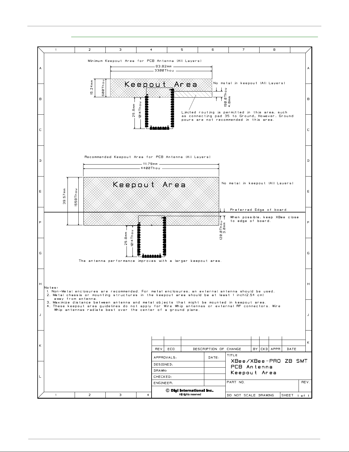
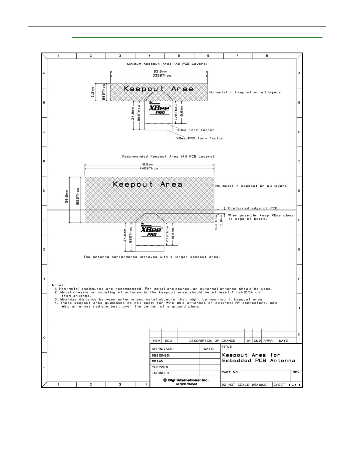
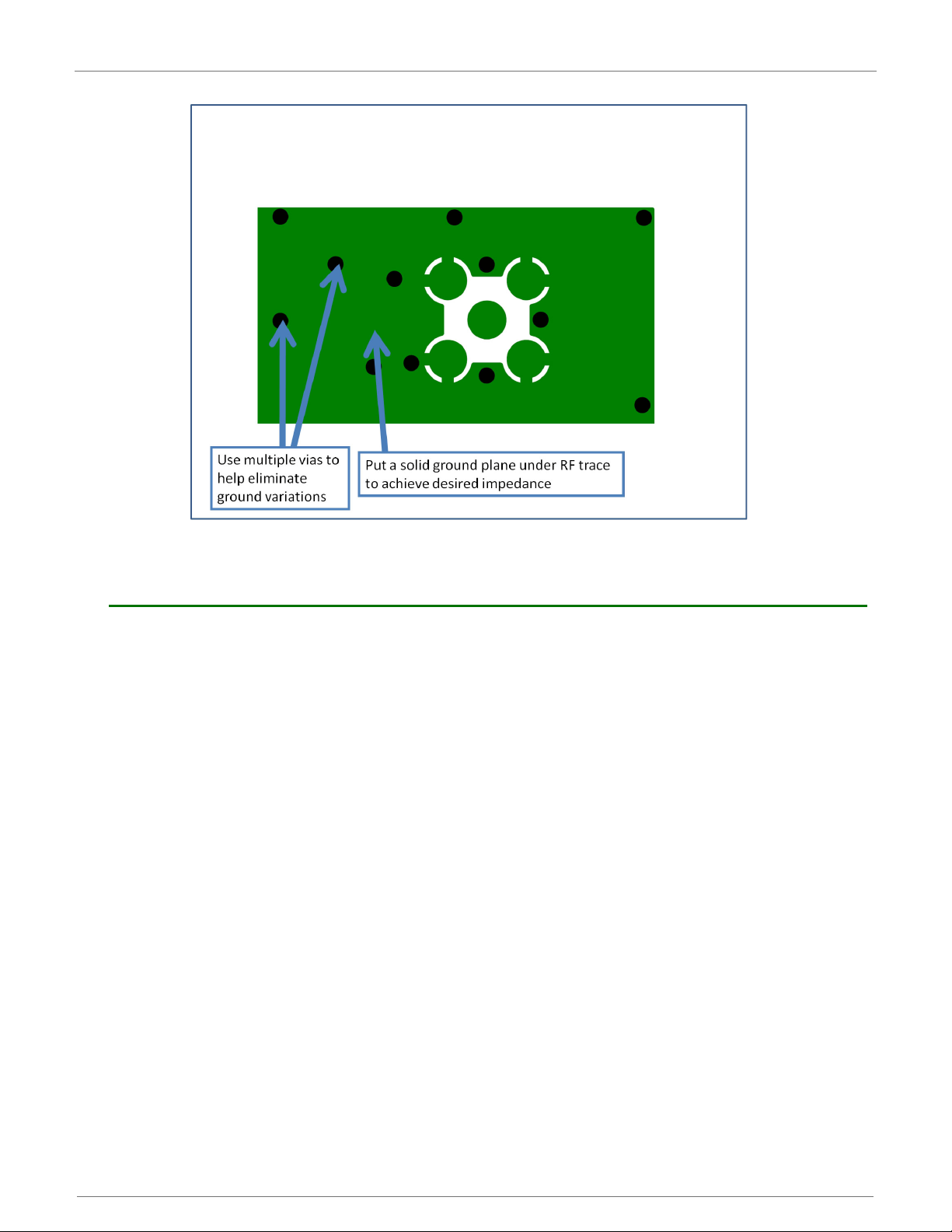
Design Notes for PCB Antenna Modules
PCB Antenna modules should not have any ground planes or metal objects above or below the antenna.
For best results, the module should not be placed in a metal enclosure, which may greatly reduce the
range. The module should be placed at the edge of the PCB on which it is mounted. The ground, power
and signal planes should be vacant immediately below the antenna section. The drawings on the
following pages illustrate important recommendations when designing with PCB antenna modules. It
should be noted that for optimal performance, this module should not be mounted on the RF Pad
footprint described in the next section because the footprint requires a ground plane within the PCB
Antenna keep out area.
©2014DigiInternationalInc. 15
Page 16
XBee®/XBee‐PRO®ZBRFModules
SMT Keepout Area
©2014DigiInternationalInc. 16
Page 17
XBee®/XBee‐PRO®ZBRFModules
TH Keepout Area
©2014DigiInternationalInc. 17
Page 18
XBee®/XBee‐PRO®ZBRFModules
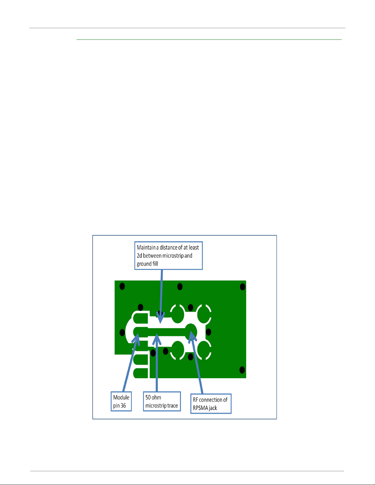
Design Notes for SMT RF Pad Modules
The RF Pad is a soldered antenna connection. The RF signal travels from pin 36 on the module to the
antenna through an RF trace transmission line on the PCB. Please note that any additional components
between the module and antenna will violate modular certification. The RF trace should have a
controlled impedance of 50 ohms. We recommend using a microstrip trace, although coplanar
waveguide may also be used if more isolation is needed. Microstrip generally requires less area on the
PCB than coplanar waveguide. Stripline is not recommended because sending the signal to different PCB
layers can introduce matching and performance problems.
It is essential to follow good design practices when implementing the RF trace on a PCB. The following
figures show a layout example of a host PCB that connects an RF Pad module to a right angle, through
hole RPSMA jack. The top two layers of the PCB have a controlled thickness dielectric material in
between. The second layer has a ground plane which runs underneath the entire RF Pad area. This
ground plane is a distance d, the thickness of the dielectric, below the top layer. The top layer has an RF
trace running from pin 36 of the module to the RF pin of the RPSMA connector. The RF trace's width
determines the impedance of the transmission line with relation to the ground plane. Many online tools
can estimate this value, although the PCB manufacturer should be consulted for the exact width.
Assuming d=0.025", and that the dielectric has a relative permittivity of 4.4, the width in this example
will be approximately 0.045" for a 50 ohm trace. This trace width is a good fit with the module
footprint's 0.060" pad width. Using a trace wider than the pad width is not recommended, and using a
very narrow trace (under 0.010") can cause unwanted RF loss. The length of the trace is minimized by
placing the RPSMA jack close to the module. All of the grounds on the jack and the module are
connected to the ground planes directly or through closely placed vias. Any ground fill on the top layer
should be spaced at least twice the distance d (in this case, at least 0.050") from the microstrip to
minimize their interaction.
Implementing these design suggestions will help ensure that the RF Pad module performs to its
specifications.
PCBLayer1ofRFLayoutExample
©2014DigiInternationalInc. 18
Page 19
XBee®/XBee‐PRO®ZBRFModules
PCBLayer2ofRFLayoutExample
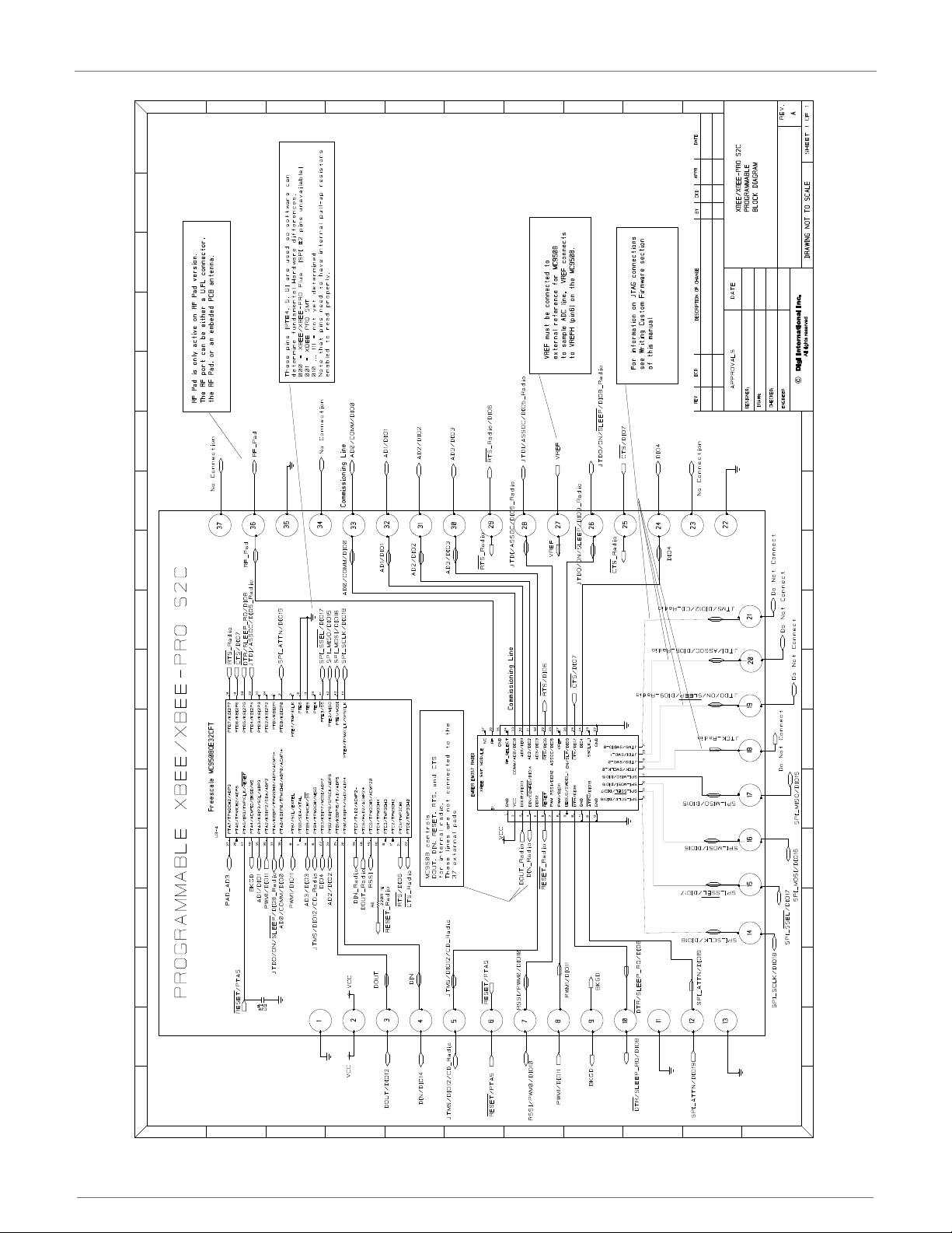
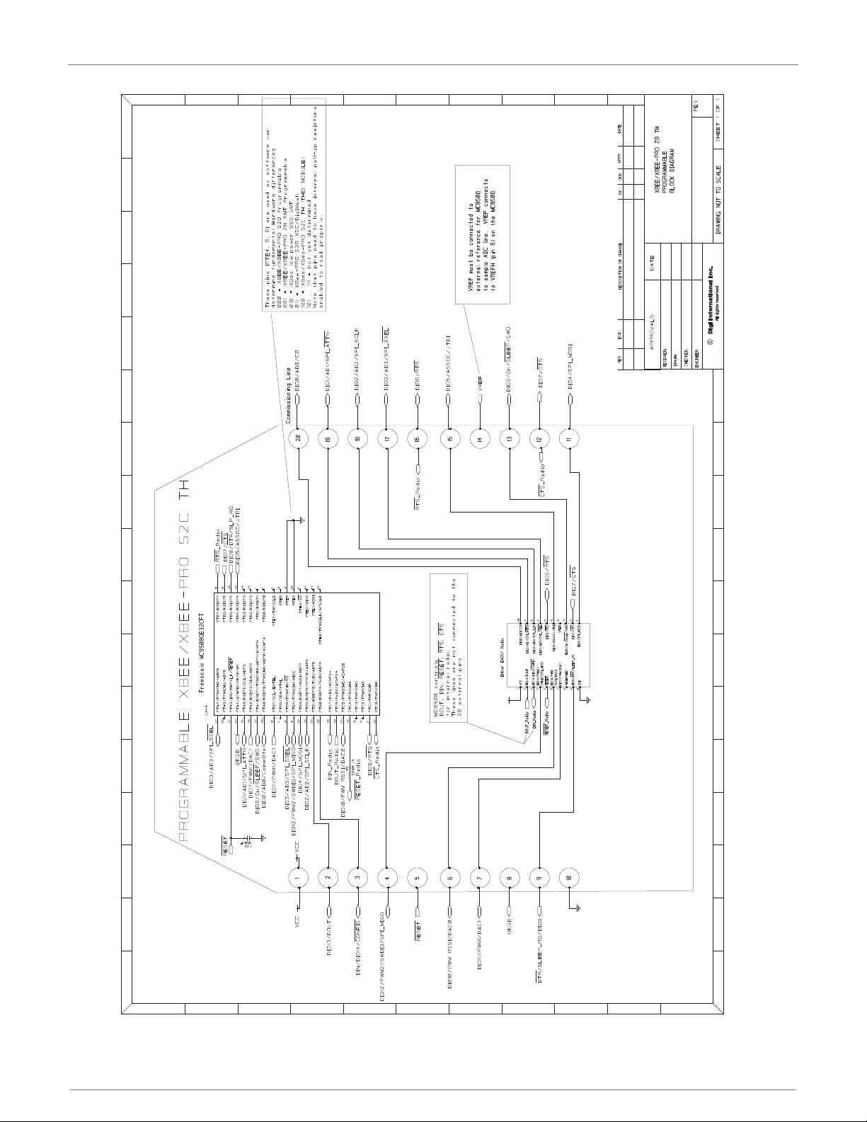
Module Operation for Programmable Variant
The modules with the programmable option have a secondary processor with 32k of flash and 2k of RAM. This
allows module integrators to put custom code on the XBee module to fit their own unique needs. The DIN,
DOUT, RTS, CTS, and RESET lines are intercepted by the secondary processor to allow it to be in control of the
data transmitted and received. All other lines are in parallel and can be controlled by either the EM357 or the
MC9SO8QE micro (see Block Diagram for details). The EM357 by default has control of certain lines. These
lines can be released by the EM357 by sending the proper command(s) to disable the desired DIO line(s) (see
XBee Command Reference Tables).
In order for the secondary processor to sample with ADCs, the XBee VREF pin (27/SMT, 14/TH) must be
connected to a reference voltage.
Digi provides a bootloader that can take care of programming the processor over the air or through the serial
interface. This means that over the air updates can be supported through an XMODEM protocol. The processor
can also be programmed and debugged through a one wire interface BKGD (Pin 9/SMT, Pin 8/TH).
©2014DigiInternationalInc. 19
Page 20
XBee®/XBee‐PRO®ZBRFModules
©2014DigiInternationalInc. 20
Page 21
XBee®/XBee‐PRO®ZBRFModules
©2014DigiInternationalInc. 21
Page 22

XBee®/XBee‐PRO®ZBRFModules
XBee Programmable Bootloader
Overview
The XBee Programmable module is equipped with a Freescale MC9S08QE32 application processor. This
application processor comes with a supplied bootloader. This section describes how to interface the customer's
application code running on this processor to the XBee Programmable module's supplied bootloader.
The first section discusses how to initiate firmware updates using the supplied bootloader for wired and overthe-air updates.
Bootloader Software Specifics
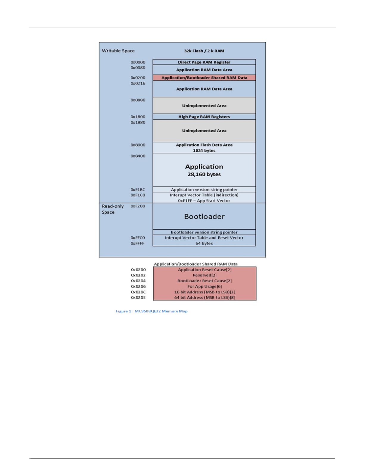
Memory Layout
Figure 1 shows the memory map for the MC9S08QE32 application processor.
The supplied bootloader occupies the bottom pages of the flash from 0xF200 to 0xFFFF. Application
code cannot write to this space.
The application code can exist in Flash from address 0x8400 to 0xF1BC. 1k of Flash from 0x8000 to
0x83FF is reserved for Non Volatile Application Data that will not be erased by the bootloader during a
flash update.
A portion of RAM is accessible by both the application and the bootloader. Specifically, there is a shared
data region used by both the application and the bootloader that is located at RAM address 0x200 to
0x215. Application code should not write anything to BLResetCause or AppResetCause unless
informing the bootloader of the impending reset reason. The Application code should not clear
BLResetCause unless it is handling the unexpected reset reason.
To prevent a malfunctioning application from running forever, the Bootloader increments BLResetCause
after each watchdog or illegal instruction reset. If this register reaches above 0x10 the bootloader will
stop running the application for a few minutes to allow an OTA or Local update to occur. If no update is
initiated within the time period, BLResetCause is cleared and the application is started again. To
prevent unexpected halting of the application, the application shall clear or decrement BLResetCause
just before a pending reset. To disable this feature, the application shall clear BLResetCause at the
start of the application.
©2014DigiInternationalInc. 22
Page 23
XBee®/XBee‐PRO®ZBRFModules
©2014DigiInternationalInc. 23
Page 24

XBee®/XBee‐PRO®ZBRFModules
Operation
Upon reset of any kind, the execution control begins with the bootloader.
If the reset cause is Power-On reset (POR), Pin reset (PIN), or Low Voltage Detect (LVD) reset (LVD)
the bootloader will not jump to the application code if the override bits are set to RTS(D7)=1,
DTR(D5)=0, and DIN(B0)=0. Otherwise, the bootloader writes the reset cause "NOTHING" to the
shared data region, and jumps to the Application.
Reset causes are defined in the file common. h in an enumeration with the following definitions:
typedef enum {
BL_CAUSE_NOTHING = 0x0000, //PIN, LVD, POR
BL_CAUSE_NOTHING_COUNT = 0x0001,//BL_Reset_Cause counter
// Bootloader increments cause every reset
BL_CAUSE_BAD_APP = 0x0010,//Bootloader considers APP invalid
} BL_RESET_CAUSES;
typedef enum {
APP_CAUSE_NOTHING = 0x0000,
APP_CAUSE_USE001 = 0x0001,
// 0x0000 to 0x00FF are considered valid for APP use.
APP_CAUSE_USE255 = 0x00FF,
APP_CAUSE_FIRMWARE_UPDATE = 0x5981,
APP_CAUSE_BYPASS_MODE = 0x4682,
APP_CAUSE_BOOTLOADER_MENU = 0x6A18,
} APP_RESET_CAUSES;
Otherwise, if the reset cause is a "watchdog" or other reset, the bootloader checks the shared memory
region for the APP_RESET_CAUSE. If the reset cause is:
1."APP_CAUSE_NOTHING" or 0x0000 to 0x00FF, the bootloader increments the
BL_RESET_CAUSES, verifies that it is still less than BL_CAUSE_BAD_APP, and jumps back to
the application. If the Application does not clear the BL_RESET_CAUSE, it can prevent an
infinite loop of running a bad application that continues to perform illegal instructions or
watchdog resets.
2."APP_CAUSE_FIRMWARE_UPDATE", the bootloader has been instructed to update the
application "over-the-air" from a specific 64-bit address. In this case, the bootloader will
attempt to initiate an Xmodem transfer from the 64-bit address located in shared RAM.
3."APP_CAUSE_BYPASS_MODE", the bootloader executes bypass mode. This mode passes the
local UART data directly to the EM357 allowing for direct communication with the EM357.
The only way to exit bypass mode is to reset or power cycle the module.
If none of the above is true, the bootloader will enter "Command mode". In this mode, users can
initiate firmware downloads both wired and over-the-air, check application/bootloader version strings,
and enter Bypass mode.
Application version string
Figure 1 shows an "Application version string pointer" area in application flash which holds the pointer
to where the application version string resides. The application's linker command file ultimately
determines where this string is placed in application flash.
It is preferable that the application version string be located at address 0x8400 for MC9S08QE32 parts.
The application string can be any characters terminated by the NULL character (0x00). There is not a
strict limit on the number of characters in the string, but for practical purposes should be kept under
100 bytes including the terminating NULL character. During an update the bootloader erases the entire
application from 0x8400 on. The last page has the vector table specifically the redirected reset vector.
The version string pointer and reset vector are used to determine if the application is valid.
©2014DigiInternationalInc. 25
Page 25

XBee®/XBee‐PRO®ZBRFModules
Application Interrupt Vector table and Linker Command File
Since the bootloader flash region is read-only, the interrupt vector table is redirected to the region
0xF1C0 to 0xF1FD so that application developers can use hardware interrupts. Note that in order for
Application interrupts to function properly, the Application's linker command file (*.prm extension)
must be modified appropriately to allow the linker to place the developers code in the correct place in
memory. For example, the developer desires to use the serial communications port SCI1 receive
interrupt. The developer would add the following line to the Codewarrior linker command file for the
project:
VECTOR ADDRESS 0x0000F1E0 vSci1Rx
This will inform the linker that the interrupt function "vSci1Rx()" should be placed at address
0x0000F1E0. Next, the developer should add a file to their project "vector_table.c" that creates an
array of function pointers to the ISR routines used by the application.
extern void _Startup(void);/* _Startup located in Start08.c */
extern void vSci1Rx(void);/* sci1 rx isr */
extern short iWriteToSci1(unsigned char *);
void vDummyIsr(void);
#pragma CONST_SEG VECTORS
void (* const vector_table[])(void) = /* Relocated Interrupt vector table */{
vDummyIsr,/* Int.no. 0 Vtpm3ovf (at F1C0)Unassigned */
vDummyIsr, /* Int.no. 1 Vtpm3ch5 (at F1C2) Unassigned */
vDummyIsr, /* Int.no. 2 Vtpm3ch4 (at F1C4) Unassigned */
vDummyIsr, /* Int.no. 3 Vtpm3ch3 (at F1C6) Unassigned */
vDummyIsr, /* Int.no. 4 Vtpm3ch2 (at F1C8) Unassigned */
vDummyIsr, /* Int.no. 5 Vtpm3ch1 (at F1CA) Unassigned */
vDummyIsr, /* Int.no. 6 Vtpm3ch0 (at F1CC) Unassigned */
vDummyIsr, /* Int.no. 7 Vrtc (at F1CE) Unassigned */
vDummyIsr, /* Int.no. 8 Vsci2tx (at F1D0) Unassigned */
vDummyIsr, /* Int.no. 9 Vsci2rx (at F1D2) Unassigned */
vDummyIsr, /* Int.no. 10 Vsci2err (at F1D4) Unassigned */
vDummyIsr, /* Int.no. 11 Vacmpx (at F1D6) Unassigned */
vDummyIsr, /* Int.no. 12 Vadc (at F1D8) Unassigned */
vDummyIsr, /* Int.no. 13 Vkeyboard (at F1DA) Unassigned */
vDummyIsr, /* Int.no. 14 Viic (at F1DC) Unassigned */
vDummyIsr, /* Int.no. 15 Vsci1tx (at F1DE) Unassigned */
vSci1Rx, /* Int.no. 16 Vsci1rx (at F1E0) SCI1RX */
vDummyIsr, /* Int.no. 17 Vsci1err (at F1E2) Unassigned */
vDummyIsr, /* Int.no. 18 Vspi (at F1E4) Unassigned */
vDummyIsr, /* Int.no. 19 VReserved12 (at F1E6) Unassigned */
vDummyIsr, /* Int.no. 20 Vtpm2ovf (at F1E8) Unassigned */
vDummyIsr, /* Int.no. 21 Vtpm2ch2 (at F1EA) Unassigned */
vDummyIsr, /* Int.no. 22 Vtpm2ch1 (at F1EC) Unassigned */
vDummyIsr, /* Int.no. 23 Vtpm2ch0 (at F1EE) Unassigned */
vDummyIsr, /* Int.no. 24 Vtpm1ovf (at F1F0) Unassigned */
vDummyIsr, /* Int.no. 25 Vtpm1ch2 (at F1F2) Unassigned */
vDummyIsr, /* Int.no. 26 Vtpm1ch1 (at F1F4) Unassigned */
vDummyIsr, /* Int.no. 27 Vtpm1ch0 (at F1F6) Unassigned */
©2014DigiInternationalInc. 26
Page 26

XBee®/XBee‐PRO®ZBRFModules
};
void vDummyIsr(void){
for(;;){
if(iWriteToSci1("STUCK IN UNASSIGNED ISR\n\r>"));
}
}
The interrupt routines themselves can be defined in separate files. The "vDummyIsr" function is used
in conjunction with "iWritetoSci1" for debugging purposes.
Bootloader Menu Commands
The bootloader accepts commands from both the local UART and OTA. All OTA commands sent must be
Unicast with only 1 byte in the payload for each command. A response will be returned to the sender. All
Broadcast and multiple byte OTA packets are dropped to help prevent general OTA traffic from being
interpreted as a command to the bootloader while in the menu.
Bypass Mode - "B"
vDummyIsr, /* Int.no. 28 Vlvd (at F1F8) Unassigned */
vDummyIsr, /* Int.no. 29 Virq (at F1FA) Unassigned */
vDummyIsr, /* Int.no. 30 Vswi (at F1FC) Unassigned */
_Startup /* Int.no. 31 Vreset (at F1FE) Reset vector */
The bootloader provides a "bypass" mode of operation that essentially connects the SCI1 serial
communications peripheral of the freescale mcu to the EM357's serial Uart channel. This allows direct
communication to the EM357 radio for the purpose of firmware and radio configuration changes. Once
in bypass mode, the XCTU utility can change modem configuration and/or update EM357 firmware.
Bypass mode automatically handles any baud rate up to 115.2kbps. Note that this command is
unavailable when module is accessed remotely.
Update Firmware - "F"
The "F" command initiates a firmware download for both wired and over-the-air configurations.
Depending on the source of the command (received via Over the Air or local UART), the download will
proceed via wired or over-the-air respectively.
Adjust Timeout for Update Firmware - "T"
The "T" command changes the timeout before sending a NAK by Base-Time*2^(T). The Base-Time for
the local UART is different than the Base-Time for Over the Air. During a firmware update, the
bootloader will automatically increase the Timeout if repeat packets are received or multiple NAKs for
the same packet without success occur.
Application Version String - "A"
The "A" command provides the version of the currently loaded application. If no application is present,
"Unkown" will be returned.
Bootloader Version String - "V"
The "V" command provides the version of the currently loaded bootloader. The version will return a
string in the format BLFFF-HHH-XYZ_DDD where FFF represents the Flash size in kilo bytes, HHH is the
hardware, XYZ is the version, and DDD is the preferred XMODEM packet size for updates. Double the
preferred packet size is also possible, but not guaranteed. For example "BL032-2B0-023_064" will take
64 byte CRC XMODEM payloads and may take 128 byte CRC XMODEM payloads also. In this case, both
64 and 128 payloads are handled, but the 64 byte payload is preferred for better Over the Air
reliability.
Bootloader Version BL032-2x0-025_064 only operates at 9600 baud on the local UART as well as
communications to the EM357 Radio. A newer version of the Bootloader BL032-2x0-033_064 or newer
BL032-2B0-XXX_064 has changed the baud rate to 115200 between the Programmable and the EM357
©2014DigiInternationalInc. 27
Page 27

XBee®/XBee‐PRO®ZBRFModules
Radio. The EM357 is also set to 115200 as the default baud rate. The default rate of the programmable
local UART is also set to 115200, however, the local UART has an auto baud feature added to detect if
the UART is at the wrong baud rate. If a single character is sent, it will automatically switch to 115200
or 9600 baud.
Firmware Updates
Wired Updates
A user can update their application using the bootloader in a wired configuration with the following
steps:
a. Plug XBee programmable module into a suitable serial port on a PC.
b. Open a hyperterminal (or similar dumb terminal application) session with 115200 baud, no parity, and 8 data bits with one stop bit.
c. Hit Enter to display the bootloader menu.
d. Hit the "F" key to initiate a wired firmware update.
e. A series of "C" characters Will be displayed within the hyperterminal window. At this point,
select the "transfer->send file" menu item. Select the desired flat binary output file.
f. Select "Xmodem" as the protocol.
g. Click "Send" on the "Send File" dialog. The file will be downloaded to the XBee Programmable
module. Upon a successful update, the bootloader will jump to the newly loaded application.
Over-The-Air updates
A user can update their application using the bootloader in an "over-the-air" configuration with the
following steps…(This procedure assumes that the bootloader is running and not the application. The
EM357 baud rate of the programmable module must be set to 115200 baud. The
bootloader only operates at 115200 baud between the Radio and programmable bootloader. The
application must be programmed with some way to support returning to the bootloader in order to
support Over the Air (OTA) updates without local intervention.)
a. The XBee module sending the file OTA (Host module) should be set up with a series 2 Xbee
module with transparent mode firmware.
b. The XBee Programmable module receiving the update (remote module) is configured with API
firmware.
c. Open a hyperterminal session to the host module with no parity, no hardwareflow control, 8
data bits and 1 stop bit. (The host module does not have to operate at the same baud rate as the
remote module.) For faster updates and less latency due to the UART, set the host module to a
faster baud rate. (i.e. 115200)
d.Enter 3 pluses "+++" to place the EM357 in command mode. (or XCTU’s “Modem Configuration”
tab can be used to set the correct parameters)
e. Set the Host Module destination address to the target module’s 64 bit address that the host
module will update (ATDH aabbccdd, ATDL eeffgghh, ATCN, where aabbccddeeffgghh is the hexadecimal 64 bit address of the target module).
f. Hit Enter and the bootloader command menu will be displayed from the remote module. (Note
that the option "B" doesn't exist for OTA)
g. Hit the "F" key to cause the remote module to request the new firmware file over-the-air.
h. The host module will begin receiving "C" characters indicating that the remote module is
requesting an Xmodem CRC transfer. Using XCTU or another terminal program, Select "XMODEM"
file transfer. Select the Binary file to upload/transfer. Click Send to start the transfer. At the conclusion of a successful transfer, the bootloader will jump to the newly loaded application.
©2014DigiInternationalInc. 28
Page 28

XBee®/XBee‐PRO®ZBRFModules
Output File Configuration
BKGD Programming
P&E Micro provides a background debug tool that allows flashing applications on the MC9S08QE parts
through their background debug mode port. By default, the Codewarrior tool produces an "ABS" output
file for use in programming parts through the background debug interface. The programmable XBee
from the factory has the BKGD debugging capability disabled. In order to debug, a bootloader with the
debug interface enabled needs to be loaded on the secondary processor or a stand-alone app needs to
be loaded.
Bootloader updates
The supplied bootloader requires files in a "flat binary" format which differs from the default ABS file
produced. The Codewarrior tool also produces a S19 output file. In order to successfully flash new
applications, the S19 file must be converted into the flat binary format. Utilities are available on the
web that will convert S19 output to "BIN" outputs. Often times, the "BIN" file conversion will pad the
addresses from 0x0000 to the code space with the same number. (Often 0x00 or 0xFF) These extra
bytes before the APP code starts will need to be deleted from the bin file before the file can be
transferred to the bootloader.
©2014DigiInternationalInc. 29
Page 29
2.XBeeZigBeeRFModuleOperation
DIN (data in)
DIN (data in)
DOUT (data out )
DOUT (data out)
XBee ZigBee Serial Communications
XBee RF Modules interface to a host device through a serial port. Through its serial port, the module can
communicate with any logic and voltage compatible UART, through a level translator to any serial device (for
example, through a RS-232 or USB interface board), or through a Serial Peripheral Interface, which is a synchronous
interface to be described later.
Two Wire serial Interface (TWI) is also available, but not supported by Digi. For information on the TWI, see the
EM357 specification.
UART Data Flow
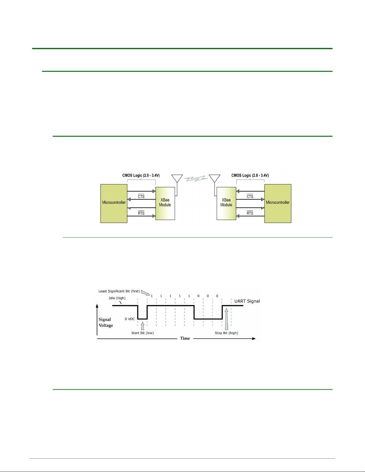
Devices that have a UART interface can connect directly to the pins of the RF module as shown in the figure
below.
SystemDataFlowDiagraminaUART‐interfacedenvironment
(Low‐assertedsignalsdistinguishedwithhorizontallineoversignalname.)
Serial Data
Data enters the module UART through the DIN (pin 4) as an asynchronous serial signal. The signal should
idle high when no data is being transmitted.
Each data byte consists of a start bit (low), 8 data bits (least significant bit first) and a stop bit (high). The
following figure illustrates the serial bit pattern of data passing through the module.
UARTdatapacket0x1F(decimalnumberʺ31ʺ)astransmittedthroughtheRFmodule
ExampleDataFormatis8‐N‐1(bits‐parity‐#ofstopbits)
Serial communications depend on the two UARTs (the microcontroller's and the RF module's) to be
configured with compatible settings (baud rate, parity, start bits, stop bits, data bits).
The UART baud rate, parity, and stop bits settings on the XBee module can be configured with the BD, NB,
and SB commands respectively. See the command table in chapter 10 for details.
XBee ZigBee SPI Communications
The XBee modules support SPI communications in slave mode. Slave mode receives the clock signal and data
from the master and returns data to the master. The SPI port uses the following signals on the XBee:
• SPI_MOSI (Master Out, Slave In) - inputs serial data from the master
• SPI_MISO (Master In, Slave Out) - outputs serial data to the master
• SPI_SCLK (Serial Clock) - clocks data transfers on MOSI and MISO
©2014DigiInternationalInc. 30
Page 30
XBee®/XBee‐PRO®ZBRFModules
•SPI_SSEL (Slave Select) - enables serial communication with the slave
The above four pins are standard for SPI. This module also supports an additional pin, which may be configured
to alert the SPI master when it has data to send. This pin is called SPI_ATTN
(through polling or interrupts), it can know when it needs to receive data from the module. SPI_ATTN
whenever it has data to send and it remains asserted until all available data has been shifted out to the SPI
master.
In this mode, the following apply:
• Data/Clock rates of up to 5 Mbps are possible
• Data is MSB first
• Frame Format mode 0 is used (see below)
. If the master monitors this pin
asserts
FrameFormatforSPICommunications
SPI Operation
When the slave select (SPI_SSEL) signal is asserted by the master, SPI transmit data is driven to the output
pin (SPI_MISO), and SPI data is received from the input pin SPI_MOSI. The SPI_SSEL
asserted to enable the transmit serializer to drive data to the output signal SPI_MISO. A rising edge on
SPI_SSEL resets the SPI slave shift registers.
If the SPI_SCLK is present, the SPI_MISO line is always driven whether with or without the SPI_SSEL
driven. This is a known issue with the Ember EM357 chip, and makes additional hardware necessary if
multiple slaves are using the same bus as the XBee.
If the input buffer is empty, the SPI serializer transmits a busy token (0xFF). Otherwise, all transactions on
the SPI port use API operation. See Chapter 9 - API Operation for more information.
The SPI slave controller must guarantee that there is time to move new transmit data from the transmit
buffer into the hardware serializer. To provide sufficient time, the SPI slave controller inserts a byte of
padding at the start of every new string of transmit data. Whenever the transmit buffer is empty and data
is placed into the transmit buffer, the SPI hardware inserts a byte of padding onto the front of the
transmission as if this byte were placed there by software.
Serial Port Selection
In the default configuration the UART and SPI ports will both be configured for serial port operation.
If DOUT is held low during boot, then only SPI will be used. If both interfaces are configured, serial data will
go out the UART until the SPI_SSEL
the SPI interface.
If only the UART is enabled, then only the UART will be used, and SPI_SSEL
is enabled, then only the SPI will be used.
If neither serial port is enabled, the module will not support serial operations and all communications must
occur over the air. All data that would normally go to the serial port is discarded.
signal is asserted. Thereafter, all serial communications will operate on
will be ignored. If only the SPI
pin has to be
line
XBee ZigBee Serial Buffers
The XBee modules maintain small buffers to collect received serial and RF data, which is illustrated in the figure
below. The serial receive buffer collects incoming serial characters and holds them until they can be processed.
©2014DigiInternationalInc. 31
Page 31

XBee®/XBee‐PRO®ZBRFModules
Serial
Receiver
Buffer
RF TX
Buffer
Transmitter
RF Switch
Antenna
Port
Receiver
Serial Transmit
Buffer
RF RX
Buffer
Processor
The serial transmit buffer collects data that is received via the RF link that will be transmitted out the UART or
SPI port.
InternalDataFlowDiagram
DIN or MOSI
CTS
(If D7 is 1 and
UART is in use)
DOUT or MISO
RTS
(If UART is in
use, ignored un-
less D6 is 1)
Serial Receive Buffer
When serial data enters the RF module through the serial port, the data is stored in the serial receive buffer
until it can be processed. Under certain conditions, the module may receive data when the serial receive
buffer is already full. In that case the data is discarded.
The serial receive buffer becomes full when data is streaming into the serial port faster than it can be
processed and sent over the air (OTA). While the speed of receiving the data on the serial port can be
much faster than the speed of transmitting to data for a short period, sustained operation in that mode will
cause data to be dropped due to running out of places in the module to put the data. Some things that
may delay over the air transmissions are address discovery, route discovery, and retransmissions.
Processing received RF data can also take away time and resources for processing incoming serial data.
If the UART is the serial port and CTS flow control is enabled, the external data source is alerted when the
receive buffer is almost full. Then the host holds off sending data to the module until the module asserts
CTS again, allowing more data to come in.
If the SPI is the serial port, no hardware flow control is available. It is the user's responsibility to ensure
that that receive buffer is not overflowed. One reliable strategy is to wait for a TX_STATUS response after
each frame sent to ensure that the module has had time to process it.
Serial Transmit Buffer
When RF data is received, the data is moved into the serial transmit buffer and sent out the UART or SPI
port. If the serial transmit buffer becomes full enough such that all data in a received RF packet won't fit in
the serial transmit buffer, the entire RF data packet is dropped.
Cases in which the serial transmit buffer may become full resulting in dropped RF packets:
1 If the RF data rate is set higher than the interface data rate of the module, the module could
receive data faster than it can send the data to the host.
2 If the host does not allow the module to transmit data out from the serial transmit buffer because
of being held off by hardware flow control.
UART Flow Control
©2014DigiInternationalInc. 32
The RTS and CTS module pins can be used to provide RTS and/or CTS flow control. CTS flow control provides an
indication to the host to stop sending serial data to the module. RTS flow control allows the host to signal the
module to not send data in the serial transmit buffer out the UART. RTS and CTS flow control are enabled using
the D6 and D7 commands. Please note that serial port flow control is not possible when using the SPI port.
Page 32

XBee®/XBee‐PRO®ZBRFModules
CTS Flow Control
If CTS flow control is enabled (D7 command), when the serial receive buffer is 17 bytes away from being
full, the module de-asserts CTS
re-asserted after the serial receive buffer has 34 bytes of space.
RTS Flow Control
If RTS flow control is enabled (D6 command), data in the serial transmit buffer will not be sent out the
DOUT pin as long as RTS
periods of time to avoid filling the serial transmit buffer. If an RF data packet is received, and the serial
transmit buffer does not have enough space for all of the data bytes, the entire RF data packet will be
discarded.
Note: If the XBee is sending data out the UART when RTS is de-asserted (set high), the XBee could send up to 5 characters out the UART or SPI port after RTS is de-asserted.
XBee ZigBee Break Control
If break is enabled for over five seconds, the XBee will reset. Then it will boot with default baud settings into
command mode.
This break function will be disabled if either P3 or P4 are not enabled.
(sets it high) to signal to the host device to stop sending serial data. CTS is
is de-asserted (set high). The host device should not de-assert RTS for long
Serial Interface Protocols
The XBee modules support both transparent and API (Application Programming Interface) serial interfaces.
Transparent Operation
When operating in transparent mode, the modules act as a serial line replacement. All UART or SPI data
received through the DIN or MOSI pin is queued up for RF tra nsmissi on. When RF data is received, the data
is sent out through the serial port. The module configuration parameters are configured using the AT
command mode interface. Please note that transparent operation is not provided when using the SPI.
Data is buffered in the serial receive buffer until one of the following causes the data to be packetized and
transmitted:
•No serial characters are received for the amount of time determined by the RO (Packetization Timeout) parameter. If RO = 0, packetization begins when a character is received.
•The Command Mode Sequence (GT + CC + GT) is received. Any character buffered in the serial
receive buffer before the sequence is transmitted.
•The maximum number of characters that will fit in an RF packet is received.
API Operation
API operation is an alternative to transparent operation. The frame-based API extends the level to which a
host application can interact with the networking capabilities of the module. When in API mode, all data
entering and leaving the module is contained in frames that define operations or events within the module.
Transmit Data Frames (received through the serial port) include:
•RF Transmit Data Frame
•Command Frame (equivalent to AT commands)
Receive Data Frames (sent out the serial port) include:
•RF-received data frame
•Command response
•Event notifications such as reset, associate, disassociate, etc.
The API provides alternative means of configuring modules and routing data at the host application layer. A
host application can send data frames to the module that contain address and payload information instead
of using command mode to modify addresses. The module will send data frames to the application
containing status packets; as well as source, and payload information from received data packets.
©2014DigiInternationalInc. 33
Page 33

XBee®/XBee‐PRO®ZBRFModules
The API operation option facilitates many operations such as the examples cited below:
-> Transmitting data to multiple destinations without entering Command Mode
-> Receive success/failure status of each transmitted RF packet
-> Identify the source address of each received packet
A Comparison of Transparent and API Operation
The following table compares the advantages of transparent and API modes of operation:
Simple Interface All received serial data is transmitted unless the module is in command mode.
Easy to support It is easier for an application to support transparent operation and command mode
Easy to manage data
transmissions to multiple
destinations
Received data frames
indicate the sender's
address
Advanced ZigBee
addressing support
Advanced networking
diagnostics
Remote Configuration
Transparent Operation Features
API Operation Features
Transmitting RF data to multiple remotes only requires changing the address in the API frame. This
process is much faster than in transparent operation where the application must enter AT command
mode, change the address, exit command mode, and then transmit data.
Each API transmission can return a transmit status frame indicating the success or reason for
failure.
All received RF data API frames indicate the source address.
API transmit and receive frames can expose ZigBee addressing fields including source and
destination endpoints, cluster ID and profile ID. This makes it easy to support ZDO commands and
public profile traffic.
API frames can provide indication of IO samples from remote devices, and node identification
messages.
Set / read configuration commands can be sent to remote devices to configure them as needed
using the API.
As a general rule of thumb, API mode is recommended when a device:
• sends RF data to multiple destinations
• sends remote configuration commands to manage devices in the network
• receives RF data packets from multiple devices, and the application needs to know which device sent
which packet
• must support multiple ZigBee endpoints, cluster IDs, and/or profile IDs
• uses the ZigBee Device Profile services.
API mode is required when:
• using Smart Energy firmware
• using SPI for the serial port
• receiving I/O samples from remote devices
• using source routing
If the above conditions do not apply (e.g. a sensor node, router, or a simple application), then transparent
operation might be suitable. It is acceptable to use a mixture of devices running API mode and transparent
mode in a network.
©2014DigiInternationalInc. 34
Page 34

XBee®/XBee‐PRO®ZBRFModules
16-bit Network
Address Discovery
Data Discarded
Successful
Transmi ssion
Yes
No
New
Transmission
16-bit Network
Add ress D iscovered ?
Route Known?
Rou te Dis covered ?
16-bit Network
Address Known?
Rou te Discovery
Transmit Data
Idle Mode
No
Yes
No No
Yes Yes
XBee ZigBee Modes of Operation
Idle Mode
When not receiving or transmitting data, the RF module is in Idle Mode. The module shifts into the other modes
of operation under the following conditions:
•Transmit Mode (Serial data in the serial receive buffer is ready to be packetized)
•Receive Mode (Valid RF data is received through the antenna)
•Sleep Mode (End Devices only)
•Command Mode (Command Mode Sequence is issued, not available with Smart Energy software or when
using the SPI port)
Transmit Mode
When serial data is received and is ready for packetization, the RF module will exit Idle Mode and attempt to
transmit the data. The destination address determines which node(s) will receive the data.
Prior to transmitting the data, the module ensures that a 16-bit network address and route to the destination
node have been established.
If the destination 16-bit network address is not known, network address discovery will take place. If a route is
not known, route discovery will take place for the purpose of establishing a route to the destination node. If a
module with a matching network address is not discovered, the packet is discarded. The data will be transmitted
once a route is established. If route discovery fails to establish a route, the packet will be discarded.
Tra n smitModeSequence
©2014DigiInternationalInc. 35
Page 35

XBee®/XBee‐PRO®ZBRFModules
Example: ATDL 1F<CR>
“AT”
Prex
ASCII
Command
Space
(optional)
Parameter
(optional, HEX)
Carriage
Return
When data is transmitted from one node to another, a network-level acknowledgement is transmitted back
across the established route to the source node. This acknowledgement packet indicates to the source node that
the data packet was received by the destination node. If a network acknowledgement is not received, the
source node will re-transmit the data.
It is possible in rare circumstances for the destination to receive a data packet, but for the source to not receive
the network acknowledgment. In this case, the source will retransmit the data, which could cause the
destination to receive the same data packet multiple times. The XBee modules do not filter out duplicate
packets. The application should include provisions to address this potential issue
See Data Transmission and Routing in chapter 4 for more information.
Receive Mode
If a valid RF packet is received, the data is transferred to the serial transmit buffer.
Command Mode
To modify or read RF Module parameters, the module must first enter into Command Mode - a state in which
incoming serial characters are interpreted as commands. Command Mode is only available over the UART when
not using the Smart Energy firmware. The API Mode section in Chapter 9 describes an alternate means for
configuring modules which is available with the SPI and with Smart Energy, as well as over the UART with ZB
code.
AT Command Mode
To Enter AT Command Mode:
Send the 3-character command sequence “+++” and observe guard times before and after the command characters. [Refer to the “Default AT Command Mode Sequence” below.]
Default AT Command Mode Sequence (for transition to Command Mode):
•No characters sent for one second [GT (Guard Times) parameter = 0x3E8]
•Input three plus characters (“+++”) within one second [CC (Command Sequence Character) parame-
ter = 0x2B.]
•No characters sent for one second [GT (Guard Times) parameter = 0x3E8]
Once the AT command mode sequence has been issued, the module sends an "OK\r" out the UART pad. The
"OK\r" characters can be delayed if the module has not finished transmitting received serial data.
When command mode has been entered, the command mode timer is started (CT command), and the
module is able to receive AT commands on the UART port.
All of the parameter values in the sequence can be modified to reflect user preferences.
NOTE: Failure to enter AT Command Mode is most commonly due to baud rate mismatch. By default,
the BD (Baud Rate) parameter = 3 (9600 bps).
To Send AT Commands:
Send AT commands and parameters using the syntax shown below.
SyntaxforsendingATCommands
To read a parameter value stored in the RF module’s register, omit the parameter field.
The preceding example would change the RF module Destination Address (Low) to “0x1F”. To store the new
value to non-volatile (long term) memory, subsequently send the WR (Write) command.
©2014DigiInternationalInc. 36
Page 36

XBee®/XBee‐PRO®ZBRFModules
For modified parameter values to persist in the module’s registry after a reset, changes must be saved to
non-volatile memory using the WR (Write) Command. Otherwise, parameters are restored to previously
saved values after the module is reset.
Command Response
When a command is sent to the module, the module will parse and execute the command. Upon
successful execution of a command, the module returns an “OK” message. If execution of a command
results in an error, the module returns an “ERROR” message.
Applying Command Changes
Any changes made to the configuration command registers through AT commands will not take effect until
the changes are applied. For example, sending the BD command to change the baud rate will not change
the actual baud rate until changes are applied. Changes can be applied in one of the following ways:
•The AC (Apply Changes) command is issued.
•AT command mode is exited.
To Exit AT Command Mode:
1. Send the ATCN (Exit Command Mode) command (followed by a carriage return).
[OR]
2. If no valid AT Commands are received within the time specified by CT (Command Mode Timeout)
Command, the RF module automatically returns to Idle Mode.
For an example of programming the RF module using AT Commands and descriptions of each configurable parameter, please see the Command Reference Table chapter.
Sleep Mode
Sleep modes allow the RF module to enter states of low power consumption when not in use. XBee RF modules
support both pin sleep (sleep mode entered on pin transition) and cyclic sleep (module sleeps for a fixed time).
XBee sleep modes are discussed in detail in chapter 7.
©2014DigiInternationalInc. 37
Page 37

3.XBeeZigBeeNetworks
Introduction to ZigBee
ZigBee is an open global standard built on the IEEE 802.15.4 MAC/PHY. ZigBee defines a network layer above the
802.15.4 layers to support advanced mesh routing capabilities. The ZigBee specification is developed by a growing
consortium of companies that make up the ZigBee Alliance. The Alliance is made up of over 300 members, including
semiconductor, module, stack, and software developers.
ZigBee Stack Layers
The ZigBee stack consists of several layers including the PHY, MAC, Network, Application Support Sublayer (APS),
and ZigBee Device Objects (ZDO) layers. Technically, an Application Framework (AF) layer also exists, but will be
grouped with the APS layer in remaining discussions. The ZigBee layers are shown in the figure below.
A description of each layer appears in the following table:
ZigBee Layer Description
PHY Defines the physical operation of the ZigBee device including receive
MAC Manages RF data transactions between neighboring devices (point to
Network Adds routing capabilities that allows RF data packets to traverse multiple
APS (AF) Application layer that defines various addressing objects including
ZDO Application layer that provides device and service discovery features and
sensitivity, channel rejection, output power, number of channels, chip
modulation, and transmission rate specifications. Most ZigBee
applications operate on the 2.4 GHz ISM band at a 250kbps data rate.
See the IEEE 802.15.4 specification for details.
point). The MAC includes services such as transmission retry and
acknowledgment management, and collision avoidance techniques
(CSMA-CA).
devices (multiple "hops") to route data from source to destination (peer to
peer).
profiles, clusters, and endpoints.
advanced network management capabilities.
ZigBee Networking Concepts
Device Types
ZigBee defines three different device types: coordinator, router, and end device.
Node Types / Sample of a Basic ZigBee Network Topology
A coordinator has the following characteristics: It ...
•Selects a channel and PAN ID (both 64-bit and 16-bit) to start the network
•Can allow routers and end devices to join the network
•Can assist in routing data
•Cannot sleep--should be mains powered
•Can buffer RF data packets for sleeping end device children.
©2014DigiInternationalInc. 38
Page 38

XBee®/XBee‐PRO®ZBRFModules
A router has the following characteristics: It ...
•Must join a ZigBee PAN before it can transmit, receive, or route data
•After joining, can allow routers and end devices to join the network
•After joining, can assist in routing data
•Cannot sleep--should be mains powered.
•Can buffer RF data packets for sleeping end device children.
An end device has the following characteristics: It ...
•Must join a ZigBee PAN before it can transmit or receive data
•Cannot allow devices to join the network
•Must always transmit and receive RF data through its parent, and cannot route data.
•Can enter low power modes to conserve power and can be battery-powered.
An example of such a network is shown below:
In ZigBee networks, the coordinator must select a PAN ID (64-bit and 16-bit) and channel to start a network.
After that, it behaves essentially like a router. The coordinator and routers can allow other devices to join the
network and can route data.
After an end device joins a router or coordinator, it must be able to transmit or receive RF data through that
router or coordinator. The router or coordinator that allowed an end device to join becomes the "parent" of the
end device. Since the end device can sleep, the parent must be able to buffer or retain incoming data packets
destined for the end device until the end device is able to wake and receive the data.
A module can only operate as one of the three device types. The device type is selected by configuration rather
than by firmware image as was the case on earlier hardware platforms.
By default, the module operates as a router in transparent mode. To select coordinator operation, set CE to 1.
To select end device operation, set SM to a non-zero value. To select router operation, both CE and SM must be
0.
One complication is that if a device is a coordinator and it needs to be changed into an end device, CE must be
set back to 0 first. If not, the SM configuration will conflict with the CE configuration. Likewise, to change an
end device into a coordinator, it must be changed into a router first.
Another complication is that default parameters for a router build don't always work very well for a coordinator
build. For example:
DH/DL is 0 by default, which allows routers and end devices to send data to the coordinator when they first
come up. If DH/DL is not changed from the default value when the device is changed to a coordinator, then the
device will send data to itself, causing characters to be echoed back to the screen as they are typed. Since this
is probably not the desired operation, DH/DL should be set to the broadcast address or some specific unicast
address when the device is changed to a coordinator.
Another example is EO for smart energy builds. This value should be 08 for routers and end devices and it
should be 02 for the coordinator to designate it as the trust center. Therefore, if using authentication, which is
the normal case for Smart Energy builds, EO should be changed from 02 to 08 when CE is set to 1.
In general, when changing device types, it is the user's responsibility to ensure that parameters are set to be
compatible with the new device type.
©2014DigiInternationalInc. 39
Page 39

XBee®/XBee‐PRO®ZBRFModules
PAN ID
ZigBee networks are called personal area networks or PANs. Each network is defined with a unique PAN
identifier (PAN ID). This identifier is common among all devices of the same network. ZigBee devices are either
preconfigured with a PAN ID to join, or they can discover nearby networks and select a PAN ID to join.
ZigBee supports both a 64-bit and a 16-bit PAN ID. Both PAN IDs are used to uniquely identify a network.
Devices on the same ZigBee network must share the same 64-bit and 16-bit PAN IDs. If multiple ZigBee
networks are operating within range of each other, each should have unique PAN IDs.
The 16-bit PAN ID is used as a MAC layer addressing field in all RF data transmissions between devices in a
network. However, due to the limited addressing space of the 16-bit PAN ID (65,535 possibilities), there is a
possibility that multiple ZigBee networks (within range of each other) could use the same 16-bit PAN ID. To
resolve potential 16-bit PAN ID conflicts, the ZigBee Alliance created a 64-bit PAN ID.
The 64-bit PAN ID (also called the extended PAN ID), is intended to be a unique, non-duplicated value. When a
coordinator starts a network, it can either start a network on a preconfigured 64-bit PAN ID, or it can select a
random 64-bit PAN ID. The 64-bit PAN ID is used during joining; if a device has a preconfigured 64-bit PAN ID,
it will only join a network with the same 64-bit PAN ID. Otherwise, a device could join any detected PAN and
inherit the PAN ID from the network when it joins. The 64-bit PAN ID is included in all ZigBee beacons and is
used in 16-bit PAN ID conflict resolution.
Routers and end devices are typically configured to join a network with any 16-bit PAN ID as long as the 64-bit
PAN ID is valid. Coordinators typically select a random 16-bit PAN ID for their network.
Since the 16-bit PAN ID only allows up to 65,535 unique values, and since the 16-bit PAN ID is randomly
selected, provisions exist in ZigBee to detect if two networks (with different 64-bit PAN IDs) are operating on
the same 16-bit PAN ID. If such a conflict is detected, the ZigBee stack can perform PAN ID conflict resolution to
change the 16-bit PAN ID of the network in order to resolve the conflict. See the ZigBee specification for details.
To summarize, ZigBee routers and end devices should be configured with the 64-bit PAN ID of the network they
want to join. They typically acquire the 16-bit PAN ID when they join a network.
Operating Channel
ZigBee utilizes direct-sequence spread spectrum modulation and operates on a fixed channel. The 802.15.4 PHY
defines 16 operating channels (channels 11 to 26) in the 2.4 GHz frequency band. XBee modules support all 16
channels.
ZigBee Application Layers: In Depth
This section provides a more in-depth look at the ZigBee application stack layers (APS, ZDO) including a discussion
on ZigBee endpoints, clusters, and profiles. Much of the material in this section can introduce unnecessary details of
the ZigBee stack that are not required in many cases.
Skip this section if
•The XBee does not need to interoperate or talk to non-Digi ZigBee devices
•The XBee simply needs to send data between devices.
Read this section if
•The XBee may talk to non-Digi ZigBee devices
•The XBee requires network management and discovery capabilities of the ZDO layer
•The XBee needs to operate in a public application profile (smart energy, home automation, etc.)
Application Support Sublayer (APS)
The APS layer in ZigBee adds support for application profiles, cluster IDs, and endpoints.
Application Profiles
Application profiles specify various device descriptions including required functionality for various devices. The
collection of device descriptions forms an application profile. Application profiles can be defined as "Public" or
"Private" profiles. Private profiles are defined by a manufacturer whereas public profiles are defined, developed,
©2014DigiInternationalInc. 40
Page 40

XBee®/XBee‐PRO®ZBRFModules
and maintained by the ZigBee Alliance. Each application profile has a unique profile identifier assigned by the
ZigBee Alliance.
Examples of public profiles include:
•Home Automation
•Smart Energy
•Commercial Building Automation
The Smart Energy profile, for example, defines various device types including an energy service portal, load
controller, thermostat, in-home display, etc. The Smart Energy profile defines required functionality for each
device type. For example, a load controller must respond to a defined command to turn a load on or off. By
defining standard communication protocols and device functionality, public profiles allow interoperable ZigBee
solutions to be developed by independent manufacturers.
Digi XBee ZB firmware operates on a private profile called the Digi Drop-In Networking profile. However, API
mode can be used in many cases to talk to devices in public profiles or non-Digi private profiles. See the API
Operations chapter for details.
Clusters
A cluster is an application message type defined within a profile. Clusters are used to specify a unique
function, service, or action. For example, the following are some clusters defined in the home automation
profile:
•On/Off - Used to switch devices on or off (lights, thermostats, etc.)
•Level Control - Used to control devices that can be set to a level between on and off
•Color Control - Controls the color of color capable devices.
Each cluster has an associated 2-byte cluster identifier (cluster ID). The cluster ID is included in all
application transmissions. Clusters often have associated request and response messages. For example, a
smart energy gateway (service portal) might send a load control event to a load controller in order to
schedule turning on or off an appliance. Upon executing the event, the load controller would send a load
control report message back to the gateway.
Devices that operate in an application profile (private or public) must respond correctly to all required
clusters. For example, a light switch that will operate in the home automation public profile must correctly
implement the On/Off and other required clusters in order to interoperate with other home automation
devices. The ZigBee Alliance has defined a ZigBee Cluster Library (ZCL) that contains definitions or various
general use clusters that could be implemented in any profile.
XBee modules implement various clusters in the Digi private profile. In addition, the API can be used to
send or receive messages on any cluster ID (and profile ID or endpoint). See the Explicit Addressing ZigBee
Command API frame in chapter 3 for details.
Endpoints
The APS layer includes supports for endpoints. An endpoint can be thought of as a running application,
similar to a TCP/IP port. A single device can support one or more endpoints. Each application endpoint is
identified by a 1-byte value, ranging from 1 to 240. Each defined endpoint on a device is tied to an
application profile. A device could, for example, implement one endpoint that supports a Smart Energy load
controller, and another endpoint that supports other functionality on a private profile.
ZigBee Device Profile
Profile ID 0x0000 is reserved for the ZigBee Device Profile. This profile is implemented on all ZigBee
devices. Device Profile defines many device and service discovery features and network management
capabilities. Endpoint 0 is a reserved endpoint that supports the ZigBee Device Profile. This endpoint is
called the ZigBee Device Objects (ZDO) endpoint.
ZigBee Device Objects (ZDO)
The ZDO (endpoint 0) supports the discovery and management capabilities of the ZigBee Device Profile. A
complete listing of all ZDP services is included in the ZigBee specification. Each service has an associated
cluster ID.
The XBee ZB firmware allows applications to easily send ZDO messages to devices in the network using the
API. See the ZDO Transmissions section in chapter 4 for details.
©2014DigiInternationalInc. 41
Page 41

XBee®/XBee‐PRO®ZBRFModules
ZigBee Coordinator Operation
Forming a Network
The coordinator is responsible for selecting the channel, PAN ID (16-bit and 64-bit), security policy, and stack
profile for a network. Since a coordinator is the only device type that can start a network, each ZigBee network
must have one coordinator. After the coordinator has started a network, it can allow new devices to join the
network. It can also route data packets and communicate with other devices on the network.
To ensure the coordinator starts on a good channel and unused PAN ID, the coordinator performs a series of
scans to discover any RF activity on different channels (energy scan) and to discover any nearby operating PANs
(PAN scan). The process for selecting the channel and PAN ID are described in the following sections.
Channel Selection
When starting a network, the coordinator must select a "good" channel for the network to operate on. To do
this, it performs an energy scan on multiple channels (frequencies) to detect energy levels on each channel.
Channels with excessive energy levels are removed from its list of potential channels to start on.
PAN ID Selection
After completing the energy scan, the coordinator scans its list of potential channels (remaining channels after
the energy scan) to obtain a list of neighboring PANs. To do this, the coordinator sends a beacon request
(broadcast) transmission on each potential channel. All nearby coordinators and routers (that have already
joined a ZigBee network) will respond to the beacon request by sending a beacon back to the coordinator. The
beacon contains information about the PAN the device is on, including the PAN identifiers (16-bit and 64-bit).
This scan (collecting beacons on the potential channels) is typically called an active scan or PAN scan.
After the coordinator completes the channel and PAN scan, it selects a random channel and unused 16-bit PAN
ID to start on.
Security Policy
The security policy determines which devices are allowed to join the network, and which device(s) can
authenticate joining devices. See chapter 5 for a detailed discussion of various security policies.
Persistent Data
Once a coordinator has started a network, it retains the following information through power cycle or reset
events:
•PAN ID
•Operating channel
•Security policy and frame counter values
•Child table (end device children that are joined to the coordinator).
•Binding Table
•Group Table
The coordinator will retain this information indefinitely until it leaves the network. When the coordinator leaves
a network and starts a new network, the previous PAN ID, operating channel, and child table data are lost.
XBee ZigBee Coordinator Startup
The following commands control the coordinator network formation process.
©2014DigiInternationalInc. 42
Page 42

XBee®/XBee‐PRO®ZBRFModules
Networkformationcommandsusedbythecoordinatortoformanetwork.
Command Description
ID Used to determine the 64-bit PAN ID. If set to 0 (default), a random 64-bit PAN ID will be selected.
SC Determines the scan channels bitmask (up to 16 channels) used by the coordinator when forming a
SD Set the scan duration period. This value determines how long the coordinator performs an energy scan or
ZS Set the ZigBee stack profile for the network.
EE Enable or disable security in the network.
NK Set the network security key for the network. If set to 0 (default), a random network security key will be
KY Set the trust center link key for the network. If set to 0 (default), a random link key will be used.
EO Set the security policy for the network.
Once the coordinator starts a network, the network configuration settings and child table data persist through
power cycles as mentioned in the "Persistent Data" section.
When the coordinator has successfully started a network, it
• Allows other devices to join the network for a time (see NJ command)
• Sets AI=0
• Starts blinking the Associate LED
• Sends an API modem status frame ("coordinator started") out the serial port when using API mode.
These behaviors are configurable using the following commands:
Command Description
NJ Sets the permit-join time on the coordinator, measured in seconds.
network. The coordinator will perform an energy scan on all enabled SC channels. It will then perform a
PAN ID scan and then form the network on one of the SC channels.
PAN ID scan on a given channel.
used.
D5 Enables the Associate LED functionality.
LT Sets the Associate LED blink time when joined. Default is 1 blink per
If any of the command values in the network formation commands table changes, the coordinator will leave its
current network and start a new network, possibly on a different channel. Note that command changes must be
applied (AC or CN command) before taking effect.
second.
Permit Joining
The permit joining attribute on the coordinator is configurable with the NJ command. NJ can be configured to
always allow joining, or to allow joining for a short time.
Joining Always Enabled
If NJ=0xFF (default), joining is permanently enabled. This mode should be used carefully. Once a network
has been deployed, the application should strongly consider disabling joining to prevent unwanted joins
from occurring.
Joining Temporarily Enabled
If NJ < 0xFF, joining will be enabled only for a number of seconds, based on the NJ parameter. The timer is
started once the XBee joins a network. Joining will not be re-enabled if the module is power cycled or reset.
The following mechanisms can restart the permit-joining timer:
• Changing NJ to a different value (and applying changes with the AC or CN commands)
• Pressing the commissioning button twice
• Issuing the CB command with a parameter of 2
©2014DigiInternationalInc. 43
Page 43

XBee®/XBee‐PRO®ZBRFModules
The last two cases enable joining for one minute if NJ is 0x0 or 0xFF. Otherwise, the commissioning button
and the CB2 command enable joining for NJ seconds.
Resetting the Coordinator
When the coordinator is reset or power cycled, it checks its PAN ID, operating channel and stack profile against
the network configuration settings (ID, CH, ZS). It also verifies the saved security policy against the security
configuration settings (EE, NK, KY). If the coordinator's PAN ID, operating channel, stack profile, or security
policy is not valid based on its network and security configuration settings, then the coordinator will leave the
network and attempt to form a new network based on its network formation command values.
To prevent the coordinator from leaving an existing network, the WR command should be issued after all
network formation commands have been configured in order to retain these settings through power cycle or
reset events.
Leaving a Network
There are a couple of mechanisms that will cause the coordinator to leave its current PAN and start a new
network based on its network formation parameter values. These include the following:
•Change the ID command such that the current 64-bit PAN ID is invalid.
•Change the SC command such that the current channel (CH) is not included in the channel mask.
•Change the ZS or any of the security command values (excluding NK).
•Issue the NR0 command to cause the coordinator to leave.
•Issue the NR1 command to send a broadcast transmission, causing all devices in the network to leave and
migrate to a different channel.
•Press the commissioning button 4 times or issue the CB command with a parameter of 4.
•Issue a network leave command.
Note that changes to ID, SC, ZS, and security command values only take effect when changes are applied (AC
or CN commands).
Replacing a Coordinator (Security Disabled Only)
In rare occasions, it may become necessary to replace an existing coordinator in a network with a new physical
device. If security is not enabled in the network, a replacement XBee coordinator can be configured with the
PAN ID (16-bit and 64-bit), channel, and stack profile settings of a running network in order to replace an
existing coordinator.
NOTE: Having two coordinators on the same channel, stack profile, and PAN ID (16-bit and 64-bit) can cause
problems in the network and should be avoided. When replacing a coordinator, the old coordinator should be
turned off before starting the new coordinator.
To replace a coordinator, the following commands should be read from a device on the network:
AT C o m m a nd Description
OP Read the operating 64-bit PAN ID.
OI Read the operating 16-bit PAN ID.
CH Read the operating channel.
ZS Read the stack profile.
Each of the commands listed above can be read from any device on the network. (These parameters will be the
same on all devices in the network.) After reading these commands from a device on the network, these
parameter values should be programmed into the new coordinator using the following commands.
©2014DigiInternationalInc. 44
Page 44

XBee®/XBee‐PRO®ZBRFModules
AT C o m m a nd Description
ID Set the 64-bit PAN ID to match the read OP value.
II Set the initial 16-bit PAN ID to match the read OI value.
SC Set the scan channels bitmask to enable the read operating channel (CH
ZS Set the stack profile to match the read ZS value.
Note: II is the initial 16-bit PAN ID. Under certain conditions, the ZigBee stack can change the 16-bit PAN ID of the network. For this reason, the II command cannot be saved using the WR command. Once II is set, the coordinator leaves the
network and starts on the 16-bit PAN ID specified by II.
Example: Starting a Coordinator
1. Set CE (Coordinator Enable) to 1, and use the WR command to save the changes.
2. Set SC and ID to the desired scan channels and PAN ID values. (The defaults should suffice.)
3. If SC or ID is changed from the default, issue the WR command to save the changes.
4. If SC or ID is changed from the default, apply changes (make SC and ID changes take effect)
either by sending the AC command or by exiting AT command mode.
5. The Associate LED will start blinking once the coordinator has selected a channel and PAN ID.
6. The API Modem Status frame ("Coordinator Started") is sent out the serial port when using API
mode.
7. Reading the AI command (association status) will return a value of 0, indicating a successful
startup.
8. Reading the MY command (16-bit address) will return a value of 0, the ZigBee-defined 16-bit
address of the coordinator.
After startup, the coordinator will allow joining based on its NJ value.
command). For example, if the operating channel is 0x0B, set SC to
0x0001. If the operating channel is 0x17, set SC to 0x1000.
Example: Replacing a Coordinator (Security Disabled)
1. Read the OP, OI, CH, and ZS commands on the running coordinator.
2. Set the CE, ID, SC, and ZS parameters on the new coordinator, followed by WR command to
save these parameter values.
3. Turn off the running coordinator.
4. Set the II parameter on the new coordinator to match the read OI value on the old coordinator.
5. Wait for the new coordinator to start (AI=0).
ZigBee Router Operation
Routers must discover and join a valid ZigBee network before they can participate in a ZigBee network. After a
router has joined a network, it can allow new devices to join the network. It can also route data packets and
communicate with other devices on the network.
Discovering ZigBee Networks
To discover nearby ZigBee networks, the router performs a PAN (or active) scan, just like the coordinator does
when it starts a network. During the PAN scan, the router sends a beacon request (broadcast) transmission on
the first channel in its scan channels list. All nearby coordinators and routers operating on that channel (that are
already part of a ZigBee network) respond to the beacon request by sending a beacon back to the router. The
beacon contains information about the PAN the nearby device is on, including the PAN identifier (PAN ID), and
©2014DigiInternationalInc. 45
Page 45

XBee®/XBee‐PRO®ZBRFModules
whether or not joining is allowed. The router evaluates each beacon received on the channel to determine if a
valid PAN is found. A router considers a PAN to be valid if the PAN:
•Has a valid 64-bit PAN ID (PAN ID matches ID if ID > 0)
•Has the correct stack profile (ZS command)
•Is allowing joining.
If a valid PAN is not found, the router performs the PAN scan on the next channel in its scan channels list and
continues scanning until a valid network is found, or until all channels have been scanned. If all channels have
been scanned and a valid PAN was not discovered, all channels will be scanned again.
The ZigBee Alliance requires that certified solutions not send beacon request messages too frequently. To meet
certification requirements, the XBee firmware attempts 9 scans per minute for the first 5 minutes, and 3 scans
per minute thereafter. If a valid PAN is within range of a joining router, it should typically be discovered within a
few seconds.
Joining a Network
Once the router discovers a valid network, it sends an association request to the device that sent a valid beacon
requesting a join on the ZigBee network. The device allowing the join then sends an association response frame
that either allows or denies the join.
When a router joins a network, it receives a 16-bit address from the device that allowed the join. The 16-bit
address is randomly selected by the device that allowed the join.
Authentication
In a network where security is enabled, the router must then go through an authentication process. See the
Security chapter for a discussion on security and authentication.
After the router is joined (and authenticated, in a secure network), it can allow new devices to join the network.
Persistent Data
Once a router has joined a network, it retains the following information through power cycle or reset events:
•PAN ID
•Operating channel
•Security policy and frame counter values
•Child table (end device children that are joined to the coordinator).
•Binding Table
•Group Table
The router will retain this information indefinitely until it leaves the network. When the router leaves a network,
the previous PAN ID, operating channel, and child table data are lost.
XBee ZB Router Joining
When the router is powered on, if it is not already joined to a valid ZigBee network, it immediately attempts to
find and join a valid ZigBee network.
Note: The DJ command can be set to 1 to disable joining. The DJ parameter cannot be written with WR, so a
power cycle always clears the DJ setting.
The following commands control the router joining process.
©2014DigiInternationalInc. 46
Page 46
XBee®/XBee‐PRO®ZBRFModules
Command Description
ID Sets the 64-bit PAN ID to join. Setting ID=0 allows the router to join any
SC Set the scan channels bitmask that determines which channels a router
SD Set the scan duration, or time that the router will listen for beacons on
ZS Set the stack profile on the device.
EE Enable or disable security in the network. This must be set to match the
KY Set the trust center link key. If set to 0 (default), the link key is expected to
Once the router joins a network, the network configuration settings and child table data persist through power
cycles as mentioned in the "Persistent Data" section previously. If joining fails, the status of the last join
attempt can be read in the AI command register.
If any of the above command values change, when command register changes are applied (AC or CN
commands), the router will leave its current network and attempt to discover and join a new valid network.
When a ZB router has successfully joined a network, it:
•Allows other devices to join the network for a time
•Sets AI=0
•Starts blinking the Associate LED
•Sends an API modem status frame ("associated") out the serial port when using API mode.
These behaviors are configurable using the following commands:
64-bit PAN ID.
will scan to find a valid network. SC on the router should be set to match
SC on the coordinator. For example, setting SC to 0x281 enables
scanning on channels 0x0B, 0x12, and 0x14, in that order.
each channel.
EE value (security policy) of the coordinator.
be obtained (unencrypted) during joining.
Command Description
NJ Sets the permit-join time on the router, or the time that it will allow new
D5 Enables the Associate LED functionality.
LT Sets the Associate LED blink time when joined. Default is 2 blinks per
devices to join the network, measured in seconds. If NJ=0xFF, permit
joining will always be enabled.
second (router).
Permit Joining
The permit joining attribute on the router is configurable with the NJ command. NJ can be configured to always
allow joining, or to allow joining for a short time.
Joining Always Enabled
If NJ=0xFF (default), joining is permanently enabled. This mode should be used carefully. Once a network has
been deployed, the application should strongly consider disabling joining to prevent unwanted joins from
occurring.
Joining Temporarily Enabled
If NJ < 0xFF, joining will be enabled only for a number of seconds, based on the NJ parameter. The timer is
started once the XBee joins a network. Joining will not be re-enabled if the module is power cycled or reset. The
following mechanisms can restart the permit-joining timer:
• Changing NJ to a different value (and applying changes with the AC or CN commands)
• Pressing the commissioning button twice
• Issuing the CB command with a parameter of 2 (software emulation of a 2 button press)
©2014DigiInternationalInc. 47
Page 47

XBee®/XBee‐PRO®ZBRFModules
• Causing the router to leave and rejoin the network.
The middle two cases enable joining for one minute if NJ is 0x0 or 0xFF. Otherwise, the commissioning button
and the CB2 command enable joining for NJ seconds.
Router Network Connectivity
Once a router joins a ZigBee network, it remains connected to the network on the same channel and PAN ID as
long as it is not forced to leave. (See “Leaving a Network” section for de tails.) If the scan chann els (SC), PAN ID
(ID) and security settings (EE, KY) do not change after a power cycle, the router will remain connected to the
network after a power cycle.
If a router may physically move out of range of the network it initially joined, the application should include
provisions to detect if the router can still communicate with the original network. If communication with the
original network is lost, the application may choose to force the router to leave the network (see Leaving a
Network section below for details). The XBee firmware includes two provisions to automatically detect the
presence of a network, and leave if the check fails.
Power-On Join Verification
The JV command (join verification) enables the power-on join verification check. If enabled, the XBee will
attempt to discover the 64-bit address of the coordinator when it first joins a network. Once it has joined, it
will also attempt to discover the 64-bit address of the coordinator after a power cycle event. If 3 discovery
attempts fail, the router will leave the network and try to join a new network. Power-on join verification is
disabled by default (JV defaults to 0).
Network Watchdog
The NW command (network watchdog timeout) can be used for a powered router to periodically check for
the presence of a coordinator to verify network connectivity. The NW command specifies a timeout in
minutes where the router must receive communication from the coordinator or data collector. The following
events restart the network watchdog timer:
•RF data received from the coordinator
•RF data sent to the coordinator and an acknowledgment was received
•Many-to-one route request was received (from any device)
•Changing the value of NW.
If the watchdog timer expires (no valid data received for NW time), the router will attempt to discover the
64-bit address of the coordinator. If the address cannot be discovered, the router records one watchdog
timeout. Once three consecutive network watchdog timeouts have expired (3 * NW) and the coordinator
has not responded to the address discovery attempts, the router will leave the network and attempt to join
a new network. Anytime a router receives valid data from the coordinator or data collector, it will clear the
watchdog timeouts counter and restart the watchdog timer. The watchdog timer (NW command) is settable
to several days. The network watchdog feature is disabled by default (NW defaults to 0).
©2014DigiInternationalInc. 48
Page 48

XBee®/XBee‐PRO®ZBRFModules
Clear Network Watchdog Failure Count
Restart Network Watchdog Timer
Received RF
Communi cation from
Coordinator or Data
Collector
Yes
Network Watchdog
Timer Expired?
No
No
Discover Coordinator
Yes
Coordinator
Found?
Yes
Network Watchdog Failure
Count +=1
No
Network
Watchdog
Failure Count
=3 ?
Leave
Yes
No
Network Watchdog Behavior
Leaving a Network
There are a couple of mechanisms that will cause the router to leave its current PAN and attempt to discover
and join a new network based on its network joining parameter values.
These include the following:
• Change the ID command such that the current 64-bit PAN ID is invalid.
• Change the SC command such that the current channel (CH) is not included in the channel mask.
• Change the ZS or any of the security command values.
Note that changes to ID, SC, ZS, and security command values only take effect when changes are applied (AC
or CN commands).
Network Locator Option
The Device Options Network Locator option is provided to support the swapping or replacement of a Coordinator
in a running network. The Network Locator option, if enabled (ATDO80), modifies the behavior of the JV and NW
options. Failure to communicate with the Coordinator does not result in the radio leaving the network, but
instead the radio starts a search for the network across the channels of the Search Channel mask (SC). If the
• Issue the NR0 command to cause the router to leave.
• Issue the NR1 command to send a broadcast transmission, causing all devices in the network to leave and
migrate to a different channel.
• Press the commissioning button 4 times or issue the CB command with a parameter of 4.
• Issue a network leave command.
©2014DigiInternationalInc. 49
Page 49

XBee®/XBee‐PRO®ZBRFModules
network is found on the old channel with the same OI (operating ID) the search mode ends and if NW is
enabled, NW is rescheduled. If the network is found with a new OI but satisfies the radio's search for a matching
ID and ZS, the radio leaves the old network and joins the new network with the new OI.
Resetting the Router
When the router is reset or power cycled, it checks its PAN ID, operating channel and stack profile against the
network configuration settings (ID, SC, ZS). It also verifies the saved security policy is valid based on the
security configuration commands (EE, KY). If the router's PAN ID, operating channel, stack profile, or security
policy is invalid, the router will leave the network and attempt to join a new network based on its network
joining command values.
To prevent the router from leaving an existing network, the WR command should be issued after all network
joining commands have been configured in order to retain these settings through power cycle or reset events.
Example: Joining a Network
After starting a coordinator (that is allowing joins), the following steps will cause a router to join the network:
1. Set ID to the desired 64-bit PAN ID, or to 0 to join any PAN.
2. Set SC to the list of channels to scan to find a valid network.
3. If SC or ID is changed from the default, apply changes (make SC and ID changes take effect)
by issuing the AC or CN command.
4. The Associate LED will start blinking once the router has joined a PAN.
5. If the Associate LED is not blinking, the AI command can be read to determine the cause of join
failure.
6. Once the router has joined, the OP and CH commands will indicate the operating 64-bit PAN ID
and channel the router joined.
7. The MY command will reflect the 16-bit address the router received when it joined.
8. The API Modem Status frame ("Associated") is sent out the serial port when using API mode.
9. The joined router will allow other devices to join for a time based on its NJ setting.
End Device Operation
Similar to routers, end devices must also discover and join a valid ZigBee network before they can participate in a
network. After an end device has joined a network, it can communicate with other devices on the network. Since
end devices are intended to be battery powered and therefore support low power (sleep) modes, end devices cannot
allow other devices to join, nor can they route data packets.
Discovering ZigBee Networks
End devices go through the same process as routers to discover networks by issuing a PAN scan. After sending
the broadcast beacon request transmission, the end device listens for a short time in order to receive beacons
sent by nearby routers and coordinators on the same channel. The end device evaluates each beacon received
on the channel to determine if a valid PAN is found. An end device considers a PAN to be valid if the PAN:
•Has a valid 64-bit PAN ID (PAN ID matches ID if ID > 0)
•Has the correct stack profile (ZS command)
•Is allowing joining
•Has capacity for additional end devices (see End Device Capacity section below).
If a valid PAN is not found, the end device performs the PAN scan on the next channel in its scan channels list
and continues this process until a valid network is found, or until all channels have been scanned. If all channels
have been scanned and a valid PAN was not discovered, the end device may enter a low power sleep state and
scan again later.
If scanning all SC channels fails to discover a valid PAN, XBee ZB modules will attempt to enter a low power
state and will retry scanning all SC channels after the module wakes from sleeping. If the module cannot enter
a low power state, it will retry scanning all channels, similar to the router. To meet ZigBee Alliance
©2014DigiInternationalInc. 50
Page 50

XBee®/XBee‐PRO®ZBRFModules
requirements, the end device will attempt up to 9 scans per minute for the first 5 minutes, and 3 scans per
minute thereafter.
Note: The XBee ZB end device will not enter sleep until it has completed scanning all SC channels for a valid
network.
Joining a Network
Once the end device discovers a valid network, it joins the network, similar to a router, by sending an
association request (to the device that sent a valid beacon) to request a join on the ZigBee network. The device
allowing the join then sends an association response frame that either allows or denies the join.
When an end device joins a network, it receives a 16-bit address from the device that allowed the join. The 16bit address is randomly selected by the device that allowed the join.
Parent Child Relationship
Since an end device may enter low power sleep modes and not be immediately responsive, the end device relies
on the device that allowed the join to receive and buffer incoming messages in its behalf until it is able to wake
and receive those messages. The device that allowed an end device to join becomes the parent of the end
device, and the end device becomes a child of the device that allowed the join.
End Device Capacity
Routers and coordinators maintain a table of all child devices that have joined called the child table. This table is
a finite size and determines how many end devices can join. If a router or coordinator has at least one unused
entry in its child table, the device is said to have end device capacity. In other words, it can allow one or more
additional end devices to join. ZigBee networks should have sufficient routers to ensure adequate end device
capacity.
The initial release of software on this platform supports up to 20 end devices when configured as a coordinator
or a router.
In ZB firmware, the NC command (number of remaining end device children) can be used to determine how
many additional end devices can join a router or coordinator. If NC returns 0, then the router or coordinator
device has no more end device capacity. (Its child table is full.)
Also of note, since routers cannot sleep, there is no equivalent need for routers or coordinators to track joined
routers. Therefore, there is no limit to the number of routers that can join a given router or coordinator device.
(There is no "router capacity" metric.)
Authentication
In a network where security is enabled, the end device must then go through an authentication process. See
chapter 5 for a discussion on security and authentication.
Persistent Data
The end device can retain its PAN ID, operating channel, and security policy information through a power cycle.
However, since end devices rely heavily on a parent, the end device does an orphan scan to try and contact its
parent. If the end device does not receive an orphan scan response (called a coordinator realignment
command), it will leave the network and try to discover and join a new network. When the end device leaves a
network, the previous PAN ID and operating channel settings are lost.
Orphan Scans
When an end device comes up from a power cycle, it performs an orphan scan to verify it still has a valid parent.
The orphan scan is sent as a broadcast transmission and contains the 64-bit address of the end device. Nearby
routers and coordinator devices that receive the broadcast check their child tables for an entry that contains the
end device's 64-bit address. If an entry is found with a matching 64-bit address, the device sends a coordinator
realignment command to the end device that includes the end device's 16-bit address, 16-bit PAN ID, operating
channel, and the parent's 64-bit and 16-bit addresses.
©2014DigiInternationalInc. 51
Page 51

XBee®/XBee‐PRO®ZBRFModules
If the orphaned end device receives a coordinator realignment command, it is considered joined to the network.
Otherwise, it will attempt to discover and join a valid network.
XBee ZigBee End Device Joining
When an end device is powered on, if it is not joined to a valid ZigBee network, or if the orphan scan fails to find
a parent, it immediately attempts to find and join a valid ZigBee network.
Note: The DJ command can be set to 1 to disable joining. The DJ parameter cannot be written with WR, so a
power cycle always clears the DJ setting.
Similar to a router, the following commands control the end device joining process.
Networkjoiningcommandsusedbyanenddevicetojoinanetwork.
Command Description
ID Sets the 64-bit PAN ID to join. Setting ID=0 allows the router to join any
SC Set the scan channels bitmask that determines which channels an end
SD Set the scan duration, or time that the end device will listen for beacons
ZS Set the stack profile on the device.
EE Enable or disable security in the network. This must be set to match the
KY Set the trust center link key. If set to 0 (default), the link key is expected to
Once the end device joins a network, the network configuration settings can persist through power cycles as
mentioned in the "Persistent Data" section previously. If joining fails, the status of the last join attempt can be
read in the AI command register.
If any of these command values changes, when command register changes are applied, the end device will
leave its current network and attempt to discover and join a new valid network.
When a ZB end device has successfully started a network, it
• Sets AI=0
• Starts blinking the Associate LED
• Sends an API modem status frame ("associated") out the serial port when using API mode
• Attempts to enter low power modes.
These behaviors are configurable using the following commands:
64-bit PAN ID.
device will scan to find a valid network. SC on the end device should be
set to match SC on the coordinator and routers in the desired network.
For example, setting SC to 0x281 enables scanning on channels 0x0B,
0x12, and 0x14, in that order.
on each channel.
EE value (security policy) of the coordinator.
be obtained (unencrypted) during joining.
Command Description
D5 Enables the Associate LED functionality.
LT Sets the Associate LED blink time when joined. Default is 2 blinks per
SM, SP, ST, SN, SOParameters that configure the sleep mode characteristics. (See
second (end devices).
Managing End Devices chapter for details.)
Parent Connectivity
The XBee ZB end device sends regular poll transmissions to its parent when it is awake. These poll
transmissions query the parent for any new received data packets. The parent always sends a MAC layer
acknowledgment back to the end device. The acknowledgment indicates whether the parent has data for the
end device or not.
©2014DigiInternationalInc. 52
Page 52

XBee®/XBee‐PRO®ZBRFModules
If the end device does not receive an acknowledgment for 3 consecutive poll requests, it considers itself
disconnected from its parent and will attempt to discover and join a valid ZigBee network. See "Managing End
Devices" chapter for details.
Resetting the End Device
When the end device is reset or power cycled, if the orphan scan successfully locates a parent, the end device
then checks its PAN ID, operating channel and stack profile against the network configuration settings (ID, SC,
ZS). It also verifies the saved security policy is valid based on the security configuration commands (EE, KY). If
the end device's PAN ID, operating channel, stack profile, or security policy is invalid, the end device will leave
the network and attempt to join a new network based on its network joining command values.
To prevent the end device from leaving an existing network, the WR command should be issued after all
network joining commands have been configured in order to retain these settings through power cycle or reset
events.
Leaving a Network
There are a couple of mechanisms that will cause the router to leave its current PAN and attempt to discover
and join a new network based on its network joining parameter values. These include the following:
• The ID command changes such that the current 64-bit PAN ID is invalid.
• The SC command changes such that the current operating channel (CH) is not included in the channel
mask.
• The ZS or any of the security command values change.
• The NR0 command is issued to cause the end device to leave.
• The NR1 command is issued to send a broadcast transmission, causing all devices in the network to leave
and migrate to a different channel.
• The commissioning button is pressed 4 times or the CB command is issued with a parameter of 4.
• The end device's parent is powered down or the end device is moved out of range of the parent such that
the end device fails to receive poll acknowledgment messages.
Note that changes to command values only take effect when changes are applied (AC or CN commands).
Example: Joining a Network
After starting a coordinator (that is allowing joins), the following steps will cause an XBee end device to join the
network:
1. Set ID to the desired 64-bit PAN ID, or to 0 to join any PAN.
2. Set SC to the list of channels to scan to find a valid network.
3. If SC or ID is changed from the default, apply changes (make SC and ID changes take effect)
by issuing the AC or CN command.
4. The Associate LED will start blinking once the end device has joined a PAN.
5. If the Associate LED is not blinking, the AI command can be read to determine the cause of join
failure.
6. Once the end device has joined, the OP and CH commands will indicate the operating 64-bit
PAN ID and channel the end device joined.
7. The MY command will reflect the 16-bit address the router received when it joined.
8. The API Modem Status frame ("Associated") is sent out the serial port when using API mode.
9. The joined end device will attempt to enter low power sleep modes based on its sleep
configuration commands (SM, SP, SN, ST, SO).
ZigBee Channel Scanning
As mentioned previously, routers and end devices must scan one or more channels to discover a valid network to
join. When a join attempt begins, the XBee sends a beacon request transmission on the lowest channel specified in
the SC (scan channels) command bitmask. If a valid PAN is found on the channel, the XBee will attempt to join the
PAN on that channel. Otherwise, if a valid PAN is not found on the channel, it will attempt scanning on the next
©2014DigiInternationalInc. 53
Page 53

XBee®/XBee‐PRO®ZBRFModules
higher channel in the SC command bitmask. The XBee will continue to scan each channel (from lowest to highest) in
the SC bitmask until a valid PAN is found or all channels have been scanned. Once all channels have been scanned,
the next join attempt will start scanning on the lowest channel specified in the SC command bitmask.
For example, if the SC command is set to 0x400F, the XBee would start scanning on channel 11 (0x0B) and scan
until a valid beacon is found, or until channels 11, 12, 13, 14, and 25 have been scanned (in that order).
Once an XBee router or end device joins a network on a given channel, if the XBee is told to leave (see "Leaving a
Network" section), it will leave the channel it joined on and continue scanning on the next higher channel in the SC
bitmask.
For example, if the SC command is set to 0x400F, and the XBee joins a PAN on channel 12 (0x0C), if the XBee
leaves the channel, it will start scanning on channel 13, followed by channels 14 and 25 if a valid network is not
found. Once all channels have been scanned, the next join attempt will start scanning on the lowest channel
specified in the SC command bitmask.
Managing Multiple ZigBee Networks
In some applications, multiple ZigBee networks may exist in proximity of each other. The application may need
provisions to ensure the XBee joins the desired network. There are a number of features in ZigBee to manage
joining among multiple networks. These include the following:
•PAN ID Filtering
•Preconfigured Security Keys
•Permit Joining
•Application Messaging
PAN ID Filtering
The XBee can be configured with a fixed PAN ID by setting the ID command to a non-zero value. If the PAN ID
is set to a non-zero value, the XBee will only join a network with the same PAN ID.
Pre-configured Security Keys
Similar to PAN ID filtering, this method requires a known security key be installed on a router to ensure it will
join a ZigBee network with the same security key. If the security key (KY command) is set to a non-zero value,
and if security is enabled (EE command), an XBee router or end device will only join a network with the same
security key.
Permit Joining
The Permit Joining parameter can be disabled in a network to prevent unwanted devices from joining. When a
new device must be added to a network, permit-joining can be enabled for a short time on the desired network.
In the XBee firmware, joining is disabled by setting the NJ command to a value less than 0xFF on all routers and
coordinator devices. Joining can be enabled for a short time using the commissioning push-button (see Network
Commissioning chapter for details) or the CB command.
Application Messaging
If the above mechanisms are not feasible, the application could build in a messaging framework between the
coordinator and devices that join its network. For example, the application code in joining devices could send a
transmission to the coordinator after joining a network, and wait to receive a defined reply message. If the
application does not receive the expected response message after joining, the application could force the XBee
to leave and continue scanning (see NR parameter).
©2014DigiInternationalInc. 54
Page 54

4.Transmission,Addressing,andRouting
Addressing
All ZigBee devices have two different addresses, a 64-bit and a 16-bit address. The characteristics of each are
described below.
64-bit Device Addresses
The 64-bit address is a device address which is unique to each physical device. It is sometimes also called the
MAC address or extended address. It is assigned during the manufacturing process. The first three bytes of the
64-bit address is a Organizationally Unique Identifier (OUI) assigned to the manufacturer by the IEEE. The OUI
of XBee devices is 0x0013A2.
16-bit Device Addresses
A device receives a 16-bit address when it joins a ZigBee network. For this reason, the 16-bit address is also
called the "network address". The 16-bit address of 0x0000 is reserved for the coordinator. All other devices
receive a randomly generated address from the router or coordinator device that allows the join. The 16-bit
address can change under certain conditions:
• An address conflict is detected where two devices are found to have the same 16-bit address
• A device leaves the network and later joins (it can receive a different address)
All ZigBee transmissions are sent using the source and destination 16-bit addresses. The routing tables on
ZigBee devices also use 16-bit addresses to determine how to route data packets through the network.
However, since the 16-bit address is not static, it is not a reliable way to identify a device.
To solve this problem, the 64-bit destination address is often included in data transmissions to guarantee data is
delivered to the correct destination. The ZigBee stack can discover the 16-bit address, if unknown, before
transmitting data to a remote.
Application Layer Addressing
ZigBee devices can support multiple application profiles, cluster IDs, and endpoints. (See "ZigBee Application
Layers - In Depth" in chapter 3.) Application layer addressing allows data transmissions to be addressed to
specific profile IDs, cluster IDs, and endpoints. Application layer addressing is useful if an application must
• Interoperate with other ZigBee devices outside of the Digi application profile
• Utilize service and network management capabilities of the ZDO
• Operate on a public application profile such as Home Controls or Smart Energy.
API mode provides a simple yet powerful interface that can easily send data to any profile ID, endpoint, and
cluster ID combination on any device in a ZigBee network.
Data Transmission
ZigBee data packets can be sent as either unicast or broadcast transmissions. Unicast transmissions route data from
one source device to one destination device, whereas broadcast transmissions are sent to many or all devices in the
network.
©2014DigiInternationalInc. 55
Page 55

XBee®/XBee‐PRO®ZBRFModules
C
R
R
E
R
E
R
E
E
R
E
R
Legend
C=Coordinator
R=R outer
E=End D evi ce
E
Broadcast Transmissions
Broadcast transmissions within the ZigBee protocol are intended to be propagated throughout the entire
network such that all nodes receive the transmission. To accomplish this, the coordinator and all routers that
receive a broadcast transmission will retransmit the packet three times.
Note: when a router or coordinator delivers a broadcast transmission to an end device child, the transmission is only sent
once (immediately after the end device wakes and polls the parent for any new data). See Parent Operation section in
chapter 6 for details.
BroadcastDataTran s m issio n
©2014DigiInternationalInc. 56
Each node that transmits the broadcast will also create an entry in a local broadcast transmission table. This
entry is used to keep track of each received broadcast packet to ensure the packets are not endlessly
transmitted. Each entry persists for 8 seconds. The broadcast transmission table holds 8 entries.
For each broadcast transmission, the ZigBee stack must reserve buffer space for a copy of the data packet. This
copy is used to retransmit the packet as needed. Large broadcast packets will require more buffer space. This
information on buffer space is provided for general knowledge; the user does not and cannot change any buffer
spacing. Buffer spacing is handled automatically by the XBee module.
Since broadcast transmissions are retransmitted by each device in the network, broadcast messages should be
used sparingly.
Unicast Transmissions
Unicast transmissions are sent from one source device to another destination device. The destination device
could be an immediate neighbor of the source, or it could be several hops away. Unicast transmissions that are
sent along a multiple hop path require some means of establishing a route to the destination device. See the
"RF Packet Routing" section in chapter 4 for details.
Page 56

XBee®/XBee‐PRO®ZBRFModules
Address Resolution
As mentioned previously, each device in a ZigBee network has both a 16-bit (network) address and a 64-bit
(extended) address. The 64-bit address is unique and assigned to the device during manufacturing, and the
16-bit address is obtained after joining a network. The 16-bit address can also change under certain
conditions.
When sending a unicast transmission, the ZigBee network layer uses the 16-bit address of the destination
and each hop to route the data packet. If the 16-bit address of the destination is not known, the ZigBee
stack includes a discovery provision to automatically discover the destination device's 16-bit address before
routing the data.
To discover a 16-bit address of a remote, the device initiating the discovery sends a broadcast address
discovery transmission. The address discovery broadcast includes the 64-bit address of the remote device
whose 16-bit address is being requested. All nodes that receive this transmission check the 64-bit address
in the payload and compare it to their own 64-bit address. If the addresses match, the device sends a
response packet back to the initiator. This response includes the remote's 16-bit address. When the
discovery response is received, the initiator will then transmit the data.
Frames may be addressed using either the extended or the network address. If the extended address form
is used, then the network address field should be set to 0xFFFE (unknown). If the network address form is
used, then the extended address field should be set to 0xFFFFFFFFFFFFFFFF (unknown).
If an invalid 16-bit address is used as a destination address, and the 64-bit address is unknown
(0xFFFFFFFFFFFFFFFF), the modem status message will show a delivery status code of 0x21 (network ack
failure) and a discovery status of 0x00 (no discovery overhead). If a non-existent 64-bit address is used as
a destination address, and the 16-bit address is unknown (0xFFFE), address discovery will be attempted
and the modem status message will show a delivery status code of 0x24 (address not found) and a
discovery status code of 0x01 (address discovery was attempted).
Address Table
Each ZigBee device maintains an address table that maps a 64-bit address to a 16-bit address. When a
transmission is addressed to a 64-bit address, the ZigBee stack searches the address table for an entry
with a matching 64-bit address, in hopes of determining the destination's 16-bit address. If a known 16-bit
address is not found, the ZigBee stack will perform address discovery to discover the device's current 16-
bit address.
SampleAddressTable
64-bit Address 16-bit Address
0013 A200 4000 0001 0x4414
0013 A200 400A 3568 0x1234
0013 A200 4004 1122 0xC200
0013 A200 4002 1123 0xFFFE (unknown)
The XBee modules can store up to 10 address table entries. For applications where a single device (e.g.
coordinator) may send unicast transmissions to more than 10 devices, the application should implement an
address table to store the 16-bit and 64-bit addresses for each remote device. Any XBee that will send data
to more than 10 remotes should also use API mode. The application can then send both the 16-bit and 64bit addresses to the XBee in the API transmit frames which will significantly reduce the number of 16-bit
address discoveries and greatly improve data throughput.
If an application will support an address table, the size should ideally be larger than the maximum number
of destination addresses the device will communicate with. Each entry in the address table should contain a
64-bit destination address and its last known 16-bit address.
When sending a transmission to a destination 64-bit address, the application should search the address
table for a matching 64-bit address. If a match is found, the 16-bit address should be populated into the
16-bit address field of the API frame. If a match is not found, the 16-bit address should be set to 0xFFFE
(unknown) in the API transmit frame.
The API provides indication of a remote device's 16-bit address in the following frames:
©2014DigiInternationalInc. 57
Page 57

XBee®/XBee‐PRO®ZBRFModules
• All receive data frames
Rx Data (0x90)
Rx Explicit Data (0x91)
I/O Sample Data (0x92)
Node Identification Indicator (0x95)
Route Record Indicator (0xA1)
etc.
• Transmit status frame (0x8B)
Group Table
Each router and the coordinator maintain a persistent group table. Each entry contains an endpoint value,
a two byte group ID, and an optional name string of zero to 16 ASCII characters, and an index into the
binding table. More than one endpoint may be associated with a group ID, and more than one group ID
may be associated with a given endpoint. The capacity of the group table is 16 entries.
The application should always update the 16-bit address in the address table when one of these frames is
received to ensure the table has the most recently known 16-bit address. If a transmission failure occurs,
the application should set the 16-bit address in the table to 0xFFFE (unknown).
Binding Transmissions
Binding transmissions use indirect addressing to send one or more messages to other destination devices. An
Explicit Addressing ZigBee Command Frame (0x11) using the Indirect Tx Option (0x04) is treated as a binding
transmission request.
Address Resolution
The source endpoint and cluster ID values of a binding transmission are used as keys to lookup matching
binding table entries. For each matching binding table entry, the type field of the entry indicates whether a
unicast or a multicast message should be sent.
In the case of a unicast entry, the transmission request is updated with the Destination Endpoint and MAC
Address, and unicast to its destination. In the case of a multicast entry, the message is updated using the
two least significant bytes of the Destination MAC Address as the groupID, and multicast to its
destination(s).
Binding Table
Each router and the coordinator maintain a persistent binding table to map source endpoint and cluster ID
values into 64 bit destination address and endpoint values. The capacity of the binding table is 16 entries.
Multicast Transmissions
Multicast transmissions are used to broadcast a message to destination devices which have active endpoints
associated with a common group ID. An explicit transmit request frame (0x11) using the Multicast Tx Option
(0x08) is treated as a multicast transmission request.
Address Resolution
The 64 bit destination address value does not matter and it is recommended it be set to
0xFFFFFFFFFFFFFFFF. The 16 bit destination address value should be set to the destination groupID.
Fragmentation
Each unicast transmission may support up to 84 bytes of RF payload. (Enabling security or using source
routing can reduce this number. See the NP command for details.) However, the XBee ZB firmware supports
a ZigBee feature called fragmentation that allows a single large data packet to be broken up into multiple
RF transmissions and reassembled by the receiver before sending data out its serial port. This is shown in
the image below.
©2014DigiInternationalInc. 58
Page 58

XBee®/XBee‐PRO®ZBRFModules
The transmit frame can include up to 255 bytes of data, which will be broken up into multiple transmissions
and reassembled on the receiving side. If one or more of the fragmented messages are not received by the
receiving device, the receiver will drop the entire message, and the sender will indicate a transmission
failure in the Tx Status API frame.
Applications that do not wish to use fragmentation should avoid sending more than the maximum number
of bytes in a single RF transmission. See the "Maximum RF Payload Size" section for details.
If RTS flow control is enabled on the receiving module (using the D6 command) and a fragmented message
is received, then RTS flow control will be ignored.
Note: Broadcast transmissions do not support fragmentation. Maximum payload size = up to 84 bytes.
Data Transmission Examples
AT Firmware
To send a data packet in transparent mode, the DH and DL commands must be set to match the 64-bit
address of the destination device. DH must match the upper 4-bytes, and DL must match the lower 4
bytes. Since the coordinator always receives a 16-bit address of 0x0000, a 64-bit address of
0x0000000000000000 is defined as the coordinator's address (in ZB firmware). The default values of DH
and DL are 0x00, which sends data to the coordinator.
Example 1: Send a transmission to the coordinator.
(In this example, a '\r' refers to a carriage return character.)
A router or end device can send data in two ways. First, set the destination address (DH and DL
commands) to 0x00.
1. Enter command mode ('+++')
2. After receiving an OK\r, issue the following commands:
a. ATDH0\r
b. ATDL0\r
c. ATCN\r
3. Verify that each of the 3 commands returned an OK\r response.
4. After setting these command values, all serial characters will be sent as a unicast transmission
to the coordinator.
Alternatively, if the coordinator's 64-bit address is known, DH and DL can be set to the coordinator's 64-bit
address. Suppose the coordinator's address is 0x0013A200404A2244.
1. Enter command mode ('+++')
2. After receiving an OK\r, issue the following commands:
a. ATDH13A200\r
b. ATDL404A2244\
c. ATCN\r
©2014DigiInternationalInc. 59
Page 59

XBee®/XBee‐PRO®ZBRFModules
3. Verify that each of the 3 commands returned an OK\r response.
4. After setting these command values, all serial characters will be sent as a unicast transmission
to the coordinator.
API Firmware
Use the transmit request, or explicit transmit request frame (0x10 and 0x11 respectively) to send data to
the coordinator. The 64-bit address can either be set to 0x0000000000000000, or to the 64-bit address of
the coordinator. The 16-bit address should be set to 0xFFFE when using the 64-bit address of all 0x00s.
To send an ascii "1" to the coordinator's 0x00 address, the following API frame can be used:
7E 00 0F 10 01 0000 0000 0000 0000 FFFE 00 00 31 C0
If the explicit transmit frame is used, the cluster ID should be set to 0x0011, the profile ID to 0xC105, and
the source and destination endpoints to 0xE8 (recommended defaults for data transmissions in the Digi
profile.) The same transmission could be sent using the following explicit transmit frame:
7E 00 15 11 01 0000 0000 0000 0000 FFFE E8 E8 0011 C105 00 00 31 18
Notice the 16-bit address is set to 0xFFFE. This is required when sending to a 64-bit address of 0x00s.
Now suppose the coordinator's 64-bit address is 0x0013A200404A2244. The following transmit request API
frame (0x10) will send an ASCII "1" to the coordinator:
7E 00 0F 10 01 0013 A200 404A 2244 0000 0000 31 18
Example 2: Send a broadcast transmission.
(In this example, a '\r' refers to a carriage return character.)
Perform the following steps to configure a broadcast transmission:
1. Enter command mode ('+++')
2. After receiving an OK\r, issue the following commands:
a. ATDH0\r
b. ATDLffff\r
c. ATCN\r
3. Verify that each of the 3 commands returned an OK\r response
4. After setting these command values, all serial characters will be sent as a broadcast
transmission.
API Firmware
This example will use the transmit request API frame (0x10) to send an ASCII "1" in a broadcast
transmission.
To send an ascii "1" as a broadcast transmission, the following API frame can be used:
7E 00 0F 10 01 0000 0000 0000 FFFF FFFE 00 00 31 C2
Notice the destination 16-bit address is set to 0xFFFE for broadcast transmissions.
Example 3: Send an indirect (binding) transmission.
This example will use the explicit transmit request frame (0x11) to send a transmission using indirect
addressing through the binding table. It assumes the binding table has already been set up to map a source
endpoint of 0xE7 and cluster ID of 0x0011 to a destination endpoint and 64 bit destination address. The
message data is a manufacturing specific profile message using profile ID 0xC105, command ID 0x00, a
ZCL Header of 151E10, transaction number EE, and a ZCL payload of 000102030405.
7E 001E 11 e4 FFFFFFFFFFFFFFFF FFFE E7 FF 0011 C105 00 04 151E10EE000102030405 14
Note: The 64 bit destination address has been set to all 0xFF values, and the destination endpoint set to 0xFF. The Tx
Option 0x04 indicates indirect addressing is to be used. The 64 bit destination address and destination endpoint will be
filled in by looking up data associated with binding table entries which match Example 5: Send a multicast (group ID)
broadcast.
©2014DigiInternationalInc. 60
Page 60

XBee®/XBee‐PRO®ZBRFModules
Example 4: Send a multicast (group ID) broadcast.
This example will use the explicit transmit request frame (0x11) to send a transmission using multicasting.
It assumes the destination devices already have their group tables set up to associate an active endpoint
with the group ID (0x1234) of the multicast transmission. The message data is a manufacturing specific
profile message using profile ID 0xC105, command ID 0x00, a ZCL Header of 151E10, transaction number
EE, and a ZCL payload of 000102030405.
7E 001E 11 01 FFFFFFFFFFFFFFFF 1234 E6 FE 0001 C105 00 08 151E10EE000102030405 BC
Note: The 64 bit destination address has been set to all 0xFF values, and the destination endpoint set to 0xFE. The Tx
Option 0x08 indicates multicast (group) addressing is to be used.
RF Packet Routing
Unicast transmissions may require some type of routing. ZigBee includes several different ways to route data, each
with its own advantages and disadvantages. These are summarized in the table below.
Routing Approach Description When to Use
Ad hoc On-demand
Distance Vector (AODV)
Mesh Routing
Routing paths are created between source and
destination, possibly traversing multiple nodes
(“hops”). Each device knows who to send data
to next to eventually reach the destination
Use in networks that will not scale beyond about
40 destination devices.
Many-to-One Routing A single broadcast transmission configures
Source Routing Data packets include the entire route the packet
Note – End devices do not make use of these routing protocols. Rather, an end device sends a unicast transmission to its
parent and allows the parent to route the data packet in its behalf.
Note - A network cannot revert from Many-to-One routing to AODV routing without first doing a network reset (NR).
reverse routes on all devices into the device that
sends the broadcast
should traverse to get from source to
destination
Useful when many remote devices must send
data to a single gateway or collector device.
Improves routing efficiency in large networks
(over 40 remote devices)
Link Status Transmission
Before discussing the various routing protocols, it is worth understanding the primary mechanism in ZigBee for
establishing reliable bi-directional links. This mechanism is especially useful in networks that may have a
mixture of devices with varying output power and/or receiver sensitivity levels.
Each coordinator or router device periodically sends a link status message. This message is sent as a 1-hop
broadcast transmission, received only by one-hop neighbors. The link status message contains a list of
neighboring devices and incoming and outgoing link qualities for each neighbor. Using these messages,
neighboring devices can determine the quality of a bi-directional link with each neighbor and use that
information to select a route that works well in both directions.
For example, consider a network of two neighboring devices that send periodic link status messages. Suppose
that the output power of device A is +18dBm, and the output power of device B is +3dBm (considerably less
than the output power of device A). The link status messages might indicate the following:
©2014DigiInternationalInc. 61
Page 61
XBee®/XBee‐PRO®ZBRFModules
This mechanism enables devices A and B to recognize that the link is not reliable in both directions and select a
different neighbor when establishing routes. (Such links are called asymmetric links, meaning the link quality is
not similar in both directions.)
When a router or coordinator device powers on, it sends link status messages every couple seconds to attempt
to discover link qualities with its neighbors quickly. After being powered on for some time, the link status
messages are sent at a much slower rate (about every 3-4 times per minute).
AODV Mesh Routing
ZigBee employs mesh routing to establish a route between the source device and the destination. Mesh routing
allows data packets to traverse multiple nodes (hops) in a network to route data from a source to a destination.
Routers and coordinators can participate in establishing routes between source and destination devices using a
process called route discovery. The Route discovery process is based on the AODV (Ad-hoc On-demand Distance
Vector routing) protocol.
SampleTransmissionThroughaMeshNetwork
©2014DigiInternationalInc. 62
Page 62

XBee®/XBee‐PRO®ZBRFModules
AODV (Ad-hoc On-demand Distance Vector) Routing Algorithm
Routing under the AODV protocol is accomplished using tables in each node that store the next hop
(intermediary node between source and destination nodes) for a destination node. If a next hop is not known,
route discovery must take place in order to find a path. Since only a limited number of routes can be stored on
a Router, route discovery will take place more often on a large network with communication between many
different nodes.
Node Destination Address Next Hop Address
R3
C
R5
When a source node must discover a route to a destination node, it sends a broadcast route request command.
The route request command contains the source network address, the destination network address and a path
cost field (a metric for measuring route quality). As the route request command is propagated through the
network (refer to the Broadcast Transmission), each node that re-broadcasts the message updates the path
cost field and creates a temporary entry in its route discovery table.
SampleRouteRequest(Broadcast)TransmissionWhereR3isTryi n g toDiscoveraRoutetoR6
Router 6 Coordinator
Router 6 Router 5
Router 6 Router 6
When the destination node receives a route request, it compares the ‘path cost’ field against previously received
route request commands. If the path cost stored in the route request is better than any previously received, the
destination node will transmit a route reply packet to the node that originated the route request. Intermediate
nodes receive and forward the route reply packet to the source node (the node that originated route request).
©2014DigiInternationalInc. 63
Page 63

XBee®/XBee‐PRO®ZBRFModules
Note: R6 could send multiple replies if it identifies a better route.
ZigBee includes acknowledgment packets at both the Mac and Application Support (APS) layers. When data is
transmitted to a remote device, it may traverse multiple hops to reach the destination. As data is transmitted
from one node to its neighbor, an acknowledgment packet (Ack) is transmitted in the opposite direction to
indicate that the transmission was successfully received. If the Ack is not received, the transmitting device will
retransmit the data, up to 4 times. This Ack is called the Mac layer acknowledgment.
In addition, the device that originated the transmission expects to receive an acknowledgment packet (Ack)
from the destination device. This Ack will traverse the same path that the data traversed, but in the opposite
direction. If the originator fails to receive this Ack, it will retransmit the data, up to 2 times until an Ack is
received. This Ack is called the ZigBee APS layer acknowledgment.
SampleRouteReply(Unicast)WhereR6SendsaRouteReplytoR3.
Retries and Acknowledgments
Refer to the ZigBee specification for more details.
Many-to-One Routing
In networks where many devices must send data to a central collector or gateway device, AODV mesh routing
requires significant overhead. If every device in the network had to discover a route before it could send data to
the data collector, the network could easily become inundated with broadcast route discovery messages.
Many-to-one routing is an optimization for these kinds of networks. Rather than require each device to do its
own route discovery, a single many-to-one broadcast transmission is sent from the data collector to establish
reverse routes on all devices. This is shown in the figure below. The left side shows the many broadcasts the
devices can send when they create their own routes and the route replies generated by the data collector. The
right side shows the benefits of many-to-one routing where a single broadcast creates reverse routes to the
data collector on all routers.
The many-to-one broadcast is a route request message with the target discovery address set to the address of
the data collector. Devices that receive this route request create a reverse many-to-one routing table entry to
create a path back to the data collector. The ZigBee stack on a device uses historical link quality information
about each neighbor to select a reliable neighbor for the reverse route.
When a device sends data to a data collector, and it finds a many-to-one route in its routing table, it will
transmit the data without performing a route discovery. The many-to-one route request should be sent
periodically to update and refresh the reverse routes in the network.
©2014DigiInternationalInc. 64
Page 64

XBee®/XBee‐PRO®ZBRFModules
Applications that require multiple data collectors can also use many-to-one routing. If more than one data
collector device sends a many-to-one broadcast, devices will create one reverse routing table entry for each
collector.
In ZB firmware, the AR command is used to enable many-to-one broadcasting on a device. The AR command
sets a time interval (measured in 10 second units) for sending the many to one broadcast transmission. (See
the command table for details).
High/Low Ram Concentrator Mode
When MTO (Many to One) requests are broadcast, DO40 (bit6) determines if the concentrator is operating in
high or low RAM mode. High RAM mode indicates the concentrator has enough memory to store source routes
for the whole network, and remote nodes may stop sending route records after the concentrator has
successfully recieved one. Low RAM mode indicates the concentrator lacks RAM to store route records, and that
route records should be sent to the concentrator to precede every inbound APS unicast message. By default the
XBee uses low RAM mode.
Source Routing
In applications where a device must transmit data to many remotes, AODV routing would require performing
one route discovery for each destination device to establish a route. If there are more destination devices than
there are routing table entries, established AODV routes would be overwritten with new routes, causing route
discoveries to occur more regularly. This could result in larger packet delays and poor network performance.
ZigBee source routing helps solve these problems. In contrast to many-to-one routing that establishes routing
paths from many devices to one data collector, source routing allows the collector to store and specify routes for
many remotes.
To use source routing, a device must use the API mode, and it must send periodic many-to-one route request
broadcasts (AR command) to create a many-to-one route to it on all devices. When remote devices send RF
data using a many-to-one route, they first send a route record transmission. The route record transmission is
unicast along the many-to-one route until it reaches the data collector. As the route record traverses the manyto-one route, it appends the 16-bit address of each device in the route into the RF payload. When the route
record reaches the data collector, it contains the address of the sender, and the 16-bit address of each hop in
the route. The data collector can store the routing information and retrieve it later to send a source routed
packet to the remote. This is shown in the images below.
©2014DigiInternationalInc. 65
Page 65

XBee®/XBee‐PRO®ZBRFModules
The data collector sends a
Many-to-One route request
broadcast to create reverse
routes on all devices.
After
obtaining a source route, the data
collector sends a source routed
transmission to the remote device.
A remote
device sends an RF data packet to the
data collector. (This is prefaced by a
route record transmission to the data
collector.)
Acquiring Source Routes
Acquiring source routes requires the remote devices to send a unicast to a data collector (device that sends
many-to-one route request broadcasts). There are several ways to force remotes to send route record
transmissions.
©2014DigiInternationalInc. 66
1. If the application on remote devices periodically sends data to the data collector, each transmission will
force a route record to occur.
2. The data collector can issue a network discovery command (ND command) to force all XBee devices to
send a network discovery response. Each network discovery response will be prefaced by a route record.
3. Periodic IO sampling can be enabled on remotes to force them to send data at a regular rate. Each IO
sample would be prefaced by a route record. (See chapter 8 for details.)
4. If the NI string of the remote device is known, the DN command can be issued with the NI string of the
remote in the payload. The remote device with a matching NI string would send a route record and a DN
response.
Storing Source Routes
When a data collector receives a route record, it sends it out the serial port as a Route Record Indicator API
frame (0xA1). To use source routing, the application should receive these frames and store the source
route information.
Page 66

XBee®/XBee‐PRO®ZBRFModules
Sending a Source Routed Transmission
To send a source routed transmission, the application should send a Create Source Route API frame (0x21)
to the XBee to create a source route in its internal source route table. After sending the Create Source
Route API frame, the application can send data transmission or remote command request frames as needed
to the same destination, or any destination in the source route. Once data must be sent to a new
destination (a destination not included in the last source route), the application should first send a new
Create Source Route API frame. The XBee can buffer one source route that includes up to 11 hops
(excluding source and destination).
For example, suppose a network exists with a coordinator and 5 routers (R1, R2, R3, R4, R5) with known
source routes as shown below.
To send a source-routed packet to R3, the application must send a Create Source Route API frame (0x21)
to the XBee, with a destination of R3, and 2 hops (R1 and R2). If the 64- bit address of R3 is 0x0013A200
404a1234 and the 16-bit addresses of R1, R2, and R3 are:
Device 16-bit address
R1 0xAABB
R2 0xCCDD
R3 0xEEFF
Then the Create Source Route API frame would be:
7E 0012 21 00 0013A200 404A1234 EEFF 00 02 CCDD AABB 5C
Where:
0x0012 - length
0x21 - API ID (create source route)
0x00 - frame ID (set to 0 always)
0x0013A200 404A1234 - 64-bit address of R3 (destination)
0xEEFF - 16-bit address of R3 (destination)
0x00 - Route options (set to 0)
0x02 - Number of intermediate devices in the source route
0xCCDD - Address of furthest device (1-hop from target)
0xAABB - Address of next-closer device
0x5C - Checksum (0xFF - SUM (all bytes after length))
Repairing Source Routes
It is possible in a network to have an existing source route fail (i.e. a device in the route moves or goes
down, etc.). If a device goes down in a source routed network, all routes that used the device will be
broken.
©2014DigiInternationalInc. 67
Page 67

XBee®/XBee‐PRO®ZBRFModules
As mentioned previously, source routing must be used with many-to-one routing. (A device that uses
source routing must also send a periodic many-to-one broadcast in order to keep routes fresh). If a source
route is broken, remote devices must send in new route record transmissions to the data collector to
provide it with a new source route. This requires that remote devices periodically send data transmissions
into the data collector. See the earlier "Acquiring Source Routes" section for details.
Retries and Acknowledgments
ZigBee includes acknowledgment packets at both the Mac and Application Support (APS) layers. When data
is transmitted to a remote device, it may traverse multiple hops to reach the destination. As data is
transmitted from one node to its neighbor, an acknowledgment packet (Ack) is transmitted in the opposite
direction to indicate that the transmission was successfully received. If the Ack is not received, the
transmitting device will retransmit the data, up to 4 times. This Ack is called the Mac layer
acknowledgment.
In addition, the device that originated the transmission expects to receive an acknowledgment packet (Ack)
from the destination device. This Ack will traverse the same path that the data traversed, but in the
opposite direction. If the originator fails to receive this Ack, it will retransmit the data, up to 2 times until an
Ack is received. This Ack is called the ZigBee APS layer acknowledgment.
Refer to the ZigBee specification for more details.
Disabling MTO Routing
To disable MTO (many-to-one) routing in a system where it has been active, you will need to reconfigure
the AR setting on the aggregator, and do a network wide power reset to remove the aggregator can be
done by, it is necessary to reconfigure the aggregator's AR setting, and a network wide power reset to
rebuild the routing tables.
1. Set AR on the aggregator to 0xFF.
2. Do an AC command to enact the change.
3. Do a WR command if the saved configuration setting value for AR is not 0xFF.
This ends the periodic broadcast of aggregator messages if the previous setting was 0x01-0xFE, and prevents a single broadcast after a power reset if the previous setting was 0x00. Broadcast a FR remote command to the network and wait for the network to reform. This removes the aggregator's status as an
aggregator from the network's routing tables so that no more route records will be sent to the aggregator.
Encrypted Transmissions
Encrypted transmissions are routed similar to non-encrypted transmissions with one exception. As an encrypted
packet propagates from one device to another, each device decrypts the packet using the network key, and
authenticates the packet by verifying packet integrity. It then re-encrypts the packet with its own source address
and frame counter values, and sends the message to the next hop. This process adds some overhead latency to
unicast transmissions, but it helps prevent replay attacks. See chapter 5 for details.
Maximum RF Payload Size
XBee ZB firmware includes a command (ATNP) that returns the maximum number of RF payload bytes that can be
sent in a unicast transmission. Querying the NP command, like most other commands, returns a hexadecimal value.
This number will change based on whether security is enabled or not. If security is enabled (EE command), the
maximum number of RF payload bytes decreases since security requires additional overhead.
After reading the NP value, the following conditions can affect the maximum number of data bytes in a single RF
transmission:
•Broadcast transmissions can support 8 bytes more than unicast transmissions.
•If source routing is used, the 16-bit addresses in the source route are inserted into the RF payload space. For
example, if NP returns 84 bytes, and a source route must traverse 3 intermediate hops (3 16-bit addresses),
the total number of bytes that can be sent in one RF packet is 78.
•Enabling APS encryption (API tx option bit set) will reduce the number of payload bytes by 4.
©2014DigiInternationalInc. 68
Page 68

XBee®/XBee‐PRO®ZBRFModules
Note: Broadcast transmissions do not support fragmentation. Maximum payload size = up to 84 bytes.
Throughput
Throughput in a ZigBee network can vary by a number of variables, including: number of hops, encryption enabled/
disabled, sleeping end devices, failures/route discoveries. Our empirical testing showed the following throughput
performance in a robust operating environment (low interference).
Data Throughput*
Configuration Data Throughput
1 hop, RR, SD 58kbps
1 hop, RR, SE 34kbps
1 hop, RE, SD Not yet available
1 hop, RE, SE Not yet available
1 hop, ER, SD Not yet available
1 hop, ER, SE Not yet available
4 hops, RR, SD Not yet available
4 hops, RR, SE Not yet available
RR = router to router,
RE = router to end device (non-sleeping),
ER = end device (non-sleeping) to router,
SD = security disabled,
SE = security enabled.
4 hops = 5 nodes total, 3 intermediate router nodes
* Data throughput measurements were made setting the serial interface rate to 115200 bps, and measuring the
time to send 100,000 bytes from source to destination. During the test, no route discoveries or failures occurred.
Latency Timing Specifications
TimingSpecifications
Network Depth 100 Node Network 200 Node Network
1
2
4
1-byte packet:
32-byte packet:
1-byte packet:
32-byte packet:
1-byte packet:
32-byte packet:
1-byte packet:
32-byte packet:
1-byte packet:
32-byte packet:
1-byte packet:
32-byte packet:
ZDO Transmissions
ZigBee defines a ZigBee Device Objects layer (ZDO) that can provide device and service discovery and network
management capabilities. This layer is described below.
ZigBee Device Objects (ZDO)
The ZigBee Device Objects (ZDO) is supported to some extent on all ZigBee devices. The ZDO is an endpoint
that implements services described in the ZigBee Device Profile in the ZigBee specification. Each service has an
©2014DigiInternationalInc. 69
Page 69

XBee®/XBee‐PRO®ZBRFModules
assigned cluster ID, and most service requests have an associated response. The following table describes some
common ZDO services.
Cluster Name Cluster ID Description
Network Address
Request
Active Endpoints
Request
LQI Request 0x0031 Request data from a neighbor table
Routing Table
Request
Network Address
Response
LQI Response 0x8031 Response that includes neighbor
Routing Table
Response
Refer to the ZigBee specification for a detailed description of all ZigBee Device Profile services.
0x0000 Request a 16-bit address of the
0x0005 Request a list of endpoints from a
0x0032 Request to retrieve routing table
0x8000 Response that includes the 16-bit
0x8032 Response that includes routing
radio with a matching 64-bit
address (required parameter).
remote device.
of a remote device.
entries from a remote device.
address of a device.
table data from a remote device.
table entry data from a remote
device.
Sending a ZDO Command
To send a ZDO command, an explicit transmit API frame must be used and formatted correctly. The source and
destination endpoints must be set to 0, and the profile ID must be set to 0. The cluster ID must be set to match
the cluster ID of the appropriate service. For example, to send an active endpoints request, the cluster ID must
be set to 0x0005.
The first byte of payload in the API frame is an application sequence number (transaction sequence number)
that can be set to any single byte value. This same value will be used in the first byte of the ZDO response. All
remaining payload bytes must be set as required by the ZDO. All multi-byte values must be sent in little endian
byte order.
Receiving ZDO Commands and Responses
In XBee ZB firmware, ZDO commands can easily be sent using the API. In order to receive incoming ZDO
commands, receiver application addressing must be enabled with the AO command. (See examples later in this
section.) Not all incoming ZDO commands are passed up to the application.
When a ZDO message is received on endpoint 0 and profile ID 0, the cluster ID indicates the type of ZDO
message that was received. The first byte of payload is generally a sequence number that corresponds to a
sequence number of a request. The remaining bytes are set as defined by the ZDO. Similar to a ZDO request,
all multi-byte values in the response are in little endian byte order.
Example 1: Send a ZDO LQI Request to read the neighbor table contents of a remote.
Looking at the ZigBee specification, the cluster ID for an LQI Request is 0x0031, and the payload only
requires a single byte (start index). This example will send an LQI request to a remote device with a 64-bit
address of 0x0013A200 40401234. The start index will be set to 0, and the transaction sequence number
will be set to 0x76
API Frame
7E 0016 11 01 0013A200 40401234 FFFE 00 00 0031 0000 00 00 76 00 CE
0x0016 - length
0x11 - Explicit transmit request
0x01 - frame ID (set to a non-zero value to enable the transmit status message, or set to 0 to disable)
©2014DigiInternationalInc. 70
Page 70

XBee®/XBee‐PRO®ZBRFModules
0x0013A200 40401234 - 64-bit address of the remote
0xFFFE - 16-bit address of the remote (0xFFFE = unknown). Optionally, set to the 16-bit address of the
destination if known.
0x00 - Source endpoint
0x00 - Destination endpoint
0x0031 - Cluster ID (LQI Request, or Neighbor table request)
0x0000 - Profile ID (ZigBee Device Profile)
0x00 - Broadcast radius
0x00 - Tx Options
0x76 - Transaction sequence number
0x00 - Required payload for LQI request command
0xCE - Checksum (0xFF - SUM (all bytes after length))
Description
This API frame sends a ZDO LQI request (neighbor table request) to a remote device to obt ain d ata from its
neighbor table. Recall that the AO command must be set correctly on an API device to enable the explicit
API receive frames in order to receive the ZDO response.
Example 2: Send a ZDO Network Address Request to discover the 16-bit address of a remote.
Looking at the ZigBee specification, the cluster ID for a network Address Request is 0x0000, and the
payload only requires the following:
[64-bit address] + [Request Type] + [Start Index]
This example will send a Network Address Request as a broadcast transmission to discover the 16-bit
address of the device with a 64-bit address of 0x0013A200 40401234. The request type and start index will
be set to 0, and the transaction sequence number will be set to 0x44
API Frame
7E 001F 11 01 00000000 0000FFFF FFFE 00 00 0000 0000 00 00 44 34124040 00A21300 00 00 33
0x001F - length
0x11 - Explicit transmit request
0x01 - frame ID (set to a non-zero value to enable the transmit status message, or set to 0 to disable)
0x00000000 0000FFFF - 64-bit address for a broadcast transmission
0xFFFE - Set to this value for a broadcast transmission.
0x00 - Source endpoint
0x00 - Destination endpoint
0x0000 - Cluster ID (Network Address Request)
0x0000 - Profile ID (ZigBee Device Profile)
0x00 - Broadcast radius
0x00 - Tx Options
0x44 - Transaction sequence number
0x34124040 00A21300 00 00 - Required payload for Network Address Request command
0x33 - Checksum (0xFF - SUM (all bytes after length))
Description
This API frame sends a broadcast ZDO Network Address Request to obtain the 16-bit address of a device
with a 64-bit address of 0x0013A200 40401234. Note the bytes for the 64-bit address were inserted in
little endian byte order. All multi-byte fields in the API payload of a ZDO command must have their data
inserted in little endian byte order. Also recall that the AO command must be set correctly on an API device
to enable the explicit API receive frames in order to receive the ZDO response.
©2014DigiInternationalInc. 71
Page 71

XBee®/XBee‐PRO®ZBRFModules
Transmission Timeouts
The ZigBee stack includes two kinds of transmission timeouts, depending on the nature of the destination device.
For destination devices such as routers whose receiver is always on, a unicast timeout is used. The unicast timeout
estimates a timeout based on the number of unicast hops the packet should traverse to get data to the destination
device. For transmissions destined for end devices, the ZigBee stack uses an extended timeout that includes the
unicast timeout (to route data to the end device's parent), and it includes a timeout for the end device to finish
sleeping, wake, and poll the parent for data.
The ZigBee stack includes some provisions for a device to detect if the destination is an end device or not. The
ZigBee stack uses the unicast timeout unless it knows the destination is an end device.
The XBee API includes a transmit options bit that can be set to specify if the extended timeout should be used for a
given transmission. If this bit is set, the extended timeout will be used when sending RF data to the specified
destination. To improve routing reliability, applications should set the extended timeout bit when sending data to end
devices if:
•The application sends data to 10 or more remote devices, some of which are end devices, AND
•The end devices may sleep longer than the unicast timeout
Equations for these timeouts are computed in the following sections.
Note: The timeouts in this section are worst-case timeouts and should be padded by a few hundred milliseconds.
These worst-case timeouts apply when an existing route breaks down (e.g. intermediate hop or destination device
moved).
Unicast Timeout
The unicast timeout is settable with the NH command. The actual unicast timeout is computed as ((50 * NH) +
100). The default NH value is 30 which equates to a 1.6 second timeout.
The unicast timeout includes 3 transmission attempts (1 attempt and 2 retries). The maximum total timeout is
about:
3 * ((50 * NH) + 100).
For example, if NH=30 (0x1E), the unicast timeout is about
3 * ((50 * 30) + 100), or
3 * (1500 + 100), or
3 * (1600), or
4800 ms, or
4.8 seconds.
Extended Timeout
The worst-case transmission timeout when sending data to an end device is somewhat larger than when
transmitting to a router or coordinator. As described later in chapter 6, RF data packets are actually sent to the
parent of the end device, who buffers the packet until the end device wakes to receive it. The parent will buffer
an RF data packet for up to (1.2 * SP) time.
To ensure the end device has adequate time to wake and receive the data, the extended transmission timeout
to an end device is:
(50 * NH) + (1.2 * SP)
This timeout includes the packet buffering timeout (1.2 * SP) and time to account for routing through the mesh
network (50 * NH).
If an acknowledgment is not received within this time, the sender will resend the transmission up to two more
times. With retries included, the longest transmission timeout when sending data to an end device is:
3 * ((50 * NH) + (1.2 * SP))
The SP value in both equations must be entered in millisecond units. (The SP command setting uses 10ms units
and must be converted to milliseconds to be used in this equation.)
©2014DigiInternationalInc. 72
Page 72

XBee®/XBee‐PRO®ZBRFModules
For example, suppose a router is configured with NH=30 (0x1E) and SP=0x3E8 (10,000 ms), and that it is
either trying to send data to one of its end device children, or to a remote end device. The total extended
timeout to the end device is about:
3 * ((50 * NH) + (1.2 * SP)), or
3 * (1500 + 12000), or
3 * (13500), or
40500 ms, or
40.5 seconds.
Transmission Examples
Example 1: Send a unicast API data transmission to the coordinator using 64-bit address 0, with payload "TxData".
API Frame
7E 0014 10 01 00000000 00000000 FFFE 00 00 54 78 44 61 74 61 AB
Field Composition
0x0014 - length
0x10 - API ID (tx data)
0x01 - frame ID (set greater than 0 to enable the tx-status response)
0x00000000 00000000 - 64-bit address of coordinator (ZB definition)
0xFFFE - Required 16-bit address if sending data to 64-bit address of 0.
0x00 - Broadcast radius (0 = max hops)
0x00 - Tx options
0x54 78 44 61 74 61 - ASCII representation of "TxData" string
0xAB - Checksum (0xFF - SUM (all bytes after length))
Description
This transmission sends the string "TxData" to the coordinator, without knowing the coordinator device's
64-bit address. A 64-bit address of 0 is defined as the coordinator in ZB firmware. If the coordinator's 64bit address was known, the 64-bit address of 0 could be replaced with the coordinator's 64-bit address, and
the 16-bit address could be set to 0.
Example 2 - Send a broadcast API data transmission that all devices can receive (including sleeping end devices), with payload "TxData".
API Frame
7E 0014 10 01 00000000 0000FFFF FFFE 00 00 54 78 44 61 74 61 AD
Field Composition
0x0014 - length
0x10 - API ID (tx data)
0x01 - frame ID (set to a non-zero value to enable the tx-status response)
0x00000000 0000FFFF - Broadcast definition (including sleeping end devices
0xFFFE - Required 16-bit address to send broadcast transmission.
0x00 - Broadcast radius (0 = max hops)
0x00 - Tx options
0x54 78 44 61 74 61 - ASCII representation of "TxData" string
0xAD - Checksum (0xFF - SUM (all bytes after length))
©2014DigiInternationalInc. 73
Page 73

XBee®/XBee‐PRO®ZBRFModules
Description
This transmission sends the string "TxData" as a broadcast transmission. Since the destination address is
set to 0xFFFF, all devices, including sleeping end devices can receive this broadcast.
If receiver application addressing is enabled, the XBee will report all received data frames in the explicit
format (0x91) to indicate the source and destination endpoints, cluster ID, and profile ID that each packet
was received on. (Status messages like modem status and route record indicators are not affected.)
To enable receiver application addressing, set the AO command to 1 using the AT command frame (0x08).
Here's how to do this:
API Frame
7E 0005 08 01 414F 01 65
Field Composition
0x0005 - length
0x08 - API ID (at command)
0x01 - frame ID (set to a non-zero value to enable AT command response frames)
0x414F - ASCII representation of 'A','O' (the command being issued)
0x01 - Parameter value
0x65 - Checksum (0xFF - SUM (all bytes after length))
Description
Setting AO=1 is required for the XBee to use the explicit receive API frame (0x91) when RF data packets
are received. This is required if the application needs indication of source or destination endpoint, cluster
ID, and/or profile ID values used in received ZigBee data packets. ZDO messages can only be received if
AO=1.
©2014DigiInternationalInc. 74
Page 74

5.XBeeZigBeeSecurity
ZigBee supports various levels of security that can be configured depending on the needs of the application. Security
provisions include:
• 128-bit AES encryption
• Two security keys that can be preconfigured or obtained during joining
• Support for a trust center
• Provisions to ensure message integrity, confidentiality, and authentication.
The first half of this chapter describes various security features defined in the ZigBee specification, while the last half
illustrates how the XBee modules can be configured to support these features
Security Modes
The ZigBee standard supports three security modes – residential, standard, and high security. Residential security
was first supported in the ZigBee 2006 standard. This level of security requires a network key be shared among
devices. Standard security adds a number of optional security enhancements over residential security, including an
APS layer link key. High security adds entity authentication, and a number of other features not widely supported.
XBee ZB modules primarily support standard security, although end devices that support residential security can join
and interoperate with standard security devices. The remainder of this chapter focuses on material that is relevant
to standard security.
ZigBee Security Model
ZigBee security is applied to the Network and APS layers. Packets are encrypted with 128-bit AES encryption. A
network key and optional link key can be used to encrypt data. Only devices with the same keys are able to
communicate together in a network. Routers and end devices that will communicate on a secure network must
obtain the correct security keys.
Network Layer Security
The network key is used to encrypt the APS layer and application data. In addition to encrypting application
messages, network security is also applied to route request and reply messages, APS commands, and ZDO
commands. Network encryption is not applied to MAC layer transmissions such as beacon transmissions, etc. If
security is enabled in a network, all data packets will be encrypted with the network key.
Packets are encrypted and authenticated using 128-bit AES. This is shown in the figure below.
©2014DigiInternationalInc. 75
Page 75

XBee®/XBee‐PRO®ZBRFModules
Frame Counter
The network header of encrypted packets includes a 32-bit frame counter. Each device in the network maintains
a 32-bit frame counter that is incremented for every transmission. In addition, devices track the last known 32bit frame counter for each of its neighbors. If a device receives a packet from a neighbor with a smaller frame
counter than it has previously seen, the packet is discarded. The frame counter is used to protect against replay
attacks.
If the frame counter reaches a maximum value of 0xFFFFFFFF, it does not wrap to 0 and no more transmissions
can be sent. Due to the size of the frame counters, reaching the maximum value is a very unlikely event for
most applications. The following table shows the required time under different conditions, for the frame counter
to reach its maximum value.
Average Transmission Rate Time until 32-bit frame counter expires
1 / second 136 years
10 / second 13.6 years
To clear the frame counters without compromising security, the network key can be changed in the network.
When the network key is updated, the frame counters on all devices reset to 0. (See the Network Key Updates
section for details.)
Message Integrity Code
The network header, APS header, and application data are all authenticated with 128-bit AES. A hash is
performed on these fields and is appended as a 4-byte message integrity code (MIC) to the end of the packet.
The MIC allows receiving devices to ensure the message has not been changed. The MIC provides message
integrity in the ZigBee security model. If a device receives a packet and the MIC does not match the device’s
own hash of the data, the packet is dropped.
Network Layer Encryption and Decryption
Packets with network layer encryption are encrypted and decrypted by each hop in a route. When a device
receives a packet with network encryption, it decrypts the packet and authenticates the packet. If the device is
not the destination, it then encrypts and authenticates the packet, using its own frame counter and source
address in the network header section.
Since network encryption is performed at each hop, packet latency is slightly longer in an encrypted network
than in a non-encrypted network. Also, security requires 18 bytes of overhead to include a 32-bit frame counter,
an 8-byte source address, 4-byte MIC, and 2 other bytes. This reduces the number of payload bytes that can be
sent in a data packet.
Network Key Updates
ZigBee supports a mechanism for changing the network key in a network. When the network key is changed,
the frame counters in all devices reset to 0.
APS Layer Security
APS layer security can be used to encrypt application data using a key that is shared between source and
destination devices. Where network layer security is applied to all data transmissions and is decrypted and reencrypted on a hop-by-hop basis, APS security is optional and provides end-to-end security using an APS link
key that only the source and destination device know. APS security can be applied on a packet-by-packet basis.
APS security cannot be applied to broadcast transmissions.
If APS security is enabled, packets are encrypted and authenticated using 128-bit AES. This is shown in the
figure below:
©2014DigiInternationalInc. 76
Page 76

XBee®/XBee‐PRO®ZBRFModules
Message integrity Code
If APS security is enabled, the APS header and data payload are authenticated with 128-bit AES. A hash is
performed on these fields and appended as a 4-byte message integrity code (MIC) to the end of the packet.
This MIC is different than the MIC appended by the network layer. The MIC allows the destination device to
ensure the message has not been changed. If the destination device receives a packet and the MIC does not
match the destination device’s own hash of the data, the packet is dropped.
APS Link Keys
There are two kinds of APS link keys – trust center link keys and application link keys. A trust center link key is
established between a device and the trust center, where an application link key is established between a device
and another device in the network where neither device is the trust center.
APS Layer Encryption and Decryption
Packets with APS layer encryption are encrypted at the source and only decrypted by the destination. Since APS
encryption requires a 5-byte header and a 4-byte MIC, the maximum data payload is reduced by 9 bytes when
APS encryption is used.
Network and APS Layer Encryption
Network and APS layer encryption can both be applied to data. The following figure demonstrates the
authentication and encryption performed on the final ZigBee packet when both are applied.
©2014DigiInternationalInc. 77
Page 77

XBee®/XBee‐PRO®ZBRFModules
Trust Center
ZigBee defines a trust center device that is responsible for authenticating devices that join the network. The
trust center also manages link key distribution in the network.
Forming and Joining a Secure Network
The coordinator is responsible for selecting a network encryption key. This key can either be preconfigured or
randomly selected. In addition, the coordinator generally operates as a trust center and must therefore select
the trust center link key. The trust center link key can also be preconfigured or randomly selected.
Devices that join the network must obtain the network key when they join. When a device joins a secure
network, the network and link keys can be sent to the joining device. If the joining device has a pre-configured
trust center link key, the network key will be sent to the joining device encrypted by the link key. Otherwise, if
the joining device is not pre-configured with the link key, the device could only join the network if the network
key is sent unencrypted (“in the clear”). The trust center must decide whether or not to send the network key
unencrypted to joining devices that are not pre-configured with the link key. Sending the network key
unencrypted is not recommended as it can open a security hole in the network. To maximize security, devices
should be pre-configured with the correct link key.
Implementing Security on the XBee
If security is enabled in the XBee ZB firmware, devices acquire the network key when they join a network. Data
transmissions are always encrypted with the network key, and can optionally be end-to-end encrypted with the APS
link key. The following sections discuss the security settings and options in the XBee ZB firmware.
©2014DigiInternationalInc. 78
Page 78

XBee®/XBee‐PRO®ZBRFModules
Enabling Security
To enable security on a device, the EE command must be set to 1. If the EE command value is changed and
changes are applied (e.g. AC command), the XBee module will leave the network (PAN ID and channel) it was
operating on, and attempt to form or join a new network.
If EE is set to 1, all data transmissions will be encrypted with the network key. When security is enabled, the
maximum number of bytes in a single RF transmission will be reduced. See the NP command for details.
Note: The EE command must be set the same on all devices in a network. Changes to the EE command should
be written to non-volatile memory (to be preserved through power cycle or reset events) using the WR
command.
Setting the Network Security Key
The coordinator must select the network security key for the network. The NK command (write-only) is used to
set the network key. If NK=0 (default), a random network key will be selected. (This should suffice for most
applications.) Otherwise, if NK is set to a non-zero value, the network security key will use the value specified
by NK. NK is only supported on the coordinator.
Routers and end devices with security enabled (ATEE=1) acquire the network key when they join a network.
They will receive the network key encrypted with the link key if they share a pre-configured link key with the
coordinator. See the following section for details.
Setting the APS Trust Center Link Key
The coordinator must also select the trust center link key, using the KY command. If KY=0 (default), the
coordinator will select a random trust cente r lin k key (n ot recommended). Otherwise, if KY is set greater than 0,
this value will be used as the pre-configured trust center link key. KY is write-only and cannot be read.
Note: Application link keys (sent between two devices where neither device is the coordinator) are not
supported in ZB firmware at this time.
Random Trust Center Link Keys
If the coordinator selects a random trust center link key (KY=0, default), then it will allow devices to join
the network without having a pre-configured link key. However, this will cause the network key to be sent
unencrypted over-the-air to joining devices and is not recommended.
Pre-configured Trust Center Link Keys
If the coordinator uses a pre-configured link key (KY > 0), then the coordinator will not send the network
key unencrypted to joining devices. Only devices with the correct pre-configured link key will be able to join
and communicate on the network.
Enabling APS Encryption
APS encryption is an optional layer of security that uses the link key to encrypt the data payload. Unlike network
encryption that is decrypted and encrypted on a hop-by-hop basis, APS encryption is only decrypted by the
destination device. The XBee must be configured with security enabled (EE set to 1) to use APS encryption.
APS encryption can be enabled in API mode on a per-packet basis. To enable APS encryption for a given
transmission, the "enable APS encryption" transmit options bit should be set in the API transmit frame. Enabling
APS encryption decreases the maximum payload size by 9 bytes.
Using a Trust Center
The EO command can be used to define the coordinator as a trust center. If the coordinator is a trust center, it
will be alerted to all new join attempts in the network. The trust center also has the ability to update or change
the network key on the network.
In ZB firmware, a secure network can be established with or without a trust center. Network and APS layer
encryption are supported if a trust center is used or not.
©2014DigiInternationalInc. 79
Page 79

XBee®/XBee‐PRO®ZBRFModules
Updating the Network Key with a Trust Center
If the trust center has started a network and the NK value is changed, the coordinator will update the
network key on all devices in the network. (Changes to NK will not force the device to leave the network.)
The network will continue to operate on the same channel and PAN ID, but the devices in the network will
update their network key, increment their network key sequence number, and restore their frame counters
to 0.
Updating the Network Key without a Trust Center
If the coordinator is not running as a trust center, the network reset command (NR1) can be used to force
all devices in the network to leave the current network and rejoin the network on another channel. When
devices leave and reform then network, the frame counters are reset to 0. This approach will cause the
coordinator to form a new network that the remaining devices should join. Resetting the network in this
manner will bring the coordinator and routers in the network down for about 10 seconds, and will likely
cause the 16-bit PAN ID and 16-bit addresses of the devices to change.
XBee Security Examples
This section covers some sample XBee configurations to support different security modes. Several AT commands are
listed with suggested parameter values. The notation in this section includes an '=' sign to indicate what each
command register should be set to - for example, EE=1. This is not the correct notation for setting command values
in the XBee. In AT command mode, each command is issued with a leading 'AT' and no '=' sign - for example ATEE1.
In the API, the two byte command is used in the command field, and parameters are populated as binary values in
the parameter field.
Example 1: Forming a network with security (pre-configured link keys)
1. Start a coordinator with the following settings:
a. ID=2234 (arbitrarily selected)
b. EE=1
c. NK=0
d. KY=4455
e. WR (save networking parameters to preserve them through power cycle)
2. Configure one or more routers or end devices with the following settings:
a. ID=2234
b. EE=1
c. KY=4455
d. WR (save networking parameters to preserve them through power cycle)
3. Read the AI setting on the coordinator and joining devices until they return 0 (formed or joined
a network).
In this example, EE, ID, and KY are set the same on all devices. After successfully joining the secure network,
all application data transmissions will be encrypted by the network key. Since NK was set to 0 on the
coordinator, a random network key was selected. And since the link key (KY) was configured the same on all
devices, to a non-zero value, the network key was sent encrypted by the pre-configured link key (KY) when the
devices joined.
Example 2: Forming a network with security (obtaining keys during joining)
1. Start a coordinator with the following settings:
a. ID=2235
b. EE=1
c. NK=0
d. KY=0
©2014DigiInternationalInc. 80
Page 80

XBee®/XBee‐PRO®ZBRFModules
e. WR (save networking parameters to preserve them through power cycle)
2. Configure one or more routers or end devices with the following settings:
a. ID=2235
b. EE=1
c. KY=0
d. WR (save networking parameters to preserve them through power cycle)
3. Read the AI setting on the coordinator and joining devices until they return 0 (formed or joined
a network).
In this example, EE, ID, and KY are set the same on all devices. Since NK was set to 0 on the coordinator, a
random network key was selected. And since KY was set to 0 on all devices, the network key was sent
unencrypted ("in the clear") when the devices joined. This approach introduces a security vulnerability into the
network and is not recommended.
©2014DigiInternationalInc. 81
Page 81

6.NetworkCommissioningandDiagnostics
Network commissioning is the process whereby devices in a mesh network are discovered and configured for operation.
The XBee modules include several features to support device discovery and configuration. In addition to configuring
devices, a strategy must be developed to place devices to ensure reliable routes.
To accommodate these requirements, the XBee modules include various features to aid in device placement,
configuration, and network diagnostics.
Device Configuration
XBee modules can be configured locally through serial commands (AT or API), or remotely through remote API
commands. API devices can send configuration commands to set or read the configuration settings of any device in
the network.
Device Placement
For a mesh network installation to be successful, the installer must be able to determine where to place individual
XBee devices to establish reliable links throughout the mesh network.
Link Testing
A good way to measure the performance of a mesh network is to send unicast data through the network from
one device to another to determine the success rate of many transmissions. To simplify link testing, the
modules support a loopback cluster ID (0x12) on the data endpoint (0xE8). Any data sent to this cluster ID on
the data endpoint will be transmitted back to the sender. This is shown in the figure below:
The configuration steps to send data to the loopback cluster ID depend on the serial port mode as determined
by the AP command.
Transparent Mode
To send data to the loopback cluster ID on the data endpoint of a remote device, set the CI command value
to 0x12. The SE and DE commands should be set to 0xE8 (default value). The DH and DL commands should
be set to the address of the remote (0 for the coordinator, or the 64-bit address of the remote). After
exiting command mode, any received serial characters will be transmitted to the remote device, and
returned to the sender.
©2014DigiInternationalInc. 82
Page 82

XBee®/XBee‐PRO®ZBRFModules
API Mode
Send an Explicit Addressing ZigBee Command API frame (0x11) using 0x12 as the cluster ID and 0xE8 as
the source and destination endpoint. Data packets received by the remote will be echoed back to the
sender.
RSSI Indicators
It is possible to measure the received signal strength on a device using the DB command. DB returns the RSSI
value (measured in –dBm) of the last received packet. However, this number can be misleading. The DB value
only indicates the received signal strength of the last hop. If a transmission spans multiple hops, the DB value
provides no indication of the overall transmission path, or the quality of the worst link – it only indicates the
quality of the last link and should be used sparingly.
The DB value can be determined in hardware using the RSSI/PWM module pin (pin 6). If the RSSI PWM
functionality is enabled (P0 command), when the module receives data, the RSSI PWM is set to a value based
on the RSSI of the received packet. (Again, this value only indicates the quality of the last hop.) This pin could
potentially be connected to an LED to indicate if the link is stable or not.
Device Discovery
Network Discovery
The network discovery command can be used to discover all Digi modules that have joined a network. Issuing
the ND command sends a broadcast node discovery command throughout the network. All devices that receive
the command will send a response that includes the device’s addressing information, node identifier string (see
NI command), and other relevant information. This command is useful for generating a list of all module
addresses in a network.
When a device receives the node discovery command, it waits a random time before sending its own response.
The maximum time delay is set on the ND sender with the NT command. The ND originator includes its NT
setting in the transmission to provide a delay window for all devices in the network. Large networks may need
to increase NT to improve network discovery reliability. The default NT value is 0x3C (6 seconds).
ZDO Discovery
The ZigBee Device Profile includes provisions to discover devices in a network that are supported on all ZigBee
devices (including non-Digi products). These include the LQI Request (cluster ID 0x0031) and the Network
Update Request (cluster ID 0x0038). The LQI Request can be used to read the devices in the neighbor table of
a remote device, and the Network Update Request can be used to have a remote device do an active scan to
discover all nearby ZigBee devices. Both of these ZDO commands can be sent using the XBee Explicit API
transmit frame (0x11). See the API chapter for details. Refer to the ZigBee specification for formatting details of
these two ZDO frames.
Joining Announce
All ZigBee devices send a ZDO Device Announce broadcast transmission when they join a ZigBee network (ZDO
cluster ID 0x0013). These frames will be sent out the XBee's serial port as an Explicit Rx Indicator API frame
(0x91) if AO is set to 1. The device announce payload includes the following information:
[ Sequence Number] + [16-bit address] + [64-bit address] + [Capability]
The 16-bit and 64-bit addresses are received in little-endian byte order (LSB first). See the ZigBee specification
for details.
Commissioning Pushbutton and Associate LED
The XBee modules support a set of commissioning and LED behaviors to aid in device deployment and
commissioning. These include the commissioning pushbutton definitions and associate LED behaviors. These
features can be supported in hardware as shown below.
CommissioningPushbuttonandAssociateLEDFunctionalities
©2014DigiInternationalInc. 83
Page 83

XBee®/XBee‐PRO®ZBRFModules
A pushbutton and an LED can be
connected to module pins 33 and
28 (SMT), or pins 20 and 15 (TH)
respectively to support the commisioning pushbutton and Associate LED functionalities.
Commissioning Pushbutton
The commissioning pushbutton definitions provide a variety of simple functions to aid in deploying devices in a
network. The commissioning button functionality on pin 33 (SMT) or pin 20 (TH) is enabled by setting the D0
command to 1 (enabled by default).
Presses
1
2
4
Button
If module is joined to a network
• Wakes an end device for
30 seconds
• Sends a node identification broadcast transmission
• Sends a broadcast transmission to enable joining
on the coordinator and all
devices in the network for
1 minute. (If joining is
permanently enabled on a
device (NJ = 0xFF), this
action has no effect on
that device.)
• Causes the device to leave
the PAN.
• Issues ATRE to restore
module parameters to
default values, including
ID and SC.
• The device attempts to
join a network based on
its ID and SC settings.
If module is not joined to a net-
work
• Wakes an end device for
30 seconds
• Blinks a numeric error
code on the Associate pin
indicating the cause of
join failure (see section
6.4.2).
•N/A
• Issues ATRE to restore
module parameters to
default values, including
ID and SC.
• The device attempts to
join a network based on
its ID and SC settings.
Button presses may be simulated in software using the ATCB command. ATCB should be issued with a
parameter set to the number of button presses to execute. (e.g. sending ATCB1 will execute the action(s)
associated with a single button press.)
©2014DigiInternationalInc. 84
Page 84

XBee®/XBee‐PRO®ZBRFModules
∆t
Device Not Joined
Dev ice has joi ned a netw ork
Associate
The associate pin can indicate the joined status of a device . Once the device has joined a
network, the associate pin toggles state at a regular interval (∆t). The time can be set by
using the LT command.
Associate
(D5 = 1
Device not joined)
A single commissioning button press when the device has not joined a network that
causes the associate pin to blink to indicate the AI Code where: AI = # blinks + 0x20.
In this example, AI = 0x22.
AD0/DIO0
The node identification frame is similar to the node discovery response frame – it contains the device’s address,
node identifier string (NI command), and other relevant data. All API devices that receive the node identification
frame send it out their serial port as an API Node Identification Indicator frame (0x95).
Associate LED
The Associate pin (pin 28/SMT, pin 33/TH) can provide indication of the device’s network status and diagnostics
information. To take advantage of these indications, an LED can be connected to the Associate pin as shown in
the figure above. The Associate LED functionality is enabled by setting the D5 command to 1 (enabled by
default). If enabled, the Associate pin is configured as an output and will behave as described in the following
sections.
Joined Indication
The Associate pin indicates the network status of a device. If the module is not joined to a network, the
Associate pin is set high. Once the module successfully joins a network, the Associate pin blinks at a regular
time interval. This is shown in the following figure.
JoinedStatusofaDevice
The LT command defines the blink time of the Associate pin. If set to 0, the device uses the default blink time
(500ms for coordinator, 250ms for routers and end devices).
Diagnostics Support
The Associate pin works with the commissioning pushbutton to provide additional diagnostics behaviors to aid in
deploying and testing a network. If the commissioning push button is pressed once, and the device has not
joined a network, the Associate pin blinks a numeric error code to indicate the cause of join failure. The number
of blinks is equal to (AI value – 0x20). For example, if AI=0x22, 2 blinks occur.
If the commissioning push button is pressed once, and the device has joined a network, the device transmits a
broadcast node identification packet. If the Associate LED functionality is enabled (D5 command), a device that
receives this transmission will blink its Associate pin rapidly for 1 second.
The following figures demonstrate these behaviors.
AI=0x22
©2014DigiInternationalInc. 85
Page 85

XBee®/XBee‐PRO®ZBRFModules
Associate Pin
(D5 = 1)
AD0/DIO0 Pi n
(Remote Device)
A single button press on a remote device causes a broadcast node identification transmission
to be sent. All devices that receive this transmission blink their associate pin rapidly for one
second if the associate LED functionality is enabled. (D5 = 1)
BroadcastNodeIdentificationTransmission
Binding
There are three binding request messages supported by the Digi XBee firmware: End Device Bind, Bind, and
Unbind.
End_Device_Bind_req
The End Device Bind request (ZDO cluster 0x0020) is described in the ZigBee Specification in section
2.4.3.2.1.
During a deployment, an installer may need to bind a switch to a light. He presses a commissioning button
sequence on each device. This causes them to send End_Device_Bind_req messages to the Coordinator
within a time window (60 s). The payload of each message is a simple descriptor which lists input and
output clusterIDs. The Coordinator matches the requests by pairing complementary clusterIDs. After a
match has been made, it sends messages to bind the devices together. When the process is over, both
devices will have entries in their binding tables which support indirect addressing of messages between
their bound endpoints.
R1->C End_Device_Bind_req
R2->C End_Device_Bind_req
R1, R2 send End_Device_Bind_req within 60 s of each other to C
C matches the requests.
C tests one to see if binding is already in place:
R2<-C Unbind_req
R2->C Unbind-rsp (status code - NO_ENTRY)
C proceeds to create binding table entries on the two devices.
R1<-C Bind_req
R1->C Bind_rsp
R2<-C Bind_req
R2->C Bind_rsp
C sends responses to the original End_Device_Bind_req messages.
R1-<C End_Device_Bind_rsp
R2-<C End_Device_Bind_rsp
EndDeviceBindingSequence(Binding)
©2014DigiInternationalInc. 86
Page 86

XBee®/XBee‐PRO®ZBRFModules
This message has a toggle action. If the same two devices were to subsequently send
End_Device_Bind_req messages to the Coordinator, the Coordinator would detect they were already bound,
and then send Unbind_req messages to remove the binding.
An installer can use this to remove a binding which was made incorrectly, say from a switch to the wrong
lamp, simply by repeating the commissioning button sequence he used beforehand.
R1->C End_Device_Bind_req
R2->C End_Device_Bind_req
R1, R2 send End_Device_Bind_req within 60 s of each other to C
C matches the requests.
C tests one to see if binding is already in place:
R2<-C Unbind_req
R2->C Unbind-rsp (status code - SUCCESS)
C proceeds to remove binding table entries from the two devices.
R1<-C Unbind_req
R1->C Unbind_rsp
R2<-C Unbind_req
R2->C Unbind_rsp
C sends responses to the original End_Device_Bind_req messages.
R1-<C End_Device_Bind_rsp
R2-<C End_Device_Bind_rsp
EndDeviceBindingSequence(Removal)
Here is an example of a correctly formatted End_Device_Bind_req (ZDO cluster 0x0020) using a Digi 0x11
Explicit API Frame:
The frame as a bytelist:
7e002811010000000000000000fffe000000200000000001f2995cb5474000a21300e605c10101000102004
6
Same frame broken into labeled fields. Note the multibyte fields are represented in big-endian
format.
7e Frame Delimiter
0028 Frame Length
11 API Frame Type (Explicit Frame)
01 Frame Identifier (for response matching)
0000000000000000Coordinator address
fffe Code for unknown network address
00 Source Endpoint (need not be 0x00)
00 Destination Endpoint (ZDO endpoint)
0020 Cluster 0x0020 (End_Device_Bind_req)
0000 ProfileID (ZDO)
00 Radius (default, maximum hops)
00 Transmit Options
©2014DigiInternationalInc. 87
Page 87

XBee®/XBee‐PRO®ZBRFModules
01f2995cb5474000a21300e605c1010100010200RFData (ZDO payload)
46 Checksum
Here is the RFData (the ZDO payload) broken into labeled fields. Note the multibyte fields of a ZDO
payload are represented in little-endian format.
01 Transaction Sequence Number
f299 Binding Target (16 bit network address of sending device)
5cb5474000a21300 (64 bit address of sending device)
e6 Source Endpoint on sending device
05c1 ProfileID (0xC105) - used when matching End_Device_Bind_requests
01 Number of input clusters
0100 Input cluster ID list (0x0100)
01 Number of output clusters
0200 Output cluster ID list (0x0200)
ExampleofaEnd_Device_Bind_req
Bind_req
The Bind request (ZDO cluster 0x0021) is described in the ZigBee Specification in section 2.4.3.2.2.
A binding may be coded for either a unicast or a multicast/groupID message.
Unbind_req
The Unbind request (ZDO cluster 0x0022) is described in the ZigBee Specification in section 2.4.3.2.3.
Group Table API
Unlike the Binding Table which is managed with ZDO commands, a ZigBee Group Table is managed by the
ZigBee Cluster Library Groups Cluster (0x0006) with ZCL commands.
The Digi ZigBee XBee firmware is intended to work with an external processor where a Public Application
Profile with endpoints and clusters is implemented, including a Groups Cluster. The ZigBee XBee firmware
should be configured to forward all ZCL commands addressed to this Group Cluster out the UART (see
ATAO3). The ZigBee XBee will not use remote Groups Cluster commands to manage its own Group Table.
But for the sake of implementing multicast (group) addressing within the XBee, the external processor
must keep the XBee's group table state in synch with its own. And so a Group Table API has been defined
whereby the external processor can manage the state of the ZigBee XBee's group table.
The design of the Group Table API of the XBee firmware is derived from the ZCL Group Cluster 0x0006.
Developers should use the Explicit API frame 0x11 addressed to the Digi Device Object endpoint (0xE6)
with the Digi XBee ProfileID (0xC105) to send commands and requests to the local device.
As a design note, the Home Automation public application profile (section 5.9.5) says groups should only be
used for sets of more than 5 devices. This implies sets of 5 or fewer devices should be managed with
multiple binding table entries.
There are five commands implemented in the API: Add Group, View Group, Get Group Membership,
Remove Group, and Remove All Groups.
There is a sixth command of the Group Cluster described in the ZCL, Add Group If Identifying, which is not
supported in this API, because its implementation requires access to the Identify Cluster, which is not
maintained on the XBee. The external processor will need to implement that server command while using
the Group Table API to keep the XBee's group table in synch using the five command primitives described
hereafter.
©2014DigiInternationalInc. 88
Page 88

XBee®/XBee‐PRO®ZBRFModules
Add Group
The purpose of the Add Group command is to add a group table entry to associate an active endpoint with
a groupID and optionally a groupName. The groupID is a two byte value. The groupName consists of zero
to 16 ASCII characters.
The intent of the example which follows is to add a group table entry which associates endpoint E7 with
groupID 1234 and groupName "ABCD".
The example packet is given in three parts, the preamble, ZCL Header, and ZCL payload:
The packet is addressed to the local node, using a source endpoint of 0xE6, clusterID of 0x0006, and
profileID of 0xC105. The destination endpoint E7 holds the endpoint parameter for the "Add Group"
command.
The first field (byte) is a frame control field which specifies a Cluster Specific command (0x01) using a
Client->Server direction(0x00). The second field is a transaction sequence number which is used to
associate the response with the command request. The third field is the command identifier for "Add
Group" ( 0x00)[2].
Preamble = "11 01 "+LocalDevice64Addr+"FFFE E6 E7 0006 C105 00 00"
ZCL_header = "01 ee 00"
ZCL_payload = "3412 04 41 42 43 44"
The first two bytes is the group Id to add in little endian representation. The next byte is the string name
length (00 if no string is wanted). The other bytes are the descriptive ASCII string name ("ABCD") for the
group table entry. Note the string is represented with its length in the first byte, and the other bytes
containing the ASCII characters.
The example packet in raw hex byte form:
7e001e11010013a2004047b55cfffee6e70006c105000001ee0034120441424344c7
The response in raw hex byte form, consisting of two packets:
7e0018910013a2004047b55cfffee7e68006c1050009ee0000341238
7e00078b01fffe00000076
The response in decoded form:
ZigBee Explicit Rx Indicator
API 0x91 64DestAddr 0x0013A2004047B55C 16DestAddr 0xFFFE SrcEP 0xE7 DestEP 0xE6
ClusterID 0x8006 ProfileID 0xC105 Options 0x00
RF_Data 0x09EE00003412
The response in terms of Preamble, ZCL Header, and ZCL payload:
Preamble = "910013a2004047b55cfffee7e68006c10500"
The packet has its endpoint values reversed from the request, and the clusterID is 0x8006 indicating a
Group cluster response.
ZCL_header = "09 ee 00"
©2014DigiInternationalInc. 89
Page 89

XBee®/XBee‐PRO®ZBRFModules
The first field is a frame control field which specifies a Cluster Specific command (0x01) using a Server->
Client direction. The second field is a transaction sequence number which is used to associate the response
with the command request. The third field is the command identifier "Add Group" (0x00)[2].
The first byte is a status byte (SUCCESS=0x00)[3][4]. The next two bytes hold the group ID (0x1234) in
little endian form.
And here is the decoded second message, which is a Tx Status for the original command request. If the
FrameId value in the original command request had been zero, or if no space was available in the transmit
UART buffer, then no Tx Status message would occur.
ZigBee Tx Status
API 0x8B FrameID 0x01 16DestAddr 0xFFFE
View Group
The purpose of the View Group command is to get the name string which is associated with a particular
endpoint and groupID.
The intent of the example is to get the name string associated with the endpoint E7 and groupID 1234.
The packet:
ZCL_payload = "00 3412"
Transmit Retries 0x00 Delivery Status 0x00 Discovery Status 0x00 Success
Preamble = "11 01 "+LocalDevice64Addr+"FFFE E6 E7 0006 C105 00 00"
The packet is addressed to the local node, using a source endpoint of 0xE6, clusterID of 0x0006, and
profileID of 0xC105. The destination endpoint E7 is the endpoint parameter for the "View Group" command.
ZCL_header = "01 ee 01"
The first field is a frame control field which specifies a Cluster Specific command (0x01) using a Client>Server direction(0x00). The second field is a transaction sequence number which is used to associate the
response with the command request. The third field is the command identifier "View Group" (0x01) [5].
ZCL_payload = "3412"
The two byte value is the groupID in little-endian representation.
The packet in raw hex byte form:
7e001911010013a2004047b55cfffee6e70006c105000001ee013412d4
The response in raw hex byte form, consisting of two packets:
7e001d910013a2004047b55cfffee7e68006c1050009ee01003412044142434424
7e00078b01fffe00000076
The command response in decoded form:
ZigBee Explicit Rx Indicator
API 0x91 64DestAddr 0x0013A2004047B55C 16DestAddr 0xFFFE SrcEP 0xE7 DestEP 0xE6
ClusterID 0x8006 ProfileID 0xC105 Options 0x00
RF_Data 0x09EE010034120441424344
©2014DigiInternationalInc. 90
Page 90

XBee®/XBee‐PRO®ZBRFModules
The response in terms of Preamble, ZCL Header, and ZCL payload:
The packet has its endpoint values reversed from the request, and the clusterID is 0x8006 indicating a
Group cluster response.
The first field is a frame control field which specifies a Cluster Specific command (0x01) using a Server>Client direction (0x08). The second field is a transaction sequence number which is used to associate the
response with the command request. The third field is the command identifier "View Group" (0x01) [6].
The first byte is a status byte (SUCCESS=0x00)[6][4]. The next two bytes hold the groupID (0x1234) in
little-endian form. The next byte is the name string length (0x04). The remaining bytes are the ASCII name
string characters ("ABCD").
And here is the decoded second message, which is a Tx Status for the original command request. If the
FrameId value in the original command request had been zero, or if no space was available in the transmit
UART buffer, then no Tx Status message would occur.
ZigBee Tx Status
API 0x8B FrameID 0x01 16DestAddr 0xFFFE
Preamble = "910013a2004047b55cfffee7e68006c10500"
ZCL_header = "09 ee 01"
ZCL_payload = "00 3412 0441424344"
Transmit Retries 0x00 Delivery Status 0x00 Discovery Status 0x00 Success
Get Group Membership (1 of 2)
The purpose of this first form of the Get Group Membership command is to get all the groupIDs associated
with a particular endpoint.
The intent of the example is to get all the groupIDs associated with endpoint E7.
The example packet is given in three parts, the preamble, ZCL Header, and ZCL payload:
Preamble = "11 01 "+LocalDevice64Addr+"FFFE E6 E7 0006 C105 00 00"
The packet is addressed to the local node, using a source endpoint of 0xE6, clusterID of 0x0006, and
profileID of 0xC105. The destination endpoint E7 holds the endpoint parameter for the "Get Group
Membership" command.
ZCL_header = "01 ee 02"
The first field (byte) is a frame control field which specifies a Cluster Specific command (0x02) using a
Client->Server direction(0x00). The second field is a transaction sequence number which is used to
associate the response with the command request. The third field is the command identifier for "Get Group
Membership" (0x02) [7].
ZCL_payload = "00"
The first byte is the group count. If it is zero, then all groupIDs with an endpoint value which matches the
given endpoint parameter will be returned in the response.
The example packet in raw hex byte form:
7e001811010013a2004047b55cfffee6e70006c105000001ee020019
©2014DigiInternationalInc. 91
Page 91

XBee®/XBee‐PRO®ZBRFModules
The response in raw hex byte form, consisting of two packets:
7e0019910013a2004047b55cfffee7e68006c1050009ee02ff01341235
7e00078b01fffe00000076
The response in decoded form:
ZigBee Explicit Rx Indicator
API 0x91 64DestAddr 0x0013A2004047B55C 16DestAddr 0xFFFE SrcEP 0xE7 DestEP 0xE6
ClusterID 0x8006 ProfileID 0xC105 Options 0x00
RF_Data 0x09EE02FF013412
The response in terms of Preamble, ZCL Header, and ZCL Payload:
The packet has the endpoints reversed from the request, and the clusterID is 0x8006 indicating a Group
cluster response.
The first field is a frame control field which specifies a Cluster Specific command (0x01) using a Server>Client direction (0x08). The second field is a transaction sequence number which is used to associate the
response with the command request. The third field is the command identifier "Get Group Membership"
(0x02) [8].
Preamble = "910013a2004047b55cfffee7e68006c10500"
ZCL_header = "09 ee 02"
ZCL_payload = "FF 01 3412"
The first byte is the remaining capacity of the group table. 0xFF means unknown. The XBee returns this
value because the capacity of the group table is dependent on the remaining capacity of the binding table,
thus the capacity of the group table is unknown. The second byte is the group count (0x01). The remaining
bytes are the groupIDs in little-endian representation.
And here is the decoded second message, which is a Tx Status for the original command request. If the
FrameId value in the original command request had been zero, or if no space was available in the transmit
UART buffer, then no Tx Status message would occur.
ZigBee Tx Status
API 0x8B FrameID 0x01 16DestAddr 0xFFFE
Transmit Retries 0x00 Delivery Status 0x00 Discovery Status 0x00 Success
Get Group Membership (2 of 2)
The purpose of this second form of the Get Group Membership command is to get the set of groupIDs
associated with a particular endpoint which are a subset of a list of given groupIDs.
The intent of the example is to get the groupIDs associated with endpoint E7 which are a subset of a given
list of groupIDs (0x1234, 0x5678).
The example packet is given in three parts, the preamble, ZCL Header, and ZCL payload:
Preamble = "11 01 "+LocalDevice64Addr+"FFFE E6 E7 0006 C105 00 00"
The packet is addressed to the local node, using a source endpoint of 0xE6, clusterID of 0x0006, and
profileID of 0xC105. The destination endpoint E7 is the endpoint parameter for the "Get Group
Membership" command.
ZCL_header = "01 ee 02"
©2014DigiInternationalInc. 92
Page 92

XBee®/XBee‐PRO®ZBRFModules
The first field (byte) is a frame control field which specifies a Cluster Specific command (0x02) using a
Client->Server direction(0x00). The second field is a transaction sequence number which is used to
associate the response with the command request. The third field is the command identifier for "Get
Group Membership" (0x02) [7].
The first byte is the group count. The remaining bytes are a groupIDs which use little-endian
representation.
The example packet in raw hex byte form:
7e001c11010013a2004047b55cfffee6e70006c105000001ee02023412785603
The response in raw hex byte form, consisting of two packets:
7e0019910013a2004047b55cfffee7e68006c1050009ee02ff01341235
7e00078b01fffe00000076
The response in decoded form:
ZigBee Explicit Rx Indicator
API 0x91 64DestAddr 0x0013A2004047B55C 16DestAddr 0xFFFE SrcEP 0xE7 DestEP 0xE6
ClusterID 0x8006 ProfileID 0xC105 Options 0x00
RF_Data 0x09EE02FF013412
ZCL_payload = "02 34127856"
The response in terms of Preamble, ZCL Header, and ZCL Payload:
Preamble = "910013a2004047b55cfffee7e68006c10500"
The packet has the endpoints reversed from the request, the clusterID is 0x8006 indicating a Group cluster
response.
ZCL_header = "09 ee 02"
The first field is a frame control field which specifies a Cluster Specific command (0x01) using a Server>Client direction (0x08). The second field is a transaction sequence number which is used to associate the
response with the command request. The third field is the command identifier "Get Group Membership"
(0x02) [8].
ZCL_payload = "FF 01 3412"
The first byte is the remaining capacity of the group table. 0xFF means unknown. The XBee returns this
value because the capacity of the group table is dependent on the remaining capacity of the binding table,
thus the capacity of the group table is unknown. The second byte is the group count (0x01). The remaining
bytes are the groupIDs in little-endian representation.
And here is the decoded second message, which is a Tx Status for the original command request. If the
FrameId value in the original command request had been zero, or if no space was available in the transmit
UART buffer, then no Tx Status message would occur.
ZigBee Tx Status
API 0x8B FrameID 0x01 16DestAddr 0xFFFE
Transmit Retries 0x00 Delivery Status 0x00 Discovery Status 0x00 Success
©2014DigiInternationalInc. 93
Page 93

XBee®/XBee‐PRO®ZBRFModules
Remove Group
The purpose of the Remote Group command is to remove a Group Table entry which associates a given
endpoint with a given groupID.
The intent of the example is to remove the association of groupID [TBD] with endpoint E7.
The example packet is given in three parts, the preamble, ZCL Header, and ZCL payload:
The packet is addressed to the local node, using a source endpoint of 0xE6, clusterID of 0x0006, and
profileID of 0xC105. The destination endpoint E7 is the endpoint parameter for the "Remove Group"
command.
The first field is a frame control field which specifies a Cluster Specific command (0x01) using a Client>Server direction(0x00). The second field is a transaction sequence number which is used to associate
the response with the command request. The third field is the command identifier "Remove Group" (0x03)
[9].
Preamble = "11 01 "+LocalDevice64Addr+"FFFE E6 E7 0006 C105 00 00"
ZCL_header = "01 ee 03"
ZCL_payload = "3412"
The two bytes value is the groupID to be removed in little-endian representation.
The packet in raw hex byte form:
7e001911010013a2004047b55cfffee6e70006c105000001ee033412d2
The response in raw hex byte form, consisting of two packets:
7e0018910013a2004047b55cfffee7e68006c1050009ee0300341235
7e00078b01fffe00000076
The command response in decoded form:
ZigBee Explicit Rx Indicator
API 0x91 64DestAddr 0x0013A2004047B55C 16DestAddr 0xFFFE SrcEP 0xE7 DestEP 0xE6
ClusterID 0x8006 ProfileID 0xC105 Options 0x00
RF_Data 0x09EE03003412
The response in terms of Preamble, ZCL Header, and ZCL payload:
Preamble = "910013a2004047b55cfffee7e68006c10500"
The packet has its endpoint values reversed from the request, and the clusterID is 0x8006 indicating a
Group cluster response.
ZCL_header = "09 ee 03"
The first field is a frame control field which specifies a Cluster Specific command (0x01) using a Server>Client direction (0x08). The second field is a transaction sequence number which is used to associate the
response with the command request. The third field is the command identifier "Remove Group" (0x03)
[10].
ZCL_payload = "00 3412"
©2014DigiInternationalInc. 94
Page 94

XBee®/XBee‐PRO®ZBRFModules
The first byte is a status byte (SUCCESS=0x00)[10][4]. The next two bytes is the groupID (0x1234) value
in little-endian form.
And here is the decoded second message, which is a Tx Status for the original command request. If the
FrameId value in the original command request had been zero, or if no space was available in the transmit
UART buffer, then no Tx Status message would occur.
ZigBee Tx Status
API 0x8B FrameID 0x01 16DestAddr 0xFFFE
Remove All Groups
The purpose of the Remove All Groups command is to clear all entries from the group table which are
associated with a target endpoint.
The intent of the example is to remove all groups associated with endpoint E7.
The packet:
The packet is addressed to the local node, using a source endpoint of 0xE6, clusterId of 0x0006, and
profileID of 0xC105. The destination endpoint E7 is the endpoint parameter for the "Remove All Groups"
command.
Transmit Retries 0x00 Delivery Status 0x00 Discovery Status 0x00 Success
Preamble = "11 01 "+LocalDevice64Addr+"FFFE E6 E7 0006 C105 00 00"
ZCL_header = "01 ee 04"
The first field is a frame control field which specifies a Cluster Specific command (0x01) using a Client>Server direction(0x00). The second field is a transaction sequence number which is used to associate the
response with the command request. The third field is the command identifier "Remove All Groups" (0x04)
[11].
ZCL_payload = ""
No payload is needed for this command.
The packet in raw hex byte form:
7e001711010013a2004047b55cfffee6e70006c105000001ee0417
The response in raw hex byte form, consisting of two packets:
7e0016910013a2004047b55cfffee7e68006c1050009ee04007c
7e00078b01fffe00000076
The command response in decoded form:
ZigBee Explicit Rx Indicator
API 0x91 64DestAddr 0x0013A2004047B55C 16DestAddr 0xFFFE SrcEP 0xE7 DestEP 0xE6
ClusterID 0x8006 ProfileID 0xC105 Options 0x00
RF_Data 0x09ee0400
The response in terms of Preamble, ZCL Header, and ZCL payload.
Preamble = "910013a2004047b55cfffee7e68006c10500"
©2014DigiInternationalInc. 95
Page 95

XBee®/XBee‐PRO®ZBRFModules
The packet has its endpoints values reversed from the request, and the clusterID is 0x8006 indicating a
Group cluster response.
The first field is a frame control field which specifies a Cluster Specific command (0x01) using a Server>Client direction (0x08). The second field is a transaction sequence number which is used to associate the
response with the command request. The third field is the command identifier "Remove All Groups" (0x04)
[10].
The first byte is a status byte (SUCCESS=0x00)[4].
And here is the decoded second message, which is a Tx Status for the original command request. If the
FrameID value in the original command request had been zero, or if no space was available in the transmit
UART buffer, then no Tx Status message would occur.
ZigBee Tx Status
API 0x8B FrameID 0x01 16DestAddr 0xFFFE
Default Responses
Many errors are returned as a default response. For example, a RFData payload of a response containing
08010b788b would be decoded as:
ZCL_header = "08 01 03" - general command/server-to-client, transseqnum=1,
default_response_command(0x03)
ZCL_payload = "78 8b" - original cmdID, status code (0x8b) EMBER_ZCL_STATUS_NOT_FOUND
ZCL_header = "09 ee 04"
ZCL_payload = "00"
Transmit Retries 0x00 Delivery Status 0x00 Discovery Status 0x00 Success
Common Status Codes
This section lists some of the more frequently occuring status codes.
0x00 EMBER_ZCL_STATUS_SUCCESS: Command request was successful
0x01 EMBER_ZCL_STATUS_FAILURE: Command request failed - for example, a call to remove an entry
from the group table returned an error
0x80 EMBER_ZCL_STATUS_MALFORMED_COMMAND: no RFData in the API frame; ZCL Payload appears
truncated from what is expected
0x81 EMBER_ZCL_STATUS_UNSUP_CLUSTER_COMMAND: unexpected direction in the Frame Control Field
of the ZCL Header; unexpected command identifier code value in the ZCL header
0x82 EMBER_ZCL_STATUS_UNSUP_GENERAL_COMMAND: unexpected frametype in the Frame Control
Field of the ZCL Header
0x84 EMBER_ZCL_STATUS_UNSUP_MANUF_GENERAL_COMMAND: unexpected manufacturer specific
indication in the Frame Control Field of the ZCL Header
0x8b EMBER_ZCL_STATUS_NOT_FOUND: An attempt at Get Group Membership or Remove Group could not
find a matching entry in the group table
A full set of status codes appears in the documentation [4].
©2014DigiInternationalInc. 96
Page 96

XBee®/XBee‐PRO®ZBRFModules
Bibliography
[1] ZigBee Cluster Library, document 075123r02, section 3.6.
The following cross references all appear in the ZCL document:
[2] Add Group Command, section 3.6.2.2.3.
[3] Add Group Response, section 3.6.2.3.1.
[4] Status Enumerations, section 2.5.3.
[5] View Group Command, section 3.6.2.2.4.
[6] View Group Response, section 3.6.2.3.2.
[7] Get Group Membership Command, section 3.6.2.2.5.
[8] Get Group Membership Response, section 3.6.2.3.3.
[9] Remove Group Command, section 3.6.2.2.6.
[10] Remove Group Response, section 3.6.2.3.4.
[11] Remove All Groups Command, section 3.6.2.2.7.
©2014DigiInternationalInc. 97
Page 97

7.ManagingEndDevices
ZigBee end devices are intended to be battery-powered devices capable of sleeping for extended periods of time. Since
end devices may not be awake to receive RF data at a given time, routers and coordinators are equipped with additional
capabilities (including packet buffering and extended transmission timeouts) to ensure reliable data delivery to end
devices.
End Device Operation
When an end device joins a ZigBee network, it must find a router or coordinator device that is allowing end devices
to join. Once the end device joins a network, a parent-child relationship is formed between the end device and the
router or coordinator that allowed it to join. See chapter 3 for details.
When the end device is awake, it sends poll request messages to its parent. When the parent receives a poll request,
it checks a packet queue to see if it has any buffered messages for the end device. It then sends a MAC layer
acknowledgment back to the end device that indicates if it has data to send to the end device or not.
If the end device receives the acknowledgment and finds that the parent has no data for it, the end device can
return to idle mode or sleep. Otherwise, it will remain awake to receive the data. This polling mechanism allows the
end device to enter idle mode and turn its receiver off when RF data is not expected in order to reduce current
consumption and conserve battery life.
The end device can only send data directly to its parent. If an end device must send a broadcast or a unicast
transmission to other devices in the network, it sends the message directly to its parent and the parent performs
any necessary route or address discoveries to route the packet to the final destination.
Parent Operation
Each router or coordinator maintains a child table that contains the addresses of its end device children. A router or
coordinator that has unused entries in its child table is said to have end device capacity, or the ability to allow new
end devices to join. If the child table is completely filled (such that the number of its end device children matches
the number of child table entries), the device cannot allow any more end devices to join to it.
Since the end device children are not guaranteed to be awake at a given time, the parent is responsible for
managing incoming data packets in behalf of its end device children. If a parent receives an RF data transmission
destined for one of its end device children, and if the parent has enough unused buffer space, it will buffer the
packet. The data packet will remain buffered until a timeout expires, or until the end device sends a poll request to
retrieve the data.
©2014DigiInternationalInc. 98
Page 98

XBee®/XBee‐PRO®ZBRFModules
The parent can buffer one broadcast transmission for all of its end device children. When a broadcast transmission is
received and buffered, the parent sets a flag in its child table when each child polls and retrieves the packet. Once all
children have received the broadcast packet, the buffered broadcast packet is discarded. If all children have not
received a buffered broadcast packet and a new broadcast is received, the old broadcast packet is discarded, the
child table flags are cleared, and the new broadcast packet is buffered for the end device children. This is
demonstrated in the figure below.
When an end device sends data to its parent that is destined for a remote device in the network, the parent buffers
the data packet until it can establish a route to the destination. The parent may perform a route or 16-bit address
discovery in behalf of its end device children. Once a route is established, the parent sends the data transmission to
the remote device.
End Device Poll Timeouts
To better support mobile end devices (end devices that can move around in a network), parent router and
coordinator devices have a poll timeout for each end device child. If an end device does not send a poll request
to its parent within the poll timeout, the parent will remove the end device from its child table. This allows the
child table on a router or coordinator to better accommodate mobile end devices in the network.
Packet Buffer Usage
Packet buffer usage on a router or coordinator varies depending on the application. The following activities can
require use of packet buffers for up to several seconds:
• Route and address discoveries
• Application broadcast transmissions
• Stack broadcasts (e.g. ZDO "Device Announce" messages when devices join a network)
• Unicast transmissions (buffered until acknowledgment is received from destination or retries exhausted)
• Unicast messages waiting for end device to wake.
Applications that use regular broadcasting or that require regular address or route discoveries will use up a
significant number of buffers, reducing the buffer availability for managing packets for end device children.
Applications should reduce the number of required application broadcasts, and consider implementing an
external address table or many-to-one and source routing if necessary to improve routing efficiency.
Non-Parent Device Operation
Devices in the ZigBee network treat data transmissions to end devices differently than transmissions to other
routers and coordinators. Recall that when a unicast transmission is sent, if a network acknowledgment is not
received within a timeout, the device resends the transmission. When transmitting data to remote coordinator or
router devices, the transmission timeout is relatively short since these devices are powered and responsive.
However, since end devices may sleep for some time, unicast transmissions to end devices use an extended timeout
mechanism in order to allow enough time for the end device to wake and receive the data transmission from its
parent.
©2014DigiInternationalInc. 99
Page 99

XBee®/XBee‐PRO®ZBRFModules
If a non-parent device does not know the destination is an end device, it will use the standard unicast timeout for
the transmission. However, provisions exist in the Ember ZigBee stack for the parent to inform the message sender
that the destination is an end device. Once the sender discovers the destination device is an end device, future
transmissions will use the extended timeout. See the XBee Router / Coordinator Configuration section in this chapter
for details.
XBee End Device Configuration
XBee end devices support three different sleep modes:
• Pin Sleep
• Cyclic Sleep
• Cyclic Sleep with pin wake-up
Pin sleep allows an external microcontroller to determine when the XBee should sleep and when it should wake by
controlling the Sleep_RQ pin. In contrast, cyclic sleep allows the sleep period and wake times to be configured
through the use of AT commands. Cyclic sleep with pin wake-up is the same as cyclic sleep except that the module
can be awakened before the sleep period expires by lowering the Sleep_Rq line. The sleep mode is configurable with
the SM command.
In both pin and cyclic sleep modes, XBee end devices poll their parent every 100ms while they are awake to retrieve
buffered data. When a poll request has been sent, the end device enables the receiver until an acknowledgment is
received from the parent. (It generally takes less than 10ms from the time the poll request is sent until the
acknowledgment is received.) The acknowledgment indicates if the parent has buffered data for the end device child
or not. If the acknowledgment indicates the parent has pending data, the end device will leave the receiver on to
receive the data. Otherwise, the end device will turn off the receiver and enter idle mode (until the next poll request
is sent) to reduce current consumption (and improve battery life).
Once the module enters sleep mode, the On/Sleep pin (pin 26/SMT, pin13/TH) is de-asserted (low) to indicate the
module is entering sleep mode. If CTS hardware flow control is enabled (D7 command), the CTS pin (pin 25/SMT,
pin 12/TH) is de-asserted (high) when entering sleep to indicate that serial data should not be sent to the module. If
the Associate LED pin is configured (D5 command), the associate pin will be driven low to avoid using power to light
the LED. Finally, the Sleep_Rq pin will be configured as a pulled-down input so that an external device must drive it
high to wake the module. All other pins will be left unmodified during sleep so that they can operate as previously
configured by the user. The module will not respond to serial or RF data when it is sleeping. Applications that must
communicate serially to sleeping end devices are encouraged to observe CTS flow control.
When the XBee wakes from sleep, the On/Sleep pin is asserted (high), and if flow control is enabled, the CTS pin is
also asserted (low). The associate LED and all other pins resume their former configured operation. If the module
has not joined a network, it will scan all SC channels after waking to try and find a valid network to join.
Pin Sleep
Pin sleep allows the module to sleep and wake according to the state of the Sleep_RQ pin (pin 10/SMT, pin 9/
TH). Pin sleep mode is enabled by setting the SM command to 1.
When Sleep_RQ is asserted (high), the module will finish any transmit or receive operations and enter a low
power state. For example, if the module has not joined a network and Sleep_RQ is asserted (high), the module
will sleep once the current join attempt completes (i.e. when scanning for a valid network completes). The
module will wake from pin sleep when the Sleep_RQ pin is de-asserted (low).
©2014DigiInternationalInc. 100
Page 100

XBee®/XBee‐PRO®ZBRFModules
XBeeSMTPinSleepPins
XBeeTHPinSleepPins
PinSleepWaveforms
In the figure above, t
• t
- Time when Sleep_RQ is asserted (high)
1
, t2, t3 and t4 represent the following events:
1
©2014DigiInternationalInc. 101
 Loading...