

Page 1

NS9750 Hardware Reference
90000624_G
Page 2

Page 3

NS9750 Hardware Reference
Part number/version: 90000624_G
Release date: March 2008
www.digiembedded.com
Page 4

©2008 Digi International Inc.
Printed in the United States of America. All rights reserved.
Digi, Digi International, the Digi logo, the Making Device Networking Easy logo, NetSilicon, a Digi
International Company, NET+, NET+OS and NET+Works are trademarks or registered trademarks of Digi
International, Inc. in the United States and other countries worldwide. All other trademarks are the
property of their respective owners.
Information in this document is subject to change without notice and does not represent a committment
on the part of Digi International.
Digi provides this document “as is,” without warranty of any kind, either expressed or implied, including,
but not limited to, the implied warranties of, fitness or merchantability for a particular purpose. Digi may
make improvements and/or changes in this manual or in the product(s) and/or the program(s) described
in this manual at any time.
This product could include technical inaccuracies or typographical errors. Changes are made periodically
to the information herein; these changes may be incorporated in new editions of the publication.
Digi International
11001 Bren Road East
Minnetonka, MN 55343 U.S.A.
United St ates: +1 877 912-3444
Other locations: +1 952 912-3444
www.digiembedded.com
Page 5

Contents
Chapter 1: About NS9750 .......................................................................... .....................1
NS9750 Features ......................................................................... 2
System-level interfaces................................................................. 8
System boot ............................................................................. 10
Reset......................................................................................10
RESET_DONE as an input........................................................11
RESET_DONE as an output......................................................11
System clock.............................................................................13
USB clock................................................................................. 15
Chapter 2:
Pinout and signal descriptions........................................................18
NS9750 Pinout ...........................................................................................17
System Memory interface ......................................................18
System Memory interface signals..............................................22
Ethernet interface............................... ....... ........ ....... ....... ... 25
Clock generation/system pins .................................................26
bist_en_n, pll_test_n, and scan_en_n........................................28
PCI interface...................................................................... 28
GPIO MUX .........................................................................34
LCD module signals..............................................................42
I2C interface......................................................................43
USB interface.....................................................................43
JTAG interface for ARM core/boundary scan................................43
Reserved .......................................................................... 45
Power ground..................................................................... 46
iii
Page 6

Chapter 3: Working with the CPU .................................................................. ....47
About the processor....................................................................48
Instruction sets..........................................................................49
ARM instruction set..............................................................50
Thumb instruction set...........................................................50
Java instruction set ............................................................. 50
System control processor (CP15) registers..........................................51
ARM926EJ-S system addresses .................................................51
Accessing CP15 registers........................................................52
Terms and abbreviations ....................................................... 52
Register summary................................................................ 53
R0: ID code and cache type status registers.................................55
R1: Control register .............................................................58
R2: Translation Table Base register...........................................61
R3: Domain Access Control register...........................................61
R4 register ........................................................................ 62
R5: Fault Status registers... ........ ....... ....... ........ ....... ....... ........ 62
R6: Fault Address register......................................................64
R7: Cache Operations register.................................................64
R8:TLB Operations register.....................................................68
R9: Cache Lockdown register ..................................................69
R10: TLB Lockdown register....................................................73
R11 and R12 registers ....... ........ ....... ....... ........ ....... ....... ........ 74
R13: Process ID register.........................................................75
R14 register............................................................... ........ 77
R15: Test and debug register .................................................. 77
Jazelle (Java) ........................................................................... 77
DSP........................................................................................78
Memory Management Unit (MMU)...................... ........ ....... ....... ........ 78
MMU Features .................................................................... 78
Address translation..............................................................81
MMU faults and CPU aborts.....................................................95
Domain access control .......................................................... 98
Fault checking sequence ....................................................... 99
External aborts..................................................................102
Enabling the MMU...............................................................103
Disabling the MMU ..............................................................104
iv
Page 7

TLB structure....................................................................104
Caches and write buffer..............................................................105
Cache features..................................................................105
Write buffer .....................................................................106
Enabling the caches ............................................................107
Cache MVA and Set/Way formats ............................................109
Noncachable instruction fetches....................................................111
Self-modifying code ............................................................ 1 12
AHB behavior ....................................................................112
Instruction Memory Barrier...........................................................113
IMB operation....................................................................113
Sample IMB sequences ......................................... ....... ....... .. 1 14
Chapter 4:
System Control Module .................................................................115
System Control Module features ....................................................116
Bus interconnection...................................................................116
System bus arbiter.....................................................................116
Arbiter configuration examples ..............................................120
Address decoding ......................................................................123
Programmable timers.................................................................125
Software watchdog timer......................................................125
General purpose timers/counters............. ....... ........ ....... ....... .. 125
Interrupt controller ...................................................................129
Vectored interrupt controller (VIC) flow....................................132
System attributes......................................................................133
PLL configuration ................. ........ ....... ....... ........ ....... ....... .. 1 33
Bootstrap initialization ........................................................134
System configuration registers ......................................................138
AHB Arbiter Gen Configuration register.....................................144
BRC0, BRC1, BRC2, and BRC3 registers......................................145
Timer 0–15 Reload Count registers...........................................146
Timer 0–15 Read register ......................................................147
Interrupt Vector Address Register Level 0–31 ..............................147
Int (Interrupt) Config (Configuration) registers (0–31)....................148
ISRADDR register................................................................150
Interrupt Status Active.........................................................151
v
Page 8

Interrupt Status Raw ...........................................................152
Timer Interrupt Status register...............................................153
Software Watchdog Configuration register .................................153
Software Watchdog Timer register ..........................................155
Clock Configuration register .................................... ....... .......155
Reset and Sleep Control register.............................................157
Miscellaneous System Configuration and Status register .................158
PLL Configuration register..................................................... 1 61
Active Interrupt Level Status register .......................................163
Timer 0–15 Control registers..................................................163
System Memory Chip Select 0 Dynamic Memory Base and Mask registers..
165
System Memory Chip Select 1 Dynamic Memory Base and Mask registers..
166
System Memory Chip Select 2 Dynamic Memory Base and Mask registers..
167
System Memory Chip Select 3 Dynamic Memory Base and Mask registers..
168
System Memory Chip Select 0 Static Memory Base and Mask registers.169
System Memory Chip Select 1 Static Memory Base and Mask registers.170
System Memory Chip Select 2 Static Memory Base and Mask registers.171
System Memory Chip Select 3 Static Memory Base and Mask registers.172
Gen ID register ..................................................................173
External Interrupt 0–3 Control register......................................175
vi
Chapter 5:
Memory Controller ...................................................... .......................177
Features............................................................ .....................178
System overview................................................................179
Low-power operation ..........................................................180
Memory map.................. ........ ....... ....... ........ ....... ....... .......180
Static memory controller.............................................................183
Write protection ................................................................184
Extended wait transfers .......................................................184
Memory mapped peripherals..................................................185
Static memory initialization ..................................................185
Byte lane control ...............................................................211
Address connectivity ...........................................................212
Byte lane control and databus steering .....................................216
Page 9

Dynamic memory controller .........................................................224
Write protection ................................................................224
Access sequencing and memory width ......................................224
Address mapping................................................................225
Registers ................................................................................264
Register map ....................................................................264
Reset values .....................................................................266
Control register .................................................................267
Status register...................................................................269
Configuration register..........................................................269
Dynamic Memory Control register............................................270
Dynamic Memory Refresh Timer register ...................................272
Dynamic Memory Read Configuration register .............................274
Dynamic Memory Precharge Command Period register...................275
Dynamic Memory Active to Precharge Command Period register .......276
Dynamic Memory Self-refresh Exit Time register..........................277
Dynamic Memory Last Data Out to Active Time register .................278
Dynamic Memory Data-in to Active Command Time register ............279
Dynamic Memory Write Recovery Time register ...........................280
Dynamic Memory Active to Active Command Period register............281
Dynamic Memory Auto Refresh Period register ............................282
Dynamic Memory Exit Self-refresh register.................................283
Dynamic Memory Active Bank A to Active Bank B Time register ........284
Dynamic Memory Load Mode register to Active Command Time register..
285
Static Memory Extended Wait register ......................................286
Dynamic Memory Configuration 0–3 registers ..............................287
Dynamic Memory RAS and CAS Delay 0–3 registers ........................291
Static Memory Configuration 0–3 registers..................................292
Static Memory Write Enable Delay 0–3 registers...........................296
Static Memory Output Enable Delay 0–3 registers .........................297
Static Memory Read Delay 0–3 registers.....................................298
Static Memory Page Mode Read Delay 0–3 registers.......................299
Static Memory Write Delay 0–3 registers....................................300
Static Memory Turn Round Delay 0–3 registers.............................301
Chapter 6:
Ethernet Communication Module ......................................315
vii
Page 10

Overview................................................................................316
Ethernet MAC...........................................................................317
Station address logic (SAL)....................................................321
Statistics module ...............................................................321
Ethernet front-end module ..........................................................323
Receive packet processor .....................................................324
Transmit packet processor ....................................................327
Ethernet Slave Interface.......................... ............... ....... .......330
Interrupts ........................................................................331
Resets.............................................................................332
External CAM filtering ................................................................334
Ethernet Control and Status registers..............................................337
Ethernet General Control Register #1 .......................................339
Ethernet General Control Register #2 .......................................342
Ethernet General Status register.............................................344
Ethernet Transmit Status register............................................344
Ethernet Receive Status register.............................................347
MAC Configuration Register #1 ...............................................348
MAC Configuration Register #2 ...............................................351
Back-to-Back Inter-Packet-Gap register.....................................354
Non Back-to-Back Inter-Packet-Gap register...............................355
Collision Window/Retry register .............................................355
Maximum Frame register ......................................................357
PHY Support register...........................................................358
MII Management Configuration register .....................................359
MII Management Command register..........................................360
MII Management Address register ............................................361
MII Management Write Data register ........................................362
MII Management Read Data register .........................................363
MII Management Indicators register..........................................363
Station Address registers ......................................................364
Station Address Filter register................................................366
Register Hash Tables ...........................................................366
Statistics registers..............................................................368
RX_A Buffer Descriptor Pointer register.....................................383
RX_B Buffer Descriptor Pointer register.....................................383
RX_C Buffer Descriptor Pointer register.....................................384
viii
Page 11

RX_D Buffer Descriptor Pointer register ....................................384
Ethernet Interrupt Status register ...........................................385
Ethernet Interrupt Enable register...........................................387
TX Buffer Descriptor Pointer register............................... ....... .. 389
Transmit Recover Buffer Descriptor Pointer register .....................389
TX Error Buffer Descriptor Pointer register.................................390
RX_A Buffer Descriptor Pointer Offset register ............................391
RX_B Buffer Descriptor Pointer Offset register ............................392
RX_C Buffer Descriptor Pointer Offset register ............................393
RX_D Buffer Descriptor Pointer Offset register ............................393
Transmit Buffer Descriptor Pointer Offset register........................394
RX Free Buffer register ........................................................395
TX buffer descriptor RAM......................................................396
Sample hash table code ..............................................................397
Chapter 7:
PCI-to-AHB Bridge ............................................................................403
About the PCI-to-AHB Bridge ........................................................404
PCI-to-AHB bridge functionality ..............................................405
Cross-bridge transaction error handling.....................................407
AHB address decoding and translation ......................................408
PCI address decoding and mapping ..........................................408
Interrupts ........................................................................409
Transaction ordering ...........................................................410
Endian configuration ...........................................................411
Configuration registers.........................................................411
Bridge Configuration registers................................................413
PCI bus arbiter .........................................................................418
PCI arbiter functional description............................................419
Slave interface..................................................................420
PCI Arbiter Configuration registers ..........................................420
PCI system configurations............................................................456
Device selection for configuration ...........................................458
PCI interrupts....................................................................458
PCI central resource functions................................................458
CardBus Support .......................................................................461
Configuring NS9750 for CardBus support....................................463
CardBus adapter requirements ...............................................464
ix
Page 12

CardBus interrupts..............................................................465
Chapter 8:
BBus Bridge ............................................... .................................................467
BBus bridge functions.................................................................468
Bridge control logic ...................................................................469
DMA accesses............................................................. .......471
BBus control logic .....................................................................472
BBus bridge masters and slaves...............................................472
Cycles and BBus arbitration...................................................473
BBus peripheral address map (decoding) ...................................473
Two-channel AHB DMA controller (AHB bus) ......................................474
DMA buffer descriptor..........................................................474
Descriptor list processing......................................................476
Peripheral DMA read access............................................ .......477
Peripheral DMA write access..................................................478
Peripheral REQ signaling.......................................................479
Design Limitations ..............................................................480
Calculating AHB DMA response latency......................................480
Static RAM chip select configuration ........................................482
Interrupt aggregation .................................................................483
Bandwidth requirements ......................... ....... ........ ....... ....... .......483
SPI-EEPROM boot logic................................................................484
Serial Channel B configuration ...............................................485
Memory Controller configuration.. ....... ....... ........ ....... ....... .......486
SDRAM boot algorithm .........................................................488
BBus Bridge Control and Status registers ..........................................490
Buffer Descriptor Pointer register ...........................................491
DMA Channel 1/2 Control register ...........................................491
DMA Status and Interrupt Enable register...................................494
DMA Peripheral Chip Select register.........................................496
BBus Bridge Interrupt Status register........................................498
BBus Bridge Interrupt Enable register .......................................499
x
Chapter 9:
BBus DMA Controller ......................................................................501
About the BBus DMA controllers.....................................................502
DMA context memory .................................................................503
Page 13

DMA buffer descriptor ................................................................504
DMA channel assignments ............................................................509
DMA Control and Status registers ...................................................510
DMA Buffer Descriptor Pointer................................................512
DMA Control register ...........................................................5 14
DMA Status/Interrupt Enable register .......................................516
Chapter 10:
BBus Utility .......................................................... ..................................521
BBus Utility Control and Status registers ..........................................522
Master Reset register...........................................................523
GPIO Configuration registers..................................................524
GPIO Control registers .........................................................529
GPIO Status registers...........................................................532
BBus Monitor register ..........................................................535
BBus DMA Interrupt Status register ..........................................536
BBus DMA Interrupt Enable register..........................................537
USB Configuration register ....................................................538
Endian Configuration register.................................................539
ARM Wake-up register..........................................................541
Chapter 11:
I2C Master/Slave Interface ...................................................543
Overview................................................................................544
Physical I2C bus.................................................................544
I2C external addresses................................................................545
I2C command interface...............................................................545
Locked interrupt driven mode................................................546
Master module and slave module commands...............................546
Bus arbitration ..................................................................547
I2C registers ............................................................................547
Command Transmit Data register ............................................548
Status Receive Data register..................................................549
Master Address register.......... ........ ....... ....... ........ ....... ....... .. 5 50
Slave Address register..........................................................551
Configuration register..........................................................552
Interrupt Codes ........................................................................553
Software driver ........................................................................555
xi
Page 14

Flow charts .............................................................................556
Master module (normal mode, 16-bit).......................................556
Slave module (normal mode, 16-bit) ........................................557
Chapter 12:
LCD Controller ....................................................................................559
LCD features............................................................................560
Programmable parameters....................................................560
LCD panel resolution ...........................................................561
LCD panel support ..............................................................561
Number of colors ...............................................................562
LCD power up and power down sequence support ........................563
LCD controller functional overview.................................................564
Clocks.............................................................................565
Signals and interrupts..........................................................566
AHB interface ..........................................................................568
AHB master and slave interfaces.............................................568
Dual DMA FIFOs and associated control logic...............................568
Pixel serializer ..................................................................569
RAM palette......................................................................573
Grayscaler .......................................................................574
Upper and lower panel formatters...........................................574
Panel clock generator..........................................................574
Timing controller ............ ........ ....... ....... ........ ....... ....... .......574
Generating interrupts..........................................................575
External pad interface signals ................................................575
LCD panel signal multiplexing details .......................................575
Registers ................................................................................579
LCDTiming0......................................................................580
LCDTiming1......................................................................582
LCDTiming2 register............................................................583
LCDTiming3......................................................................587
LCDUPBASE and LCDLPBASE...................................................587
LCDINTRENABLE.................................................................589
LCDControl register.............................................................590
LCDStatus register..............................................................593
LCDInterrupt register ..........................................................594
LCDUPCURR and LCDLPCURR..................................................594
xii
Page 15

LCDPalette register.............................................................595
Interrupts ...............................................................................598
MBERRORINTR — Master bus error interrupt................................598
VCOMPINTR — Vertical compare interrupt..................................598
LBUINTR — Next base address update interrupt ...........................599
Chapter 13:
Serial Control Module: UART ...........................................601
Features................................................................. ................602
Bit-rate generator ..............................................................603
UART mode .............................................................................604
FIFO management ....................................................................605
Transmit FIFO interface .......................................................605
Receive FIFO interface.........................................................606
Serial port performance..............................................................608
Serial port control and status registers ............................................608
Serial Channel B/A/C/D Control Register A ................................611
Serial Channel B/A/C/D Control Register B ................................614
Serial Channel B/A/C/D Status Register A..................................617
Serial Channel B/A/C/D Bit-rate register...................................624
Serial Channel B/A/C/D FIFO Data register ................................629
Serial Channel B/A/C/D Receive Buffer GAP Timer.......................630
Serial Channel B/A/C/D Receive Character GAP Timer ..................632
Serial Channel B/A/C/D Receive Match register...........................634
Serial Channel B/A/C/D Receive Match MASK register ...................635
Serial Channel B/A/C/D Flow Control register.............................636
Serial Channel B/A/C/D Flow Control Force register .....................638
Chapter 14:
Serial Control Module: SPI ..................................................643
Features................................................................. ................644
Bit-rate generator ..............................................................645
SPI mode ................................................................................646
SPI modes ........................................................................646
FIFO management .....................................................................647
Transmit FIFO interface .......................................................647
Receive FIFO interface.........................................................648
Serial port performance..............................................................650
xiii
Page 16

Serial port control and status registers ............................................650
Serial Channel B/A/C/D Control Register A ................................652
Serial Channel B/A/C/D Control Register B ................................655
Serial Channel B/A/C/D Status Register A..................................657
Serial Channel B/A/C/D Bit-rate register...................................660
Serial Channel B/A/C/D FIFO Data register ................................665
Chapter 15:
IEEE 1284 Peripheral Controller ...................................669
Requirements ..........................................................................670
Overview................................................................................670
Compatibility mode ............................................................671
Nibble mode.....................................................................672
Byte mode .......................................................................672
ECP mode ........................................................................673
Data and command FIFOs......................................................675
IEEE 1284 negotiation..........................................................676
BBus slave and DMA interface .......................................................677
BBus slave and DMA interface register map ................................677
IEEE 1284 General Configuration register...................................679
Interrupt Status and Control register........................................681
FIFO Status register ............................................................6 84
Forward Command FIFO Read register ......................................686
Forward Data FIFO Read register.............................................687
Reverse FIFO Write register/Reverse FIFO Write Register — Last.......687
Forward Command DMA Control register ...................................689
Forward Data DMA Control register..........................................690
Printer Data Pins register......................................................691
Port Status register, host......................................................692
Port Control register ...........................................................693
Port Status register, peripheral ..............................................694
Feature Control Register A....................................................694
Feature Control Register B....................................................695
Interrupt Enable register ......................................................695
Master Enable register............................ ........ ....... ....... .......697
Extensibility Byte Requested by Host........................................698
Extended Control register.....................................................698
Interrupt Status register.......................................................699
xiv
Page 17

Pin Interrupt Mask register....................................................700
Pin Interrupt Control register.................................................701
Granularity Count register ....................................................702
Forward Address register......................................................703
Core Phase (IEEE1284) register...............................................704
Chapter 16:
USB Controller Module ............................................. .................707
Overview................................................................................708
USB module architecture.............................................................708
USB device block.......................................................................710
Control and status..............................................................710
Packet and data flow...........................................................711
Logical and physical endpoints ...............................................712
Slew rates........................................................................712
Host block...............................................................................712
Control and status..............................................................712
Packet data flow................................................ ....... ....... .. 7 13
USB device endpoint ..................................................................714
Transmission error handling..........................................................714
Handling USB-IN packet errors................................................715
Handling USB-OUT packet errors.............................................715
USB block registers....................................................................716
USB Global registers...................................................................716
Global Control and Status register...........................................717
Device Control and Status register...........................................718
Global Interrupt Enable register ............................................. 7 20
Global Interrupt Status register ..............................................721
Device IP Programming Control/Status register ...........................724
USB host block registers..............................................................725
Reserved bits....................................................................725
USB host block register address map ........................................725
HCRevision register.............................................................726
HcControl register..............................................................727
HcCommandStatus register ...................................................730
HcInterruptStatus register.....................................................733
HcInterruptEnable register....................................................735
HcInterruptDisable register ...................................................737
xv
Page 18

HcHCCA register ................................................................739
HcPeriodCurrentED register...................................................740
HcControlHeadED register.....................................................741
HcControlCurrentED register..................................................742
HcBulkHeadED register ........................................................743
HcBulkCurrentED register .....................................................744
HcDoneHead register...........................................................746
HcFmInterval register..........................................................747
HcFmRemaining register.......................................................748
HcFmNumber register..........................................................749
HcPeriodicStart register .......................................................750
HcLsThreshold register.........................................................751
Root hub partition registers...................................................752
HcRhDescriptorA register......................................................753
HcRhDescriptorB register......................................................755
HcRhStatus register ............................................................756
HcRhPortStatus[1] register....................................................759
USB Device Block registers...........................................................765
Device Descriptor/Setup Command register................................765
Endpoint Descriptor #0–#11 registers........................................766
USB Device Endpoint FIFO Control and Data registers...........................767
FIFO Interrupt Status registers ...............................................769
FIFO Interrupt Enable registers...............................................776
FIFO Packet Control registers.................................................780
FIFO Status and Control registers ............................................7 81
xvi
Chapter 17:
Timing ............................................................................................................787
Electrical characteristics.............................................................788
Absolute maximum ratings ....................................................788
Recommended operating conditions.........................................788
Maximum power dissipation...................................................789
Typical power dissipation .....................................................789
DC electrical characteristics.........................................................790
Inputs.............................................................................790
Outputs...........................................................................791
Reset and edge sensitive input timing requirements ............................792
Power sequencing .....................................................................794
Page 19

Memory timing ......................................................................... 795
SDRAM burst read (16-bit).....................................................796
SDRAM burst read (16-bit), CAS latency = 3 ................................797
SDRAM burst write (16-bit)....................................................798
SDRAM burst read (32-bit).....................................................799
SDRAM burst read (32-bit), CAS latency = 3 ................................800
SDRAM burst write (32-bit)....................................................801
SDRAM load mode............................................................... 8 02
SDRAM refresh mode ................................... ........ ....... ....... .. 8 03
Clock enable timing ............................................................ 8 03
Static RAM read cycles with 0 wait states ..................................805
Static RAM asynchronous page mode read, WTPG = 1 ....................806
Static RAM read cycle with configurable wait states .....................807
Static RAM sequential write cycles ..........................................808
Static RAM write cycle.........................................................809
Static write cycle with configurable wait states...........................810
Slow peripheral acknowledge timing ........................................811
Ethernet timing ........................................................................813
Ethernet MII timing.............................................................814
Ethernet RMII timing ...........................................................815
PCI timing...............................................................................816
Internal PCI arbiter timing ....................................................818
PCI burst write from NS9750 timing .........................................818
PCI burst read from NS9750 timing ..........................................819
PCI burst write to NS9750 timing.............................................819
PCI burst read to NS9750 timing..............................................820
PCI clock timing.................................................................820
I2C timing...............................................................................821
LCD timing..............................................................................822
Horizontal timing for STN displays...........................................824
Vertical timing for STN displays ..............................................825
Horizontal timing for TFT displays...........................................825
Vertical timing for TFT displays ..............................................825
HSYNC vs VSYNC timing for STN displays....................................826
HSYNC vs VSYNC timing for TFT displays....................................826
LCD output timing ..............................................................826
SPI timing ...............................................................................827
xvii
Page 20

SPI master mode 0 and 1: 2-byte transfer ..................................829
SPI master mode 2 and 3: 2-byte transfer ..................................829
SPI slave mode 0 and 1: 2-byte transfer ....................................830
SPI slave mode 2 and 3: 2-byte transfer ....................................830
IEEE 1284 timing.......................................................................831
IEEE 1284 timing example.....................................................831
USB timing ..............................................................................832
USB differential data timing ..................................................833
USB full speed load timing ....................................................833
USB low speed load.............................................................834
Reset and hardware strapping timing ..............................................835
JTAG timing ............................................................................836
Clock timing ... ....... ........ ....... ........ ....... ....... ........ ....... ....... .......837
USB crystal/external oscillator timing ......................................837
LCD input clock timing.........................................................838
System PLL bypass mode timing..............................................839
Chapter 18:
Product specifications .........................................................845
Packaging ...................................................................................................841
xviii
Page 21

Using This Guide
Using This Guide
Review this section for basic information about the gui de you are using, as
well as general support and contact information. This printed version of the
NS9750 Hardware Reference, Rev. E includes two volumes (90000622_E and
90000623_E). A single PDF (90000624_E) is included on your documentation CD.
About this guide
This guide provides information about the Digi NS9750, a single chip 0.13μm
CMOS network-attached processor. The NS9750 is part of the Digi NET+ARM
family of devices.
The NET+ARM family is part of the NET+Works integrated product family, which
includes the NET+OS network software suite.
Who should read this guide
This guide is for hardware developers, system software developers, and
applications programmers who want to use the NS9750 for development.
To complete the tasks described in this guide, you must:
Understand the basics of hardware and software design, operating
systems, and microprocessor design.
Understand the NS9750 architecture.
xix
Page 22

What’s in this guide
This table shows where you can find specific information in the printed guides.
To read about See Vol
NS9750 key features Chapter 1, “About the NS9750 1
NS9750 ball grid array assignments Chapter 2, “NS9750 Pinout” 1
NS9750 CPU Chapter 3, “Working with the CPU” 1
System functionality Chapter 4, “System Control Module” 1
How the NS9750 works with the Multiport Memory
Controller, an AMBA-compliant SoC peripheral
How the NS9750 works with Ethernet MAC and
Ethernet front-end module
PCI-to-AHB bus functionality, which connects PCI-
based devices to the NS9750 AHB bus
Digi proprietary BBus Chapter 8, “BBus Bridge 2
NS9750 BBus DMA controller subsystem C hapter 9, “BBus DMA Controller” 2
Chip-level support for low-speed peripherals Chapter 10, “BBus Utility” 2
Interface between the ARM CPU and the I2C bus Chapter 11, “I2C Master/Slave Interface” 2
LCD controller Chapter 12, “LCD Controller” 2
UART mode serial controller Chapter 13, “Serial Control Module:
SPI mode serial controller Chapter 14, “Serial Control Module: SPI” 2
IEEE 1284 peripheral port Chapter 15, “IEEE 1284 Peripheral
USB 2.0 Chapter 16, “USB Controller Module” 2
NS9750 electrical characteristics and timing diagrams
and information
Chapter 5, “Memory Controller” 1
Chapter 6, “Ethernet Communication
Module”
Chapter 7, “PCI-to-AHB Bridge” 1
UART”
Controller”
Chapter 17, “Timing” 2
1
2
2
xx
NS9750 packaging information Chapter 18, “Packaging” 2
NS9750 Hardware Reference
Page 23

Conventions used in this guide
This table describes the typographic conventions used in this guide:
This convention Is used for
italic type Emphasis, new terms, variables, and document titles.
monospaced type
_ (underscore) Defines a signal as being active low.
‘b Indicates that the number following this indicator is in binary radix
‘d Indicates that the number following this indicator is in decimal radix
‘h Indicates that the number following this indicator is in hexadecimal
RW1TC Indicates Read/Write 1 to clear.
Related documentation
NS9750 Jumpers and Components provides a hardware description of the
NS9750 development board, and includes information about jumpers,
components, switches, and configuration.
NS9750 Sample Driver Configurations provides sample configurations that
you can use to develop your drivers.
Review the documentation CD-ROM that came with your development kit for
information on third-party products and other components.
Filenames, pathnames, and code examples.
radix
See the NET+OS software documentation for information appropriate to the chi p you
are using.
Documentation updates
Digi occasionally provides documentation updates on the Web site.
www.digiembedded.com
xxi
Page 24

Be aware that if you see differences between the documentation you received in your
package and the documentation on the Web site, the Web site content is the latest
version.
Customer support
To get help with a question or technical problem with this product, or to make
comments and recommendations about our products or documentation, use the
contact information listed in this table:
For Contact information
Technical support United States: +1 877 912-3444
Other locations: +1 952 912-3444
www.digiembedded.com
xxii
NS9750 Hardware Reference
Page 25

About NS9750
CHAPTER 1
The Digi NS9750 is a single chip 0.13μm CMOS network-attached processor. This
chapter provides an overview of the NS9750, which is based on the standard
architecture in the NET+ARM family of devices.
1
Page 26

NS9750 Features
NS9750 Features
The NS9750 uses an ARM926EJ-S core as its CPU, with MMU, DSP extensions, Jazelle
Java accelerator, and 8 kB of instruction cache and 4 kB of data cache in a Harvard
architecture. The NS9750 runs up to 200 MHz, with a 100 MHz system and memory bus
and 50 MHz peripheral bus. The NS9750 offers an extensive set of I/O interfaces and
Ethernet high-speed performance and processing capacity. The NS9750 is designed
specifically for use in high-performance intelligent networked devices and Internet
appliances including high-performance, low-latency remote I/O, int elligent
networked information displays, and streaming and surveillance cameras.
32-bit ARM926EJ-S RISC processor
125 to 200 MHz
5-stage pipe line with interlocking
Harvard architecture
8 kB instruction cache and 4 kB data cache
32-bit ARM and 16-bit Thumb instruction sets. Can be mixed for
performance/code density tradeoffs.
2
MMU to support virtual memory-based OSs, such as Linux, VxWorks, others
DSP instruction extensions, improved divide, single cycle MAC
ARM Jazelle, 1200CM (coffee marks) Java accelerator
EmbeddedICE-RT debug unit
JTAG boundary scan, BSDL support
External system bus interface
32-bit data, 32-bit internal address bus, 28-bit external address bus
Glueless interface to SDRAM, SRAM, EEPROM, buffered DIMM, Flash
4 static and 4 dynamic memory chip selects
1-32 wait states per chip select
A shared Static Extended Wait register allows transfers to have up to 16368
wait states that can be externally terminated
Self-refre sh during system sleep mode
Automatic dynamic bus sizing to 8 bits, 16 bits, 32 bits
NS9750 Hardware Reference
Page 27

About NS9750
Burst mode support with automatic data width adjustment
Two external DMA channels for external peripheral support
System Boot
High-speed boot from 8-bit, 16-bit, or 32-bit ROM or Flash
Hardware-supported low cost boot from serial EEPROM through SPI port
(patent pending)
High performance 10/100 Ethernet MAC
10/100 Mbps MII/RMII PHY interfaces
Full-duplex or half-duplex
Station, broadcast, or multicast address filtering
2 kB RX FIFO
256-byte TX FIFO with on-chip buffer descriptor ring
– Eliminates underruns and decreases bus traffic
Separate TX and RX DMA channels
Intelligent receive-side buffer size selection
Full statistics gathering support
External CAM filtering support
PCI/CardBus port
PCI v2.2, 32-bit bus, up to 33 MHz bus speed
Programmable to:
– PCI device mode
– PCI host mode:
Supports up to 3 external PCI devices
Embedded PCI arbiter or external arbiter
CardBus host mode
www.digiembedded.com
3
Page 28

NS9750 Features
Flexible LCD controller
Supports most commercially available displays:
Formats image data and generates timing control signals
Internal programmable palette LUT and grayscaler support different color
Programmable panel-clock frequency
USB ports
USB v.2.0 full speed (12 Mbps) and low speed (1.5 Mbps)
Configurable to device or OHCI host
– Active Matrix color TFT displays:
Up to 24bpp direct 8:8:8 RGB; 16 colors
– Single and dual panel color STN displays:
Up to 16bpp 4:4:4 RGB; 3375 colors
– Single and dual panel monochrome STN displays:
1, 2, 4bpp palettized gray scale
techniques
– USB host is bus master
– USB device supports one bidirectional control endpoint and 11
unidirectional endpoints
4
All endp oints supported by a dedicated DMA channel; 13 channels total
20 byte RX FIFO and 20 byte TX FIFO
Serial ports
4 serial modules, each independently configurable to UART mode, SPI
master mode, or SPI slave mode
Bit rates from 75 bps to 921.6 kbps: asynchronous x16 mode
Bit rates from 1.2 kbps to 6.25 Mbps: synchronous mode
UART provides:
– High-performance hardware and software flow control
– Odd, even, or no parity
– 5, 6, 7, or 8 bits
– 1 or 2 stop bits
– Receive-side character and buffer gap timers
NS9750 Hardware Reference
Page 29

About NS9750
Inte rnal or external clock support, digital PLL for RX clock extraction
4 receive-side data match detectors
2 dedicated DMA channels per module, 8 channels total
32 byte TX FIFO and 32 byte RX FIFO per module
I2C port
2
I
Bit rates: fast (400 kHz) or normal (100 kHz) with clock stretching
7-bit and 10-bit address modes
Supports I
C v.1.0 configurable to master or slave mode
2
C bus arbitration
1284 parallel peripheral port
All standard modes: ECP, byte, nibble, compatibility (also known as SPP or
“Centronix”)
RLE (run length encoding) decoding of compressed data in ECP mode
Operating clock from 100 kHz to 2 MHz
High performance multiple-master/distributed DMA system
Intelligent bus bandwidth allocation (patent pending)
Syste m bus and perip he ral bus
System bus
Every system bus peripheral is a bus master with a dedicated DMA engine
Peripheral bus
One 13-channel DMA engine supports USB device
– 2 DMA channels support control endpoint
– 11 DMA channels support 11 endpoints
One 12-channel DMA engine supports:
– 4 serial modules (8 DMA channels)
– 1284 parallel port (4 DMA channels)
Al l DMA channels support fly-by mode
External peripheral
One 2-channel DMA engine supports external peripheral connected to
memory bus
www.digiembedded.com
5
Page 30

NS9750 Features
Each DMA channel supports memory-to-memory transfers
Power management (patent pending)
Power save during normal operation
Power save during sleep mode
Vector interrupt controller
Decrease d bus traffic and rapid interrupt service
Hardware interrupt prioritization
General purpose timers/counters
16 independent 16-bit or 32-bit programmable timers or counters
Mode selectable into:
– Disables unused modules
– Sets memory controller to refresh
– Disables all modules except selected wakeup mo dules
– Wakeup on valid packets or characters
– Each with an I/O pin
– Internal timer mode
– External gated timer mode
– External event counter
6
Can be concatenated
Resolution to measure minute-range events
Source clock selectable: internal clock or external pulse event
Each can be individually enabled/disabled
System timers
Watchdog timer
System bus monitor timer
System bus arbiter timer
Peripheral bus monitor timer
General purpose I/O
50 programmable GPIO pins (muxed with other functions)
Software-readable powerup status registers for every pin for customer-
defined bootstrapping
NS9750 Hardware Reference
Page 31

External interrupts
4 external programmable interrupts
– Rising or falling edge-sens itive
– Low level- or high level-sensitive
Clock generator
Low cost external crystal
On-chip phase locked loop (PLL)
Software programmable PLL parameters
Optional external oscillator
Separate PLL for USB
Operating grades/Ambient temperatures
200 MHz: 0 – 70
162 MHz: -40 – +85
125 MHz: 0 – 70
o
C
o
C
o
C
About NS9750
www.digiembedded.com
7
Page 32

System-level interfaces
NS9750
I2C
Clocks & Reset
JTAG
Ethernet
Controls
Data
Address
PCI/CardBus
Power & Ground
GPIO
System
Memory
USB Host or Device
Serial
1284
LCD
Ext. DMA
Ext. IRQ
Timers/Counters
USB Host control
System-level interfaces
Figure 1 shows the NS9750 system-level interfaces.
8
Figure 1: System-level hardware interfaces
Ethe rnet MII/RMII interface to external PHY
System memory interface
– Glueless connection to SDRAM
– Glueless connection to buffered PC100 DIMM
– Glueless connection to SRAM
– Glueless connection to Flash memory or ROM
PCI muxed with CardBus interface
USB host or device interface
2
I
C interface
50 GPIO pins muxed with:
– Four 8-pin-each serial ports, each programmable to UART or SPI
NS9750 Hardware Reference
Page 33

About NS9750
– 1284 port
– Up to 24-bit TFT or STN color and monochrome LCD controller
– Two external DMA channels
– Four external interrupt pins programmed to rising or falling edge, or to high
or low level
– Sixteen 16-bit or 32-bit programmable timers or counters
– Two control signals to support USB host
JTAG development interface
Cl ock interfaces for crystal or external oscillator
– System clock
– USB clock
Clock interface for optional LCD external oscillator
Power and ground
www.digiembedded.com
9
Page 34

System boot
NS9750
Memory
CTL
External
System
Memory
Flash or
ROM
Memory Bus
Peripheral Bus to AHB Bus Bridge
AHB
Serial
EEPROM
SPI
System boot
There are two ways to boot the NS9750 system (see Figure 2):
From a fast Flash over the system memory bus
From an inexp ensive, but slower, serial EEPROM through SPI port B.
Both boot methods are glueless. The bootstrap pin,
RESET_DONE, indicates where to
boot on a system powerup. Flash boot can be done from 8-bit, 16-bit, or 32-bit ROM
or Flash.
Serial EEPROM boot is supported by NS9750 hardware. A configuration header in the
EEPROM specifies total number of words to be fetched from EEPROM, as well as a
system memory configuration and a memory controller configuration. The boot
engine configures the memory controller and system memory, fetches data from lowcost serial EEPROM, and writes the data to externa l system memory, holding the CPU
in reset.
Reset
10
Figure 2: Two methods of booting NS9750 system
Master reset using an external reset pin resets NS9750. Only the AHB bus error status
registers retain their values; software read resets these error status registers. The
NS9750 Hardware Reference
Page 35

input reset pin can be driven by a system reset circuit or a simple power-on reset
circuit.
RESET_DONE as an input
Used at bootup only:
When set to 0, the system boots from SDRAM through the serial SPI EEPROM.
When set to 1, the system boots from Flash/ROM. This is the default.
RESET_DONE as an output
Sets to 1, per Step 6 in the boot sequence.
If the system is booting from serial EEPROM through the SPI port, the boot program
must be loaded into the SDRAM before the CPU is released from reset. The memory
controller is powered up with dy_cs_n[0] enabled with a default set of SDRAM
configurations. The default address range for
chip selects are disabled.
About NS9750
dy_cs_n[0] is from 0x0000 0000. The other
Boot sequence
1 When the system reset turns to inactive, the reset signal to the CPU is still held
active.
2 An I/O module on the peripheral bus (BBus) reads from a serial ROM device that
contains the memory controller settings and the boot program.
3 The BBus-to-AHB bridge requests and gets the system bus.
4 The memory controller settings are read from the serial EEPROM and used to
initialize the memory controller.
5 The BBus-to-AHB bridge loads the boot program into the SDRAM, starting at
address 0.
6 The reset signal going to the CPU is released once the boot program is loaded.
RESET_DONE is now set to 1.
7 The CPU begins to execute code from addres s 0x0000 0000.
www.digiembedded.com
11
Page 36

Reset
C14 100nF
Adding R5 will enable BOOT from Serial EE memory
connected to SPI port B to SDRAM located on dy_cs_n[0].
RESET_DONE remains “LOW” until BOOT is completed.
RESET_DONE = 1 indicates that the CPU is ready.
Otherwise, BOOT is from parallel ROM/FLASH connected to
st_cs_n[1].
RESET_
NS9750
RESET_DONE
RESETn
RESET delay required following valid
power applied to the NS9750 to allow
clock circuits to stabilize.
RST-
VCC
GND
U6
MAX809S_SOT23D
2
3
1
R5
2R4K
3R3V
RESET_DONE
Figure 3 shows a sample reset circuit.
Figure 3: Sample reset circuit
You can use one of five software resets to reset the NS9750. Select the reset by
setting the appropriate bit in the appropriate register.
Watchdog timer can issue reset upon watchdog timer expiration (see
AHB bus arbiter can issue reset upon AHB bus arbiter timer expiration.
AH B bus monit o r can issue reset upon AHB bus monitor timer expiration.
Software reset can reset individual internal modules or all modules except
The system is reset whenever software sets the PLL SW change bit to 1 (see
12
"Software Watchdog Timer register" on page 293).
memory and CPU (see "Reset and Sleep Control register" on page 295).
"PLL Configuration register" on page 299).
NS9750 Hardware Reference
Page 37

Hardware reset duration is 4 ms for PLL to stabilize. Software duration depends on
speed grade, as shown in Table 1.
Speed grade CPU clock cycles Duration
200 MHz 128 640 ns
162 MHz 128 790 ns
125 MHz 128 1024 ns
Table 1: Software reset duration
The minimum reset pulse width is 10 crystal clocks.
System clock
The system clock is provided to the NS9750 by either a crystal or an external
oscillator. Table 2 shows sample clock frequency settings for each chip speed grade.
About NS9750
Speed cpu_clk hclk (main bus) bbus_clk
200 MHz 200 (199.0656) 99.5328 49.7664
162 MHz 162.2016 81.1008 40.5504
125 MHz 125.3376 62.6688 31.3344
Table 2: Sample clock frequency settings with 29.4912 MHz crystal
If an oscillator is used, it must be connected to the
x1_sys_osc input (C8 pin) on the
NS9750. If a crystal is used, it must be connected with a circuit such as the one shown
in Figure 4.
www.digiembedded.com
13
Page 38

System clock
C19
10pF
S_PLL_BP_
GPIO19_PLL_BP
C20
10pF
X2
20-40MHz
X1_SYS
X2_XTAL
X1_SYS_OSC is qualified for an external LVTTL clock up to
400 MHz in PLL bypass mode. The system PLL is bypassed
by pulling down GPIO19. In PLL bypass mode, the ARM9
CPU is ½ the frequency of X!_SYS_OSC.
When the PLL is enabled, the clock input range is 20 - 40
MHz.
X1_SYS_OSC
Add R10 to bypass SYS PLL
R12
1M
R11
100
X2_SYS
R10
2R4K
R13
330 OHM
NS9750
X2_SYS_OSC
Figure 4: System clock
The PLL parameters are initialized on powerup reset, and can be changed by
software from f
200 MHZ to 100 MHz, the AHB system bus may change from 100 MHz to 50 MHz, and
the peripheral BBus may change from 50 MHz to 25 MHz. If changed by software, the
system resets automatically after the PLL stabilizes (approximately 4 ms).
The system clock provides clocks for CPU, AHB system bus, peripheral BBus, PCI/
CardBus, LCD, timers, memory controller, and BBus modules (serial modules and 1284
parallel port).
The Ethernet MAC uses external clocks from a MII PHY or a RMII PHY. For a MII PHY,
these clocks are input signals:
transmit clock. For a RMII, there is only one clock, and it connects to the
T3. In this case, the transmit clock,
PCI/CardBus, LCD controller, serial modules (UART, SPI), and 1284 port can optionally
use external clock signals.
14
max
to 1/2 f
. For a 200 MHz grade, then, the CPU may change from
max
rx_clk on pin T3 for receive clock and tx_clk on pin V3 for
tx_clk, should be tied low.
NS9750 Hardware Reference
rx_clk on pin
Page 39

USB clock
Y1_PWR
**
**
Y1_OUT
**
TANK_LC
3R3V
C17
10pF
**
3412
X1
48.0000MHz
C16
100pF_5%
NS9750
L4
1uH_5%
TANK_RC
X2_USB_OSC
Y1
EC2600_TTS_48M
4
2
1 3
VCC
GND
TEST OUT
R7
68R1
NOTE: ** = OPTIONAL
Crystal circuit
C15
10pF
X1_IN
X1_USB_OSC
R8 1.5M
Tank Circuit
X1_USB
**
**
C9
100nF
R9
100 OHM
**
X2_USB
R6
100
TB1
BEAD_0805_601
**
X1 is a 48-MHz 3rd harmonic crystal. It has
the same physical characteristics as a 16
MHz crystal. The circuit may have a tendency
to oscillate at 16 MHz unless precautions are
taken. A LC-tank circuit is added to provide a
“low impedance” for the 16 MHz oscillation to
ground.
About NS9750
USB is clocked by a separate PLL driven by an external 48 MHz crystal, or it can be
driven directly by an external 48 MHz oscillator.
Figure 5: USB clock
www.digiembedded.com
15
Page 40

Page 41

NS9750 Pinout
CHAPTER 2
The NS9750 offers a connection to an external bus expansion module, as well as a
glueless connection to SDRAM, PC100 DIMM, flash, EEPROM, and SRAM memories, and
an external bus expansion module. It includes a versatile embedded LCD controller, a
PCI/CardBus port, a USB port, and four multi-function serial ports. The NS9750
provides up to 50 general purpose I/O (GPIO) pins and configurable power
management with sleep mode.
17
Page 42

Pinout and signal descriptions
Pinout and signal descriptions
Each pinout table applies to a specific interface, and contains the following
information:
Heading Description
Pin # Pin number assignment for a specific I/O signal
Signal Pin name for each I/O signal. Some signals have multiple funct ion modes and are
identified accordingly. The mode is configured through firmware using one or more
configuration registers.
_n in the signal name indicates that this signal is active low.
U/D U or D indicates whether the pin is a pullup resistor or a pulldown resistor:
U — Pullup (input current source)
D — Pulldown (input current sink)
If no value appears, that pin is neither a pullup nor pulldown resistor.
I/O The type of signal: input, output, or input/output.
OD (mA) The output drive of an output buffer. NS9750 uses one of three drivers:
2 mA
4 mA
8 mA
More detailed signal descriptions are provided for selected modules.
System Memory interface
Pin # Signal Name U/D
A21 addr[0] 8 O Address bus signal
B20 addr[1] 8 O Address bus signal
C19 addr[2] 8 O Address bus signal
A20 addr[3] 8 O Address bus signal
B19 addr[4] 8 O Address bus signal
Table 3: System Memory interface pinout
18
NS9750 Hardware Reference
OD
(mA) I/O Description
Page 43

OD
Pin # Signal Name U/D
(mA)
I/O Description
C18 addr[5] 8 O Address bus signal
A19 addr[6] 8 O Address bus signal
A17 addr[7] 8 O Address bus signal
C16 addr[8] 8 O Address bus signal
B16 addr[9] 8 O Address bus signal
A16 addr[10] 8 O Address bus signal
D15 addr[11] 8 O Address bus signal
C15 addr[12] 8 O Address bus signal
B15 addr[13] 8 O Address bus signal
A15 addr[14] 8 O Address bus signal
C14 addr[15] 8 O Address bus signal
B14 addr[16] 8 O Address bus signal
A14 addr[17] 8 O Address bus signal
NS9750 Pinout
A13 addr[18] 8 O Address bus signal
B13 addr[19] 8 O Address bus signal
C13 addr[20] 8 O Address bus signal
A12 addr[21] 8 O Address bus signal
B12 addr[22] 8 O Address bus signal
C12 addr[23] 8 O Address bus signal
D12 addr[24] 8 O Address bus signal
A11 addr[25] 8 O Address bus signal
B11 addr[26] 8 O Address bus signal
C11 addr[27] 8 O Address bus signal
G2 clk_en[0] 8 O SDRAM clock enable
H3 clk_en[1] 8 O SDRAM clock enable
G1 clk_en[2] 8 O SDRAM clock enable
Table 3: System Memory interface pinout
www.digiembedded.com
19
Page 44

Pinout and signal descriptions
Pin # Signal Name U/D
H2 clk_en[3] 8 O SDRAM clock enable
A10 clk_out[0] 8 O SDRAM reference clock. Connect to clk_in[0]
A9 clk_out[1] 8 O SDRAM clock
A5 clk_out[2] 8 O SDRAM clock
A4 clk_out[3] 8 O SDRAM clock
G26 data[0] 8 I/O Data bus signal
H24 data[1] 8 I/O Data bus signal
G25 data[2] 8 I/O Data bus signal
F26 data[3] 8 I/O Data bus signal
G24 data[4] 8 I/O Data bus signal
F25 data[5] 8 I/O Data bus signal
E26 data[6] 8 I/O Data bus signal
OD
(mA)
I/O Description
using series termination.
20
F24 data[7] 8 I/O Data bus signal
E25 data[8] 8 I/O Data bus signal
D26 data[9] 8 I/O Data bus signal
F23 data[10] 8 I/O Data bus signal
E24 data[11] 8 I/O Data bus signal
D25 data[12] 8 I/O Data bus signal
C26 data[13] 8 I/O Data bus signal
E23 data[14] 8 I/O Data bus signal
D24 data[15] 8 I/O Data bus signal
C25 data[16] 8 I/O Data bus signal
B26 data[17] 8 I/O Data bus signal
D22 data[18] 8 I/O Data bus signal
C23 data[19] 8 I/O Data bus signal
B24 data[20] 8 I/O Data bus signal
Table 3: System Memory interface pinout
NS9750 Hardware Reference
Page 45

OD
Pin # Signal Name U/D
(mA)
I/O Description
A25 data[21] 8 I/O Data bus signal
C22 data[22] 8 I/O Data bus signal
D21 data[23] 8 I/O Data bus signal
B23 data[24] 8 I/O Data bus signal
A24 data[25] 8 I/O Data bus signal
A23 data[26] 8 I/O Data bus signal
B22 data[27] 8 I/O Data bus signal
C21 data[28] 8 I/O Data bus signal
A22 data[29] 8 I/O Data bus signal
B21 data[30] 8 I/O Data bus signal
C20 data[31] 8 I/O Data bus signal
E1 data_mask[0] 8 O SDRAM data mask signal
F2 data_mask[1] 8 O SDRAM data mask signal
NS9750 Pinout
G3 data_mask[2] 8 O SDRAM data mask signal
F1 data_mask[3] 8 O SDRAM data mask signal
C5 clk_in[0] I SDRAM feedback clock. Connect to clk_out[0].
D2 clk_in[1] I Connect to GND
E3 clk_in[2] I Connect to GND
E2 clk_in[3] I Connect to GND
B4 byte_lane_sel_n[0] 8 O Static memory byte_lane_enable[0] or
write_enable_n[0] for byte-wide device signals
F4 byte_lane_sel_n[1] 8 O Static memory byte_lane_enable[1] or
write_enable_n[1] for byte-wide device signals
D1 byte_lane_sel_n[2] 8 O Static memory byte_lane_enable[2] or
write_enable_n[2] for byte-wide device signals
F3 byte_lane_sel_n[3] 8 O Static memory byte_lane_enable[3] or
write_enable_n[3] for byte-wide device signals
B5 cas_n 8 O SDRAM column address strobe
Table 3: System Memory interface pinout
www.digiembedded.com
21
Page 46

Pinout and signal descriptions
Pin # Signal Name U/D
A8 dy_cs_n[0] 8 O SDRAM chip select signal
B8 dy_cs_n[1] 8 O SDRAM chip select signal
A6 dy_cs_n[2] 8 O SDRAM chip select signal
C7 dy_cs_n[3] 8 O SDRAM chip select signal
C6 st_oe_n 8 O Static memory output enable
D6 ras_n 8 O SDRAM row address strobe
H1 dy_pwr_n 8 O SyncFlash power down
B10 st_cs_n[0] 8 O Static memory chip select signal
C10 st_cs_n[1] 8 O Static memory chip select signal
B9 st_cs_n[2] 8 O Static memory chip select signal
C9 st_cs_n[3] 8 O Static memory chip select signal
B6 we_n 8 O SDRAM write enable. Used for static and
OD
(mA)
I/O Description
SDRAM devices.
J3 ta_strb U I Slow peripheral transfer acknowledge
Table 3: System Memory interface pinout
System Memory interface signals
Table 4 describes System Memory interface signals in more detail. All signals are
internal to the chip.
Name I/O Description
addr[27:0] O Address output. Used for both static and SDRAM devices. SDRAM
Table 4: System Memory interface signal descriptions
22
NS9750 Hardware Reference
memories use bits [14:0]; static memories use bits [25:0].
Page 47

NS9750 Pinout
Name I/O Description
clk_en[3:0] O SDRAM clock enable. Used for SDRAM devices.
Note: The clk_en signals are associated with the dy_cs_n signals.
Connect SDRAM clock enables directly to a 3.3V or pullup resistor to
avoid an SDRAM lockup condition during a manual or brownout
condition reset.
As an alternative, you can use an analog switch to connect the clock
enables to the SDRAM devices to a pullup resistor until the NS9750 device
reset is complete, as indicated by a high level on the reset_done output. See
the sample circuit shown in Figure 7, "NS9750 clock enable
configuration," on page 25.
clk_out[3:1] O SDRAM clocks. Used for SDRAM devices.
clk_out[0] O SDRAM clk_out[0] is connected to clk_in[0].
data[31:0] I/O Read data from memory. Used for the static memory controller and the
dynamic memory controller.
data_mask[3:0] O Data mask output to SDRAMs. Used for SDRAM devices.
clk_in[3:1] I Feedback clocks. Used for SDRAM devices.
clk_in[0] I Feedback clock [0]. Always connects to clk_out[0].
byte_lane_sel_n[3:0] O Static memory byte_lane_select, active low, or write_enable_n for byte-
wide devices.
cas_n O Column address strobe. Used for SDRAM devices.
dy_cs_n[3:0] O SDRAM chip selects. Used for SDRAM devices.
st_oe_n O Output enable for static memories. Used for static memory devices.
ras_n O Row address strobe. Used for SDRAM devices.
st_cs_n[3:0] O Static memory chip selects. Default active low. Used for static memory
devices.
we_n O Write enable. Used for SDRAM and static memories.
ta_strb I Slow peripheral transfer acknowledge can be used to terminate static
memory cycles sooner than the number of wait states programmed in the
chip select setup register.
Table 4: System Memory interface signal descriptions
www.digiembedded.com
23
Page 48

Pinout and signal descriptions
C3
clk_in[0]
clk_out[0]
C4
Always GND
Always GND
NS9750
clk_in[1]
Unused clk_out's are
terminated only
All series termination resistors
must be placed close to driver
Always connect clk_out [0]
to clk_in[0] using series
termination. Must not
drive any SDRAM loads.
Data in from SDRAMs is
sampled on the rising
edge of this clock.
Always GND
clk_in[2]
clk_out[3]
Address. Data, & Commands
are sampled by SDRAMs on
the rising edge of these
clocks.
clk_out[2]
CLK_IN[0]
SDRAM Bank B
SDRAM Banks have AC
Termination placed
at end of traces
clk_in[3]
SDRAM Bank A
UNUSED_CLK
clk_out[1]
SDRAM_CLK[3]
R3
R1
SDRAM_CLK[2]
This trace can be a loop 2 to 3 inches in length.
Read Data clock will be delayed 180pS/per inch.
Figure 6 shows NS9750 SDRAM clock termination.
24
Figure 6: SDRAM clock termination
NS9750 Hardware Reference
Page 49

Figure 7: NS9750 clock enable configuration
3.3V
reset_done
clk_en[n]
SDRAMNS9750
0 = B0 TO A
NC7SB3157
U1
4
3
1
2
5
6
A
B0
B1
GND
V+
S
2.4K
ohm
CKE
3.3V
Ethernet interface
NS9750 Pinout
Signal name
Pin #
U/D
OD
(mA) I/O
Description
MII RMII MII RMII
AB1 col N/C I Collision Pull low external to
NS9750
AA2 crs crs_dv I Carrier sense Carrier sense
AC1 enet_phy_i
nt_n
AA3 mdc mdc 4 O MII management
enet_phy_i
nt_n
UIEthernet PHY
interrupt
interface clock
Ethernet PHY
interrupt
MII management
interface clock
AB2 mdio mdio U 2 I/O MII management data MII management data
T3 rx_clk ref_clk I Receive clock Reference clock
V2 rx_dv N/C I Receive data valid Pull low external to
NS9750
W1 rx_er rx_er I Receive error Optional signal; pull
low to NS9750 if not
used
V1 rxd[0] rxd[0] I Receive data bit 0 Receive data bit 0
Table 5: Ethernet interface pinout
www.digiembedded.com
25
Page 50

Pinout and signal descriptions
Signal name
Pin #
U3 rxd[1] rxd[1] I Receive data bit 1 Receive data bit 1
U2 rxd[2] N/C I Receive data bit 2 Pull low external to
U1 rxd[3] N/C I Receive data bit 3 Pull low external to
V3 tx_clk N/C I Transmit clock Pull low external to
AA1 tx_en tx_en 2 O Transmit enable Transmit enable
Y3 tx_er N/C 2 O Transmit error N/A
Y2 txd[0] txd[0] 2 O Transmit data bit 0 Transmit data bit 0
W3 txd[1] txd[1] 2 O Transmit data bit 1 Transmit data bit 1
Y1 txd[2] N/C 2 O Transmit data bit 2 N/A
W2 txd[3] N/C 2 O Transmit data bit 3 N/A
MII RMII MII RMII
U/D
OD
(mA) I/O
Description
NS9750
NS9750
NS9750
Table 5: Ethernet interface pinout
Clock generation/system pins
Pin # Signal name U/D
C8 x1_sys_osc I System clock crystal oscillator circuit input
B7 x2_sys_osc O System clock crystal oscillator circuit output
D9 x1_usb_osc I USB clock crystal oscillator circuit input.
A7 x2_usb_osc O USB clock crystal oscillator circuit output
AC21 reset_done U 2 I/O CPU is enabled once the boot program is loaded.
H25 reset_n U I System reset input signal
Table 6: Clock generation and system pin pinout
26
NS9750 Hardware Reference
OD
(mA)
I/O Description
(Connect to GND if USB is not used.)
Reset_done is set to 1.
Page 51

NS9750 Pinout
OD
Pin # Signal name U/D
(mA)
I/O Description
AD20 bist_en_n I Enable internal BIST operation
AF21 pll_test_n I Enable PLL testing
AE21 scan_en_n I Enable internal scan testing
B18 sys_pll_dvdd System clock PLL 1.5V digital power
A18 sys_pll_dvss System clock PLL digital ground
B17 sys_pll_avdd System clock PLL 3.3V analog power
C17 sys_pll_avss System clock PLL analog ground
J2 lcdclk U I External LCD clock input
T2 boot_strap[0] U 2 I/O Chip select 1 static memory byte_lane_enable_n,
or write_enable_n for byte-wide de vi ces
bootstrap select
N3 boot_strap[1] U 2 I/O CardBus mode bootstrap select
P1 boot_strap[2] U 2 I/O Memory interface read mode bootstrap select
P2 boot_strap[3] U 2 I/O Chip select 1 data width bootstrap select
P3 boot_strap[4] U 2 I/O Chip select 1 data width bootstrap select
Table 6: Clock generation and system pin pinout
www.digiembedded.com
27
Page 52

Pinout and signal descriptions
bist_en_n, pll_test_n, and scan_en_n
Table 7 is a truth/termination table for bist_en_n, pll_test_n, and scan_en_n.
Normal operation ARM debug
pll_test_n pull up pull up 10K recommended
bist_en_n pull down pull up 10K pullup = debug
scan_en_n pull down pull down 2.4K recommended
Table 7: bist_en_n, pll_test_n, & scan_en_n truth/termination table
PCI interface
The PCI interface can be set to PCI host or PCI device (slave) using the pci_central_rsc_n
pin.
2.4K pulldown = normal
Note:
All output drivers for PCI meet the standard PCI driver specification.
Pin # Signal name U/D
J24 ad[0]
H26 ad[1]
J25 ad[2]
J26 ad[3]
K24 ad[4]
K25 ad[5]
K26 ad[6]
L24 ad[7]
L26 ad[8]
M24 ad[9]
M25 ad[10]
M26 ad[11]
1
1
1
1
1
1
1
1
1
1
1
1
Table 8: PCI interface pinout
OD
(mA) I/O Description
N/A I/O PCI time-multiplexed address/data bus
N/A I/O PCI time-multiplexed address/data bus
N/A I/O PCI time-multiplexed address/data bus
N/A I/O PCI time-multiplexed address/data bus
N/A I/O PCI time-multiplexed address/data bus
N/A I/O PCI time-multiplexed address/data bus
N/A I/O PCI time-multiplexed address/data bus
N/A I/O PCI time-multiplexed address/data bus
N/A I/O PCI time-multiplexed address/data bus
N/A I/O PCI time-multiplexed address/data bus
N/A I/O PCI time-multiplexed address/data bus
N/A I/O PCI time-multiplexed address/data bus
28
NS9750 Hardware Reference
Page 53

Pin # Signal name U/D
N24 ad[12]
N25 ad[13]
N26 ad[14]
P26 ad[15]
U24 ad[16]
V26 ad[17]
V25 ad[18]
W26 ad[19]
V24 ad[20]
W25 ad[21]
Y26 ad[22]
W24 ad[23]
Y24 ad[24]
AA25 ad[25]
AB26 ad[26]
AA24 ad[27]
AB25 ad[28]
AC26 ad[29]
AD26 ad[30]
AC25 ad[31]
L25 cbe_n[0]
P25 cbe_n[1]
U25 cbe_n[2]
AA26 cbe_n[3]
T26 devsel_n
U26 frame_n
1
1
1
1
1
1
1
1
1
1
1
1
1
1
1
1
1
1
1
1
1
1
1
1
2
2
NS9750 Pinout
OD
(mA)
I/O Description
N/A I/O PCI time-multiplexed address/data bus
N/A I/O PCI time-multiplexed address/data bus
N/A I/O PCI time-multiplexed address/data bus
N/A I/O PCI time-multiplexed address/data bus
N/A I/O PCI time-multiplexed address/data bus
N/A I/O PCI time-multiplexed address/data bus
N/A I/O PCI time-multiplexed address/data bus
N/A I/O PCI time-multiplexed address/data bus
N/A I/O PCI time-multiplexed address/data bus
N/A I/O PCI time-multiplexed address/data bus
N/A I/O PCI time-multiplexed address/data bus
N/A I/O PCI time-multiplexed address/data bus
N/A I/O PCI time-multiplexed address/data bus
N/A I/O PCI time-multiplexed address/data bus
N/A I/O PCI time-multiplexed address/data bus
N/A I/O PCI time-multiplexed address/data bus
N/A I/O PCI time-multiplexed address/data bus
N/A I/O PCI time-multiplexed address/data bus
N/A I/O PCI time-multiplexed address/data bus
N/A I/O PCI time-multiplexed address/data bus
N/A I/O Command/byte enable
N/A I/O Command/byte enable
N/A I/O Command/byte enable
N/A I/O Command/byte enable
N/A I/O Device select
N/A I/O Cycle frame
Table 8: PCI interface pinout
www.digiembedded.com
29
Page 54

Pinout and signal descriptions
Pin # Signal name U/D
Y25 idsel
T24 irdy_n
P24 par
R25 perr_n
R26 serr_n
R24 stop_n
T25 trdy_n
3, 4
2
1
2
2
2
2
AC24 pci_arb_gnt_1_n
AD23 pci_arb_gnt_2_n
AE24 pci_arb_gnt_3_n
AD25 pci_arb_req_1_n
AB23 pci_arb_req_2_n
AC22 pci_arb_req_3_n
OD
(mA)
I/O Description
N/A I Initialization device select:
For PCI host applications, connect to
AD11.
For PCI device applications, connection
is determined by the PCI device number
assigned to the NS9750.
For CardBus applications, connect to the
external pullup resistor.
Do not allow input to float in any
application.
N/A I/O Initiator ready
N/A I/O Parity signal
N/A I/O Parity error
N/A I/O System error
pci_central_resource_n = 0
Input:
Output: pci_central_resource_n = 1
N/A I/O Stop signal
N/A I/O Target ready
6
6
6
2
2
2
N/A O PCI channel 1 grant
N/A O PCI channel 2 grant
N/A O PCI channel 3 grant
N/A I PCI channel 1 request
N/A I PCI channel 2 request
N/A I PCI channel 3 request
30
AF23
AF25 pci_int_a_n
AF24 pci_int_b_n
AE23 pci_int_c_n
pci_central_resource_n
2
2
2
Table 8: PCI interface pinout
NS9750 Hardware Reference
D N/A I PCI internal central resource enable
N/A I/O PCI interrupt request A, output if external
central resource used
N/A I/O PCI interrupt request B, CCLKRUN# for
CardBus applications
N/A I PCI interrupt request C
Page 55

NS9750 Pinout
OD
Pin # Signal name U/D
AD22 pci_int_d_n
AE26 pci_reset_n
2
3
(mA)
N/A I PCI interrupt request D
N/A I/O PCI reset, output if internal central resource
I/O Description
enabled
AB24 pci_clk_in U N/A I PCI clock in. (Connected to pci_clk_out or an
externally generated PCI reference clock.)
AA23 pci_clk_out N/A O PCI clock out
Table 8: PCI interface pinout
PCI/CardBus signals
Most of the CardBus signals are the same as the PCI signals. Other CardBus signals are
unique and multiplexed with PCI signals for the NS9750. Table 9 shows these unique
signals. Figure 8 illustrates how to terminate an unused PCI.
PCI signal CardBus signal CardBus type Description
INTA# CINT#
4
Input CardBus interrupt pin. The INTA2PCI pin in the
PCI Miscellaneous Support register must be set
to 0.
INTB# CCLKRUN#
4
Bidir CardBus pin used to negotiate with the external
CardBus device before stopping the clock.
Allows external CardBus device to request that
the clock be restarted.
INTC# CSTSCHG
GNT1# CGNT#
4
5
Input CardBus status change interrupt signal.
Output Grant to external CardBus device from
NS9750’s internal arbiter.
Table 9: CardBus IO multiplexed signals
www.digiembedded.com
31
Page 56

Pinout and signal descriptions
PCI signal CardBus signal CardBus type Description
GNT2# CVS1 Output Voltage sense pin. Normally driven low by
GNT3# CVS2 Output Voltage sense pin. Normally driven low by
REQ1# CREQ#
REQ2# CCD1
REQ3# CCD2
4
4
NS9750, but toggled during the interrogation of
the external CardBus device to find voltage
requirements.
Note: Do not connect directly to the
CardBus connector. See the diagram
"CardBus system connections to
NS9750" on page 462 for a suggested
connection scheme.
NS9750, but toggled during the interrogation of
the external CardBus device to find voltage
requirements.
4
Input Request from external CardBus device to
NS9750’s internal arbiter.
Input Card detect pin. Pulled up when the socket is
empty and pulled low when the external
CardBus device is in the socket.
Input Card detect pin. Pulled up when the socket is
empty and pulled low when the external
CardBus device is in the socket.
32
Table 9: CardBus IO multiplexed signals
Notes:
1 Add external pulldown resistor only if the PCI interface is not being used. See the discussion of PCI
bridge configuration in Sample Driver Configurations for information about eliminating the pulldown
resistor.
2 Add external pullup resistors regardless of whether the PCI interface is being used.
3 Add external pullup resistor only if the PCI interface is not being used.
4 Add external pullup resistor in CardBus mode.
5 Add external pulldown resistor in CardBus mode.
6 Add external pullup only if the PCI interface is being used and this signal is also being used.
NS9750 Hardware Reference
Page 57

NS9750 Pinout
R6 10K
PCI_CLKOUT
R2 10K
3.3V
PCI_CLKIN
DEVSEL-
IRDY-
PERR-
STOP-
R7 10K
FRAME-
R8 10K
R4 10K
P C I
U1D
NS9750
J24
H26
J25
J26
K24
K25
K26
L24
L26
M24
M25
M26
N24
N25
N26
P26
U24
V26
V25
W26
V24
W25
Y26
W24
Y24
AA25
AB26
AA24
AB25
AC26
AD26
AC25
L25
P25
U25
AA26
T26
U26
Y25
T25
T24
AC24
AD23
AE24
AD25
AB23
AC22
AF25
AF24
AE23
AD22
AE26
AB24 AA23
R25
P24
R26
R24
AF23
AD0
AD1
AD2
AD3
AD4
AD5
AD6
AD7
AD8
AD9
AD10
AD11
AD12
AD13
AD14
AD15
AD16
AD17
AD18
AD19
AD20
AD21
AD22
AD23
AD24
AD25
AD26
AD27
AD28
AD29
AD30
AD31
CBE0*
CBE1*
CBE2*
CBE3*
DEVSEL*
FRAME*
IDSEL in
TRDY*
IRDY*
GNT1*
GNT2*
GNT3*
REQ1* in
REQ2* in
REQ3* in
INTA* in if rsc_in =0
INTB* in if PCI mode
INTC* in
INTD* in
RESET*
CLKIN pulled up CLKOUT
PERR*
PAR
SERR* in if rsc_in =0
STOP*
RSC_IN* pulled down
R1
47-56
R3 10K
Notes:
1. Startup code needs to put the PCI bridge
into reset.
2. PCI Mode: Boot_strap[1].N3 = default; no
pulldown.
3. NS9750 is current PCI bus master.
Signals that it can drive should have
individual pullups.
TRDY-
R5 10K
PCI_VB
Figure 8: NS9750 unused PCI termination
www.digiembedded.com
33
Page 58

Pinout and signal descriptions
GPIO MUX
The BBus utility contains the control pins for each GPIO MUX bit. Each pin
can be selected individually; that is, you can select any option (00, 01, 02,
03) for any pin, by setting the appropriate bit in the appropriate register.
Some signals are muxed to two different GPIO pins, to maximize the number
of possible applications. These duplicate signals are marked as such in the
Descriptions column in the table. Selecting the primary GPIO pin and the
duplicate GPIO pin for the same function is not recommended. If both the
primary GPIO pin and the duplicate GPIO pin are programmed for the same
function, however, the primary GPIO pin has precedence and will be used.
The 00 option for the serial ports (B, A, C, and D) is configured for UAR T and
SPI mode, respectively; that is, the UART option is shown first, followed by
the SPI option if there is one. If only one value appears, it is the UART
value. SPI options all begin with SPI.
Signal
Pin #
AF19 gpio[0]
AE18 gpio[1] U 2 I/O 00 Ser port B RxData / SPI port B din
AF18 gpio[2]
AD17 gpio[3] U 2 I/O 00 Ser port B CTS
name
1
1
U 2 I/O 00 S er port B TxData / SPI port B dout
U 2 I/O 00 Ser port B RTS
U/D
OD
(mA)
I/O Description (4 options: 00, 01, 02, 03)
01 DMA ch 1 done (duplicate)
02 Timer 1 (duplicate)
03 GPIO 0
01 DMA ch 1 req (duplicate)
02 Ext IRQ 0
03 GPIO 1
01 Timer 0
02 DMA ch 2 read enable
03 GPIO 2
01 1284 nACK (peripheral-driven)
02 DMA ch 1 req
03 GPIO 3
Table 10: GPIO MUX pinout
34
NS9750 Hardware Reference
Page 59

NS9750 Pinout
Signal
Pin #
name
AE17 gpio[4]
1
OD
U/D
(mA)
I/O Description (4 options: 00, 01, 02, 03)
U 2 I/O 00 Ser port B DTR
01 1284 busy (peripheral-driven)
02 DMA ch 1 done
03 GPIO 4
AF17 gpio[5] U 2 I/O 00 Ser port B DSR
01 1284 PError (peripheral-driven)
02 DMA ch 1 read enable
03 GPIO 5
AD16 gpio[6] U 2 I/O 00 Ser port B RI / SPI port B clk
01 1284 nFault (peripheral-driven)
3
02 Timer 7 (duplicate)
03 GPIO 6
AE16 gpio[7] U 2 I/O 00 Ser port B DCD / SPI port B enable
01 DMA ch 1 read enable (duplicate)
02 Ext IRQ 1
03 GPIO 7
AD15 gpio[8]
1
U 2 I/O 00 Ser port A TxData / SPI port A dout
01 Reserved
02 Reserved
03 GPIO 8
AE15 gpio[9] U 2 I/O 00 Ser port A RxData / SPI port A din
01 Reserved
02 Timer 8 (duplicate)
03 GPIO 9
1
AF15 gpio[10]
U 2 I/O 00 Ser port A RTS
01 Reserved
02 Reserved
03 GPIO 10
AD14 gpio[11] U 2 I/O 00 Ser port A CTS
01 Ext IRQ2 (duplicate)
02 Timer 0 (duplicate)
03 GPIO 11
Table 10: GPIO MUX pinout
www.digiembedded.com
35
Page 60

Pinout and signal descriptions
Signal
Pin #
name
AE14 gpio[12]
1
U 2 I/O 00 Ser port A DTR
U/D
OD
(mA)
I/O Description (4 options: 00, 01, 02, 03)
01 Reserved
02 Reserved
03 GPIO 12
AF14 gpio[13] U 2 I/O 00 Ser port A DSR
01 Ext IRQ 0 (duplicate)
02 Timer 10 (duplicate)
03 GPIO 13
AF13 gpio[14] U 2 I/O 00 Ser port A RI / SPI port A clk
01 Timer 1
02 Reserved
03 GPIO 14
AE13 gpio[15] U 2 I/O 00 Ser port A DCD / SPI port A enable
01 Timer 2
02 Reserved
03 GPIO 15
2
AD13 gpio[16]
U 2 I/O 00 Reserved
01 1284 nFault (peripheral-driven, duplicate)
02 Timer 11 (duplicate)
03 GPIO 16
AF12 gpio[17]
1,2
U 2 I/O 00 USB power relay
01 Reserved
02 Reserved
03 GPIO 17
3
36
AE12 gpio[18] U 4 I/O 00 Ethernet CAM reject
01 LCD power enable
02 Ext IRQ 3 (duplicate)
03 GPIO 18
1
AD12 gpio[19]
U 4 I/O 00 Ethernet CAM req
01 LCD line-horz sync
02 DMA ch 2 read enable (duplicate)
03 GPIO 19
Table 10: GPIO MUX pinout
NS9750 Hardware Reference
Page 61

NS9750 Pinout
Signal
Pin #
name
AC12 gpio[20]
1
OD
U/D
(mA)
I/O Description (4 options: 00, 01, 02, 03)
U 8 I/O 00 Ser port C DTR
01 LCD clock
02 Reserved
03 GPIO 20
AF11 gpio[21] U 4 I/O 00 Ser port C DSR
01 LCD frame pulse-vert
02 Reserved
03 GPIO 21
AE11 gpio[22] U 4 I/O 00 Ser port C RI / SPI port C clk
01 LCD AC bias-data enable
02 Reserved
03 GPIO 22
AD11 gpio[23] U 4 I/O 00 Ser port C DCD / SPI port C enable
01 LCD line end
02 Timer 14 (duplicate)
03 GPIO 23
1
AF10 gpio[24]
U 4 I/O 00 Ser port D DTR
01 LCD data bit 0
02 Reserved
03 GPIO 24
AE10 gpio[25] U 4 I/O 00 Ser port D DSR
01 LCD data bit 1
02 Timer 15 (duplicate)
03 GPIO 25
AD10 gpio[26] U 4 I/O 00 Ser port D RI / SPI port D clk
01 LCD data bit 2
02 Timer 3
03 GPI0 26
AF9 gpio[27] U 4 I/O 00 Ser port D DCD / SPI port D enable
01 LCD data bit 3
02 Timer 4
03 GPIO 27
Table 10: GPIO MUX pinout
www.digiembedded.com
37
Page 62

Pinout and signal descriptions
Pin #
Signal
name
U/D
OD
(mA)
I/O Description (4 options: 00, 01, 02, 03)
AE9 gpio[28] U 4 I/O 00 Ext IRQ 1 (duplicate)
01 LCD data bit 4
02 LDC data bit 8 (duplicate)
03 GPIO 28
AF8 gpio[29] U 4 I/O 00 Timer 5
01 LCD data bit 5
02 LCD data bit 9 (duplicate)
03 GPIO 29
AD9 gpio[30] U 4 I/O 00 Timer 6
01 LCD data bit 6
02 LCD data bit 10 (duplicate)
03 GPIO 30
AE8 gpio[31] U 4 I/O 00 Timer 7
01 LCD data bit 7
02 LCD data bit 11 (duplicate)
03 GPIO 31
AF7 gpio[32] U 4 I/O 00 Ext IRQ 2
01 1284 Data 1 (bidirectional)
02 LCD data bit 8
03 GPIO 32
38
AD8 gpio[33] U 4 I/O 00 Timer 8
01 1284 Data 2 (bidirectional)
02 LCD data bit 9
03 GPIO 33
AD7 gpio[34] U 4 I/O 00 Timer 9
01 1284 Data 3 (bidirectional)
02 LCD data bit 10
03 GPIO 34
AE6 gpio[35] U 4 I/O 00 Timer 10
01 1284 Data 4 (bidirectional)
02 LCD data bit 11
03 GPIO 35
Table 10: GPIO MUX pinout
NS9750 Hardware Reference
Page 63

NS9750 Pinout
Pin #
Signal
name
U/D
OD
(mA)
I/O Description (4 options: 00, 01, 02, 03)
AF5 gpio[36] U 4 I/O 00 Reserved
01 1284 Data 5 (bidirectional)
02 LCD data bit 12
03 GPIO 36
AD6 gpio[37] U 4 I/O 00 Reserved
01 1284 Data 6 (bidirectional)
02 LCD data bit 13
03 GPIO 37
AE5 gpio[38] U 4 I/O 00 Reserved
01 1284 Data 7 (bidirectional)
02 LCD data bit 14
03 GPIO 38
AF4 gpio[39] U 4 I/O 00 Reserved
01 1284 Data 8 (bidirectional)
02 LCD data bit 15
03 GPIO 39
AC6 gpio[40] U 4 I/O 00 Ser port C TxData / SPI port C dout
01 Ext IRQ 3
02 LCD data bit 16
03 GPIO 40
AD5 gpio[41] U 4 I/O 00 Ser port C RxData / SPI port C din
01 Timer 11
02 LCD data bit 17
03 GPIO 41
AE4 gpio[42] U 4 I/O 00 Ser port C RTS
01 Timer 12
02 LCD data bit 18
03 GPIO 42
AF3 gpio[43] U 4 I/O 00 Ser port C CTS
01 Timer 13
02 LCD data bit 19
03 GPIO 43
Table 10: GPIO MUX pinout
www.digiembedded.com
39
Page 64

Pinout and signal descriptions
Signal
Pin #
name
AD2 gpio[44]
1
U 4 I/O 00 Ser port D TxData / SPI port D dout
U/D
OD
(mA)
I/O Description (4 options: 00, 01, 02, 03)
01 1284 Select (peripheral-driven)
02 LCD data bit 20
03 GPIO 44
AE1 gpio[45] U 4 I/O 00 Ser port D RxData / SPI port D din
01 1284 nStrobe (host-driven)
02 LCD data bit 21
03 GPIO 45
AB3 gpio[46] U 4 I/O 00 Ser port D RTS
01 1284 nAutoFd (host-driven)
02 LCD data bit 22
03 GPIO 46
AA4 gpio[47] U 4 I/O 00 Ser port D CTS
01 1284 nInit (host-driven)
02 LCD data bit 23
03 GPIO 47
AC2 gpio[48] U 2 I/O 00 Timer 14
01 1284 nSelectIn (host-driven)
02 DMA ch 2 req
03 GPIO 48
1
AD1 gpio[49]
U 2 I/O 00 Timer 15
01 1284 peripheral logic high (peripheral-driven)
02 DMA ch 2 done
03 GPIO 49
40
1 This pin is used for bootstrap initialization (see Table 168, “Configuration pins — Bootstrap
initialization,” on page 273). Note that the GPIO pins used as bootstrap pins have a defined
powerup state that is required for the appropriate NS9750 configuration. If these GPIO pins are
also used to control external devices (for example, power switch enable), the powerup state for the
external device should be compatible with the boostrap state. If the powerup state is not
compatible with the bootstrap state, either select a different GPIO pin to control the external
device or add additional circuitry to reach the proper powerup state to the external device.
Table 10: GPIO MUX pinout
NS9750 Hardware Reference
Page 65

NS9750 Pinout
O
USB Power
Controller
2.4K
NS97xx
INV
GPIO[xy]
Rpull-up
RC filte r = 50 0u S
Cfilter
Rfilter
NAND2
ENABLE_n
OVERCUR_n
3.3V
This circuit is required to prevent USB
power being enabled before code has set
GPIO[17] to mode 00. Pulling down
GPIO[17] effects CPU speed.
USB_PWR,
GPIO[ 17],
BOOTST_ND4
USB_OVR
GPIO[16]
O
Pin #
Signal
name
U/D
OD
(mA)
I/O Description (4 options: 00, 01, 02, 03)
2 gpio[17] is used as both a bootstrap input pin for PLL_ND and an output that controls a power switch for
USB Host power. If the power switch needs to powerup in the inactive state, the enable to the power
switch must be the same value as the bootstrap value for PLL_ND; for example, if PLL_ND requires
high on gpio[17], a high true power switch must be selected. gpio[16] is used for USB_OVR and should
have a noise filter to prevent false indications of overcurrent, unless the USB power IC has this filter
built in. See "Example: Implementing gpio[16] and gpio[17]" on page 41 for an illustration.
3 The nFault signal GPIO6 or GPIO16 can be used as a code-controlled direction pin for the transceiver.
The polarity cannot be altered inside the NS9750; an inverter will be required.
Table 10: GPIO MUX pinout
Example: Implementing gpio[16] and gpio[17]
www.digiembedded.com
41
Page 66

Pinout and signal descriptions
LCD module signals
The LCD module signals are multiplexed with GPIO pins. They include seven control
signals and up to 24 data signals. Table 11 describes the control signals.
Signal name Type Description
CLPOWER Output LCD panel power enable
CLLP Output Line synchronization pulse (STN) / horizontal synchronization pulse
CLCP Output LCD panel clock
CLFP Output Frame pulse (STN) / vertical synchronization pulse (TFT)
CLAC Output STN AC bias drive or TFT data enable output
CLD[23:0] Output LCD panel data
CLLE Output Line end signal
Table 11: LCD module signal descriptions
The CLD[23:0] signal has eight modes o f operation:
(TFT)
42
TFT 24-bit interface 4-bit mono STN single panel
TFT 18-bit interface 4-bit mono STN dual panel
Color STN single panel 8-bit mono STN single panel
Color STN dual panel 8-bit mono STN dual panel
See the discussion of LCD panel signal multiplexing details for information about the
CLD signals used with STN and TFT displays.
NS9750 Hardware Reference
Page 67

I2C interface
Table 12: I2C interface pinout
USB interface
Notes:
If not using the USB interface, these pins should be pulled down to ground
All out put drivers for USB meet the standard USB driver specification.
NS9750 Pinout
OD
Bits Signal name U/D
AC15 iic_scl 4 I/O I
AF16 iic_sda 4 I/O I2C serial data line. Add a 10K resistor to
(mA) I/O Description
2
C serial clock line. Add a 10K resistor to
VDDA(3.3V) if not used.
VDDA(3.3V) if not used.
through a 15K ohm resistor.
OD
Bits Signal name U/D
AB4 usb_dm I/O USB data AC3 usb_dp I/O USB data +
(mA)
Table 13: USB interface pinout
JTAG interface for ARM core/boundary scan
Note:
Bits Signal name U/D
AE20 tck I Test clock
AD18 tdi U I Test data in
Table 14: JTAG interface/boundary scan pinout
trst_n must be pulsed low to initialize JTAG when a debugger is not
attached. See Figure 9, "JTAG interface," on page 44.
OD
(mA) I/O Description
I/O Description
www.digiembedded.com
43
Page 68
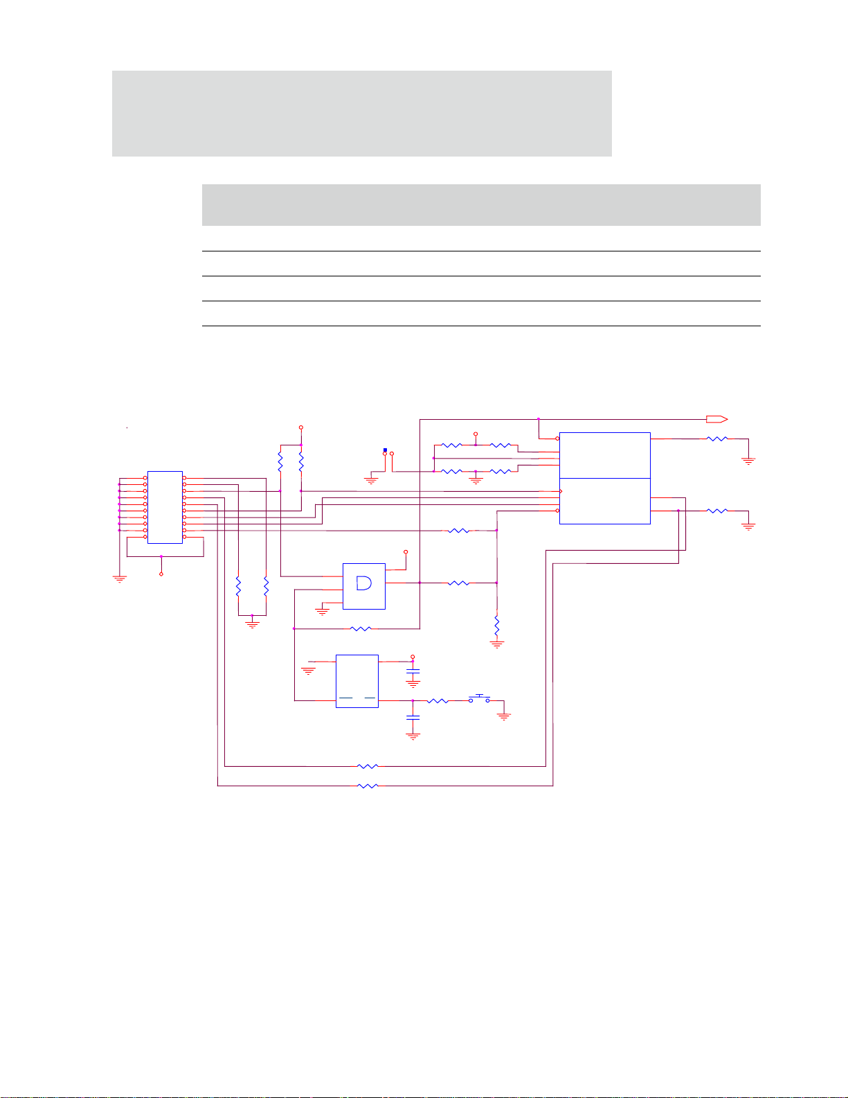
Pinout and signal descriptions
TRSTn
R15 0
**
**
R4
33
R13
10K
PD_PIN19
TCK
**
3.3V
3.3V
RTCK
##
TDI
U2
NC7SZ08_SOT23
1
2
3
5
4
A
B
GND
VCC
Y
RSTn
JSRST
R9 2.4K
##
R7 10K
RESET monitor
Trip = 2.97V
R14
10K
JP1
R10 2.4K
R3
1.0K
##
JTDO
C3
.1
R2
10K
R16
0
R12
2.4K
JTAG 20
PIN
HEADER..
##
R5
33
TMS
3.3V
PD_PIN17
P1
HEADER 10X2.1SP
12
34
56
78
910
1112
1314
1516
1718
1920
R17
2.4K
SW1
SW_PB
SYSTEM CONTROL
JTAG
NS9750_BGA352
H25 AC21
AE20
AD18
AC18
AE19
AF20 AD19
AF21
AD20
AE21
RESET* RESET_DONE
TCK
TDI
TMS
TDO
TRST* RTCK
PLLTEST*
BISTEN*
SCANEN*
R6 10K
Should be
positioned on
PCB with pin 1
facing toward
board edge.
R8
2.4K
3.3V
RESETn
RESETn
JRTCK
U3
MAX811S_SOT143
1
2
4
3
GND
RST
+V
MR
**
R11 0
##
MRn
**
nTRST
TDO
**
C1
.001
R1
2.4K
JP1 recommended
instead of R9
during development
3.3V
phase,
NS9750
Notes
R8
out: Boot from flash/ROM/S_CS1n
in: Boot from SDRAM/CS0n using SPI_B
EEPROM on GPIO pins
R12
out: Internal PCI arbiter
in: External PCI arbiter bus
Debug
Load all except JP1/R9, R15, R16; R8 and R12
depend on board options
Disable blank or unprogrammed boot memory
Production with debug possibility
Omit parts with **
Production without debug possibility
Omit parts with ** and ##, as well as parts with **
When halting the CPU in debug mode, the
JSRST line must be pulsed low only one time.
Bits Signal name U/D
AE19 tdo 2 O Test data out
AC18 tms U I Test mode select
AF20 trst_n U I Test mode reset
AD19 rtck U 2 I/O Returned test clock, ARM core only
Table 14: JTAG interface/boundary scan pinout
OD
(mA)
I/O Description
44
Figure 9: JTAG interface
NS9750 Hardware Reference
Page 69

Reserved
NS9750 Pinout
Pin# Description
J1 Tie to ground directly
K3 Tie to ground directly
K2 Tie to ground directly
K1 Tie to ground directly
R1 Tie to ground directly
R2 Tie to ground directly
R3 Tie to ground directly
T1 Tie to ground directly
AF6 Tie to ground directly
AE3 Tie to ground directly
AC5 Tie to ground directly
AD4 Tie to 1.5V core power
AF2 Tie to 3.3V I/O power
AE7 No connect
L3 No connect
L2 No connect
L1 No connect
M3 No connect
M2 Tie to ground directly
M1 Tie to ground directly
N1 Tie to ground directly
N2 Tie to ground directly
AF22 No connect
AD21 No connect
AE22 No connect
Table 15: Reserved pins
www.digiembedded.com
45
Page 70

Pinout and signal descriptions
Power ground
Pin # Signal name Description
J23, L23, K23, U23, T23, V23, D18,
D17, AC17, D16, AC16, D11, D10,
AC11, AC10, AC9, J4, L4, K4, U4,
T4, V4
G23, H23, M23, R23, P23, N23, Y23,
W23, D20, AC20, D19, AC19, D14,
D13, AC14, AC13, D8, D7, AC8,
AC7, G4, H4, M4, R4, P4, N4, Y4,
W4
A26, B25, AE25, AF26, D23, C24,
AD24, AC23, D5, D4, C4, E4, AC4,
A3, A2, D3, C3, C2, B3, B2, AE2,
AD3, A1, C1, B1, AF1
Table 16: Power ground pins
VDDC Core power, 1.5V
VDDS I/O power, 3.3V
VSS2 Ground
46
NS9750 Hardware Reference
Page 71

Working with the CPU
CHAPTER 3
The NS9750 core is based on the ARM926EJ-S processor. The ARM926EJ-S processor
belongs to the ARM9 family of general-purpose microprocessors. The ARM926EJ-S
processor is targeted at multi-tasking applications in which full memory
management, high performance, low die size, and low power are important.
47
Page 72

About the processor
About the processor
The ARM926EJ-S processor supports the 32-bit ARM and 16-bit Thumb instructions
sets, allowing you to trade off between high performance and high code density. The
processor includes features for efficient execution of Java byte codes, providing Java
performance similar to JIT but without the assoc iated overhead.
The ARM926EJ-S supports the ARM debug architecture, and includes logic to assist in
both hardware and software debug. The processor has a Harvard-cached architecture
and provides a complete high-performance processor subsystem, including:
ARM926EJ-S integer core
Memory Management Unit (MMU) (see "Memory Management Unit (MMU),"
beginning on page 78, for information)
Separate instruction and data AMBA AHB bus interfaces
48
NS9750 Hardware Reference
Page 73

Figure 10 shows the main blocks in the ARM926EJ-S processor.
DEXT
Write buffer
DCACHE
Cache
PA
TAGRAM
writeback
write
buffer
MMU
TLB
ARM926EJ-S
IROUTE
DROUTE
FCSE
WDATA RDATA
INSTR
ICACHE
IEXT
Bus
interface
unit
Data
AHB
interface
Instruction
AHB
interface
AHB
AHB
DA
IA
DMVA
IMVA
Working with the CPU
Figure 10: ARM926EJ-S processor block diagram
Instruction sets
The processor executes three instruction sets:
32-bit ARM instruction set
16-bit Thumb instruction set
8-bit Java instruction set
www.digiembedded.com
49
Page 74

Instruction sets
ARM instruction set
The ARM instruction set allows a program to achieve maximum performance with the
minimum number of instructions. The majority of instructions are executed in a
single cycle.
Thumb instruction set
The Thumb instruction set is simpler than the ARM instruction set, and offers
increased code density for code that does not require maximum performance. Code
can switch between ARM and Thumb instruction sets on any procedure call.
Java instruction set
In Java state, the processor core executes a majority of Java bytecodes naturally.
Bytecodes are decoded in two states, compared to a single decode stage when in
ARM/Thumb mode. See "Jazelle (Java)" on page 77 for more information about Java.
50
NS9750 Hardware Reference
Page 75

System control processor (CP15) registers
The system control processor (CP15) registers configure and control most of the
options in the ARM926EJ-S processor. Access the CP15 registers using only the MRC
and MCR instructions in a privileged mode; the instructions are provided in the
explanation of each applicable register. Using other instructions, or MRC and MCR in
unprivileged mode, results in an UNDEFINED instruction exception.
ARM926EJ-S system addresses
The ARM926EJ-S has three distinct types of addresses:
In the ARM926EJ-S domain: Virtual address (VA)
In the Cache and MMU domain: Modified virtual address (MVA)
In the AMBA domain: Physical address (PA)
Example
Working with the CPU
This is an example of the address manipulation that occurs when the ARM926EJ-S
core requests an instruction:
1 The ARM926EJ-S core issues the virtual address of the instruction.
2 The virtual address is translated using the FCSE PID (fast context switch
extension process ID) value to the modified virtual address. The instruction
cache (ICache) and memory management unit (MMU) find the modified virtual
address (see "R13: Process ID register" on page 75).
3 If the protection check carried out by the MMU on the modified virtual address
does not abort and the modified virtual address tag is in the ICache, the
instruction data is returned to the ARM926EJ-S core.
If the protection check carried out by the MMU on the modified virtual
address does not abort but the cache misses (the MVA tag is not in the
cache), the MMU translates the modified virtual address to produce the
physical address. This address is given to the AMBA bus interface to perform
an external access.
www.digiembedded.com
51
Page 76

System control processor (CP15) registers
Cond
1110 1111 1L
Opcode
_1
Opcode
_2
CRn CRmRd
31 28 27 26 25 24 23 21 20 19 16 15 12 11 10 9 8 7 5 4 3 0
Accessing CP15 registers
Use only MRC and MCR instructions, only in privileged mode, to access CP15 registers.
Figure 11 shows the MRC and MCR instruction bit pattern.
Figure 11: CP15 MRC and MCR bit pattern
The mnemonics for these instructions are:
MCR{cond} p15,opcode_1,Rd,CRn,CRm,opcode_2
MRC{cond} p15,opcode_1,Rd,CRn,CRm,opcode_2
If you try to read from a write-only register or write to a read-only register, you will
UNPREDICTABLE results. In all instructions that access CP15:
have
The opcode_1 field SHOULD BE ZER O, except when the values specified are used
to select the operations you want. Using other values results in
unpredictable behavior.
The opcode_2 and CRm fields SHOULD BE ZERO, except when the values
specified are used to select the behavior you want. Using other values
results in unpredictable behavior.
Terms and abbreviations
Table 17 lists the terms and abbreviations used in the CP15 registers and
explanations.
Term Abbreviation Description
UNPREDICTABLE UNP For reads:
Table 17: CP15 terms and abbreviations
52
NS9750 Hardware Reference
The data returned when reading from this location is
unpredictable, and can have any value.
For writes:
Writing to this location causes unpredictable
behavior, or an unpredictable change in device
configuration.
Page 77

Working with the CPU
Term Abbreviation Description
UNDEFINED UND An instruction that accesses CP15 in the manner
indicated takes the UNDEFINED instruction exception.
SHOULD BE ZERO SBZ When writing to this field, all bits of the field SHOULD
BE ZERO
SHOULD BE ONE SBO When writing to this location, all bits in this field
SHOULD BE ONE.
.
SHOULD BE ZERO or
PRESERVED
Table 17: CP15 terms and abbreviations
Note:
Register summary
CP15 uses 16 registers.
Register locations 0, 5, and 13 each provide access to more than one
register. The register accessed depends on the value of the
the CP15
Register location 9 provides access to more than one register. The register
accessed depends on the value of the
registers" on page 52).
SBZP When writing to this location, all bits of this field
SHOULD BE ZERO or PRESERVED by writing the
same value that has been read previously from the
same field.
In all cases, reading from or writing any data values to any CP15 registers,
including those fields specified as
SHOULD BE ZERO, does not cause any physical damage to the chip.
MRC/MCR instructions (see "Accessing CP15 registers" on page 52).
UNPREDICTABLE, SHOULD BE ONE, or
opcode_2 field in
CRm field (see "Accessing CP15
Register Reads Writes
0 ID code (based on
0 Cache type (based on opcode_2 value) Unpredictable
1 Control Control
2 Translation table base Translation table base
3 Domain access control Domain access control
opcode_2 value) Unpredictable
Table 18: CP15 register summary
www.digiembedded.com
53
Page 78

System control processor (CP15) registers
Register Reads Writes
4 Reserved Reserved
5 Data fault status (based on opcode_2 value) Data fault status (based on opcode_2 value)
6 Instruction fault status (based on opcode_2
value)
Instruction fault status (based on opcode_2
value)
7 Cache operations Cache operations
8 Unpredictable TLB
9 Cache lockdown (based on
CRm value) Cache lockdown
10 TLB lockdown TLB lockdown
11 and 12 Reserved Reserved
13 FCSE PID (based on
FCSE = Fast context switch extension
PID = Process identifier
13 Context ID (based on
opcode_2 value)
FCSE PID (based on
opcode_2 value)
FCSE = Fast context switch extension
PID = Process identifier
opcode_2 value) Context ID (based on opcode_2 value)
14 Reserved Reserved
15 Test configuration Test configuration
Table 18: CP15 register summary
All CP15 register bits that are defined and contain state are set to 0 by reset, with
these exceptions:
The V bit is set to 0 at reset if the VINITHI signal is low, and set to 1 if the
VINITHI signal is high.
54
The B bit is set to 0 at reset if the BIGENDINIT signal is low, and set to 1 if the
BIGENDINIT signal is high.
NS9750 Hardware Reference
Page 79

R0: ID code and cache type status registers
Register R0 access the ID register, and cache type register. Reading from R0 returns
the device ID, and the cache type, depending on the
opcode_2=0 ID value
opcode_2=1 instruction and data cache type
The
CRm field SHOULD BE ZERO when reading from these registers. Table 19 shows the
instructions you can use to read register R0.
Function Instruction
Working with the CPU
opcode_2 value:
Read ID code
Read cache type
MRC p15,0,Rd,c0,c0,{0, 3-7}
MRC p15,0,Rd,c0,c0,1
Table 19: Reading from register R0
Writing to register R0 is
UNPREDICTABLE.
R0: ID code
R0: ID code is a read-only register that returns the 32-bit device ID code. You can
access the ID code register by reading CP15 register R0 with the
opcode_2 field set to
any value other than 1 or 2. Note this example:
MRC p15, 0, Rd, c0, c0, {0, 3-7}; returns ID
Table 20 shows the contents of the ID code register.
Bits Function Value
[31:24] ASCII code of implementer trademark 0x41
[23:20] Specification revision 0x0
[19:16] Architecture (ARMv5TEJ) 0x6
[15:4] Part number 0x926
[3:0] Layout revision 0x0
Table 20: R0: ID code
www.digiembedded.com
55
Page 80

System control processor (CP15) registers
Ctype
0S
Dsize
31 28 25 24 23 12
00
Isize
R0: Cache type register
R0: Cache type is a read-only register that contains information about the size and
architecture of the instruction cache (ICache) and data cache (DCache) enabling
operating systems to establish how to perform operations such as cache cleaning and
lockdown. See "Cache features" on page 105 for more information about cache.
You can access the cache type register by reading CP1 5 register R0 with the
opcode_2
field set to 1. Note this example:
MRC p15, 0, Rd, c0, c0, 1; returns cache details
Figure 12 shows the format of the cache type register. Table 21 describes the fields in
the register.
Figure 12: Cache type register format
Field Description
Ctype Determines the cache type, and specifies whether the cache supports lockdown and how it is
cleaned. Ctype encoding is shown below; all unused values are reserved.
Value: 0b1110
Method: Writeback
Cache cleaning: Register 7 operations (see "R7: Cache Operations register" on page 64)
Cache lockdown: Format C (see "R9: Cache Lockdown register" on page 69)
S bit Specifies whether the cache is a unified cache (S=0) or separate ICache and DCache (S=1).
Will always report separate ICache and DCache for NS9750.
Dsize Specifies the size, line length, and associativity of the DCache.
Isize Species the size, length and associativity of the ICache.
Table 21: Cache type register field definition
56
NS9750 Hardware Reference
Page 81

Working with the CPU
11 10 9 6 5 3 2 1 0
00 Size MAssoc Len
Dsize and Isize fields
The Dsize and Isize fields in the cache type register have the same format, as shown:
The field contains these bits:
Field Description
Size Determines the cache size in conjunction with the M bit.
The M bit is 0 for DCache and ICache.
The size field is bits [21:18] for the DCache and bits [9:6] for the ICache.
The minimum size of each cache is 4 KB; the maximum size is 128 KB.
Cache size encoding with M=0:
Size field Cache size
0b0011 4 KB
0b0100 8 KB
Note: The NS9750 always reports 4KB for DCache and 8KB for ICache.
Assoc Determines the cache associativity in conjunction with the M bit.
The M bit is 0 for both DCache and ICache.
The assoc field is bits [17:15 for the DCache and bits [5:3] for the ICache.
Cache associativity with encoding:
Assoc field Associativity
0b010 4-way
Other values Reserved
M bit Multiplie r bit. Determines the cache size and cache associativity values in conjunction with the
size and assoc fields.
Note: This field must be set to 0 for the ARM926EJ-S processor.
Len Determines the line length of the cache.
The len field is bits [13:12] for the DCache and bits [1:0] for the ICache.
Line length encoding:
Len field Cache line length
10 8 words (32 bytes)
Other values Reserved
www.digiembedded.com
57
Page 82

System control processor (CP15) registers
131 19 16 15 12 11 10 9 8 7 3 0218 17 14 13 6
S
B
Z
SBZ
S
B
O
S
B
O
L4R
R
VI
SBZ
RSB
SBO
CAM
R1: Control register
Register R1 is the control register for the ARM926EJ-S processor. This register
specifies the configuration used to enable and disable the caches and MMU (memory
management unit). It is recommended that you access this register using a readmodify-write sequence.
For both reading and writing, the
CRm and opcode_2 fields SHOULD BE ZERO. Use these
instructions to read and write this register:
MRC p15, 0, Rd, c1, c0, 0 ; read control register
MCR p15, Rd, c1, c0, 0 ; write control register
All defined control bits are set to zero on reset except the V bit and B bit.
The V bit is set to zero at reset if the VINITHI signal is low.
The B bit is set to zero at reset if the BIGENDINIT signal is low , and set to one
BIGENDINIT signal is high.
if the
Figure 13 shows the Control register format. Table 22 describes the Control register
bit functionality.
Figure 13: Control register format
Bits Name Function
[31:19] N/A Reserved:
When read, returns an UNPREDICTABLE value.
When written, SHOULD BE ZERO, or a value read from bits
[31:19] on the same processor.
Use a read-modify-write sequence when modifying this
register to provide the greatest future compatibility.
58
[18] N/A Reserved, SBO. Read = 1, write =1.
[17] N/A Reserved, SBZ. read = 0, write = 0.
[16] N/A Reserved, SBO. Read = 1, write = 1.
Table 22: R1: Control register bit definition
NS9750 Hardware Reference
Page 83

Working with the CPU
Bits Name Function
[15] L4 Determines whether the T is set when load instructions change
the PC.
0 Loads to PC set the T bit
1 Loads to PC do not set the T bit
[14] RR bit Replacement strategy for ICache and DCache
0 Random replacement
1 Round-robin replacement
[13] V bit Location of exception vectors
0 Normal exception vectors selected; address range=
0000
to 0x0000 001C
0x0000
1 High exception vectors selected; address range=0xFFFF
0000
to 0xFFFF 001C
Set to the value of VINITHI on reset.
[12] I bit ICache enable/disable
0 ICache disabled
1 ICache enabled
[11:10] N/A
SHOULD BE ZERO
[9] R bit ROM protection
Modifies the ROM protection system.
[8] S bit System protection
Modifies the MMU protection system. See "Memory
Management Unit (MMU)," beginning on page 78.
[7] B bit Endianness
0 Little endian operation
1 Big endian operation
Set to the value of
BIGENDINIT on reset.
[6:3] N/A Reserved. SHOULD BE ONE.
[2] C bit DCache enable/disable
0 Cache disabled
1 Cache enabled
[1] A bit Alignment fault enable/disable
0 Data address alignment fault checking disabled
1 Data address alignment fault checking enabled
Table 22: R1: Control register bit definition
www.digiembedded.com
59
Page 84

System control processor (CP15) registers
Bits Name Function
[0] M bit MMU enable/disable
Table 22: R1: Control register bit definition
The M, C, I, and RR bits directly affect ICache and DCache behavior, as shown:
Cache MMU Behavior
ICache disabled Enabled or disabled All instruction fetches are from external memory (AHB).
ICache enabled Disabled All instruction fetches are cachable, with no protection
ICache enabled Enabled Instruction fetches are cachable or noncachable, and
0 Disabled
1Enabled
checking. All addresses are flat-mapped; that is:
VA=MVA=PA.
protection checks are performed. All addresses are
remapped from VA to PA, depending on the MMU page
table entry; that is, VA translated to MVA, MVA
remapped to PA.
60
DCache disabled Enabled or disabled All data accesses are to external memory (AHB).
DCache enabled Disabled All data accesses are noncachable nonbufferable. All
addresses are flat-mapped; that is, VA=MVA=PA.
DCache enabled Enabled All data accesses are cachable or noncachable, and
protection checks are performed. All addresses are
remapped from VA to PA, depending on the MMU page
table entry; that is, VA translated to MVA, MVA
remapped to PA.
Table 23: Effects of Control register on caches
If either the DCache or ICache is disabled, the contents of that cache are not
accessed. If the cache subsequently is re-enabled, the contents will not have
changed. To guarantee that memory coherency is maintained, the DCache must be
cleaned of dirty data before it is disabled.
NS9750 Hardware Reference
Page 85

R2: Translation Ta ble Base register
31 014 13
Translation table base
UNP/SBZ
31 014 13 12 11 10 9 8 7 6 5 4 3 2 115161718192021222324252627282930
D0D1D2D3D4D5D6D7D8D9D10D11D12D13D14D15
Register R2 is the Translation Table Base register (TTBR), for the base address of the
first-level translation table.
Reading from R2 returns the pointer to the currently active first-level
translation table in bits [31:14] and an
Writing to R2 updates the pointer to the first-level translation table from
the value in bits[31:14] of the written value. Bits [13:0]
Use these instructions to access the Translation Table Base register:
MRC p15, 0, Rd, c2, c0, 0 ; read TTBR
MCR p15, 0, Rd, c2, c0, 0 ; write TTBR
The CRm and opcode_2 fields SHOULD BE ZERO when writing to R2.
Figure 14 shows the format of the Translation Table Base register.
Figure 14: R2: Translation Table Base register
Working with the CPU
UNPREDICTABLE value in bits [13:0].
SHOULD BE ZERO.
R3: Domain Access Control register
Register R3 is the Domain Access Control register and consists of 16 two-bit fields, as
shown in Figure 15.
Figure 15: R3: Domain Access Control register
Reading from R3 returns the value of the Domain Access Control register.
Writing to R3 writes the value of the Domain Access Control register.
www.digiembedded.com
61
Page 86

System control processor (CP15) registers
Each two-bit field defines the access permissions for one of the 16 domains (D15–D0):
00 No access: Any access generates a domain fault
01 Client: Accesses are checked against the access permission bits in the section or page descriptor
10 Reserved: Currently behaves like no access mode (00)
11 Manager: Accesses are not checked against the access permission bits, so a permission fault
cannot be generated.
Use these instructions to access the Domain Access Control register:
MRC p15, 0, Rd, c3, c0, 0 ; read domain access permissions
MCR p15, 0, Rd, c3, c0, 0 ; write domain access permissions
R4 register
Accessing (reading or writing) this register causes UNPREDICTABLE behavior.
R5: Fault Status registers
Register R5 accesses the Fault Status registers (FSRs). The Fault Status registers
contain the source of the last instruction or data fault. The instruction-side FSR is
intended for debug purposes only.
62
The FSR is updated for alignment faults and for external aborts that occur while the
MMU is disabled. The FSR accessed is determined by the
opcode_2=0 Data Fault Status register (DFSR)
opcode_2=1 Instruction Fault Status register (IFSR)
opcode_2 value:
See "Memory Management Unit (MMU)," beginning on page 78, for the fault type
encoding.
Access the FSRs using these instructions:
MRC p15, 0, Rd, c5, c0, 0 ; read DFSR
MCR p15, 0, Rd, c5, c0, 0 ; write DFSR
MRC p15, 0, Rd, c5, c0, 1 ; read IFSR
MCR p15, 0, Rd, c5, c0, 1 ; write IFSR
NS9750 Hardware Reference
Page 87

Working with the CPU
31 0987 43
0
UNP/SBZ Domain Status
Figure 16 shows the format of the Fault Status registers. Table 24 describes the Fault
Status register bits.
Figure 16: Fault Status registers format
Bits Description
[31:9]
UNPREDICTABLE/SHOULD BE ZERO
[8] Always reads as zero. Writes are ignored.
[7:4] Specifies which of the 16 domains (D15–D0) was being accessed when a data
fault occurred.
[3:0] Type of fault generated. (See "Memory Management Unit (MMU)," beginning
on page 78.)
Table 24: Fault Status register bit description
Table 25 shows the encodings used for the status field in the Fault Status register, and
indicates whether the domain field contains valid information. See "MMU faults and
CPU aborts" on page 95 for information about MMU aborts in Fault Address and Fault
Status registers.
Priority Source Size Status Domain
Highest Alignment N/A
External abort on translation First level
Second level
Translation Section page
0b00x1
0b1100
0b1110
0b0101
0b0111
Invalid
Invalid
Valid
Invalid
Valid
Domain Section page
Permission Section page
Table 25: Fault Status register status field encoding
www.digiembedded.com
0b1001
0b1011
0b1101
0b1111
Valid
Valid
Valid
Valid
63
Page 88

System control processor (CP15) registers
Priority Source Size Status Domain
Lowest External abort Section page
Table 25: Fault Status register status field encoding
R6: Fault Address register
Register R6 accesses the Fault Address register (FAR). The Fault Address register
contains the modified virtual address of the access attempted when a data abort
occurred. This register is updated only for data aborts, not for prefetch aborts; it is
updated also for alignment faults and external aborts that occur while the MMU is
disabled.
Use these instructions to access the Fault Address register:
MRC p15, 0, Rd, c6, c0, 0 ; read FAR
MCR p15, 0, Rd, c6, c0, 0 ; write FAR
Writing R6 sets the Fault Address register to the value of the data written. This is
useful for debugging, to restore the value of a Fault Address register to a previous
state.
CRm and opcode_2 fields SHOULD BE ZERO when reading or writing R6.
The
0b1000
0b1010
Valid
Valid
R7: Cache Operations register
Register R7 controls the caches and write buffer. The function of each cache
operation is selected by the
to CP15 R7. Writing other
Reading from R7 is UNPREDICTABLE, with the exception of the two test and clean
operations (see Table 27, “R7: Cache operations,” on page 66 and "Test and clean
operations" on page 67).
Use this instruction to write to the Cache Operations register:
MCR p15, opcode_1, Rd, CRn, CRm, opcode_2
Table 26 describes the cache functions provided by register R7. Table 27 lists the
cache operation functions and associated data and instruction formats for R7.
64
NS9750 Hardware Reference
opcode_2 and CRm fields in the MCR instruction that writes
opcode_2 or CRm values is UNPREDICTABLE.
Page 89

Working with the CPU
Function Description
Invalidate cache Invalidates all cache data, including any dirty data.
Invalidate single entry using either index or
Invalidates a single cache line, discarding any dirty data.
modified virtual address
Clean single data entry using either index or
modified virtual address
Writes the specified DCache line to main memory if the
line is marked valid and dirty. The line is marked as not
dirty, and the valid bit is unchanged.
Clean and invalidate single data entry using
wither index or modified virtual address.
Writes the specified DCache line to main memory if the
line is marked valid and dirty. The line is marked not valid.
Test and clean DCache Tests a number of cache lines, and cleans one of them if any
are dirty. Returns the overall dirty state of the cache in bit
30. (See "Test and clean operations" on page 67).
Test, clean, and invalidate DCache Tests a number of cache lines, and cleans one of them if any
are dirty. When the entire cache has been tested and
cleaned, it is invalidated. (See "Test and clean operations"
on page 67).
Prefetch ICache line Performs an ICache lookup of the specified modified
virtual address. If the cache misses and the region is
cachable, a linefill is performed.
Drain write buffer Acts as an explicit memory barrier. This instruction drains
the contents of the write buffers of all memory stores
occurring in program order before the instruction is
completed. No instructions occurring in program order
after this instruction are executed until the instruction
completes.
Use this instruction when timing of specific stores to the
level two memory system has to be controlled (for
example, when a store to an interrupt acknowledge location
has to complete before interrupts are enabled).
Table 26: Cache Operations register function descriptions
www.digiembedded.com
65
Page 90

System control processor (CP15) registers
Function Description
Wait for interrupt Drains the contents of the write buffers, puts the processor
Table 26: Cache Operations register function descriptions
Function/operation Data format Instruction
into low-power state, and stops the processor from
executing further instructions until an interrupt (or debug
request) occurs. When an interrupt does occur, the
MCR
instruction completes, and the IRQ or FIRQ handler is
entered as normal.
The return link in
MCR instruction plus eight, so the typical instruction
the
R14_irq or R14_fiq contains the address of
used for interrupt return (SUBS PC,R14,#4) returns to the
instruction following the
MCR.
Invalidate ICache and DCache SBZ
Invalidate ICache SBZ
Invalidate ICache single entry (MVA) MVA
Invalidate ICache single entry (set/way) Set/Way
Prefetch ICache line (MVA) MVA
Invalidate DCache SBZ
Invalidate DCache single entry (MVA) MVA
Invalidate DCache single entry (set/way) Set/Way
Clean DCache single entry (MVA) MVA
Clean DCache single entry (set/way) Set/Way
Test and clean DCache n/a
Clean and invalidate DCache entry (MVA) MVA
Clean and invalidate DCache entry (set/way) Set/Way
Test, clean, and invalidate DCache n/a
Drain write buffer SBZ
Wait for interrupt SBZ
MCR p15, 0, Rd, c7, c7, 0
MCR p15, 0, Rd, c7, c5, 0
MCR p15, 0, Rd, c7, c5, 1
MCR p15, 0, Rd, c7, c5, 2
MCR p15, 0, Rd, c7, c13, 1
MCR p15, 0, Rd, c7, c6, 0
MCR p15, 0, Rd, c7, c6, 1
MCR p15, 0, Rd, c7, c6, 2
MCR p15, 0, Rd, c7, c10, 1
MCR p15, 0, Rd, c7, C10, 2
MRC p15, 0, Rd, c7, c10, 3
MCR p15, 0, Rd, c7, c14, 1
MCR p15, 0, Rd, c7, c14, 2
MRC p15, 0, Rd, c7, c14, 3
MCR p15, 0, Rd, c7, c10, 4
MCR p15, 0, Rd, c7, c0, 4
66
Table 27: R7: Cache operations
NS9750 Hardware Reference
Page 91

Working with the CPU
31 0S+4 4
SBZSet(=index) Word
Tag
215S+5
31 0S+4 4
SBZSet(=index) Word
SBZ
215S+5
Way
32-A 31-A
Figure 17 shows the modified virtual address format for Rd for the CP15 R7 MCR
operations.
The tag, set, and word fields define the MVA.
For all cache operations, the word field SHOULD BE ZERO.
Figure 17: R7: MVA format
Figure 18 shows the Set/Way format for Rd for the CP15 R7 MCR operations.
A and S are the base-two logarithms of the associativity and the number of
sets.
The set, way, and word files define the format.
For all of the cache operations, word SHOULD BE ZERO.
For example, a 16 KB cache, 4-way set associative, 8-word line results in the
following:
A = log
S = log
associativity = log24 = 2
2
NSETS where
2
NSETS = cache size in bytes/associativity/line length in bytes:
NSETS = 16384/4/32 = 128
Result: S = log
128 = 7
2
Figure 18: R7: Set/Way format
Test and clean operations
Test and clean DCache instruction
The test and clean DCache instruction provides an efficient way to clean the entire
DCache, using a simple loop. The test and clean DCache instruction tests a number of
lines in the DCache to determine whether any of them are dirty. If any dirty lines are
www.digiembedded.com
67
Page 92

System control processor (CP15) registers
found, one of those lines is cleaned. The test and clean DCache instruction also
returns the status of the entire DCache in bit 30.
Note:
The test and clean DCache ins t ruction MRC p15, 0, r15, c7, c10, 3 is a special
encoding that uses
using this instruction, however. This
condition code flags.
If the cache contains any dirty lines, bit 30 is set to 0. If the cache contains no dirty
lines, bit 30 is set to 1. Use the following loop to clean the entire cache:
tc_loop: MRC p15, 0, r15, c7, c10, 3 ; test and clean
Test, clean, and invalidate DCache instruction
The test, clean, and invalidate DCache instruction is the same as the test and clean
DCache instruction except that when the entire cache has been cleaned, it is
invalidated. Use the following loop to test, clean, and invalidate the entire DCache:
tci_loop: MRC p15, 0, r15, c7, c14, 3 ; test clean and invalidate
R8:TLB Operations register
Register R8 is a write-only register that controls the translation lookaside buffer
(TLB). There is a single TLB used to hold entries for both data and instructions. The
TLB is divided into two parts:
r15 as a destination operand. The PC is not changed by
MRC instruction also sets the
BNE tc_loop
BNE tci_loop
68
Set-associative
Fully-associative
The fully-associative part (also referred to as the lockdown part of the TLB) stores
entries to be locked down. Entries held in the lockdown part of the register are
preserved during an invalidate-TLB operation. Entries can be removed from the
lockdown TLB using an invalidate TLB single entry operation.
There are six TLB operations; the function to be performed is selected by the
CRm fields in the MCR instruction used to write register R8. Writing other opcode_2
and
CRm values is UNPREDICTABLE. Reading from this register is UNPREDICTABLE.
or
opcode_2
Use the instruction shown in Table 28 to perform TLB operations.
NS9750 Hardware Reference
Page 93

Operation Data Instruction
31 09
SBZ
Modified virtual address
10
Working with the CPU
Invalidate set-associative TLB SBZ
Invalidate single entry SBZ
Invalidate set-associative TLB SBZ
Invalidate single entry MVA
Invalidate set-associative TLB SBZ
Invalidate single entry MVA
MCR p15, 0, Rd, c8, c7, 0
MCR p15, 0, Rd, c8, c7. 1
MCR p15, 0, Rd, c8, c5, 0
MCR p15, 0, Rd, c8, c5, 1
MCR p15, 0, Rd, c8, c6, 0
MCR p15, 0, Rd, c8, c6, 1
Table 28: R8: Translation Lookaside Buffer operations
The invalidate TLB operations invalidate all the unpreserved entries in the
TLB.
The invalidate TLB single entry operations invalidate any TLB entry
corresponding to the modified virtual address given in
Rd, regardless of its
preserved state. See "R10: TLB Lockdown register," beginning on page 73,
for an explanation of how to preserve TLB entries.
Figure 19 shows the modified virtual address format used for invalid TLB single entry
operations.
Figure 19: R8: TLB Operations, MVA format
Note:
If either small or large pages are used, and these pages contain subpage
access permissions that are different, you must use four invalidate TLB
single entry operations, with the MVA set to each subpage, to invalidate
all information related to that page held in a TLB.
R9: Cache Lockdown register
Register R9 access the cache lockdown registers. Access this register using CRm = 0.
The Cache Lockdown register uses a cache-way-based locking scheme (format C) that
allows you to control each cache way independently.
www.digiembedded.com
69
Page 94

System control processor (CP15) registers
These registers allow you to control which cache-ways of the four-way cache are used
for the allocation on a linefill. When the registers are defined, subsequent linefills
are placed only in the specified target cache way. This gives you some control over
the cache pollution cause by particular applications, and provides a traditional
lockdown operation for locking critical code into the cache.
A locking bit for each cache way determines wheth er the normal cache allocation is
allowed to access that cache way (see Table 30, “Cache Lockdown register L bits,” on
page 71). A maximum of three cache ways of the four-way associative cache can be
locked, ensuring that normal cache line replacement is performed.
Note:
If no cache ways have the L bit set to 0, cache way 3 is used for all
linefills.
The first four bits of this register determine the L bit for the associated cache way.
The opcode_2 field of the MRC or MCR instruction determines whether the instruction
or data lockdown register is accessed:
opcode_2=0 Selects the DCache Lockdown register, or the Unified
Cache Lockdown register if a unified cache is
implemented. The ARM926EJ-S processor has separate
DCache and ICache.
opcode_2=1 Selects the ICache Lockdown register.
Use the instructions shown in Table 29 to access the CacheLockdown register.
Function Data Instruction
Read DCache Lockdown register L bits
Write DCache Lockdown register L bits
Read ICache Lockdown register L bits
Write ICache Lockdown register L bits
MRC p15, 0, Rd, c9, c0, 0
MCR p15, 0, Rd, c9, c0, 0
MRC p15, 0, Rd, c9, c0, 1
MCR p15, 0, Rd, c9, c0, 1
70
Table 29: Cache Lockdown register instructions
You must modify the Cache Lockdown register using a modify-read-write sequence;
for example:
MRC p15, 0, Rn, c9, c0, 1 ;
ORR Rn, Rn, 0x01 ;
MCR p15, 0, Rn, c9, c0, 1 ;
NS9750 Hardware Reference
Page 95

Working with the CPU
31 03
SBZ/UNP
15 416
SB0
L bits
(cache ways
0 to 3)
This sequence sets the L bit to 1 for way 0 of the ICache. Figure 20 shows the format
for the Cache Lockdown register.
Figure 20: R9: Cache Lockdown register format
Table 30 shows the format of the Cache Lockdown register L bits. All cache ways are
available for allocation from reset.
Bits 4-way associative Notes
[31:16] UNP/SBZ Reserved
[15:4] 0xFFF SBO
[3] L bit for way 3 Bits [3:0] are the L bits for each cache way:
[2] L bit for way 2
[1] L bit for way 1
0 Allocation to the cache way is determined by the standard
replacement algorithm (reset state)
1 No allocation is performed to this way
[0] L bit for way 0
Table 30: Cache Lockdown register L bits
Use one of these procedures to lockdown and unlock cache:
Specific loading of addresses into a cache way
Cac he unlock procedure
www.digiembedded.com
71
Page 96

System control processor (CP15) registers
Specific loading of addresses into a cache-way
The procedure to lock down code and data into way i of cache, with N ways, using
format C, makes it impossible to allocate to any cache way other than the target
cache way:
1 Be sure that no processor exceptions can occur during the execution of this
procedure; for example, disable interrupts. If this is not possible, all code and
data used by any exception handlers must be treated as code and data as in
Steps 2 and 3.
2 If an ICache way is being locked down, be sure that all the code executed by the
lockdown procedure is in an uncachable area of memory or in an already locked
cache way.
3 If a DCache way is being locked down, be sure that all data used by the lockdown
procedure is in an uncachable area of memory or is in an already locked cache
way.
4 Ensure that the data/instructions that are to be locked down are in a cachable
area of memory.
5 Be sure that the data/instructions that are to be locked down are not already in
the cache. Use the Cache Operations register (R7) clean and/or invalidate
functions to ensure this.
72
6 Write these settings to the Cache Lockdown register (R9), to enable allocation to
the target cache way:
CRm = 0
Set L == 0 for bit i
Set L == 1 for all other bits
7 For each of the cache lines to be locked down in cache way i:
– If a DCache is being locked down, use an LDR instruction to load a word
from the memory cache line to ensure that the memory cache line is loaded
into the cache.
– If an ICache is being locked down, use the Cache Operations register (R7)
MCR prefetch ICache line (<CRm>==c13, <opcode2>==1) to fetch the memory
cache line into the cache.
8 Write <CRm>==0 to Cache Lockdown register (R9), setting L==1 for bit i and
restoring all other bits to the values they had before the lockdown routine was
started.
NS9750 Hardware Reference
Page 97

Cache unlock procedure
Victim SBZ/UNP
31 28 2529 26 0
SBZ P
To unlock the locked down portion of the cache, write to Cache Lockdown register
(R9) setting
L==0 for the appropriate bit. The following sequence, for example, sets
the L bit to 0 for way 0 of the ICache, unlocking way 0:
MRC p15, 0, Rn, c9, c0, 1;
BIC Rn, Rn, 0x01 ;
MCR p15, 0, Rn, c9, c0, 1;
R10: TLB Lockdown register
The TLB Lockdown register controls where hardware page table walks place the TLB
entry — in the set associative region or the lockdown region of the TLB. If the TLB
entry is put in the lockdown region, the register indicates which entry is written. The
TLB lockdown region contains eight entries (see the discussion of the TLB structure in
"TLB structure," beginning on page 104, for more information).
Figure 21 shows the TLB lockdown format.
Working with the CPU
Figure 21: TLB Lockdown register format
When writing the TLB Lockdown register, the value in the P bit (D0) determines in
which region the TLB entry is placed:
P=0 Subsequent hardware page table walks place the TLNB entry in the set associative region
of the TLB.
P=1 Subsequent hardware page table walks place the TLB entry in the lockdown region at the
entry specified by the victim, in the range 0–7.
TLB entries in the lockdown region are preserved so invalidate-TLB operations only
invalidate the unpreserved entries in the TLB; that is, those entries in the setassociative region. Invalidate-TLB single entry operations invalidate any TLB entry
corresponding to the modified virtual address given in
Rd, regardless of the entry’s
preserved state; that is, whether they are in lockdown or set-associative TLB regions.
www.digiembedded.com
73
Page 98

System control processor (CP15) registers
See "R8:TLB Operations register" on page 68 for a description of the TLB-invalidate
operations.
Use these instructions to program the TLB Lockdown register:
Function Instruction
Read data TLB lockdown victim
Write data TLB lockdown victim
MRC p15, 0, Rd, c10, c0, 0
MCR p15, 0, Rd, c10, c0, 0
The victim automatically increments after any table walk that results in an entry
being written into the lockdown part of the TLB.
Note:
It is not possible for a lockdown entry to map entirely either small or large
pages, unless all subpage access permissions are the same. Entries can
still be written into the lockdown region, but the address range that is
mapped covers only the subpage corresponding to the address that was
used to perform the page table walk.
Sample code sequence
This example shows the code sequence that locks down an entry to the current
victim.
ADR r1,LockAddr ; set R1 to the value of the address to be locked
down
MCR p15,0,r1,c8,c7,1 ; invalidate TLB single entry to ensure that
LockAddr is not already in the TLB
MRC p15,0,r0,c10,c0,0 ; read the lockdown register
ORR r0,r0,#1 ; set the preserve bit
MCR p15,0,r0,c10,c0,0 ; write to the lockdown register
LDR r1,[r1] ; TLB will miss, and entry will be loaded
MRC p15,0,r0,c10,c0,0 ; read the lockdown register (victim will have
; incremented
BIC r0,r0,#1 ; clear preserve bit
MCR p15,0,r0,c10,c0,0 ; write to the lockdown register
R11 and R12 registers
Accessing (reading or writing) these registers causes UNPREDICTABLE behavior.
74
NS9750 Hardware Reference
Page 99

R13: Process ID register
The Process ID register accesses the process identifier registers. The register
accessed depends on the value on the
opcode_2=0 Selects the Fast Context Switch Extension (FCSE) Process Identifier (PID)
opcode_2=1 Selects the context ID register.
Use the Process ID register to determine the process that is currently running. The
process identifier is set to 0 at reset.
FCSE PID register
Addresses issued by the ARM926EJ-S core, in the range 0 to 32 MB, are translated
according to the value contained in the FCSE PID register. Address A becomes
A + (FCSE PID x 32 MB); it is this modified address that the MMU and caches see.
Addresses above 32 MB are not modified. The FCSE PID is a 7-bit field, which allows
128 x 32 MB processes to be mapped.
Working with the CPU
opcode_2 field:
register.
If the FCSE PID is 0, there is a flat mapping between the virtual addresses output by
the ARM926EJ-S core and the modified virtual addresses used by the caches and MMU.
The FCSE PID is set to 0 at system reset.
If the MMU is disabled, there is no FCSE address translation.
FCSE translation is not applied for addresses used for entry-based cache or TLB
maintenance operations. For these operations,
VA=MVA.
Use these instructions to access the FCSE PID register:
Function Data ARM instruction
Read FCSE PID FCSE PID
Write FCSE PID FCSE PID
MRC p15,0,Rd,c13,c0,0
MCR p15,0,Rd,c13,c0,0
www.digiembedded.com
75
Page 100

System control processor (CP15) registers
31 25 24 0
SBZ
FCSE PID
Figure 22 shows the format of the FCSE PID register.
Figure 22: Process ID register format
Performing a fast context switch
You can perform a fast context switch by writing to the Process ID register (R13) with
opcode_2 set to 0. The contents of the caches and the TLB do not have to be flushed
after a fast context switch because they still hold address tags. The two instructions
after the FCSE PID has been written have been fetched with the old FCSE PID, as
shown in this code example:
{FCSE PID = 0}
MOV r0, #1:SHL:25 ;Fetched with FCSE PID = 0
MCR p15,0,r0,c13,c0,0 ;Fetched with FCSE PID = 0
A1 ;Fetched with FCSE PID = 0
A2 ;Fetched with FCSE PID = 0
A3 ;Fetched with FCSE PID = 1
76
A1, A2, and A3 are the three instructions following the fast context switch.
Context ID register
The Context ID register provides a mechanism that allows real-time trace tools to
identify the currently executing process in multi-tasking environments.
Use these instructions to access the Context ID register:
Function Data ARM instruction
Read context ID Context ID
Write context ID Context ID
NS9750 Hardware Reference
MRC p15,0,Rd,c13,c0,1
MCR p15,0,Rd,c13,c0,1
 Loading...