

Page 1

NS7520 Hardware Reference
90000353_D
Page 2

Page 3

NS7520 Hardware Reference
Part number/version: 90000353_D
Release date: March 2006
www.digi.com
Page 4

©2001-2006 Digi International Inc.
Printed in the United States of America. All rights reserved.
Digi, Digi International, the Digi logo, the Making Device Networking Easy logo, NetSilicon, a Digi
International Company, NET+, NET+OS and NET+Works are trademarks or registered trademarks of Digi
International, Inc. in the United States and other countries worldwide. All other trademarks are the
property of their respective owners.
Information in this document is subject to change without notice and does not represent a committment
on the part of Digi International.
Digi provides this document “as is,” without warranty of any kind, either expressed or implied, including,
but not limited to, the implied warranties of, fitness or merchantability for a particular purpose. Digi may
make improvements and/or changes in this manual or in the product(s) and/or the program(s) described
in this manual at any time.
This product could include technical inaccuracies or typographical errors. Changes are made periodically
to the information herein; these changes may be incorporated in new editions of the publication.
Digi International
11001 Bren Road East
Minnetonka, MN 55343 U.S.A.
United States: +1 877 912-3444
Other locations: +1 952 912-3444
www.digi.com/support/
www.digi.com
Page 5

Contents
Chapter 1: About the NS7520..................................................1
NS7520 Features ......................................................................... 2
Key features and operating modes of the major NS7520 modules........ 2
NS7520 module block diagram......................................................... 5
Operating frequency .................................................................... 6
Chapter 2:
Packaging ................................................................................. 8
Pinout detail tables and signal descriptions........................................11
Chapter 3:
ARM Thumb concept ...................................................................30
CPU performance.......................................................................30
Working with ARM exceptions ........................................................31
Pinout and Packaging ............................................7
System bus interface............................................................12
Chip select controller........................................................... 16
Ethernet interface MAC................................ ........ ....... ....... ... 18
“No connect” pins ...............................................................21
General-purpose I/O ............................................................21
System clock and reset .........................................................24
System mode (test support)....................................................25
JTAG test (ARM debugger) .....................................................26
Power supply .....................................................................28
Working with the CPU......................................... 29
Summary of ARM exceptions ...................................................32
Exception priorities.............................................................. 32
iii
Page 6

Exception vector table.......................................................... 33
Detail of ARM exceptions....................................................... 34
Entering and exiting an exception (software action) ......................37
Hardware Interrupts....................................................................39
FIRQ and IRQ lines............................................................... 39
Interrupt controller.............................................................. 39
Interrupt sources................................................................. 40
Chapter 4:
BBus Module ...........................................................43
BBus masters and slaves...............................................................44
Cycles and BBus arbitration...........................................................44
Address decoding .......................................................................45
Chapter 5:
SYS Module.............................................................47
Signal description....................................................................... 48
JTAG support............................................................................48
ARM debug...............................................................................49
System clock generation (NS7520 clock module) .................................. 49
External oscillator vs. internal PLL circuit...................................49
NS7520 clock module block diagram.......................................... 50
Using the external oscillator.......................................................... 50
External oscillator mode hardware configuration ..........................51
Using the PLL circuit ...................................................................52
PLL mode hardware configuration ............................................ 52
Setting the PLL frequency.............................................................54
PLL Settings register: Setting the PLL frequency on bootup..............54
PLL Control register: Setting the PLL frequency with the PLL Control
register............................................................................ 57
Reset circuit sources...................................................................59
NS7520 bootstrap initialization....................................................... 60
iv
Chapter 6: GEN Module
.............................................................61
Module configuration................................................................... 62
GEN module hardware initialization.................................................62
GEN module registers ..................................................................63
Page 7

System Control register.........................................................63
System Status register ..........................................................68
Software Service register.......................................................70
Timer Control registers .........................................................70
Timer Status registers...........................................................73
PORTA Configuration register.................................................. 74
PORTC Configuration register.................................................. 77
Interrupts ................................................................................ 80
Interrupt controller registers ..................................................81
Chapter 7:
Memory Controller Module................................. 85
About the MEM module ................................................................86
MEM module hardware initialization................................................. 86
Pin configuration.................................................................86
MEM module configuration ............................................................88
Setting the chip select address range ........................................88
Memory Module Configuration register.......................................90
Chip Select Base Address register.............................................93
Chip Select Option Register A ................................................. 97
Chip Select Option Register B.................................................101
Static memory (SRAM) controller ...................................................102
Single cycle read/write........................................................103
Burst cycles......................................................................104
NS7520 DRAM address multiplexing.................................................105
Using the internal multiplexer................................................105
Using the external multiplexer...............................................108
DRAM refresh...........................................................................109
FP/EDO DRAM controller .............................................................109
Single cycle read/write........................................................110
FP/EDO DRAM burst cycles ....................................................111
SDRAM ...................................................................................111
NS7520 SDRAM interconnect .................................. ....... ....... .. 1 12
SDRAM A10/AP support ........................................................116
Command definitions...........................................................117
Memory timing fields — SDRAM ...............................................118
BSIZE configuration.............................. ....... ........ ....... ....... .. 1 18
SDRAM Mode register..................... ....... ....... ........ ....... ....... .. 1 19
v
Page 8

SDRAM read cycles.............................................................. 1 20
SDRAM write cycles............................................... ....... .......122
Peripheral page burst size ...........................................................124
Chapter 8:
DMA Module.......................................................... 127
DMA module ............................................................................128
Fly-by operation transfers.....................................................128
Memory-to-memory operation................................................129
DMA buffer descriptor ................................................................130
DMA channel assignments ............................................................133
DMA channel registers ................................................................134
Address map.....................................................................134
Buffer Descriptor Pointer register ...........................................136
DMA Control register ........ ........ ....... ....... ........ ....... ....... ....... 1 36
DMA Status/Interrupt Enable register .......................................142
Ethernet transmitter considerations................................................144
Ethernet receiver considerations ...................................................145
External peripheral DMA support....................................................145
Signal description...............................................................146
External DMA configuration ...................................................146
Memory-to-memory mode.....................................................146
DMA controller reset ..................................................................147
Chapter 9:
Ethernet Module .................................................. 149
Ethernet front-end (EFE) .............................................................150
Transmit and receive FIFOs ...................................................151
EFE transmit processing .......................................................151
EFE receive processing.........................................................151
Receive buffer descriptor selection .........................................152
External CAM filtering ................................................................153
MAC module ............................................................................154
MAC module block diagram ...................................................154
DMA channel assignments ............................................................156
EFE configuration......................................................................156
Ethernet General Control register (EGCR) bit definitions ................158
Ethernet General Status register (EGSR) bit definitions..................164
vi
Page 9

Ethernet FIFO Data register...................................................167
Ethernet Transmit Status register............................................169
Ethernet Receive Status register.............................................174
MAC Configuration Register 1.................................................178
MAC Configuration Register 2.................................................180
Back-to-Back Inter-Packet-Gap register.....................................184
Non-Back-to-Back Inter-Packet-Gap register...............................185
Collision Window/Collision Retry register ..................................186
Maximum Frame register ......................................................187
PHY Support register...........................................................188
Test register.....................................................................189
MII Management Configuration register .....................................191
MII Management Command register..........................................193
MII Management Address register ............................................194
MII Management Write Data register ........................................195
MII Management Read Data register .........................................196
MII Management Indicators register..........................................197
SMII Status register .............................................................198
Station Address registers ......................................................198
Station Address Filter register................................................201
Register hash table.............................................................202
Chapter 10:
Serial Controller Module .................................209
Supported features....................................................................210
Bit-rate generator .....................................................................211
Serial protocols ........................................................................212
UART mode .............................................................................212
SPI mode ................................................................................213
FIFO management ................ ........ ....... ....... ........ ....... ....... .. 2 14
General-purpose I/O configurations ................................................222
Serial port performance..............................................................223
Configuration...........................................................................223
Serial Channel registers ..............................................................225
Serial Channel 1, 2 Control Register A ......................................225
Serial Channel 1, 2 Control Register B ......................................231
Serial Channel 1, 2 Status Register A........................................235
Serial Channel 1, 2 Bit-Rate registers .......................................244
vii
Page 10

Serial Channel 1, 2 FIFO registers............................................254
Serial Channel 1, 2 Receive Buffer Gap Timer .............................255
Serial Channel 1, 2 Receive Character Gap Timer.........................256
Serial Channel 1,2 Receive Match register..................................258
Serial Channel 1, 2 Receive Match MASK register..........................258
Chapter 11:
Electrical Characteristics............................... 261
DC characteristics .....................................................................262
Recommended operating conditions.........................................262
Input/Output characteristics .................................................263
Pad pullup and pulldown characteristics....................................263
Absolute maximum ratings ....................................................265
AC characteristics .....................................................................265
AC electrical specifications ...................................................265
Oscillator Characteristics...................................................... .......267
Timing Diagrams ................................... ....... ........ ....... ....... .......269
Timing_Specifications............... ...........................................269
Reset_timing ....................................................................270
SRAM timing .....................................................................271
SDRAM timing....................................................................281
FP DRAM timing .................................................................289
Ethernet timing .................................................................296
JTAG timing......................................................................298
External DMA timing............................................................300
Serial internal/external timing...............................................303
GPIO timing......................................................................305
viii
Index
Page 11

Using This Guide
Using This Guide
Review this section for basic information about the guide you are using, as
well as general support and contact information.
About this guide
This guide provides information about the NS7520 32-bit networked
microprocessor. The NS7520 is part of the NET+ARM line of SoC (System-onChip) products, and supports high-bandwidth applications for intelligent
networked devices.
The NET+ARM family is part of the NET+Works integrated product family, which
includes the NET+OS network software suite.
Who should read this guide
This guide is for hardware developers, system software developers, and
applications programmers who want to use the NS7520 for development.
To complete the tasks described in this guide, you must:
Understand the basics of hardware and software design, operating
systems, and microprocessor design.
Understand the NS7520 architecture.
ix
Page 12

What’s in this guide
This table shows where you can find specific information in this guide:
To read about See
NS7520 key features Chapter 1, "About the NS7520"
NS7520 ball grid array assignments & packaging Chapter 2, "Pinout and Packaging"
NS7520 CPU and ARM Thumb concept Chapter 3, "Working with the CPU"
BBus functionality Chapter 4, "BBus Module"
System functionality Chapter 5, "SYS Module"
General (GEN) module functionality Chapter 6, "GEN Module"
How the NS7520 can be configured to interface
with different types of memory devices
DMA controller, supported DMA channels, and
internal and external DMA transfers
Ethernet controller module Chapter 9, "Ethernet Module"
Serial channels A and B Chapter 10, "Serial Controller Module"
NS7520 timing information and diagrams Chapter 11, "Electrical Characteristics"
Conventions used in this guide
This table describes the typographic conventions used in this guide:
This convention Is used for
italic type Emphasis, new terms, variables, and document titles.
monospaced type
_ (underscore) Defines a signal as being active low.
‘b Indicates that the number following this indicator is in binary radix
Filenames, pathnames, and code examples.
Chapter 7, "Memory Controller Module"
Chapter 8, "DMA Module"
‘d Indicates that the number following this indicator is in decimal radix
‘h Indicates that the number following this indicator is in hexadecimal radix
x
NS7520 Hardware Reference, Rev. D 03/2006
Page 13

Related documentation
NS7520 Jumpers and Components provides a hardware description of the NET+Works
Development Board, and includes information about jumpers, connectors, switches,
and interface configurations, as well as development board diagrams.
Review the documentation CD-ROM that came with your development kit for
information on third-party products and other components.
See the NET+OS software documentation for information appropriate to the chi p you
are using.
Documentation updates
Digi occasionally provides documentation updates on the Web site
(www.digi.com/support).
Be aware that if you see differences between the documentation you received in your
package and the documentation on the Web site, the Web site content is the latest
version.
Customer support
To get help with a question or technical problem with this product, or to make
comments and recommendations about our products or documentation, use the
contact information listed in this table:
For Contact information
Technical support United States: +1 877 912-3444
Other locations: +1 952 912-3444
www.digi.com/support
www.digi.com
www.digi.com
xi
Page 14

Page 15

About the NS7520
CHAPTER 1
This chapter provides an overview of the NS7520. The NS7520 is a high-
performance, highly integrated, 32-bit system-on-a-chip ASIC designed for use in
intelligent networked devices and Internet appliances. The NS7520 is based on the
standard architecture in the NET+ARM family of devices.
NET+ARM is the hardware foundation of the NET+Works family of integrated hardware
and software solutions for device networking. These comprehensive platforms
include drivers, popular operating systems, networking software, development tools,
APIs, and complete development boards.
1
Page 16

NS7520 Features
NS7520 Features
The NS7520 can support most any networking scenario, and includes a 10/100 BaseT
Ethernet MAC and two independent serial ports (each of which can run in UART or SPI
mode).
The CPU is an ARM7TDMI (ARM7) 32-bit RISC processor core with a rich complement of
support peripherals and memory controllers, including:
Glueless connection to different types of memory; for example, flash,
SDRAM, EEPROM, and others.
Programmable timers
13-channel DMA controller
External bus expansion module
16 general-purpose I/O (GPIO) pins
Key features and operating modes of the major NS7520 modules
CPU core
13-channel DMA controller
2
– ARM7 32-bit RISC processor
– 32-bit internal bus
– 32-bit ARM mode and 16-bit Thumb mode
– 15 general-purpose 32-bit registers
– 32-bit program counter (PC) and status register
– Five supervisor modes, one user mode
– Two channels dedicated to Ethernet transmit and receive
– Four channels dedicated to two serial modules’ transmit and receive
– Four channels for external peripherals (only two channels — either 3 and 5
or 4 and 6 — can be configured at one time)
– Three channels available for memory-to-memory transfers
– Flexible buffer management
NS7520 Hardware Reference, Rev. D 03/2006
Page 17

About the NS7520
General-purpose I/O pins
– 16 programmable GPIO interface pins
– Four pins programmable with level-sensitive interrupt
Serial ports
– Two fully independent serial ports (UART, SPI)
– Digital phase lock loop (DPLL) for receive clock extractions
– 32-byte transmit/receive FIFOs
– Internal programmable bit-rate generators
– Bit rates 75–230400 in 16X mode
– Bit rates 1200 bps–4 Mbps in 1X mode
– Flexible baud rate generator, external clock for synchronous operation
– Receive-side character and buffer gap timers
– Four receive-side data match detectors
Power and operating voltages
– 500 mW maximum at 55 MHz (all outputs switching)
– 418 mW maximum at 46 MHz (all outputs switching)
– 291 mW maximum at 36 MHz (all outputs switching)
– 3.3 V — I/O
– 1.5 V — Core
Integrated 10/100 Ethernet MAC
– 10/100 Mbps MII-based PHY interface
– 10 Mbps ENDEC interface
– Support for TP-PMD and fiber-PMD devices
– Full-duplex and half-duplex modes
– Optional 4B/5B coding
– Station, broadcast, and multicast address detection filtering
– 512-byte transmit FIFO, 2 Kbyte receive FIFO
– Intelligent receive-side buffer size selection
www.digi.com
3
Page 18

NS7520 Features
Programmable timers
– Two independent timers (2μs–20.7 hours)
– Watchdog timer (interrupt or reset on expiration)
– Programmable bus monitor or timer
Operating frequency
– 36, 46, or 55 MHz internal clock operation from 18.432 MHz quartz crystal
or crystal oscillator
– f
= 36, 46, or 55 MHz (grade-dependent)
MAX
– System clock source by external quartz crystal or crystal oscillator, or clock
signal
– Programmable PLL, which allows a range of operating frequencies from 10
to f
MAX
– Maximum operating frequency from external clock or using PLL
multiplication f
Bus interface
MAX
– Five independent programmable chip selects with 256 Mb addressing per
chip select
– All chip selects support SRAM, FP/EDO DRAM, SDRAM, flash, and EEPROM
without external glue
– Supports 8-, 16-, and 32-bit peripherals
– External address decoding and cycle termination
– Dynamic bus sizing
– Internal DRAM/SDRAM controller with address multiplexer and
programmable refresh frequency
– Internal refresh controller (CAS before RAS)
4
– Burst-mode support
– 0–63 wait states per chip select
– Address pins that configure chip operating modes; see "NS7520 bootstrap
initialization" on page 60.
NS7520 Hardware Reference, Rev. D 03/2006
Page 19
NS7520 module block diagram
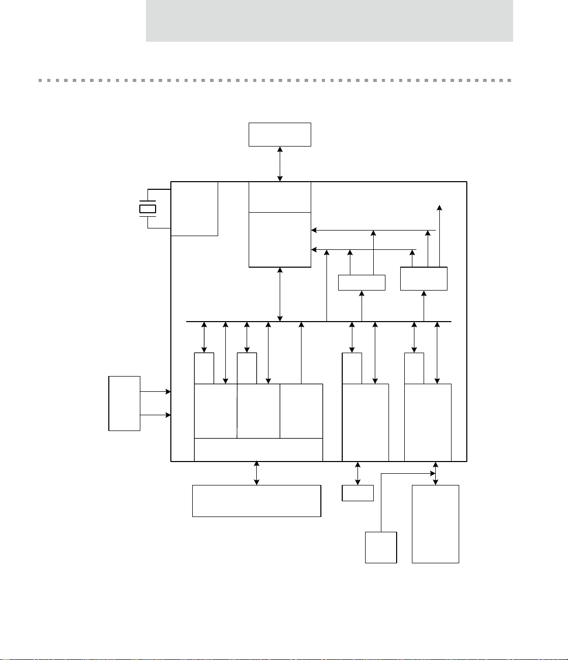
Figure 1 is an overview of the NS7520, including all the modules.
About the NS7520
Debugger
Power
3.3V
1.5V
PLL
System
Clock
BBUS
D
M
A
Serial-A
UART
SPI
JTAG Debug
ARM7TDMI
D
M
A
Serial-B
UART
SPI
16 GPIO
Interface
4
level
interrupt
inputs
FIRQ
IRQ
NS7520
2 timers
D
M
A
Ethernet
controller
802.3
compliant
Reset
Watchdog
timer
D
M
A
External
memory
controller
Address bus
Serial transceivers and other
devices
Figure 1: NS7520 overview
MII
Boot
config
www.digi.com
Memory
devices
Flash
SRAM
FP DRAM
SDRAM
5
Page 20

Operating frequency
Operating frequency
The NS7520 is available in grades operating at three maximum operating frequencies:
36 MHz, 46 MHz, and 55 MHz. The operating frequency is set during bootstrap
initialization, using pins A[8:0]. These address pins load the PLL settings register on
powerup reset. A[8:7] determines IS (charge pump current); A[6:5] determines FS
(output divider), and A[4:0] defines ND (PLL multiplier). Each bit in A[8:0] can be set
individually.
See "Setting the PLL frequency," beginning on page 54, for more detailed
information.
6
NS7520 Hardware Reference, Rev. D 03/2006
Page 21

Pinout and Packaging
CHAPTER 2
The NS7520 can be used in any embedded environment requiring networking
services in an Ethernet LAN. The NS7520 contains an integrated ARM RISC processor,
10/100 Ethernet MAC, serial ports, memory controllers, and parallel I/O. The NS7520
can interface with another processor using a register or shared RAM interface. The
NS7520 provides all the tools required for any embedded networking application.
7
Page 22

Packaging
Packaging
Table 1 provides the NS7520 packaging dimensions. Figure 2 shows the pinout and
NS7520 dimensions. Figure 3 shows the NS7520 BGA layout.
Symbol Min Nom Max
A——1.4
A1 0.35 0.40 0.45
A2——0.95
b 0.45 0.50 0.55
D 13.0 BSC
D1 11.2 BSC
E 13.0 BSC
E1 11.2 BSC
e 0.8 BSC
aaa 0.1
Table 1: NS7520 packaging dimensions
8
NS7520 Hardware Reference, Rev. D 03/2006
Page 23
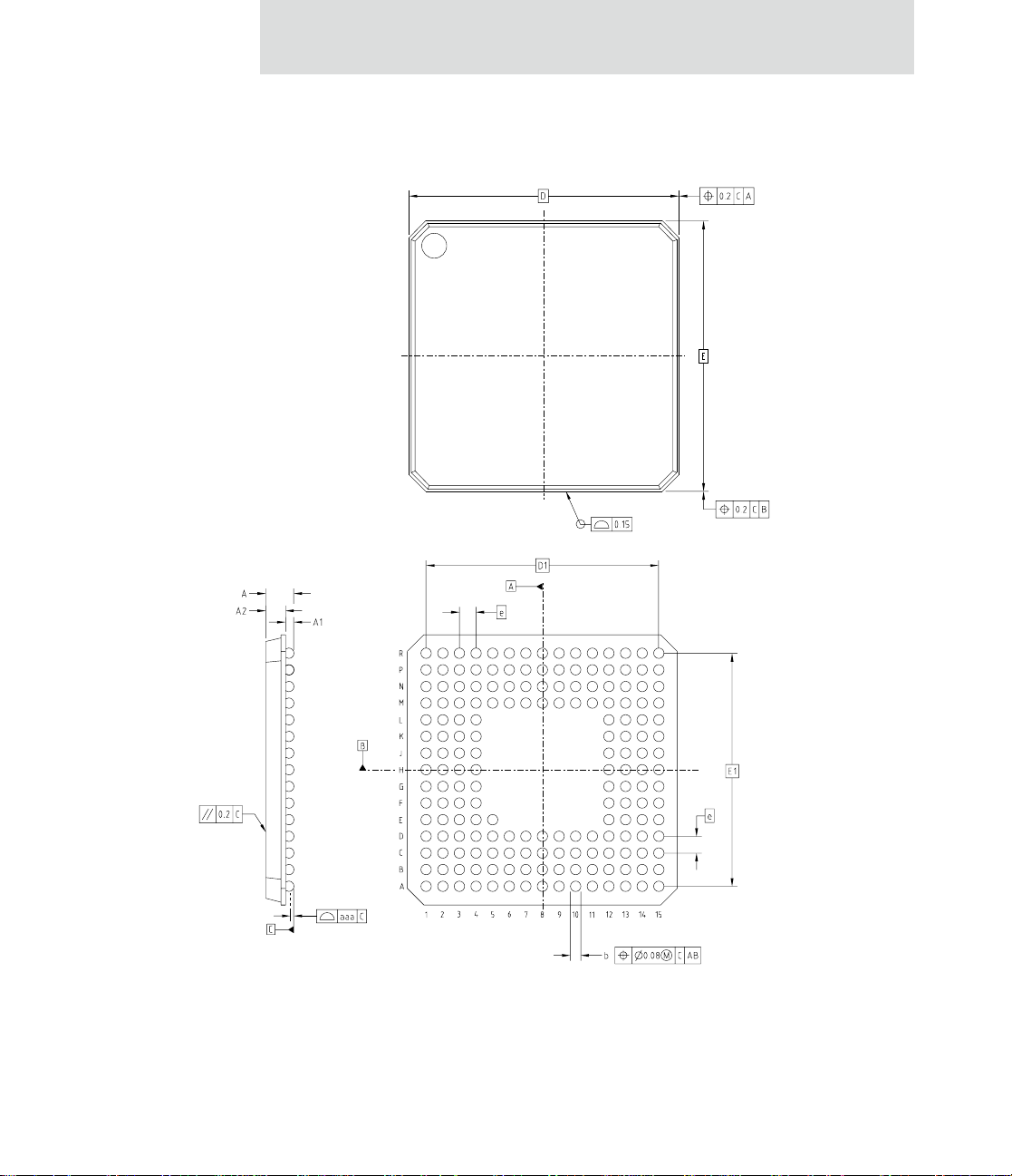
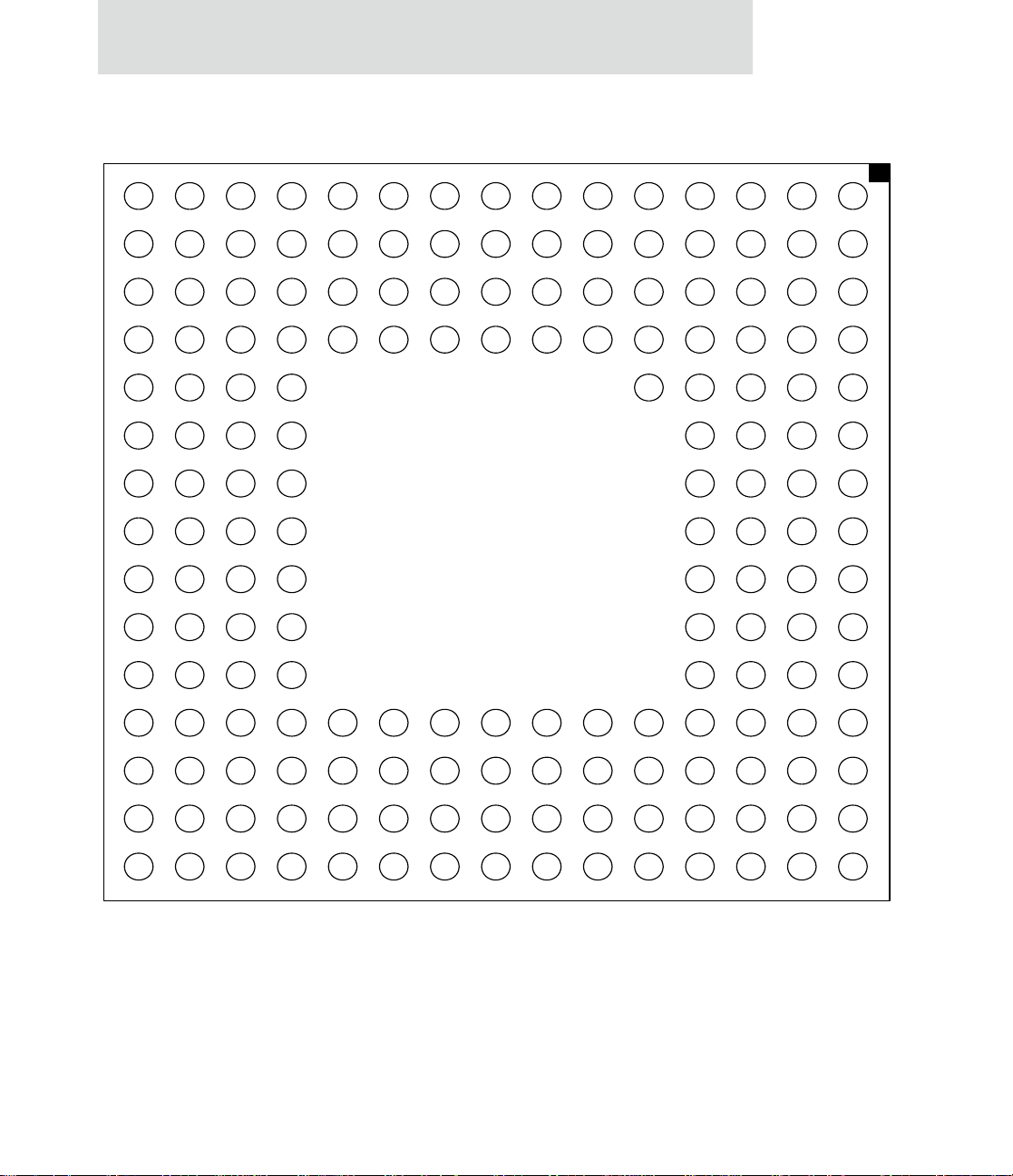
177 PFBGA
Pinout and Packaging
Figure 2: NS7520 pinout and dimensions
www.digi.com
9
Page 24
Packaging
R
P1
R1
A0
A3
R2
P2
A6
GNDPY1
R3
P3 B3
VCCPY2
A7
R4
P4
GNDPY2
A8
P5
R5
VCCPY3
VDDC01
GNDPY11
RESV2+
XTALB2
A10
R6
A13
A15
R7
A17
GNDPY3
R8
A19
R9
VSSC01
A22
R10
P10
A26/0WE_ A27/0OE_
A24
P11
R11
NC2
R12
NC4
RESV1-
P13
R13
NC6
R14
P14
NC5
VSSOSC1
P15
R15
TCK
P6
P7
P8
P9
P
N
N1
D31
N2
A1
N3
VCCPY1
N4
A4
N5
A9
N6
A12
N7
A16
N8
A20
N9
A23
N10
N11
NC3
N12
XTALB1
N13
OSCVCC1
N14
TDI
N15 L15
PLLTST_
M
M1
D30
M2
VCCPY4
M3
A2
M4
A5
M5
A11
M6
A14
M7
A18
M8
GNDPY4
M9
A21
M10
A25
M11
NC1
M12
TMS
M13
TDO
M14
TRST_
M15
BISTEN_
L
L1
L2
D28
L3
D29
L4
D27
L12
PLLVSS
L13
SCANEN_
L14
VDDC02
PLLVDD
E
K
K1
D23
D20
K2 D2
D24
D22
K3
D21
D25
K4
VCCPY5
GNDPY5
H
J
H1
J1
D14
D17
H2 C2
J2
D16
D12
H3
J3
D19
D13
H4
J4
D15
D18
F
G
G1
GNDPY13
G2
D10
G3
G4
D9
D11
F1
F2
F3
F4
E1
D8
E2
D7
E3
D6
E4
VCCPY8
E5
GUIDE PIN
NS7520, 177 PFBGA
Top View, Balls Facing Down
V1.0
K12
XTAL2
K13
VSSC02
K14
XTAL1
K15
GNDPY12
J12
PORTA4
J13
PORTA6
PORTA7
J15
PORTA5
H12
H13
PORTA1
H14
VCCPY6
H15
PORTA3
G12
PORTA0
G13
PORTC7
G14
PORTC6
G15
GNDPY6
PORTC4
PORTC3
VCCPY7
PORTC5
F12
F13
F14
F15
E12
PORTC1
E13
GNDPY7
E14
PORTC0
E15
PORTC2
C
D
D1
D5
GNDPY8
D3 A3
OSCVCC2
D1
D4
D2
CAS2_
D5
CS2_
CS0_
D6
RW_
WE_
D7
BR_
BG_
D8
TEA_
TA_
D9
BE1_
BE3_
D10
C10
MDC
TXCLK
D11
C11
GNDPY14
TXD1
C12
D12
RXCRS
RXCLKPORTA2
D13
C13
VDDC04
VSSC04
C14
D14
VDDC03
RXD3
C15
D15
RXDV
RXER
B
B1
C1
D3D26
D4
B2
D0
VSSOSC2
C3
CAS1_
C4
B4
CS4_
C5
B5
CS1_
C6
B6
OE_
C7
B7
BUSY_
B8
C8
VCCPY10
B9
C9
BE0_
B10
MDIO
B11
TXD2
B12
TXEN
B13
RXD0
B14
VSSC03
B15
RXD2
A
A1
CAS3_
A2
CAS0_
VCCPY9
A4
CS3_
A5
GNDPY9
A6
BCLK
A7
GNDPY10
A8
TS_
A9
BE2_
A10
RESET_
A11
TXD0
A12P12
TXD3
A13
TXER
A14J14
TXCOL
A15
RXD1
1
2
3
4
5
6
7
8
9
10
11
12
13
14
15
Figure 3: NS7520 BGA layout
10
NS7520 Hardware Reference, Rev. D 03/2006
Page 25

Pinout detail tables and signal descriptions
Each pinout table applies to a specific interface and contains the following
information:
Column Description
Signal The pin name for each I/O signal. Some signals have multiple function modes and
are identified accordingly. The mode is configured through firmware using one or
more configuration registers.
Pin The pin number assignment for a specific I/O signal.
U next to the pin number indicates that the pin is a pullup resistor (input
current source).
D next to the pin number indicates that the pin is a pulldown resistor (input
current sink).
No value next to the pin indicates that the pin has neither a pullup nor
pulldown resistor.
See Figure 28, "Internal pullup characteristics," on page 264 and Figure 29,
"Internal pulldown characteristics," on page 264 for an illustration of the
characteristics of these pins. Use the figures to select the appropriate value of the
complimentary resistor to drive the signal to the opposite logic state. For those
pins with no pullup or pulldown resistor, you must select the appropriate value per
your design requirements.
Pinout and Packaging
_ An underscore (bar) indicates that the pin is active low.
I/O The type of signal — input, output, or input/output.
OD The output drive strength of an output buffer. The NS7520 uses one of three
drivers:
2 mA
4 mA
8 mA
Notes:
NO CONNECT as a description for a pin means do not connect to this pin.
The 177th pin (package ball) is for alignment of the package on the PCB.
www.digi.com
11
Page 26

Pinout detail tables and signal descriptions
System bus interface
Symbol Pin I/O OD Description
BCLK A6 O 8 Synchronous bus clock
External bus Other External bus Other
ADDR27 CS0OE_ N10 U I/O 4 Addr bit 27 Logical AND of CS0_
ADDR26 CS0WE_ P10 U I/O 4 Addr bit 26 Logical AND of CS0_
External bus External bus
ADDR25 M10 U I/O 4 Remainder of address bus (through
ADDR24 R10 U I/O 4
ADDR23 N9 U I/O 4
ADDR22 R9 U I/O 4
ADDR21 M9 U I/O 4
and OE_
and WE_
ADDR0)
ADDR20 N8 U I/O 4
ADDR19 P8 U I/O 4
ADDR18 M7 U I/O 4
ADDR17 R7U I/O 4
ADDR16 N7 U I/O 4
ADDR15 R6 U I/O 4
ADDR14 M6 U I/O 4
ADDR13 P6 U I/O 4
ADDR12 N6 U I/O 4
ADDR11 M5 U I/O 4
ADDR10 P5 U I/O 4
ADDR9 N5 U I/O 4
ADDR8 R4 U I/O 4
Table 2: System bus interface pinout
12
NS7520 Hardware Reference, Rev. D 03/2006
Page 27

Symbol Pin I/O OD Description
ADDR7 R3 U I/O 4
ADDR6 R2 U I/O 4
ADDR5 M4 U I/O 4
ADDR4 N4 U I/O 4
ADDR3 R1 U I/O 4
ADDR2 M3 U I/O 4
ADDR1 N2 U I/O 4
ADDR0 P1 U I/O 4
DATA31 N1 I/O 4 Data bus
DATA30 M1 I/O 4
DATA29 L3 I/O 4
DATA28 L2 I/O 4
DATA27 L4 I/O 4
DATA26 L1 I/O 4
Pinout and Packaging
DATA25 K3 I/O 4
DATA24 K2 I/O 4
DATA23 K1 I/O 4
DATA22 J2 I/O 4
DATA21 J3 I/O 4
DATA20 J1 I/O 4
DATA19 H3 I/O 4
DATA18 H4 I/O 4
DATA17 H1 I/O 4
DATA16 H2 I/O 4
DATA15 G4 I/O 4
DATA14 G1 I/O 4
DATA13 G3 I/O 4
Table 2: System bus interface pinout
www.digi.com
13
Page 28

Pinout detail tables and signal descriptions
Symbol Pin I/O OD Description
DATA12 G2 I/O 4
DATA11 F4 I/O 4
DATA10 F2 I/O 4
DATA9 F3 I/O 4
DATA8 E1 I/O 4
DATA7 E2 I/O 4
DATA6 E3 I/O 4
DATA5 D1 I/O 4
DATA4 C1 I/O 4
DATA3 B1 I/O 4
DATA2 D4 I/O 4
DATA1 D3 I/O 4
DATA0 C2 I/O 4
BE3_ D9 I/O 2 Byte enable D31:D24
BE2_ A9 I/O 2 Byte enable D23:D16
BE1_ C9 I/O 2 Byte enable D15:D08
BE0_ B9 I/O 2 Byte enable D07:D00
TS_ A8 U I/O 4 DO NOT USE
TA_ D8 U I/O 4 Data transfer acknowledge
Table 2: System bus interface pinout
14
Add an external 820 ohm pullup to 3.3 V.
Add an external 820 ohm pullup to 3.3 V.
TA_ is bidirectional. It is used in input
mode to terminate a memory cycle
externally. It is used in output mode for
reference purposes only.
NS7520 Hardware Reference, Rev. D 03/2006
Page 29

Pinout and Packaging
Symbol Pin I/O OD Description
TEA_ C8 U I/O 4 Data transfer error acknowledge
Add an external 820 ohm pullup to 3.3 V.
TEA_ is bidirectional. It is used in input
mode to terminate a memory cycle
externally. It is used in output mode for
reference purposes only.
RW_ D6 I/O 2 Transfer direction
BR_ D7 NO CONNECT
BG_ C7 NO CONNECT
BUSY_ B7 NO CONNECT
Table 2: System bus interface pinout
Signal descriptions
Mnemonic Signal Description
BCLK Bus clock Provides the bus clock. All system bus interface
signals are referenced to the BCLK signal.
ADDR[27:0] Address bus Identifies the address of the peripheral being
addressed by the current bus master. The address
bus is bi-directional.
DATA[31:0] Data bus Provides the data transfer path between the
NS7520 and external peripheral devices. The data
bus is bi-directional.
Recommendation: Less than x32 (S)DRAM/SRAM
memory configurations. Unconnected data bus
pins will float during memory read cycles. Floating
inputs can be a source of wasted power.
For other than x32 DRAM/SRAM configurations,
the unused data bus signals should be pulled up.
TS_ Transfer start NO CONNECT
BE_ Byte enable Identifies which 8-bit bytes of the 32-bit data bus
are active during any given system bus memory
cycle. The BE_ signals are active low and
bi-directional.
Table 3: System bus interface signal description
www.digi.com
15
Page 30

Pinout detail tables and signal descriptions
Mnemonic Signal Description
TA_ Transfer acknowledge Indicates the end of the current system bus
memory cycle. This signal is driven to 1 prior to
tri-stating its driver.
TA_ is bi-directional.
TEA_ Transfer error
RW_ Read/write indicator Indicates the direction of the system bus memory
BR_ Bus request NO CONNECT
BG_ Bus grant NO CONNECT
BUSY_ Bus busy NO CONNECT
Table 3: System bus interface signal description
Chip select controller
acknowledge
Indicates an error termination or burst cycle
termination:
In conjunction with TA_ to signal the end of a
burst cycle.
Independently of TA_ to signal that an error
occurred during the current bus cycle. TEA_
terminates the current burst cycle.
This signal is driven to 1 prior to tri-stating its
driver.
TEA_ is bi-directional. The NS7520 or the external
peripheral can drive this signal.
cycle. RW_ high indicates a read operation; RW_
low indicates a write operation. The RW_ signal is
bi-directional.
The NS7520 supports five unique chip select configurations:
Symbol Pin I/O OD Description
CS4_ B4 O 4 Chip select/DRAM RAS_
CS3_ A4 O 4 Chip select/DRAM RAS_
CS2_ C5 O 4 Chip select/DRAM RAS_
CS1_ B5 O 4 Chip select/DRAM RAS_
Table 4: Chip select controller pinout
16
NS7520 Hardware Reference, Rev. D 03/2006
Page 31

Pinout and Packaging
Symbol Pin I/O OD Description
CS0_ D5 O 4 Chip select (boot select)
CAS3_ A1 O 4 FP/EDO DRAM column strobe
D31:D24/SDRAM RAS_
CAS2_ C4 O 4 FP/EDO DRAM column strobe
D23:D16/SDRAM CAS_
CAS1_ B3 O 4 FP/EDO DRAM column strobe
D15:D08/SDRAM WE_
CAS0_ A2 O 4 FP/EDO DRAM column strobe
D07:D00/SDRAM A10(AP)
WE_ C6 O 4 Write enable for NCC Ctrl’d cycles
OE_ B6 O 4 Output enable for NCC Ctrl’d cycles
Table 4: Chip select controller pinout
Signal descriptions
Mnemonic Signal Description
CS0_
CS1_
CS2_
CS3_
CS4_
Chip select 0
Chip select 1
Chip select 2
Chip select 3
Chip select 4
Unique chip select outputs supported by the
NS7520. Each chip select can be configured to
decode a portion of the available address space
and can address a maximum of 256 Mbytes of
address space. The chip selects are configured
using registers in the memory module.
A chip select signal is driven low to indicate the
end of the current memory cycle. For FP/EDO
DRAM, these signals provide the RAS signal.
Table 5: Chip select controller signal description
www.digi.com
17
Page 32

Pinout detail tables and signal descriptions
Mnemonic Signal Description
CAS0_
CAS1_
CAS2_
CAS3_
WE_ Write enable Active low signal that indicates that a memory
OE_ Output enable Active low signal that indicates that a memory read
Table 5: Chip select controller signal description
Ethernet interface MAC
Column address strobe
signals
Activated when an address is decoded by a chip
select module configured for DRAM mode. The
CAS_ signals are active low and provide the
column address strobe function for DRAM devices.
The CAS_ signals also identify which 8-bit bytes of
the 32-bit data bus are active during any given
system bus memory cycle.
For SDRAM, CAS[3:1]_ provides the SDRAM
command field. CAS0_ provides the
auto-precharge signal.
For non-DRAM settings, these signals are 1.
write cycle is in progress. This signal is activated
only during write cycles to peripherals controlled
by one of the chip selects in the memory module.
cycle is in progress. This signal is activated only
during read cycles from peripherals controlled by
one of the chip selects in the memory module.
Note:
In this table, GP designates general-purpose.
Symbol Pin I/O OD Description
MII ENDEC MII ENDEC
MDC GP output D10 O 2 MII
MDIO GP output B10 U I/O 2 MII data State of UTP_STP bit
TXCLK C10 I TX clock
Table 6: Ethernet interface MAC pinout
18
ENDEC values for general-purpose output and TXD refer to bits in the
Ethernet General Control register. ENDEC values for general-purpose input
and RXD refer to bits in the Ethernet General Status register.
State of (LPBK bit XOR
management
clock
NS7520 Hardware Reference, Rev. D 03/2006
(Mode=SEEQ))
Page 33

Pinout and Packaging
Symbol Pin I/O OD Description
TXD3 GP output A12 O 2 TX data 3 State of AUI_TP[0] bit
TXD2 GP output B11 O 2 TX data 2 State of AUI_TP[1] bit
TXD1 GP output D11 O 2 TX data 1 Inverted state of PDN
bit, open collector
TXD0 TXD A11 O 2 TX data 0 Transmit data
TXER GP output A13 O 2 TX code error State of LNK_DIS_ bit
TXEN B12 O 2 TX enable
TXCOL A14 I Collision
RXCRS D12 I Carrier sense
RXCLK C12 I RX clock
RXD3 GP input D14 I RX data 3 Read state in bit 12
RXD2 GP input B15 I RX data 2 Read state in bit 15
RXD1 GP input A15 I RX data 1 Read state in bit 13
RXD0 RXD B13 I RX data 0 Receive data
RXER GP input C15 I RX error Read state in bit 11
RXDV GP input D15 I RX data valid Read state in bit 10
Table 6: Ethernet interface MAC pinout
Signal descriptions
The Ethernet MII (media independent interface) provides the connection between the
Ethernet PHY and the MAC (media access controller).
Mnemonic Signal Description
MDC MII management clock Provides the clock for the MDIO serial data
channel. The MDC signal is an NS7520 output.
The frequency is derived from the system
operating frequency per the CLKS field setting (see
the CLKS field in Table 69: "MII Management
Configuration register bit definition" on page 191).
Table 7: Ethernet interface MAC signal description
www.digi.com
19
Page 34

Pinout detail tables and signal descriptions
Mnemonic Signal Description
MDIO Management data IO A bi-directional signal that provides a serial data
TXCLK T ransmit clock An input to the NS7520 from the external PHY
channel between the NS7520 and the external
Ethernet PHY module.
module. TXCLK provides the synchronous data
clock for transmit data.
TXD3
TXD2
TXD1
TXD0
Transmit data signals Nibble bus used by the NS7520 to drive data to the
external Ethernet PHY. All transmit data signals are
synchronized to TXCLK.
In ENDEC mode, only TXD0 is used for transmit
data.
TXER Transmit coding error Output asserted by the NS7520 when an error has
occurred in the transmit data stream.
TXEN Transmit enable Asserted when the NS7520 drives valid data on
the TXD outputs. This signal is synchronized to
TXCLK.
COL Transmit collision Input signal asserted by the external Ethernet PHY
when a collision is detected.
CRS Receive carrier sense Asserted by the external Ethernet PHY whenever
the receive medium is non-idle.
RXCLK Receive clock An input to the NS7520 from the external PHY
module. The receive clock provides the
synchronous data clock for receive data.
RXD3
RXD2
RXD1
RXD0
Receive data signals Nibble bus used by the NS7520 to input receive
data from the external Ethernet PHY. All receive
data signals are synchronized to RXCLK.
In ENDEC mode, only RXD0 is used for receive
data.
RXER Receive error Input asserted by the external Ethernet PHY when
RXDV Receive data valid Input asserted by the external Ethernet PHY when
Table 7: Ethernet interface MAC signal description
20
the Ethernet PHY encounters invalid symbols from
the network.
the PHY drives valid data on the RXD inputs.
NS7520 Hardware Reference, Rev. D 03/2006
Page 35

“No connect” pins
Pin Description
Pinout and Packaging
R13 Tie to V
P12 Tie to V
N12 XTALB1: Tie to V
R15 XTALB2: NO CONNECT
M11 NO CONNECT
P11 NO CONNECT
N11 NO CONNECT
R12 NO CONNECT
R14 NO CONNECT
P13 NO CONNECT
Table 8: “No connect” pins
General-purpose I/O
GPIO
signal
PORTA7 TXDA J14 U I/O 2 Channel 1 TXD
Serial
signal
CC
CC
Other
signal
CC
Pin I/O OD
Serial channel
description
Other
description
PORTA6 DTRA_ DREQ1_ J13 U I/O 2 Channel 1
DTR_
PORTA5 RTSA_ J15 U I/O 2 Channel 1
RTS_
PORTA4 RXCA/
RIA_/
OUT1A_
J12 U I/O 2 Pgm’able Out/
Channel 1
RXCLK/
Channel 1 ring
signal/Channel
1 SPI clock
(CLK)
Table 9: GPIO pinout
www.digi.com
DMA channel
3/5 Req
21
Page 36

Pinout detail tables and signal descriptions
GPIO
signal
Serial
signal
Other
signal
Pin I/O OD
Serial channel
description
Other
description
PORTA3 RXDA DACK1_ H15 U I/O 2 Channel 1 RXD DMA channel
3/5 ACK
PORTA2 DSRA_ AMUX H12 U I/O 2 Channel 1
DSR_
PORTA1 CTSA_ DONE1_
(O)
PORTA0 TXCA/
DONE1_ (I) G12 U I/O 2 Pgm’able Out/
OUT2A_/
DCDA_
H13 U I/O 2 Channel 1
CTS_
Channel 1
DCD/Channel 1
DRAM addr
mux
DMA channel
3/5 DONE_Out
DMA channel
3/5 DONE_In
SPI enable
(SEL_)/Channel
1 TXCLK
PORTC7 TXDB G13 U I/O 2 Channel 2 TXD GEN interrupt
out
PORTC6 DTRB_ DREQ2_ G14 U I/O 2 Channel 2
DTR_
PORTC5 RTSB_ REJECT_ F15 U I/O 2 Channel 2
DMA channel
4/6 Req
CAM reject
RTS_
PORTC4 RXCB/RIB_/
OUT1B_
RESET_ F12 U I/O 2 Pgm’able Out/
Channel 2
RXCLK/
Channel 2 ring
RESET output
See Note 1
following this
table.
signal/Channel
2 SPI clock
(CLK)
PORTC3
RXDB LIRQ3/
DACK2_
F13 U I/O 2 Channel 2 RXD Level sensitive
IRQ/DMA
2
channel 4/6
ACK
PORTC2
DSRB_ LIRQ2/
RSPF_
E15 U I/O 2 Channel 2
DSR_
Level sensitive
IRQ/CAM
2
request
PORTC1
CTSB_ LIRQ1/
DONE2_
(O)
E12 U I/O 2 Channel 2
CTS_
Level sensitive
IRQ/DMA
channel 4/6
2
DONE_out
Table 9: GPIO pinout
22
NS7520 Hardware Reference, Rev. D 03/2006
Page 37

Pinout and Packaging
GPIO
signal
PORTC02TXCB/
Serial
signal
OUT2B_/
DCDB_
Other
signal
LIRQ0/
DONE2_(I)
Serial channel
Pin I/O OD
E14 U I/O 2 Pgm’able Out/
description
Channel 2
DCD/Channel 2
SPI enable
(SEL_)/Channel
2 TXCLK
Other
description
Level sensitive
IRQ/DMA
channel 4/6
DONE_in
Table 9: GPIO pinout
Notes:
1 RESET output indicates the reset state of the NS7520. PORTC4 persists beyond
the negation of RESET_ for approximately 512 clock cycles if the PLL is dis abled.
When the PLL is enabled, PORTC4 persists beyond the negation of RESET_ to
allow for PLL lock for 100 microseconds times the ratio of the VCO to XTALA.
Note that this GPIO is left in output mode active following a hardware
RESET.
2 *PORTC[3:0] pins provide level-sensitive interrupts. The inputs do not need to
be synchronous to any clock. The interrupt remains active until cleared by a
change in the input signal level.
Signal descriptions
See Chapter 6, "GEN Module," for signal and configuration information for PORTA and
PORTC.
www.digi.com
23
Page 38

Pinout detail tables and signal descriptions
System clock and reset
Symbol Pin I/O OD Description
XTALA1 K14 I ARM/system oscillator circuit
XTALA2 K12 O
PLLVDD (1.5V) L15 P PLL clean power
PLLVSS L12 P PLL return
RESET_ A10 I System reset
Table 10: System clock pinout
Signal descriptions
The NS7520 has three clock domains:
System clock (SYSCLK)
Bit rate generation and programmable timer reference clock (XTALA1/2)
System bus clock (BCLK)
The SYS module provides the NS7520 with these clocks, as well as system reset and
backup resources.
Mnemonic Signal Description
XTALA1
XTALA2
PLLVDD
PLLVSS
RESET_ System reset Resets the NS7520 hardware.
Table 11: Clock generation and reset signal d escription
24
Oscillator input
Oscillator output
Clean PLL power
Connect directly to the
GND plane
NS7520 Hardware Reference, Rev. D 03/2006
A standard parallel quartz crystal or crystal
oscillator can be attached to these pins to provide
the main input clock to the NS7520.
Power and ground for PLL circuit.
Page 39

Pinout and Packaging
This figure shows the timing and specification for RESET_ rise/fall times:
tF tR
tF max = 18ns
V in = 2.0V to 0.8V
System mode (test support)
PLLTST_, BISTEN_, and SCANEN_ primary inputs control differen t test modes for both
functional and manufacturing test operations. See Chapter 5, "SYS Module," for more
information.
Symbol Pin I/O OD Description
PLLTST_ N15 I Encoded with BISTEN_ and SCANEN_
BISTEN_ M15 I Encoded with PLLTST_ and SCANEN_
SCANEN_ L13 I Encoded with BISTEN_ and PLLTST_
Table 12: System mode and system reset pinout
tR max = 18ns
V in = 0.8V to 2.0V
Add an external pullup to 3.3V or
pulldown to GND.
Add an external pullup to 3.3V or
pulldown to GND.
Add an external pullup to 3.3V or
pulldown to GND.
www.digi.com
25
Page 40

Pinout detail tables and signal descriptions
JTAG test (ARM debugger)
JTAG boundary scan allows a tester to check the soldering of all signal pins and tristate all outputs.
Symbol Pin I/O OD Description
TDI N14 U I Test data in
TDO M13 O 2 Test data out
TMS M12 U I Test mode select
TRST_ M14 I Test mode reset
TCK P15 I Test mode clock
Table 13: JTAG test pinout
Requires external termination when not
being used (see Figure 4, "TRST_
termination," on page 27 for an
illustration of the termination circuit on
the development PCB).
Add an external pullup to 3.3V.
Signal descriptions
Mnemonic Signal Description
TDI Test data in TDI operates the JTAG standard. Consult the
TDO Test data out TDO operates the JTAG standard. Consult the
TMS Test mode select TMS operates the JTAG standard. Consult the
Table 14: ARM debugger signal description
26
JTAG specifications for use in boundary-scan
testing. These signals meet the requirements of the
Raven and Jeeni debuggers.
JTAG specifications for use in boundary-scan
testing. These signals meet the requirements of the
Raven and Jeeni debuggers.
JTAG specifications for use in boundary-scan
testing. These signals meet the requirements of the
Raven and Jeeni debuggers.
NS7520 Hardware Reference, Rev. D 03/2006
Page 41

Pinout and Packaging
Mnemonic Signal Description
TRST_ Test mode reset TRST_ operates the JTAG standard. Consult the
JTAG specifications for use in boundary-scan
testing. These signals meet the requirements of the
Raven and Jeeni debuggers.
TCK Test mode clock TCK operates the JTAG standard. Consult the
JTAG specifications for use in boundary-scan
testing. These signals meet the requirements of the
Raven and Jeeni debuggers.
Table 14: ARM debugger signal description
NS7520
Figure 4: TRST_ termination
www.digi.com
TRSTNS7520
27
Page 42

Pinout detail tables and signal descriptions
Power supply
Signal Pin Description
Oscillator VCC (3.3V) N13, C3 Oscillator power supply
Core VCC (1.5V) R8, L14, C14, C13 Core power supply
I/O VCC (3.3V) E4, K4, M2, N3, P3, R5, H14, F14, B8, A3I/O power supply
GND D2, F1, J4, P4, P7, M8, P9, R11, K15,
G15, E13, D13, B14, C11, A7, A5, B2,
P2, P14, K13
Ground
Table 15: Power supply pinout
See the DC and AC electrical specifications in Chapter 11, "Electrical Characteristics,"
for more information.
28
NS7520 Hardware Reference, Rev. D 03/2006
Page 43

Working with the CPU
CHAPTER 3
The CPU uses an ARM7TDMI core processor, which provides high performance while
maintaining low power consumption and small size. This chapter describes the ARM
Thumb concept and provides an overview of ARM exceptions and hardware interrupts.
29
Page 44

ARM Thumb concept
ARM Thumb concept
The ARM7TDMI processor uses a unique architectural strategy known as Thumb, which
makes the processor ideally suited to high-volume applications with memory
restrictions or applications for which code density is an issue.
Thumb code’s primary attribute is a super-reduced instruction set. The ARM7TDMI
processor has essentially two instruction sets:
Standard 32-bit ARM set
16-bit Thumb set
Thumb’s 16-bit instruction length allows it to approach twice the density of standard
ARM code while retaining most of the ARM’s performance advantage over a
traditional 16-bit processor using 16-bit registers. Thumb code operates on the same
32-bit register set as the ARM code, but consumes only 65% of the same code
compiled in ARM mode.
Thumb instructions operate with the standard ARM register configuration, allowing
interoperability between ARM and Thumb states. Each 16-bit Thumb instruction has a
corresponding 32-bit ARM instruction with the same effect on the processor model.
Thumb architecture provides a Thumb instruction decoder in front of the standard
32-bit ARM processor. The Thumb instruction decoder basically remaps each 16-bit
Thumb instruction into a 32-bit standard ARM instruction. The Thumb instruction set
typically requires 30% more instructions to perform the same task as 32-bit
instructions, but the Thumb instruction can fit twice as many instructions in the code
space. The net result is a 35% decrease in overall code density.
CPU performance
The ARM7TDMI core does not contain cache, and runs as fast as instructions can be
fetched. The performance rating for the ARM RISC depends on system bus speed and
cycle time. Performance is also affected by the size of the system bus and the type of
code (ARM or Thumb) being executed.
30
NS7520 Hardware Reference, Rev. D 03/2006
Page 45

Working with the CPU
The ARM instruction set yields a 0.9 Dhrystone (2.1) rating MIPS/MHz of instruction
executions; the Thumb instruction set yields 0.75 Dhrystones MIPS/MHz. The MHz
rating reflects the rate at which instructions can be fetched from external flash
memory, as shown in this table:
System bus
size Code style RISC speed
Thumb mode
16-bit Thumb 25 MHz 25 MHz 1 120 ns N/A
16-bit Thumb 25 MHz 25 MHz 0 80 ns N/A
16-bit Thumb 36 MHz 36 MHz 3 125 ns N/A
16-bit Thumb 46 MHz 46 MHz 4 109 ns N/A
16-bit Thumb 55 MHz 55 MHz 5 108 ns N/A
ARM mode
32-bit ARM 36 MHz 36 MHz 3 125 ns 6.8
32-bit ARM 46 MHz 46 MHz 4 109 ns 8.6
32-bit ARM 55 MHz 55 MHz 5 108 ns 10.4
System bus
speed
Wait
states
Instruction
cycle time
Dhrystone
rating
Table 16: ARM performance
Working with ARM exceptions
Exceptions occur when the normal flow of a program is halted temporarily; for
example, to service an interrupt from a peripheral. Each ARM exception causes the
ARM processor to save some state information, then jump to a location in low
memory (referred to as the vector table; see "Exception vector table" on page 33).
Before an exception can be handled, the current processor state must be preserved
so the original program can resume when the handler routine has finished.
www.digi.com
31
Page 46

Working with ARM exceptions
Summary of ARM exceptions
The ARM processor can be interrupted by any of seven basic exceptions:
Reset exception. After a reset condition, the ARM7TDMI saves the current
values of the PC (program counter) and CPSR (Current Processor Status
register).
Undefined exception. The ARM7TDMI takes the undefined instruction trap
when it finds an instruction it cannot handle.
SWI instruction. The ARM7TDMI uses the software interrupt instruction
(SWI) to enter supervisor mode, usually to request a specific supervisor
instruction.
Abort exception. An abort exception indicates that the current memory
access cannot be completed. There are two types of abort exception:
– Prefetch. Occurs during an instruction prefetch.
– Data. Occurs during a data operand access.
IRQ. An interrupt request (IRQ) exception is a normal interrupt serviced by
the ARM7TDMI controller.
FIRQ. A fast interrupt request (FIRQ) exception supports a data transfer or
channel process. An FIRQ interrupt is generated only by the GEN module
timers and watchdog timer.
Exception priorities
Several exceptions can occur at the same time. If this happens, a fixed-priority
system determines the order in which they are handled:
Highest priority
1 Reset
2 Data abort
3 FIRQ
4 IRQ
5 Prefetch abort
6 Undefined instruction, SWI
Lowest priority
32
NS7520 Hardware Reference, Rev. D 03/2006
Page 47

Not all exceptions can occur at the same time, however.
Undefined instructions and SWIs are mutually exclusive, as they each
correspond to particular (non-overlapping) decoding of the current
instruction.
If a data abort occurs at the same time as FIRQ and the FIRQ is enabled
(that is, the CPSR F flag is clear), the data abort takes priority. ARM7TDMI
enters the data abort handler and immediately goes to the FIRQ vector. A
normal return from FIRQ causes the data abort handler to resume
execution.
Placing data abort at a higher priority than FIRQ is necessary to ensure
that the transfer error does not escape detection. The time for this
exception entry should be added to worst-case FIRQ latency
calculations.
Exception vector table
All exceptions result in the ARM processor vectoring to an address in low memory,
using the exception vector table. The exception vector table always exists and always
starts at base address 0.
Working with the CPU
Vector
address
’h0 RESET Reset vector; for initialization and startup
’h4 Undefined Undefined instruction encountered
’h8 SWI Software interrupt; used for entry point into the kerne l
’hC Abort (prefetch) Bus error (no response or error) fetching instructions
’h10 Abort (data) Bus error (no response or error) fetching data
’h14 Reserved Reserved
’h18 IRQ Interrupt from ARM7TDMI interrupt controller
’h1C FIRQ Fast interrupt from ARM7TDMI controller
Vector Description
Table 17: Exception vector table
www.digi.com
33
Page 48

Working with ARM exceptions
All internal ARM7TDMI internal peripherals are presented to the CPU using the IRQ or
FIRQ interrupt inputs. The ARM can mask various ARM7TDMI peripheral interrupts at
the global level, using the ARM7TDMI interrupt controller. The ARM also can mask
interrupts at the micro-level, using configuration features with the peripheral
modules.
All IRQ interrupts are disabled when the I bit is set in the ARM CPSR. When the I bit is
cleared, those interrupts enabled in the ARM7TDMI interrupt controller can assert the
IRQ input to the ARM processor.
The ARM processor sets the I bit automatically when entering an interrupt service
routine (ISR), which disables recursive interrupts. The ISR’s first task is to read the
Interrupt Status register, which identifies all active sources for the IRQ interrupt.
Firmware sets the priorities for servicing interrupts at bootup, using the bits defined
in the Interrupt Status register.
Detail of ARM exceptions
Reset exception
A reset exception is the highest priority exception. When the ARM7TDMI is held in
reset, the processor abandons the executing instruction and cont inu es to fetch
instructions from incrementing word addresses.
When the ARM7TDMI is removed from reset, the processor performs these steps:
1 Overwrites R14_svc and SPSR_svc (Saved Processor Status register) by copying the
2 Forces the CPSR M field to 10011 (supervisor mode), sets the I and F bits in the
3 Forces the PC to fetch the next instruction from address ’h00.
4 Resumes execution in ARM state.
Undefined exception
When the ARM7TDMI encounters an instruction it cannot handle, it takes the
undefined instruction trap. The undefined instruction trap can extend either the
Thumb or ARM instruction set by software emulation.
34
current values of the PC and CPSR into them. The values of the saved PC and
SPSR are not defined.
CPSR, and clears the CPSR T bit (back to ARM mode).
NS7520 Hardware Reference, Rev. D 03/2006
Page 49

Working with the CPU
After emulating the failed instruction, t h e trap handler should execute the following
instruction irrespective of the state (Thumb or ARM):
MOVS PC, R14_und.
This instruction restores the PC and CPSR, and returns to the instruction following the
undefined instruction.
SWI exception
An SWI is used for entering supervisor mode, usually to request a particular supervisor
function. An SWI handler should return by executing this instruction irrespective of
the state (ARM or Thumb):
MOVS PC, R14_SVC.
This instruction restores the PC and CPSR, and returns to the instruction following the
SWI.
Abort exception
An abort indicates that the current memory access cannot be completed, and is
signaled by the external ABORT input. The ARM7TDMI checks for the abort exception
during memory access cycles.
There are two types of abort exception:
Prefetch abort. Occurs during an instruction prefetch. If a prefetch abort
occurs, the prefetch instruction is marked as invalid but the exception is
not taken until the instruction reaches the head of the pipeline. If the
instruction is not executed (for example, if a branch occurs while the
instruction is in the pipeline), the abort does not take place.
Data abort. Occurs during a data operand access. If a data abort occurs, the
action taken depends on the instruction type:
– Single data transfer instructions (LDR, STR) write back modified base
registers; the abort handler must be aware of this.
– A swap instruction (SWP) is aborted as though it had not been executed.
– Block data transfer instructions (LDM, STM) complete. If write-back is set,
the base is updated. If the instruction would have overwritten the base with
data (that is, the base is in the transfer list), the overwriting is prevented.
All register overwriting is prevented after an abort is indicated, which
means that
R15 (always the last register to be transferred) is preserved in an
aborted LDM instruction.
www.digi.com
35
Page 50

Working with ARM exceptions
The abort mechanism allows the implementation of a demand-paged virtual memory
system. In this type of system, the processor is allowed to generate arbitrary
addresses. When the data at an address is unavailable, the memory management unit
(MMU) signals an abort. The abort handler must then work out the cause of the abort,
make the requested data available, and retry the aborted instruction. The
application program needs no knowledge of the amount of memory available to it,
and its state is not affected by the abort.
The handler executes one of the following instructions, irrespective of the state (ARM
or Thumb), after fixing the cause of the abort:
For a prefetch abort: SUBS PC, R14_abt, #4
For a data abort: SUBS PC, R14_abt, #8
IRQ exception
An IRQ exception is a normal interrupt sourced by the ARM7TDMI interrupt controller.
IRQ has a lower priority than FIRQ, and is masked out when an FIRQ sequence is
entered. IRQ can be disabled at any time by setting the I bit in CPSR to 1; this can be
done only from privileged (non-user) mode.
The IRQ handler should leave the interrupt by executing the following instruction
irrespective of the state (ARM or Thumb):
FIRQ exception
An FIRQ exception supports a data transfer or channel process. In ARM state, FIRQ has
enough registers to remove the need for register saving, which minimizes context
switching overhead.
Only two peripherals can generate an FIRQ interrupt: the GEN module built-in timers
and the GEN module watchdog timer.
The FIRQ handler should leave the interrupt by executing the following instruction
irrespective of the state (ARM or THUMB):
The FIRQ interrupt can be disabled by setting the CPSR F flag to 1, only in non-user
mode. If the F flag is clear, the ARM7TDMI checks for a low level on the output of the
FIRQ synchronizer at the end of each instruction.
36
SUBS PC, R14_irq, #4.
SUBS PC, R14_firq, #4.
NS7520 Hardware Reference, Rev. D 03/2006
Page 51

Entering and exiting an exception (software action)
The ARM7TDMI performs specific steps when handling exceptions.
Entering an exception
When handling an exception, ARM7TDMI does this:
1 Preserves the address of the next instruction in the appropriate Link register.
– If the exception has been entered from the ARM state, the address of the
next instruction is copied into the Link register. The addr ess is either
current
"Exception entry/exit by exception type" on page 38.)
– If the exception has been entere d from Thumb state, the value written into
the Link register is the current PC offset by a value that lets the program
continue from the correct place on return from the exception.
The exception handler does not need to determine from which state the
exception was entered. With an SWI, for example,
returns to the next instruction whether executed in ARM or Thumb state.
PC + 4 or PC + 8, depending on the exception. (See Table 18:
Working with the CPU
MOVS PC, R14_SVC always
2 Copies the CPSR into the appropriate SPSR.
3 Forces the CPSR mode bits to a value that depends on the exception.
4 Forces the PC to fetch the next instruction from the relevant exception vector.
5 Sets the I (for IRQ interrupts) or F (for FIRQ interrupts) bits to disable interrupts
to prevent unmanageable nesting of exceptions .
Note:
If the processor is in Thumb state when an exception occurs, it
automatically switches into ARM state when the PC is loaded with the
exception vector address.
Exiting an exception
On completion, ARM7TDMI does this:
1 Moves the Link register, minus the offset where appropriate, to the PC. The
offset value varies depending on the type of exception.
2 Copies the SPSR back to the CPSR.
3 Clears the interrupt disable flags, if they were set on entry.
www.digi.com
37
Page 52

Working with ARM exceptions
Note:
An explicit switch back to Thumb state is never needed. Restoring the
CPSR from the SPSR automatically sets the T bit to the value it held
immediately before the exception.
Exception entry/exit summary
In the variable
R14_x, R14 is the Link register; _x is the previous state of the
processor.
Return/
exception Return instruction
BL
RESET NA NA NA 4
UNDEF
SWI
ABORT P
ABORT D
IRQ
FIRQ
MOV PC, R14
MOVS PC, R14_und
MOVS PC, R14_svc
SUBS PC, R14_abt, #4
SUBS PC, R14_abt, #8
SUBS PC, R14_irq, #4
SUBS PC, R14_firq, #4
Previous state
ARM R14_x
PC+4 PC+2 1
PC+4 PC+2 1
PC+4 PC+2 1
PC+4 PC+4 1
PC+8 PC+8 3
PC+4 PC+4 2
PC+4 PC+4 2
Previous state
Thumb R14_x Notes
Table 18: Exception entry/exit by exception type
Notes:
1
2 Where PC is the address of the instruction that was not executed since FIRQ or
3 Where PC is the address of the load or store instruction that generated the data
4 The value saved in R14_svc upon reset is unpredictable.
38
Where PC is the address of the BL/SWI/undefined in stru ction fetch th at had the
prefetch abort. BL is a branch with link instruction.
IRQ took priority.
abort.
NS7520 Hardware Reference, Rev. D 03/2006
Page 53

Hardware Interrupts
Two wires that go into the ARM7 CPU core can interrupt the processor:
IRQ (normal interrupt)
FIRQ (fast interrupt)
Although the interrupts are basically the same, FIRQ can interrupt IRQ.
FIRQ and IRQ lines
The FIRQ line adds a simple, two-tier priority scheme to the interrupt system. Most
sources of interrupts on the ARM7TDMI come from the IRQ line. The only potential
sources for FIRQ interrupts in the ARM7TDMI come from the two built-in timers and
the watchdog timer; there is no way to generate an FIRQ signal externally. These
timers are controlled by registers in the GEN module (see "Timer Control registers,"
beginning on page 70):
The built-in timers are controlled using the Timer Control registers
(’hFFB0 0010/18). The corresponding bit in the Interrupt Enable register
must be set for either IRQ or FIRQ to function.
Working with the CPU
The watchdog timer is controlled using the System Control register
(’hFFB0 0000).
Interrupt controller
Interrupts come from many different sources on the ARM7TDMI, and are managed by
the interrupt controller within the GE N module. Interrupts can be enable d or disabled
on a per-source basis using the Interrupt Enable register (’hFFB0 0030), which serves
as a mask for the interrupt sources and ultimately controls whether an interrupt from
an ARM7TDMI module can reach the IRQ line.
There are two read-only registers in the interrupt controller:
Interrupt Status Register Raw . Indicates the source of an ARM7TDMI
interrupt regardless of the state of the Interrupt Enable register. All
interrupts that are active in their respective module will be visible in the
Interrupt Status Register Raw.
www.digi.com
39
Page 54

Hardware Interrupts
Interrupt Status Register Enabled. Identifies the current state of all
interrupt sources that are enabled. This register is defined by performing a
logical AND of the Interrupt Status Register Raw and the Interrupt Enable
register. All bits in the Interrupt Status Register Enabled are ORed together.
The output is fed directly to the IRQ line, which then interrupts the ARM.
Interrupt sources
Each interrupt source is enabled and disabled within its respective module (and
submodule) within the NS7520 ASIC. The interrupt controller in the GEN module,
however, does not latch any of the interrupt signals.
Note:
Interrupt causes are latched in their respective submodule until cleared.
Interrupt sources include the following:
DMA interrupts. All [13] DMA channels, including the four sub-channels of
the Ethernet receiver, have five possible interrupt sources. See Chapter 8,
"DMA Module."
Ethernet receive and transmit interrupts. There are three interrupts for
Ethernet receive and four interrupts for Ethernet transmit; all interrupts
are part of the Ethernet General Status register. These interrupts are used
only when the Ethernet receiver and transmitter are in interrupt mode
rather than DMA mode. See Chapter 9, "Ethernet Module."
Serial interrupts. The Serial Channel Status register has many interrupt
sources. See Chapter 10, "Serial Controller Module."
Watchdog timer interrupts. When the watchdog timer expires, the system
can generate either an IRQ interrupt, an FIRQ interrupt, or a system reset.
The interrupt type and length of the timer are configured using the GEN
module System Control register. The watchdog is strobed using the Software
Service register. See Chapter 6, "GEN Module."
Timer 1 and Timer 2 interrupts. Tw o types of interrupts can be generated
by Timers 1 and 2. The interrupt type is configured in the Timer Control
register; the interrupt itself is contained within the Timer Status register.
See Chapter 6, "GEN Module."
40
NS7520 Hardware Reference, Rev. D 03/2006
Page 55

Working with the CPU
PORTC interrupts. The lower four pins of PORTC (C3, C2, C1, C0) on the
ARM7TDMI can be used as interrupt sources. Only the PORTC register
enables, configures, and services the interrupts. See Chapter 6, "GEN
Module."
www.digi.com
41
Page 56

Page 57

BBus Module
CHAPTER 4
This chapter describes the BBus module, which provides the data path between
NS7520 internal modules. Additional BBus functionality includes:
Address and multiplexing logic that supports the data flow through the
NS7520.
Central arbiter for all NS7520 bus masters.
Internal register decoding for all addressable modules.
43
Page 58

BBus masters and sl aves
BBus masters and slaves
The BBus module consists of bus master and bus slave modules. The BBus state
machine allows each bus master to control the bus in a round-robin manner. If a bus
master does not require the bus resources when its turn comes around, that bus is
skipped until the next round-robin slot. Each potential bus master presents the BBus
with request and attribute signals. Once mastership is granted, the targeted device is
selected.
Table 19 illustrates bus master and slave modules.
Module Master Slave
CPU module Y Y
BUS module Y Y
EFE module Y
DMA module Y Y
GEN module Y
MEM module Y
SER module Y
Table 19: BBus masters and slaves
Cycles and BBus arbitration
During a normal cycle, each bus master cycle is allowed only one read/write cycle if
another bus master is waiting. There are two exceptions to this rule: burst
transactions and read-modify-write transactions.
In a burst transaction, the master can perform more than one read or write cycle. In
a read-modify-write transaction, the bus master performs one read and write cycle to
the same location.
44
NS7520 Hardware Reference, Rev. D 03/2006
Page 59

Address decoding
The CPU address map is divided to allow access to the internal mo dule s and ext ernal
resources routed through the internal peripherals. Each slave module is given a small
portion of the system address map for configuration and status.
Table 20 defines how the address is decoded to allow access to slave modules or the
BUS module (external resources).
Address range Module
0000 0000–FF6F FFFF BUS module and external memory
FF80 0000–FF8F FFFF EFE module
FF90 0000–FF9F FFFF DMA module
FFB0 0000–FFBF FFFF GEN module
FFC0 0000–FFCF FFFF MEM module
FFD0 0000–FFDF FFFF SER module
Table 20: BBus address decoding
BBus Module
All resources defined in this manner are addressed using the upper memory
addresses. Each internal module is given 1 Mbyte of address space for its own internal
decoding. Each module defines its own specific register map.
The BBus module does not allow access to any internal registers unless the
CPU_SUPV
signal is active, which indicates that firmware is executing in supervisor mode. The
System Control register provides an override signal (the USER bit in the GEN module
System Control register) to allow access to internal registers in user mode.
www.digi.com
45
Page 60

Page 61

SYS Module
CHAPTER 5
The SYS module provides the NS7520 with its system clock (SYS_CLK) and system
reset
(SYS_RESET) resources.
47
Page 62

Signal description
Signal description
The system control signals determine the basic operation of the chip:
Signal mnemonic Signal name Description
{XTALA1, XTALA2} Clock source Operate in one of two ways:
{PLLVDD, PLLVSS} PLL power Provide an isolated power supply for the
RESET_ Chip reset Active low signal asserted to initiate a
The signals are affixed with a 10-20
MHz parallel mode quartz crystal or
crystal oscillator and the appropriate
components per the component
manufacturer.
XTALA1 is driven with a clock signal
and XTALA2 is left open.
PLL.
hardware reset of the chip.
{TDI, TDO, TNS,
TRST_, TCK}
{PLLTEST_, BISTEN_,
SCANEN_}
JTAG support
The NS7520 provides full support for 1149.1 JTAG boundary scan testing. All NS7520
pins can be controlled using the JTAG interface port. The JTAG in terface provides
access to the ARM7TDMI debug module when the appropriate combination of PLLTST_,
BISTEN_, and SCANEN_ are selected (see "External oscillator mode hardware
configuration," beginning on page 51).
JTAG interface Provide a JTAG interface for the chip.
This interface is used for both boundary
scan and ICE control of the internal
processor.
Chip mode Encoded to determine the chip mode.
48
NS7520 Hardware Reference, Rev. D 03/2006
Page 63

ARM debug
The ARM7TDMI core uses a JTAG TAP controller that shares pins with the TAP
controller used for 1149.1 JTAG boundary scan testing. To enable the ARM7TDMI TAP
controller, {PLLTST_, BISTEN_, and SCANEN_} must be set as shown in "External
oscillator mode hardware configuration," beginning on page 51.
System clock generation (NS7520 clock module)
The NS7520 clock module creates the BCLK and FXTAL signals. Both signals are used
internally, but BCLK can also be accessed at ball A6 by setting the BCLKD field in the
System Control register to 0 (see "System Control register," beginning on page 63).
BCLK functions as the system clock and provides the majority of the
NS7520’s timing.
FXTAL provides the timing for the DRAM refresh counter, can be selected
instead of BCLK to provide timing for the watchdog timer, the two internal
timers, and the Serial module.
SYS Module
External oscillator vs. internal PLL circuit
The clock module uses either an external oscillator or the internal PLL circuit to
produce the BCLK and FXTAL signals. When using an external oscillator, the minimum
high/low time on XTALA1 is 4.5ns.
The PLLTST, BISTEN, and SCANEN signals work together to choose between using the
external oscillator or the internal PLL circuit in the boundary scan or JTAG debugger
modes, as shown:
PLLTST BISTEN SCANEN FUNCTION
000N/A
001N/A
010N/A
011External oscillator, boundary scan
www.digi.com
49
Page 64

Using the external oscillator
PLLTST BISTEN SCANEN FUNCTION
100PLL, boundary scan
101N/A
110PLL, JTAG debugger
111External oscillator, JTAG debugger
NS7520 clock module block diagram
This diagram provides an overview of the clock module.
FXTAL
BCLK
/5
External
oscillator
SCANEN PLLTST BISTEN
Using the external oscillator
The NS7520 can use an external oscillator to generate the BCLK and FXTAL signals. In
this type of configuration, the BCLK frequency is equal to the oscillator input
frequency. The FXTAL frequency is equal to the oscillator input frequency divided by
five. For example, with a 55MHz oscillator, BCLK would be 55 MHZ and FXTAL would
be 11MHz.
External
crystal
PLL
circuit
A[8:0]
PLL Settings reg
PLL Control reg
50
NS7520 Hardware Reference, Rev. D 03/2006
Page 65

SYS Module
Note:
Using an external oscillator with PLL enabled is not advantageous, due to
the PLL input limitation of 10MHz to 20MHz. Th e oscillator needs to be the
same frequency as the crystal. Using a clock source greater than 20MHz
would result in the PLL running outside its operating range.
External oscillator mode hardware configuration
The external oscillator’s output is connected to the XTALA1 input through a 100
resistor. XTALA2 is an output and is left open.
The clock module has two power pins: PLLVDD and PLLVSS.
PLLVDD is connected to 1.5 volts
PLLVSS is connected to ground
The PLLTST input is connected to ground to use the JTAG debug ger. It is connected to
3.3 volts through a 10K resistor to use boundary scan testing.
The BISTEN input is tied to 3.3 volts through a 10K resistor.
The SCANEN input is tied to 3.3 volts through a 10K resistor.
This diagram shows the hardware configuration:
100 ohm
Oscillator
XTALA1 (K14)
XTALA2 (K12)
Tie high to use the
JTAG debugger
Connect to ground
to use boundary
scan testing
3.3V
1.5V
PLLTST(N15)
BISTEN (M15)
SCANEN (L13)
PLLVDD (L15)
PLLVSS (L12)
www.digi.com
BCLK
FXTAL
51
Page 66

Using the PLL circuit
Using the PLL circuit
The NS7520 can use its PLL external oscillator to generate the BCLK and FXTAL
signals. In this configuration, BCLK can be set to several values, in increments of 1/4
the crystal frequency. FXTAL us always the crystal frequency divided by five.
PLL mode hardware configuration
Figure 5, "PLL mode hardware configuration," on page 53, shows how the crystal is
connected to the XTALA1 and XTALA2 inputs.
When the clock module is configured to use the PLL, the power to the
module must be cleaner than when using an external oscillator.
PLLVDD must be connected to 1.5V through a ferrite bead and bypassed with
a 100nF capacitor placed close to ball L15.
PLLVSS is connected to ground.
The PLLTST input i s connected to ground to use the JTAG debugger; it is
connected to 3.3V through a 10K resistor to use boundary scan testing.
The BISTEN* input is tied to 3.3 volts through a 10K resistor.
The SCANEN* must be low to choose th e PLL mode. The SCAN EN* input must
RESET* must have a rise time of 18nS from 0.8V to 2.0V. The MAX811 is in
Address lines A[8:0] configure the PLL circuit on bootup. Note that the values on
address lines A8, A6, A5, A4, and A2 are inverted in the PLL Settings register (see
"Setting the PLL frequency," beginning on page 54).
52
be connected to system reset through an inverter, to ensure that the PLL
circuit is properly reset.
this range. A RESET* source with a slow rise time can be used by using a
double inverter. The first inverter’s output connects to SCANEN* and to the
second inverter input. The second inverter’s output drives RESET*.
NS7520 Hardware Reference, Rev. D 03/2006
Page 67

1.5V
SYS Module
XTALA1 (K14)
XTALA2 (K12)
PLLVDD (L15)
PLLVSS (L12)
The NS7520 address
bus has internal
pullups.
2.7K pulldown
resistors can be
connected to the
address lines to
configure the PLL
settings at bootup.
Tie high to use the
JTAG debugger.
Connect to ground to
use boundary scan
testing.
MAX811 or other
power-on reset
circuit
3.3V
10 K
A0
A1
A2
A3
A4
A5
A6
A7
A8
BCLK
ND
FXTAL
FS
IS
PLLTST (N15)
BISTEN (M15)
SCANEN (L13)
RESET* (A10)
Figure 5: PLL mode hardware configuration
www.digi.com
53
Page 68

Setting the PLL frequency
Setting the PLL frequency
Three fields — IS (charge pump current), FS (output divider), and ND (PLL
multiplier) — in the PLL Settings register control the behavior of the PLL circuit. You
cannot write to the PLL Settings register directly, however; it is configured in one of
these ways:
1 On bootup, the PLL Settings register is configured by reading the values on
address lines A[8:0]. The address lines have internal pullups. The normally high
values can be changed to 0 by connecting 2.7K pulldown resistors.
2 The PLL Settings register is configured by writing to the PLL Control regis ter.
Only the ND field can be reconfigured this way.
PLL Settings register: Setting the PLL frequency on bootup
The PLL Settings register, FFB0 0040, is initialized at bootup by reading address lines
A[8:0]. Only the ND field can be changed by writing a new bus speed to the PLLCNT
register in the PLL Control register.
31 29 28 27 26 25 24 23 22 21 20 19 18 17 1630
Bits Access Mnemonic Reset Description
D31:09 N/A Reserved N/ N/A
Table 21: PLL Settings register bit definition
54
Reserved
13121110987654321015 14
Reserved FS ND
NS7520 Hardware Reference, Rev. D 03/2006
IS
Page 69

Bits Access Mnemonic Reset Description
SYS Module
D08:07 Read
only
D06:05 Read
only
D04:00 Read
only
IS ‘b10 Charge pump current
Sets the PLL’s charge pump current.
The IS field defaults to binary ‘b10 when address
lines [8:7] are not pulled down on powerup. The
IS value is based on the value in the ND field.
(ND+1) IS
1–3 ‘b00
4–7 ‘b01
8–15 ‘b10
16–32 ‘b11
FS ‘b00 Output divider
Sets the PLL’s output divider.
The FS field defaults to ‘b00 when address lines
[6:5] are not pulled down on powerup. This is the
correct setting for all frequencies and should
never be adjusted.
ND ‘b01011 PLL multiplier
Sets the PLL’s multiplier, which determines BCLK
frequency.
BCLK frequency is based on tis formula:
BCLK = (crystal/4) (ND+1)
The ND field defaults to ‘b01011 to produce
55MHz (with a 18.432MHz crystal) when
address lines A[4:0] are not pulled down on
powerup.
Table 21: PLL Settings register bit definition
The next table shows the 32 frequencies that can be produced with an 18.432MHz
crystal. A 0 on an address indicates that a 2.7K pulldown resistor must be connected
to that address line. The table shows the IS, FS, and ND fields, and the resulting value
in the PLL Settings register.
MHz A[8:7] IS A[6:5] FS A[4:0] ND+1 PLL Settings reg Notes
4.6 01 00 11 00 10100 00001 0x00000000
9.2 01 00 11 00 10101 00010 0x00000001
13.8 01 00 11 00 10110 00011 0x00000002
www.digi.com
55
Page 70

Setting the PLL frequency
MHz A[8:7] IS A[6:5] FS A[4:0] ND+1 PLL Settings reg Notes
18.4 01 01 11 00 10111 00100 0x00000003
23.0 00 01 11 00 10000 00101 0x00000084
27.6 00 01 11 00 10001 00110 0x00000085
32.3 00 01 11 00 10010 00111 0x00000086
36.9 00 10 11 00 10011 01000 0x00000087 1
41.5 11 10 11 00 11100 01001 0X00000108
46.1 11 10 11 00 11101 01010 0x00000109 2
50.7 11 10 11 00 11110 01011 0x0000010A
55.3 11 10 11 00 11111 01100 0x0000010B 3, 4
59.9 11 10 11 00 11000 01101 0x0000010C
64.5 11 10 11 00 11001 01110 0x0000010D
69.1 11 10 11 00 11010 01111 0x0000010E
73.7 11 11 11 00 11011 10000 0x0000010F
78.3 10 11 11 00 00100 10001 0X00000190
82.9 10 11 11 00 00101 10010 0x00000191
87.6 10 11 11 00 00110 10011 0x00000192
92.2 10 11 11 00 00111 10100 0x00000193
96.8 10 11 11 00 00000 10101 0x00000194
101.4 10 11 11 00 00001 10110 0x00000195
106.0 10 11 11 00 00010 10111 0x00000196
110.6 10 11 11 00 00011 11000 0x00000197
115.2 10 11 11 00 01100 11001 0x00000198
119.8 10 11 11 00 01101 11010 0x00000199
124.4 10 11 11 00 01110 11011 0X0000019A
129.0 10 11 11 00 01111 11100 0X0000019B
133.6 10 11 11 00 01000 11101 0X0000019C
138.2 10 11 11 00 01001 11110 0X0000019D
142.8 10 11 11 00 01010 11111 0X0000019E
56
NS7520 Hardware Reference, Rev. D 03/2006
Page 71

SYS Module
MHz A[8:7] IS A[6:5] FS A[4:0] ND+1 PLL Settings reg Notes
147.5 10 11 11 00 01011 1000000 0X0000019F
Notes:
Digi guarantees that the NS7520B-1-C36 will work at all frequencies up to
1
36.9MHz.
2 Digi guarantees that the NS7520B-1-C46 will work at all frequencies up to
46.1MHz.
3 Digi guarantees that the Ns7520B-1-C55 will work at all frequencies up to
55.3MHz.
4 55.3MHz is the default frequency when address lines A[8:0] are not adjusted
with pulldown resistors.
PLL Control register: Setting the PLL frequency with the PLL Control register
With this method, the PLL Settings register is configured by writing to the PLL Control
register, FFB0 0008.
31 29 28 27 26 25 24 23 22 21 20 19 18 17 1630
Reserved ReservedPLLCNT
13121110987654321015 14
Reserved
Bits Access Mnemonic Reset Description
D31:28 N/A Reserved N/ N/A
D27:24 R/W PLLCNT 0x9 SYS_CLK frequency
Writing to this field affects the PLL frequency.
See the discussion following this table.
D23:00 N/A Reserved N/A N/A
Table 22: PLL Control register bit definition
www.digi.com
57
Page 72

Setting the PLL frequency
The PLL frequency can be changed by writing to the PLLCNT field in the PLL Control
register. At bootup, the default value in the PLLCNT field has no affect on the PLL
frequency. This is because the PLL frequency set on bootup is based on the state of
address lines A[8:0]. The value in the PLLCNT field must be rewritten t o chang e th e
PLL frequency. The NS7520 resets whenever the PLLCNT field is changed, then starts
running at the new frequency dictated by the PLLCNT value. The readback value is
not valid until software has performed a write to this register.
When using a 18.432MHz crystal, the 4-bit value in the PLLCNT field produces
frequencies of 23MHz to 92.2MHz, in increments of 4.6MHz, by changing the IS and ND
fields in the PLL Settings register.
The FS field remains the same as configured on bootup.
The IS field is ‘b10 for all standard frequencies from 36.9MHz to 55.3MHz.
The ND field can be changed to 16 different values based on the PLLCNT.
The next table shows the 16 frequencies that can be produced by changing
the PLLCNT field in the PLL Control register.
MHz PLLCNT IS ND+1 PLL Settings register Notes
58
23.0 0 01 00101 0x00000084
27.6 1 01 00110 0x00000085
32.3 2 01 00111 0x00000086
36.9 3 10 01000 0x00000087 1
41.5 4 10 01001 0x00000108
46.1 5 10 01010 0x00000109 2
50.7 6 10 01011 0x0000010A
55.3 7 10 01100 0x0000010B 3
59.9 8 10 01101 0x0000010C
64.5 9 10 01110 0x0000010D
69.1 A 10 01111 0x0000010E
73.7 B 11 10000 0x0000010F
78.3 C 11 10001 0x00000110
82.9 D 11 10010 0x00000111
NS7520 Hardware Reference, Rev. D 03/2006
Page 73

MHz PLLCNT IS ND+1 PLL Settings register Notes
87.6 E 11 10011 0x00000112
92.2 F 11 10100 0x00000113
Notes:
Digi guarantees that the NS7520B-1-C36 will work at all frequencies up to
1
36.9MHz.
2 Digi guarantees that the NS7520B-1-C46 will work at all frequencies up to
46.1MHz.
3 Digi guarantees that the Ns7520B-1-C55 will work at all frequencies up to
55.3MHz.
Reset circuit sources
There are three reset circuit sources: external, watchdog, and software.
SYS Module
External reset. Powerup reset is initiated when the RESET_ input is
asserted low when power is applied. RESET_ should be driven low for at
least 40ms after power has reached safe operating levels, to allow external
crystals to start up. At other times, RESET_ must be one microsecond
minimum.
Watchdog reset. The watchdog reset is synchronous to SYS_CLK. A
hardware reset condition is triggered when the signal transitions from
active to inactive state.
Software reset. The CPU can also trigger a software reset by writing ‘h123
and ‘h321 to the Software Service register (see "Software Service register,"
beginning on page 70). Unless otherwise noted, configuration registers are
not reset by a software reset. When a software reset is triggered, the
appropriate modules are reset for a total of 16
www.digi.com
sys_clk periods.
59
Page 74

NS7520 bootstrap initialization
NS7520 bootstrap initialization
Many internal NS7520 features are configured when the RESET pin is asserted. The
address bus configures the appropriate control register bits at powerup. (See also
"External oscillator mode hardware configuration," beginning on page 51.)
Address bit Name Description
ADDR[27] Endian configuration 0 Little Endian configuration
ADDR[26] CPU bootstrap 0 CPU disabled; GEN_BUSER=1
ADDR[24:23] CS0/MMCR[19:18] setting 00 8-bit SRAM, 63 wait-states/b00
1 Big Endian configuration
1 CPU enabled; G EN_BUSER=0
01 32-bit SRAM, 63 wait-states/b01
10 32-bit SRAM
11 16-bit SRAM, 63 wait-states/b11
ADDR[19:09] GEN_ID setting GEN_ID=A[19:09], Default=
ADDR[8:7] PLL IS setting IS=A[8:7], Default=’b10
ADDR[6:5] PLL FS setting FS=A[6:5], Default=’b00
ADDR[4:0] PLL ND setting ND=A[4:0], Default=’b01011
Note:
The initial operating bus speed must be selected by adding pulldown to
the address lines that preset the ND value (ADDR[4:0]).
’h3ff
60
NS7520 Hardware Reference, Rev. D 03/2006
Page 75

GEN Module
CHAPTER 6
The GEN module provides the NS7520 with its main system control functions, as well
as the following:
Two programmable timers with interrupt
One programmable bus-error timer
One programmable watchdog timer
Two 8-bit programmable general-purpose I/O ports
61
Page 76

Module configuration
Module configuration
The GEN module is configured as shown:
Address Register
FFB0 0000 System Control register
FFB0 0004 System Status register
FFB0 000C Software Service register
FFB0 0010 Timer 1 Control register
FFB0 0014 Timer 1 Status register
FFB0 0018 Timer 2 Control register
FFB0 001C Timer 2 Status register
FFB0 0020 PORTA register
FFB0 0028 PORTC register
FFB0 0030 Interrupt Enable Register 1
FFB0 0034 Interrupt Enable Register 1–Set
FFB0 0038 Interrupt Enable Register 1–Clear
FFB0 0034 Interrupt Status Register 1–Enabled
FFB0 0038 Interrupt Status Register–Raw
Table 23: GEN module address configuration
GEN module hardware initialization
Many internal NS7520 configuration features are application-specific and need to be
configured at powerup before the CPU begins executing bootup code. See "NS7520
bootstrap initialization" on page 60.
62
NS7520 Hardware Reference, Rev. D 03/2006
Page 77

GEN module registers
All registers are 32 bits unless otherwise noted.
System Control register
Address: FFB0 0000
General information
All bits in the System Control register are active high unless an underscore (_)
appears in the signal name; the underscore indicates active low.
31 29 28 27 26 25 24 23 22 21 20 19 18 17 1630
LEND-
USER BUSER Rsvd
IAN
Reserved
13121110987654321015 14
GEN Module
TEA
LAST
Reserved
MIS
ALIGN
Reserved
CPU
DIS
DMA
RST
BSYNC Reserved
BCLKD SWE SWRI SWT N/A BME BMT
DMA
TST
Register bit assignment
Bits Access Mnemonic Reset Description
D31 R/W LENDIAN
ADDR27
Configure chip to run in Little Endian mode
Controls the Endian configuration for the NS7520.
1 Configures the chip to operate in Little Endian
mode
0 Configures the chip for Big Endian mode
D30:29 N/A Reserved N/A Initialized to and always read as 10 (full speed).
Table 24: System Control register bit definition
www.digi.com
63
Page 78

GEN module registers
Bits Access Mnemonic Reset Description
D28 R/W BCLKD 0 BCLK output disable
D27:25 N/A Reserved N/A N/A
D24 R/W SWE 0 Software watchdog enable
D23:22 R/W SWRI 0 Software watchdog reset/interrupt select
0 BCLK output enabled
1 BCLK output forced to LOW state
Shuts down the operation of the BCLK signal.
Turning off the BCLK signal minimizes electromagnetic interference (EMI) when BCLK is not
required for an application.
Set to 1 to enable the watchdog timer circuit.The
watchdog timer can be configured, using SWRI, to
generate an interrupt or reset condition if and
when the watchdog timer expires. Once SWE is
set to 1, only a hardware reset sets the bit back
to 0.
Controls the action that occurs when the
watchdog timer expires:
00 Software watchdog causes normal (IRQ)
interrupt
01 Software watchdog causes fast (FIRQ)
interrupt
10 Software watchdog causes reset
11 Reserved
D21:20 R/W SWT 0 Software watchdog timeout (in seconds)
D19 N/A Reserved N/A N/A
Table 24: System Control register bit definition
64
Controls the timeout period for the watchdog
timer. The timeout period is a function of F
00 220/F
01 222/F
10 224/F
11 225/F
NS7520 Hardware Reference, Rev. D 03/2006
XTALE
XTALE
XTALE
XTALE
XTALE
:
Page 79

Bits Access Mnemonic Reset Description
D18 R/W BME 0 Bus monitor enable
0 Disable bus monitor operation
1 Enable bus monitor operation
Required to avoid a system lockup condition that
can occur when a bus master tries to address
memory space that is not decoded by any
peripheral.
The bus monitor timer detects when a bus master
is accessing a peripheral and there is no transfer
acknowledge (TA_) response. When the bus
monitor timer expires, the current bus cycle is
terminated immediately and the current system
bus master is issued a data abort indicator.
D17:16 R/W BMT 0 Bus monitor timer
Controls the timeout period for the bus monitor
timer:
00 128 BCLKs (bus clocks)
01 64 BCLKS
10 32 BCLKS
11 16 BCLKS
The BMT field generally is set to its maximum
value, but can be set to a lower value to minimize
the latency when issuing a data abort signal. The
BMT field needs to be set to a value that is larger
than the anticipated longest access time for all
peripherals.
GEN Module
D15 R/W USER 0 Enable access to inte rna l chi p re giste rs in C PU
user mode
Controls whether applications operating in ARM
user mode (rather than supervisor mode) can
access internal registers within the NS7520.
If set to 0, and an application, operating in
ARM user mode tries to access (read or write)
an internal NS7520 register, the application
receives a data abort. This causes a transfer
in control to the data abort handler.
If set to 1, any application can access the
NS7520 internal registers.
Table 24: System Control register bit definition
www.digi.com
65
Page 80

GEN module registers
Bits Access Mnemonic Reset Description
D14 R/W BUSER ~ADDR
[26]
Enable ARM CPU
Must be set to 0.
When reset, BUSER defaults to the value defined
by ADDR26 (see "NS7520 bootstrap
initialization" on page 60).
D13 N/A Reserved N/A N/A
D12 R/W DMATST 0 DMA module test mode
Resets the DMA controller subsystem. Also
allows the ARM processor direct access to the
internal context RAM found in the DMA controller.
When set to 1 (allow unrestricted access),
the DMA controller subsystem is held in reset
and the ARM processor can access all
internal DMA context RAM. This is useful for
diagnostic purposes.
When set to 0 (test mode disabled), the DMA
controller subsystem operates normally. Only
the bits in the DMA Control register space
can be accessed by the ARM processor.
D11 R/W TEALAST 0 Bus interface TEA/LAST configuration
This bit can be read or written with a setting of 1
or 0, but has no effect on chip functionality.
D10 R/W MISALIGN 0 Bus error on misaligned cycles
0 Disable misaligned data transfer bus abort
generation
1 Generate a bus abor t during a misaligned
transfer
When this bit is set to 1, misaligned address
transfers cause a data abort to be issued to the
offending bus master. A misaligned address
transfer is defined as a half word access to an odd
byte address boundary, or a full word access to
either a half word or byte address boundary.
This bit is useful during software debugging to
detect misaligned cycles.
D09:08 N/A Reserved N/A N/A
Table 24: System Control register bit definition
66
NS7520 Hardware Reference, Rev. D 03/2006
Page 81

Bits Access Mnemonic Reset Description
GEN Module
D07 R/W CPUDIS
-ADDR26
CPU disable
0 CPU operational
1CPU reset
Provides a mechanism to read back the bootstrap
value of ADDR26 (see "NS7520 bootstrap
initialization" on page 60). If this bit is set to 1, the
CPU is disabled.
D06 R/W DMARST 0 DMA module reset
0 DMA module operational
1 DMA module (held in) reset
Provides a mechanism to issue a soft reset to the
DMA module without affecting any other
modules.
D05:04 R/W BSYNC 0 TA_ input synchronizer
Defines the level of synchronization performed
within the NS7520 for TA_ input:
00 1-stage synchronizer
01 1-stage synchronizer
10 2-stage synchronizer
11 Do not use this setting
The NS7520 can process the TA_ input signal
using a 1-stage flip-flop synchronizer or a 2-stage
synchronizer. A 1- or 2-stage synchronizer must
be used when TA_ input is asynchronous to the
BCLK signal.
Note: The 2-stage synchronizer is preferable,
as it introduces one additional BCLK of
latency in the access cycle.
D03:00 N/A Reserved N/A N/A
Table 24: System Control register bit definition
www.digi.com
67
Page 82

GEN module registers
System Status register
Address: FFB0 0004
All bits in the System Status register, except EXT, WDOG, PLL, and SOFT, are loaded
during a hardware reset only. EXT, WDOG, PLL, and SOFT are loaded during any
reset. The GEN_ID value is not affected when an external jumper is changed, unless a
hardware reset is executed first.
31 29 28 27 26 25 24 23 22 21 20 19 18 17 1630
WDOG
13121110987654321015 14
Reserved
SOFTREV EXT PLL
GEN_ID
Register bit assignment
Bits Access Mnemonic Reset Description
D31:24 R/O REV
D23 R/C EXT N/A Last reset caused by external reset
‘h29
NS7520 revision ID
Provides hardware identification of the NS7520
and its revision.
Current NS7520 device and revision ID is:
REV field:
‘h29
When set to 1, indicates that the RESET_ pin
triggered the last hardware reset condition. This
reset initializes internal parameters as described in
"NS7520 bootstrap initialization" on page 60.
EXT is set/reset during every reset condition.
Clear this bit by writing
‘hF in bits 23:20.
Reserved
Table 25: System Status register bit definition
68
NS7520 Hardware Reference, Rev. D 03/2006
Page 83

GEN Module
Bits Access Mnemonic Reset Description
D22 R/C WDOG N/A Last reset caused by watchdog timer
When set to 1, indicates that a watchdog timeout
occurred and generated an internal hardware reset
condition.
Note: Because the RESET_ pin is not asserted,
this reset does not initialize internal
parameters as described in "NS7520
bootstrap initialization" on page 60.
WDOG is set/reset during every reset condition.
Clear this bit by writing
‘hF in bits 23:20.
D21 R/C PLL N/A Last reset caused by PLL update
When set to 1, indicates that the PLL was updated
and required an internal hardware reset.
Note: When the software modifies the PLL
settings the RESET_ pin is not asserted,
this reset does not initialize internal
parameters as described in "NS7520
bootstrap initialization" on page 60.
PLL is set/reset during every reset condition. Clear
this bit by writing
‘hF in bits 23:20.
D20 R/C SOFT N/A Last reset caused by software reset
When set to 1, indicates that a soft reset was
triggered by software (see "Software Service
register" on page 70).
Note: Because the RESET_ pin is not asserted,
this reset does not initialize internal
parameters as described in "NS7520
bootstrap initialization" on page 60.
SOFT is set/reset during every reset condition.
Clear this bit by writing
‘hF in bits 23:20.
D19:11 N/A Reserved N/A N/A
D10:00 R/O GEN_ID
ADDR19:
09
Product ID defined by external resistor jumpers
Defaults to the value defined by ADDR19:09 (see
"NS7520 bootstrap initialization" on page 60)
during a hardware reset.
Table 25: System Status register bit definition
www.digi.com
69
Page 84

GEN module registers
Software Service register
Address: FFB0 000C
The Software Service register (SWSR) acknowledges the system watchdog timer. To
do so, firmware must write
operations. There is no restriction on the time between the two operations, but the
operations must occur in the proper sequence with the proper data values.
The Software Service register can request a software reset of the NS7520 hardware.
Firmware must write
operations. There is no restriction on the time between the two operations, and the
two operations must occur in the proper sequence with the proper data values. The
processor must be in supervisor mode for the second operation.
31 29 28 27 26 25 24 23 22 21 20 19 18 17 1630
13121110987654321015 14
‘h5A and ‘hA5 to the register using two separate write
‘h123 and ‘h321 to the register using two separate write
SWSR
SWSR
Register bit assignment
Bits Access Mnemonic Reset Description
D31:00 W SWSR 0 Software Service register
Table 26: Software Service register bit definition
Timer Control registers
Address: FFB0 0010 / FFB0 0018
Timers 1 and 2 provide the CPU with programmable interval timer(s). The timers use
the F
timer provides a 27-bit programmable-down counter mechanism.
The CPU loads an initial count register (ITC) to define the timeout pe riod. When the
current counter decrements to zero, the counter is reloaded. The reloading of the
70
timing reference and an optional 9-bit prescaler or the system clock. Each
XTALE
NS7520 Hardware Reference, Rev. D 03/2006
Page 85

GEN Module
timer can be programmed to generate an interrupt to the CPU. The CPU can read the
current count value (CTC) at any time.
These equations determine the timeout interval:
TIMEOUT = [8 * (TC + 1)] / F
TIMEOUT = [4096 * (TC + 1)] / F
TIMEOUT = (TC + 1) / F
31 29 28 27 26 25 24 23 22 21 20 19 18 17 1630
TE TIE TIRO TPRE TCLK ITC
13121110987654321015 14
SYSCLK
XTALE
XTALE
ITC
TCLK = 0; TPRE = 0
TCLK = 0; TPRE = 1
TCLK = 1; TPRE = x
Register bit definition
Bits Access Mnemonic Reset Description
D31 R/W TE 0 Timer enable
1 Allows the timer to operate.
0 Resets and disables the timer.
The other fields in this register should be
configured before or during the same memory
cycle in which TE is set to 1.
D30 R/W TIE 0 Timer interrupt enable
When set to 1, allows the timer to interrupt the
CPU. A timer interrupt is generated when the
hardware sets the TIP bit in the Timer Status
register (see "Timer Status registers" on page 73).
D29 R/W TIRO 0 Timer interrupt mode
0 Normal interrupt
1 Fast interrupt
Controls the type of interrupt the timer asserts to
the CPU.
Table 27: Timer Control registers bit definition
www.digi.com
71
Page 86

GEN module registers
Bits Access Mnemonic Reset Description
D28 R/W TPRE 0 Timer prescaler
D27 R/W TCLK 0 Timer clock source
D26:00 R/W ITC 0 Initial timer count
Table 27: Timer Control registers bit definition
0 Disable 9-bit prescaler
1 Enable 9-bit prescaler
Determines whether the 9-bit prescaler will be
used in calculating the TIMEOUT parameter. The
prescaler allows for longer TIMEOUT values.
TPRE affects TIMEOUT only when F
XTALE
is used
as a time source.
0Use F
1Use F
as timer clock source
XTALE
as timer clock source
SYSCLK
Selects the reference clock for the timer module.
Defines the TIMEOUT parameter for interrupt
frequency. The TIMEOUT period is a function of
the F
XTALE.
72
NS7520 Hardware Reference, Rev. D 03/2006
Page 87

Timer Status registers
Address: FFB0 0014 / FFB0 001C
31 29 28 27 26 25 24 23 22 21 20 19 18 17 1630
Rsvd TIP Reserved TCLK CTC
Register bit assignment
Bits Access Mnemonic Reset Description
D31 N/A Reserved N/A N/A
D30 R/C TIP 0 Timer interrupt pending
GEN Module
13121110987654321015 14
CTC
Set to 1 when the timer is enabled and the CTC
value counts down to 0. TIP generates an interrupt
to the CPU if the TIE bit in the Timer Control
register is set. Writing a 1 to the same bit position
in the Timer Status register clears the TIP bit .
Note: TIP is set immediately when the TE bit (in
the Timer Control register) is changed
from 0 to 1. An interrupt occurs
immediately after TE transitions from 0 to
1. If this initial interrupt causes a problem
in any specific application, the software
must be designed to ignore the first
interrupt after TE transitions from 0 to 1.
D29:27 N/A Reserved N/A N/A
D26:00 R CTC O Current timer count
Each time the CTC field reaches zero, the TIP bit is
set and the CTC is reloaded with the value defined
in the ITC field. The CTC continues to count back
down to zero.
Table 28: Timer Status registers bit definition
www.digi.com
73
Page 88

GEN module registers
PORTA Configuration register
Address: FFB0 0020
The PORTA register configures the PORTA general-purpose input/ou tput (GPIO) pins.
Each of the PORTA GPIO pins can be individually programmed — as general-purpose
input or output, or special function input or output — as applicable. Table 29
describes the PORTA register; Table 30 shows the different configurations for each
bit.
31 29 28 27 26 25 24 23 22 21 20 19 18 17 1630
AMODE ADIR
13121110987654321015 14
Reserved ADATA
Register bit assignment
Bits Access Mnemonic Reset Description
D31:24 R/W AMODE 0 PORTA mode configuration
0 Selects GPIO mode
1 Selects special function mode
Configures the individual PORTA pins. Each bit in
the AMODE field corresponds to one of the PORTA
bits; D31 controls PORTA7, D30 controls
PORTA6, and so on.
D23:16 R/W ADIR 0 PORTA data direction
0 Selec ts input mode
1 Selects output mode
Configures the individual PORTA pins. Each bit in
the ADIR field corresponds to one of the PORTA
bits; D23 controls PORTA7, D22 controls
PORTA6, and so on.
D15:08 N/A Reserved N/A N/A
Table 29: PORTA register bit definition
74
NS7520 Hardware Reference, Rev. D 03/2006
Page 89

Bits Access Mnemonic Reset Description
D07:00 R/W ADATA 0 PORTA data register
Used when a PORTA bit is configured to operate in
GPIO mode.
Reading the ADATA field provides the current
state of the GPIO signal, regardless of its
configuration mode.
Writing the ADATA field defines the current
state of the GPIO signal when the signal is
defined to operate in GPIO output mode.
Writing the ADATA field when configured in
GPIO input mode or special function mode has
no effect.
Each bit in the ADATA field corresponds to one of
the PORTA bits; D07 controls PORTA7, D06
controls PORTA6, and so on.
Table 29: PORTA register bit definition
PORTA Configuration
GEN Module
The ADIR and AMODE bits together provide independent configuration of each pin.
Each column in this table denotes one of the possible configurations for each b it . If
there is no entry in one of the columns (for example,
PORTA7>AMODE=1>ADIR=0), the bit
cannot be used in that configuration.
PORTA
bit
PORTA7 GPIO IN GPIO OUT SER1_TXD
PORTA6 GPIO IN GPIO OUT DREQ1_IN SER1_DTR_
PORTA5 GPIO IN GPIO OUT SER1_RTS_
PORTA4 GPIO IN GPIO OUT SER1_RI_/SER1_RXC
PORTA3 GPIO IN GPIO OUT SER1_RXD DACK1_OUT
PORTA2 GPIO IN GPIO OUT SER1_DSR_ AMUX
AMODE=0 AMODE=1
ADIR=0 ADIR=1 ADIR=0 ADIR=1
SER1_SPI_M_CLK
IN/SER1_SPI_S_CLK
IN
OUT/SER1_OUT1/
SER1_RXC OUT
Table 30: PORTA configuration
www.digi.com
75
Page 90

GEN module registers
PORTA
bit
PORTA1 GPIO IN GPIO OUT SER1_CTS DONE1_OUT_
PORTA0 GPIO IN GPIO OUT SER1_SPI_S_ENABLE_
AMODE=0 AMODE=1
ADIR=0 ADIR=1 ADIR=0 ADIR=1
SER1_SPI_M_ENABLE_
IN/SER1_DCD_/
DONE1_IN_/
SER1_TXC IN
OUT/SER1_OUT2
Table 30: PORTA configuration
Inputs
An input that provides one or more input signals to different blocks in the chip is
always connected to those blocks. The target block must be configured to use the
input; similarly, those blocks that should not use the input must be configured not to
use it.
Outputs
Configuring a pin for an output function also enables the tri-state driver for that pin.
There should be no external driver on a pin configured for output.
READBACK
When reading the ADATA field, the data read depends on how the pin is configured:
Configured as GPIO output. Reads data from the register whose data drives
All other configurations. Reads the state of the pin.
PORTA4
When PORTA4 is configured with
Channel A determines the function
PORTA2
The memory module configures the AMUX output signal. The AMUX configuration
overrides the AMODE, ADIR, and ADATA fields.
PORTA0
When PORTA0 is configured with
Channel A determines the function
76
the pin. This can, for example, mask a short circuit on the output pin.
AMODE[4]=1:ADIR[4]=1, the configuration of Serial
SER1_SPI_M_CLK_OUT, SER1_OUT1, SER1_RXC_OUT.
AMODE[0]=1:ADIR[0]=1, the configuration of Serial
SER1_SPI_M_ENABLE_A_ OUT or SER1_OUT2.
NS7520 Hardware Reference, Rev. D 03/2006
Page 91

PORTC Configuration register
Address: FFB0 0028
The PORTC register configures the PORTC general-purpose input/output (GPIO pins).
Each of the PORTC GPIO pins can be individually programmed — as general-purpose
input or output, or special function input or output — as applicable. Table 31
describes the PORTC register; Table 32 shows the different configurations for each
bit.
31 29 28 27 26 25 24 23 22 21 20 19 18 17 1630
CMODE CDIR
13121110987654321015 14
CSF CDATA
Register bit assignment
GEN Module
Bits Access Mnemonic Reset Description
D31:24 R/W CMODE ‘h10 PORTC mode
Configures the individual PORTC pins. Each bit in
the CMODE field corresponds to one of the PORTC
bits; D31 controls PORTC7, D30 controls
PORTC6, and so on.
D23:16 R/W CDIR ‘h10 PORTC data direction
Configures the individual PORTC pins. Each bit in
the CDIR field corresponds to one of the PORTC
bits; D23 controls PORTC7, D22 controls
PORTC6, and so on.
D15:08 R/W CSF 0 PORTC special function
Configures the individual PORTC pins. Each bit in
the CSF field correspond to one of the PORTC bits.
D15 controls PORTC7, D14 controls PORTC6, and
so on.
Table 31: PORTC register bit definition
www.digi.com
77
Page 92

GEN module registers
Bits Access Mnemonic Reset Description
D07:00 R/W CDATA 0 PORTC data register
Table 31: PORTC register bit definition
PORTC configuration
Used when a PORTC bit is configured to operate in
GPIO mode.
Reading the CDATA field provides the current
state of the GPIO signal, regardless of its
configuration mode.
Writing the CDATA field defines the current
state of the GPIO signal when the signal is
defined to operate in GPIO output mode.
Writing the CDATA field when configured in
GPIO input mode or special function mode has
no effect.
Each bit in the CDATA field corresponds to one of
the PORTC bits; D07 controls PORTC7, D06
controls PORTC6, and so on.
The CSF, CDIR, and CMODE bits together provide independent configuration of each
pin. Each column in this table denotes one of the possible configurations for each bit.
If there is no entry in one of the columns (for example,
bit cannot be used in that configuration.
PORTC
bit
PORTC7 GPIO IN GPIO OUT IRQOUT_
PORTC6 GPIO IN GPIO OUT DTR_
PORTC5 GPIO IN GPIO OUT RTS_
PORTC4 GPIO IN GPIO OUT RIB_ RESET_OUT_
PORTC3 GPIO IN GPIO OUT LEVELIRQ3=CDIR3
PORTC2 GPIO IN GPIO OUT LEVELIRQ2=CDIR2
Table 32: PORTC configuration
78
PORTC7>CMODE=1>CDIR=0), the
CSF=0
CMODE=0 CMODE=1
CDIR=0 CDIR=1 CDIR=0 CDIR=1
NS7520 Hardware Reference, Rev. D 03/2006
Page 93

GEN Module
PORTC
bit
PORTC1 GPIO IN GPIO OUT LEVELIRQ1=CDIR1
PORTC0 GPIO IN GPIO OUT LEVELIRQ0=CDIR0
PORTC
bit
PORTC7 SER2_TXD
PORTC6 DREQ2_IN SER2_DTR_
PORTC5 REJECT_ SER2_RTS_
PORTC4 SER2_SPI_S_CLK IN/
PORTC3 SER2_RXD DACK2_OUT
PORTC2 SER2_DSR_ RPSF_
PORTC1 SER2_CTS_ DONE2_OUT_
CMODE=0 CMODE=1
CDIR=0 CDIR=1 CDIR=0 CDIR=1
CMODE=0 CMODE=1
CDIR=0 CDIR=1 CDIR=0 CDIR=1
CSF=0
CSF=1
SER2_RXC IN
SER2_SPI_M_CLK
OUT/SER2_TXC OUT/
SER2_OUT1
PORTC0 DONE2_IN_ SER2_SPI_S_ENABLE_
IN/SER2_DCD_/
SER2_TXC IN
SER2_SPI_M_ENABLE
_OUT/SER2_OUT2
Table 32: PORTC configuration
Inputs
An input that provides one or more input signals to different blocks in the chip is
always connected to those blocks. The target block must be configured to use the
input; similarly, those blocks that should not use the input must be configured not to
use it.
Outputs
Configuring a pin for an output function also enables the tri-state driver for that pin.
There should be no external driver on a pin configured for output.
www.digi.com
79
Page 94

Interrupts
READBACK
When reading the CDATA field, the data read depends on how the pin is configured:
Configured as GPIO output. Reads data from the register whose data drives
the pin. This can, for example, mask a short circuit on the output pin.
All other configurations. Reads the state of the pin.
PORTC4
When PORTC is configured with
Serial Channel B determines the function
SER2_OUT1. Following external reset, CSF[4]=0:CMODE[4]=1:CDIR[4]=1; that is, set to
CSF[4]=1:CMODE[4]=1:CDIR[4]=1, the configuration of
SER2_SPI_M_CLK_OUT, SER2_TXC_OUT,or
drive RESET_ output.
PORTC0
When PORTC0 is configured with
Serial Channel B determines the function
CSF[0]=1:CMODE[0]=1:CDIR[0]=1, the configuration of
SER2_SPI_M_ENABLE_OUT or SER2_OUT2.
PORTC[3:0]
These pins can be programmed individually to generate level-sensitiv e interrupts.
Level-sensitive interrupts generate an interrupt when the input signal matches the
state of the corresponding DIR bit. The interrupt condition persists until the input
signal changes state or the configuration is changed.
Interrupts
There are two wires that go to the CPU core and interrupt the processor:
IRQ. Normal interrupt.
FIRQ. Fast interrupt.
FIRQ has higher priority than IRQ, providing a simple two-tier priority scheme to the
interrupt system. Most sources of interrupts on the NS7520 come from the IRQ line.
FIRQ interrupt sources are the three built-in timers and the watchdog timer,
controlled by the Timer 1/2 and Status registers and the System Control register,
respectively.
80
NS7520 Hardware Reference, Rev. D 03/2006
Page 95

Interrupts come from different sources on the chip and are managed with Interrupt
Control registers. Interrupts can be enabled/disabled on a per-source basis using the
Interrupt Enable registers. These registers serve as masks for the different interrupt
sources.
Interrupt controller registers
Address: FFB0 0030 / 0034 / 0038
There are five pairs of registers in the interrupt controller:
Interrupt Enable register. A read/write location for reading and writing all
interrupt enable bits as a typical register.
Interrupt Enable Set/Interrupt Status Enabled registers. Perform two
different functions depending on whether a register is read or written:
– When read, the register indicates the current state of all enabled
interrupts.
– When written, a 1 in a bit position sets that interrupt enable; a 0 in a bit
position has no effect.
GEN Module
Interrupt Enable Clear/Interrupt Status Raw registers. Perform two
different functions depending on whether a register is read or written:
– When read, the register indicates the current state of all interrupts
regardless of the state of the enables.
– When written, a 1 in a bit position clears that interrupt enable; a 0 in a bit
position has no effect.
31 29 28 27 26 25 24 23 22 21 20 19 18 17 1630
DMA1-13 Rsvd
13121110987654321015 14
Watch
SER
1 RX
SER
1 TX
SER
2 RX
SER
2 TX
Reserved MAC1
Timer1Timer2PORTC3PORTC2PORTC1PORT
Dog
Register bit assignment
All registers use the same 32-bit layout.
www.digi.com
81
ENET
1 RX
ENET
1 TX
C0
Page 96

Interrupts
Bits Access Mnemonic Reset Description
D31:19 R/W DMA1–13 0 The DMA1 through DMA13 bit positions
correspond to interrupts sourced by DMA channel
1 through 13.
D18 N/A Reserved N/A N/A
D17 R/W ENET1RX 0 The ENET1RX bit position corresponds to an
interrupt sourced by the Ethernet receiver.
D16 R/W ENET1TX 0 The ENET1TX bit position corresponds to an
interrupt sourced by the Ethernet transmitter.
D15 R/W SER 1 RX 0 The SER 1 RX bit position corresponds to an
interrupt sourced by the Serial Channel A receiver.
D14 R/W SER 1 TX 0 The SER 1 TX bit position corresponds to an
interrupt sourced by the Serial Channel A
transmitter.
D13 R/W SER 2 RX 0 The SER 2 RX bit position corresponds to an
interrupt sourced by the Serial Channel B receiv er.
D12 R/W SER 2 TX 0 The SER 2 TX bit position corresponds to an
interrupt sourced by the Serial Channel B
transmitter.
D11:08 N/A Reserved N/A N/A
D07 R/W MAC1 0 The MAC1 bit position corresponds to an interrupt
D06 R/W
D05 R/W TIMER 1 0 The TIMER 1 bit position corresponds to an
D04 R/W TIMER 2 0 The TIMER 2 bit position corresponds to an
D03 R/W PORTC3 0 The PORTC3 bit position corresponds to an
D02 R/W PORTC2 0 The PORTC2 bit position corresponds to an
Table 33: Interrupt Enable registers bit definition
82
sourced by the Ethernet MAC 1.
WATCHDOG
0 The WATCHDOG bit position corresponds to an
interrupt condition sourced by the watchdog timer.
interrupt condition sourced by the TIMER 1
module.
interrupt condition sourced by the TIMER 2
module.
interrupt condition sourced by the PORTC3 input.
interrupt condition sourced by the PORTC2 input.
NS7520 Hardware Reference, Rev. D 03/2006
Page 97

GEN Module
Bits Access Mnemonic Reset Description
D01 R/W PORTC1 0 The PORTC1 bit position corresponds to an
interrupt condition sourced by the PORTC1 input.
D00 R/W PORTC0 0 The PORTC0 bit position corresponds to an
interrupt condition sourced by the PORTC0 input.
Table 33: Interrupt Enable registers bit definition
www.digi.com
83
Page 98

Page 99

Memory Controller Module
CHAPTER 7
The memory (MEM) module provides a glueless interface to external memory
devices such as flash, DRAM, and EEPROM. The memory controller contains an
integrated DRAM controller, and supports five unique chip select configurations.
85
Page 100

About the MEM module
About the MEM module
The MEM module monitors the BBus interface for access to the BUS module; that is,
any access not addressing internal resources. If the BBus for the access corresponds
to a Base Address register in the MEM module, the module provides the memory
access signals and responds to the BBus with the appropriate completion signal.
The MEM module can be configured to interface with FP, EDO, or synchronous DRAM
(SDRAM), although the NS7520 cannot interface with more than one device type at a
time.
MEM module hardware initialization
Many NS7520 configuration features are application-specific and need to be
configured at powerup before the CPU boots. See "NS7520 bootstrap initialization" on
page 60.
PORTA2, the DRAM address multiplexer, provides for an external address mux for
SDRAM, FP DRAM, or EDO DRAM.
Pin configuration
The NS7520 uses several pins to support SRAM and DRAM devices. The MEM module
controls the following signals: ADDR[27:0], CS[4:0], CAS[3:0], WE_ and OE_. Table 34
shows how MEM module pins are configured for different memory types.
Mode A27:14 A13:0 CSx CAS3_ CAS2_ CAS1_ CAS0_ OE_ WE_
SRAM Address Address CS[4:0]_ ——— ——— ——— ——— OE_ WE_
DRAM-FP Address Internal
mux
DRAM-EDO Address Internal
mux
Table 34: MEM module pin configuration by memory type
86
NS7520 Hardware Reference, Rev. D 03/2006
RAS_ CAS3_ CAS2_ CAS1_ CAS0_ OE_ WE_
RAS_ CAS3_ CAS2_ CAS1_ CAS0_ OE_ WE_
 Loading...