

Page 1
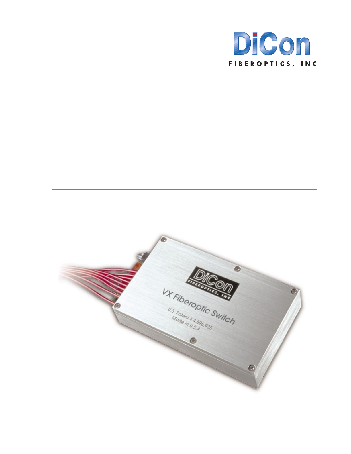
VX500
Fiberoptic Switch
Operation Manual
91500 Revision B
Page 2

2 DiCon Fiberoptics VX500 Fiberoptic Switch
Copyright © 1998 DiCon Fiberoptics, Incorporated
.
All rights reserved. Printed in the United States of America.
No part of this manual may be reproduced, in any form or by any means, electronic or
mechanical, including photocopying, without the express written permission of DiCon
Fiberoptics.
We have reason to believe that a number of the company and product names appearing
herein constitute trademarks or have been designated as such by their respective holders.
No attempt has been made to designate these words as trademarks or as registered trademarks. The inclusion, or exclusion of a word or term is not intended to affect, or express a
judgment on, the validity or legal status of the word or term as a trademark, or other proprietary ter m.
The information provided within this manual has been carefully reviewed for technical accuracy . DiCon Fiberoptics reserves the right to correct technical or typographical errors at any
time, without prior notice. In no event shall DiCon Fiberoptics be liable for errors contained
herein, or for incidental or consequential damages arising out of or related to, this document or the information contained in it.
Warranty
DiCon Fiberoptics warrants this product to be free from defects in both workmanship and
performance for a period of one year from the time of original shipment. During the warranty period, DiCon Fiberoptics will, at its option, repair or replace any material found to be
defective.
The foregoing warranty extends to all cases, except where the product has been damaged
through misuse, mishandling, inadequate maintenance, owner modification, failure to follow the installation and operating instructions provided by DiCon Fiberoptics, flood, fire or
other events outside our reasonable control.
EXCEPT AS SPECIFIED HEREIN, DICON FIBEROPTICS MAKES NO OTHER WARRANTIES, EXPRESSED OR IMPLIED, INCLUDING BUT NOT LIMITED TO, THE
IMPLIED WARRANTIES OF MERCHANTABILITY AND FITNESS FOR A PARTICULAR
PURPOSE. DICON FIBER OPTICS SHALL NO T BE LIABLE FOR D AMAGES RESULTING
FROM LOSS OF DATA, PROFITS, USE OF PRODUCTS, OR INCIDENTAL OR CONSEQUENTIAL DAMAGES. This limitation of the liability of DiCon Fiberoptics will apply regardless of the form of action whether based on contract, tort, or any other legal theory.
All Returns
Contact DiCon Fiberoptics before returning any product.
DiCon will provide a Return
Material Authorization (RMA) number and shipping instructions. No product will be
accepted for return without an RMA number clearly marked on the outside of the shipping
material.
Any unit that is returned under warranty, b ut for which evidence of misuse or mishandling is
found, will be subject to testing and processing fees, in addition to any repair costs.
DiCon Fiberoptics will cover any freight costs for returning warranty returned material to the
customer. The customer is responsible for covering any freight costs for sending materials
to DiCon Fiberoptics. The customer is responsible for all freight costs for returned materials
found to be out of warranty.
Use the original packing materials when returning material to DiCon Fiberoptics. If the original packing materials are unavailable, the customer is responsible for ensuring adequate
packing materials are used to prevent damage during shipping.
91500 Revision B
Page 3

Contents
3
Product Overview
Optical Switch Module ....................................... ...... ....... ...... ..................................... 5
VX500 Interface Board .............................................................................................. 5
Connecting to the Interface ................................................................................. 6
Reading the Status LED ............................................................................................ 6
Thermal Considerations ............................................................................................. 6
Switch Operation
Starting the Switch ..................................................................................................... 7
Resetting the Switch .................................................................................................. 7
Losing Power to the Switch ....................................................................................... 8
Selecting an Output Channel ................ ...... ....... ...... ....... ...... ....... ...... ....... ................. 8
Simplex 1
Synchronous Duplex 1
2×N Non-Blocking Configurations ................................................................... 11
2×N Blocking Configurations ........................................................................... 13
Maintaining Channel Position .................................................................................. 14
Timing Parameters .................................................................................................. 15
Calculating Switching Time ...................................................................................... 16
Switch Control
Controlling the VX500 Using a PC Printer Port ....................................................... 18
....................................................................................................... 5
........................................................................................................ 7
×
N Configurations .............................................................................. 8
×
N Configurations ....................................................... 10
........................................................................................................... 17
Specifications
Device Housing
Handling Fiberoptic Components and Cables
Handling Fiberoptic Cables ...................................................................................... 22
Storing Optical Connectors ...................................................................................... 22
Cleaning Optical Connectors ................................................................................... 22
Mating Optical Connectors ...................................................................................... 23
.................................... ...... ...... ....... ...... ....... ...... ....... ............................ 20
...................................... ................................................................... 20
................................................. 22
October 20, 1998
Page 4

4 DiCon Fiberoptics VX500 Fiberoptic Switch
91500 Revision B
Page 5
Product Overview 5
Product Overview
DiCon’s VX500 Fiberoptic Switch is a multi-channel fiberoptic switch designed for integration within products that require 1
VX500 is based on patented technology which enables precise fiber-to-fiber positioning of
either singlemode or multimode fibers.
Optical Switch Module
The VX500 optical switch module is an opto-mechanical switch that allows selection of an
individual fiber channel by means of a high-resolution stepper motor. The stepper motor
moves one or two common fibers into direct alignment with one or two of several output
fibers using DiCon’s patented moving fiber technology.
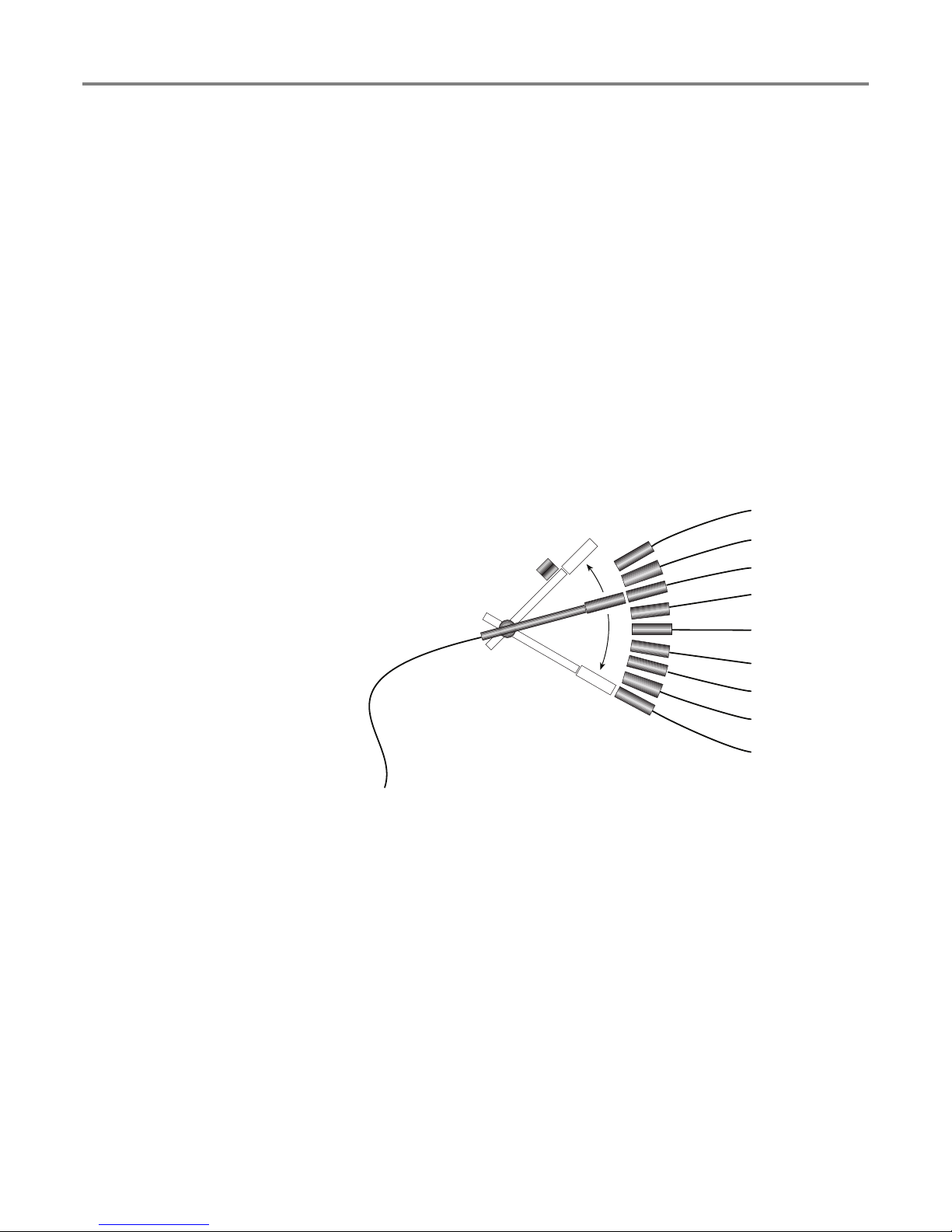
The VX500 is optically passive, operating independently of data rate, data format, and optical signal direction. Some of the terms used to describe the internal components of VX500
optical switch module are illustrated in Figure 1.
×
N or 2×N optical switch routing. The design of the
Figure 1:
The Internal Components of the VX500
Optical
Proximity
Sensor
Moving
Armature
Common
Moving Fiber
Optically Off
Channel 0
Output/Input
Fixed Fibers
Channel 1
Channel 2
Channel 3
Channel N
VX500 Interface Board
The VX500 switch module contains an electronic interface board that converts TTL input
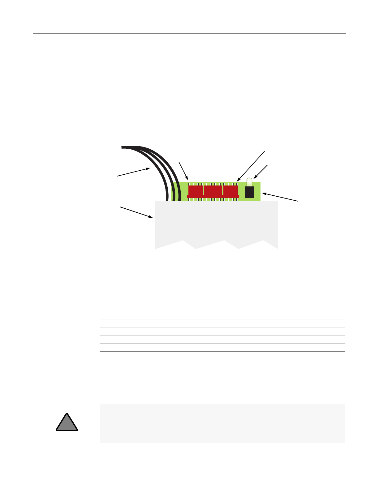
signals to the switch's optical channel position. The important components of the interface
are labeled in Figure 2.
The twelve-pin interface connector has six data inputs (RESET and <D4:D0>) and a
STROBE input as well as two status outputs. The BUSY output indicates whether the
device is busy performing an operation or ready to receive new switching instructions. The
ERROR output indicates when an error has occurred.
The board requires a constant +12 VDC supply both during switching and switch hold.
October 20, 1998
Page 6
6 DiCon Fiberoptics VX500 Fiberoptic Switch
Connecting to the Interface
The electrical connector on the DiCon VX500 Switch is a male twelve-pin 0.100-inch rightangle square-pin friction-lock header (Molex part number 22-12-2124). To mate to this connector, use a corresponding female receptacle housing (Molex part number 22-01-3127 or
equivalent) and contacts (Molex part number 08-56-0110 or equivalent). The mating connector can be obtained from Molex (Tel: (708)969-4550) or from DiCon Fiberoptics, Inc.
The maximum length of the control cable is two meters. Use shielded cable for lengths
greater than one meter.
Figure 2:
Fiber Pigtails
Switch Housing
The VX500 Interface Board (Top View)
Pin 1
Twelve-Pin Electrical Connector
LED Status Indicator
Interface Board
Reading the Status LED
The status LED provides a constant visual indication of the state of the switch. The four
possible states are defined in the following table.
Appearance State
Green Ready . Th e sw itch is oper ating properly an d ready to rece ive s witchin g instructions .
Yellow Busy. The device is performing a switch operation.
Red Error. A user error or device malfunction has occurred.
None Off. No power to the switch.
Thermal Considerations
The VX500 generates about 3 watts of heat continuously. The switch may not perform correctly if it is allowed to overheat (50°C max.). Under some circumstances, a vented air flow
may be necessary in order to keep the housing temperature within range.
Warning
!
91500 Revision B
The switch may not perform correctly if it is allowed to overheat (50°C max.). Under some
circumstances, a vented air flow may be necessary in order to keep the housing temperature
within range.
Page 7
Switch Operation 7
Switch Operation
The twelve-pin interface is used for supply power, channel selection, and status checking.
The following table defines the signals associated with each pin.
Table 1:
Pin
Number
1 GND Power Signal ground.
2 GND Power Power ground.
3 D0 Input The D0 input is the LSB of the channel address.
4 D1 Input The D1 input is bit 1 of the channel address.
5 D2 Input The D2 input is bit 2 of the channel address.
6 D3 Input The D3 input is bit 3 of the channel address.
7 D4 Input The D4 input is the MSB of the channel address.
8 STROBE Input The STROBE input is a falling-edge-trigger clock signal.
9 BUSY Output The BUSY output is high when the switch is busy, and low
10 ERROR Output The ERROR output is low during normal operation. A high
11 RESET Input Set RESET to low to return the switch to the reset position,
12 POWER Power Power supply input (+12VDC ±5%, 300mA max.)
Interface Pin Assignments
Signal
Name
Signal
Type Description
when the switch is ready.
ERROR output indicates that the requested channel is out of
range (user error) or that a steppe r motor or pro ximity s witch
error has occurred (device malfunction).
and to high to choose a different output channel.
Starting th e Switch
T o start the switch, apply power (+12 VDC ±5%, 300mA max.) to the POWER line. A stable
voltage with less than 10mV RMS ripple is recommended.
The switch requires a 970-ms initialization period upon power up while the switch armature
returns to reset position. Do not apply TTL input to the data lines (D0, D1, D2, D3, D4,
STROBE, and RESET) during initialization. Switch control may lock up if data is applied
during initialization. If the switch locks up, cycle the supply power and restart the switch.
Warning
!
Applying TTL-level signals to the data lines before or during switch initialization may lock up
switch con trol. Do n ot apply TTL-lev el sign als to the data line s until p ower has been applied to the
POWER input for 970ms.
During the 970-ms initialization period, the BUSY and ERROR outputs as well as the optical outputs are invalid.
Resetting the Switch
When the VX500 is in the reset position (also called the park position, channel zero, or optical off), there is no optical connection to any output channel. Set the switch to the reset
position to prevent optical data from passing through the switch, or to reset the stepper
motor. During a reset operation, optical noise may appear on various output channels as
the armature rotates.
October 20, 1998
Page 8

8 DiCon Fiberoptics VX500 Fiberoptic Switch
One way to reset the switch is to cycle the supply power to the switch. The switch returns
to the reset position following the initial application of power to the POWER pin (see “Starting the Switch” on page 7).
To return the switch to the reset position without interrupting the supply power, set the
RESET input to low and apply a STROBE pulse. The RESET input is latched by the falling
edge of the STROBE signal, respecting hold, setup, and pulse width constraints (see
Table 6). The BUSY output remains high until the reset operation is complete and the
device is ready to receive additional instructions.
Losing Power to the Switch
If the supply power is interrupted the switch
does not
latch in its current position. Instead,
it loses direct fiber-to-fiber alignment, breaking the optical connection. When supply power
is restored the switch automatically restarts, returning to the reset position.
Selecting an Output Channel
To choose a specific channel, set the RESET input to high, set the channel address inputs
(<D4:D0>) to the appropriate value (see Tables 2, 3, 4, and 5), and apply a STROBE pulse.
The inputs are latched by the falling edge of the STROBE signal, respecting hold, setup,
and pulse width constraints (see Table 6). The BUSY output will go high until the STROBE
pulse has ended, the switch operation is complete, and the device is ready to receive additional instructions. Note that the BUSY signal will remain high until the end of the STROBE
pulse, even if the switch operation is complete and the optical connection is stable.
If the latched value of the channel address (<D4:D0>) is the same as the previous latched
value, the BUSY signal will go high for 60–80ms even though there is no switch movement.
If the latched value of the channel address (<D4:D0>) indicates an out-of-range position,
the BUSY and ERROR signals will go high for 60–80ms.
The following sections list the switch channel number associated with each data-input setting for simplex 1
switches, respectively.
Simplex 1
×
N, synchronous duplex 1×N, 2×N blocking, and 2×N non-blocking
N Configurations
×
The relationship between the optical inputs and outputs in a VX500 simplex 1
shown in Figure 3.
Figure 3:
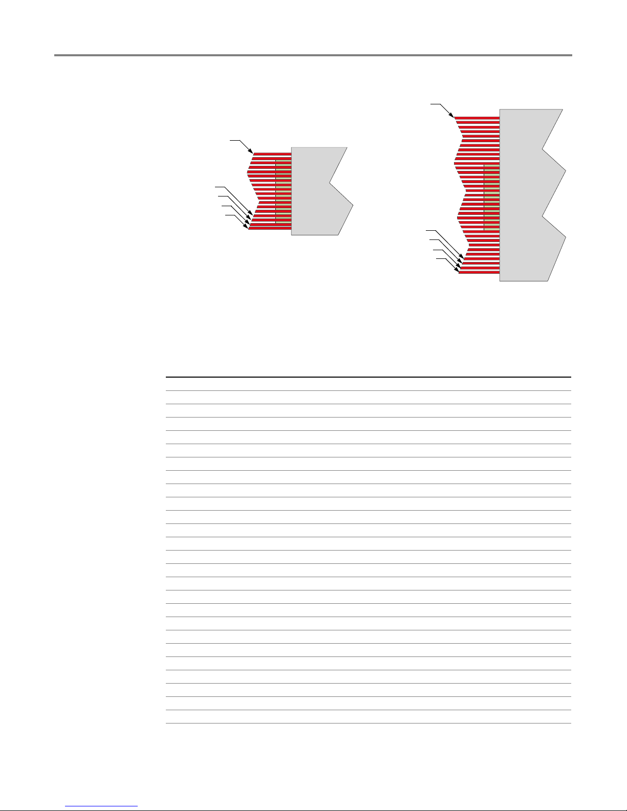
The arrangement of the fiber pigtails on a VX500 1×N switch is shown in Figure 4. The left
diagram applies to switch units with up to 16 output channels. The right diagram applies to
units with 17–32 output channels.
91500 Revision B
Simplex 1
×
N Switch Configuration
1
×
N switch is
0
1
2
3
N
Page 9
Switch Operation 9
COMMON
CHANNEL 1
CHANNEL 2
CHANNEL 3
CHANNEL N
COMMON
CHANNEL 1
CHANNEL 2
CHANNEL 3
CHANNEL N
Figure 4:
To select the output channel of a simplex 1×N switch with up to 32 output channels, set the
five channel address inputs (<D4:D0>) and the RESET input as indicated in Table 2, then
strobe the device.
Table 2:
RESET D4 D3 D2 D1 D0 Active Channel
0xxxxx0 reset
1000001
1000012
1000103
1000114
1001005
1001016
1001107
1001118
1010009
10100110
10101011
10101112
10110013
10110114
10111015
10111116
11000017
11000118
11001019
11001120
11010021
11010122
11011023
11011124
11100025
11100126
Control Codes For Simplex 1
Simplex 1
×
N Channel Order (Top View)
×
N Configurations
October 20, 1998
Page 10
10 DiCon Fiberoptics VX500 Fiberoptic Switch
COMMON 1
COMMON 2
CHANNEL 1-1
CHANNEL 1-2
CHANNEL N-2
COMMON 1
COMMON 2
CHANNEL 1-1
CHANNEL 1-2
CHANNEL N-2
Table 2:
Control Codes For Simplex 1
×
N Configurations (Continued)
RESET D4 D3 D2 D1 D0 Active Channel
11101027
11101128
11110029
11110130
11111031
11111132
Synchronous Duplex 1×N Configurations
The relationship between the optical inputs and outputs in a VX500 synchronous duplex
×
1
N switch is shown in Figure 5.
Figure 5:
Synchronous Duplex 1
1
2
×
N Switch Configuration
0
0
1-1
1-2
2-1
2-2
N-1
N-2
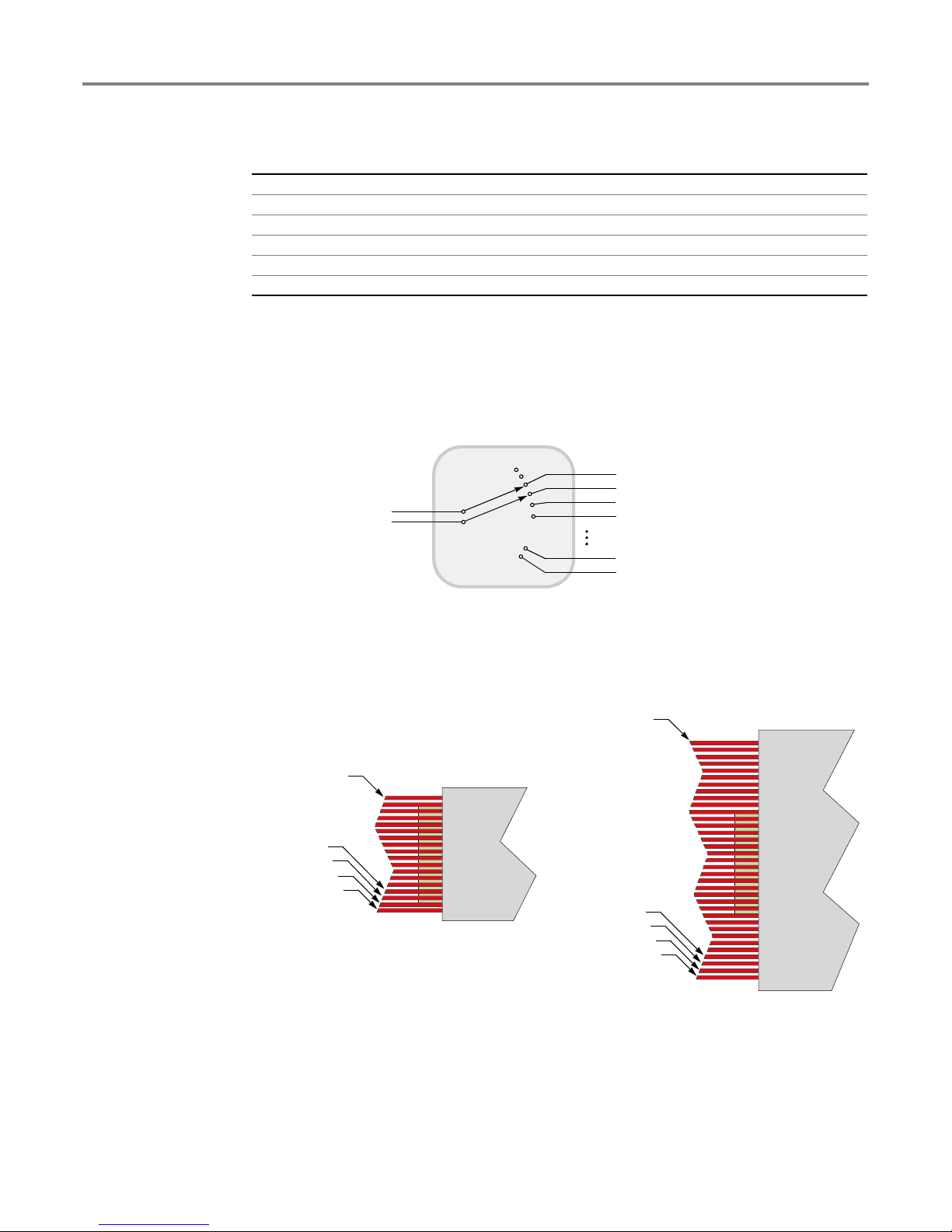
The arrangement of the fiber pigtails on a VX500 synchronous duplex 1×N switch is shown
in Figure 6. The left diagram applies to switch units with up to 16 output channels (1
The right diagram applies to units with 18–32 output channels (1
Figure 6:
Synchronous Duplex 1
×
N Channel Order (Top View)
×
9 to 1×16).
×
8).
91500 Revision B
Page 11
Switch Operation 11
To select the output channel of a simplex 1×N switch with up to 50 output channels (1×25),
set the five channel address inputs (<D4:D0>) and the RESET input as indicated in
Table 3, then strobe the device.
Table 3:
Control Codes for Synchronous Duplex 1
RESET D4 D3 D2 D1 D0
×
N Configurations
Common 1
Active Channel
Common 2
Active Channel
0xxxxx0 reset 0 reset
1000001-1 1-2
1000012-1 2-2
1000103-1 3-2
1000114-1 4-2
1001005-1 5-2
1001016-1 6-2
1001107-1 7-2
1001118-1 8-2
1010009-1 9-2
10100110-1 10-2
10101011-1 11-2
10101112-1 12-2
10110013-1 13-2
10110114-1 14-2
10111015-1 15-2
10111116-1 16-2
11000017-1 17-2
11000118-1 18-2
11001019-1 19-2
11001120-1 20-2
11010021-1 21-2
11010122-1 22-2
11011023-1 23-2
11011124-1 24-2
11100025-1 25-2
2
N Non-Blocking Configurations
×
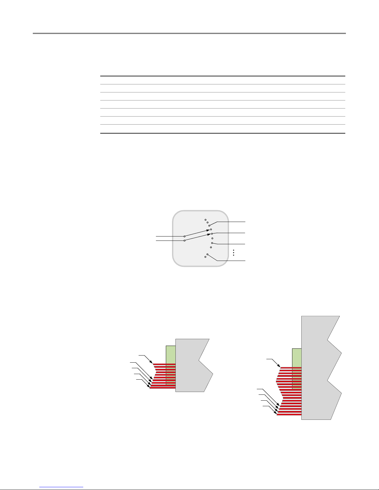
The relationship between the optical inputs and outputs of a VX500 2
switch is shown in Figure 7.
Figure 7:
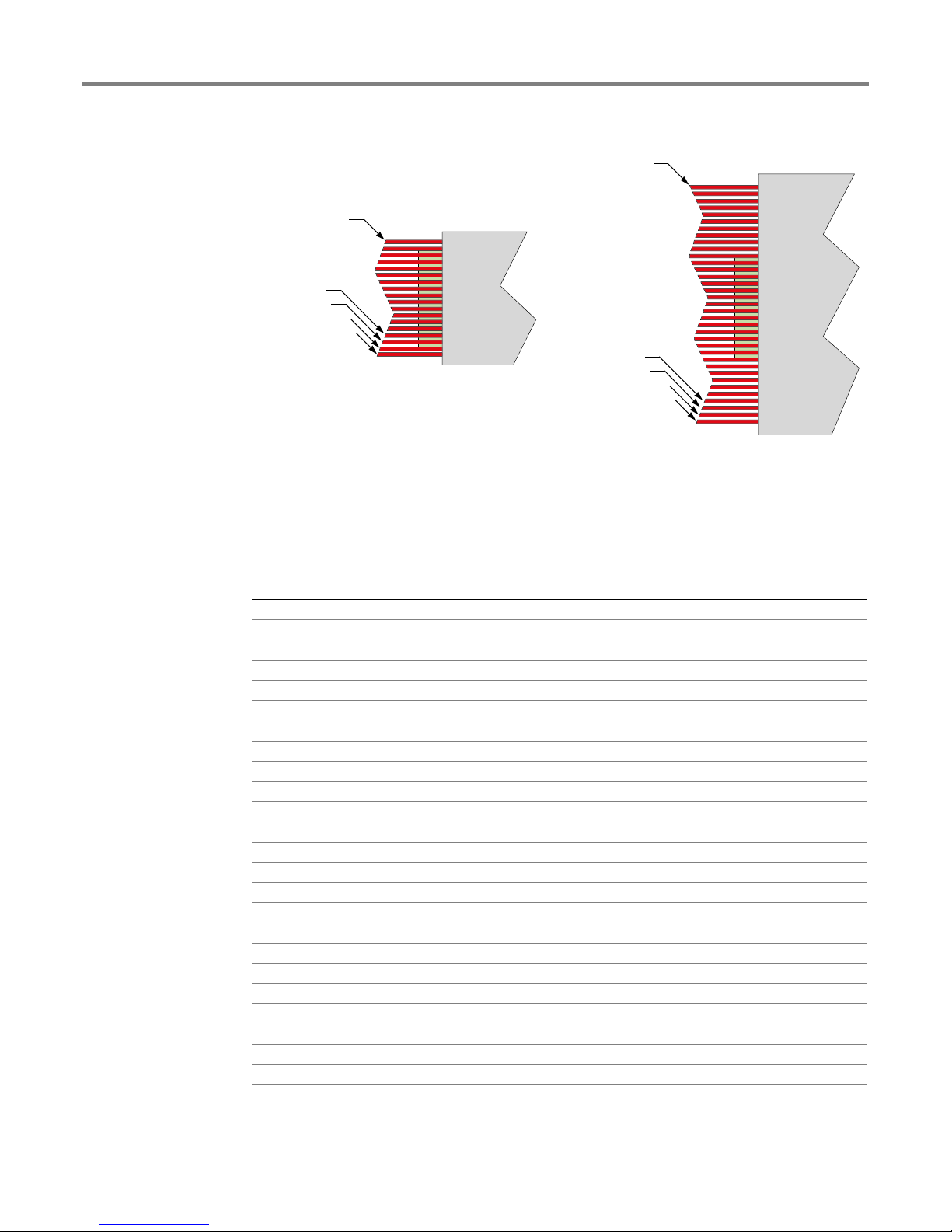
The arrangement of the fiber pigtails on a VX500 2×N non-blocking switch is shown in Figure 8. The left diagram applies to switch units with up to 16 output channels. The right diagram applies to units with 17–32 output channels.
×
2
N Non-Blocking Switch Configuration
-1
0
2
1
block
×
N non-blocking
1
2
3
N
October 20, 1998
Page 12
12 DiCon Fiberoptics VX500 Fiberoptic Switch
COMMON 1
COMMON 2
CHANNEL 1
CHANNEL 2
CHANNEL N
COMMON 1
COMMON 2
CHANNEL 1
CHANNEL 2
CHANNEL N
91500 Revision B
Figure 8:
×
2
N Non-Blocking Channel Order (Top View)
To select the output channel of a 2×N non-blocking switch with up to 32 output channels,
set the five channel address inputs (<D4:D0>) and the RESET input as indicated in
Table 4, then strobe the device.
Table 4:
Control Codes For 2
RESET D4 D3 D2 D1 D0
0xxxxx0 reset -1 reset
1000001 0 block
1000012 1
1000103 2
1000114 3
1001005 4
1001016 5
1001107 6
1001118 7
1010009 8
10100110 9
10101011 10
10101112 11
10110013 12
10110114 13
10111015 14
10111116 15
11000017 16
11000118 17
11001019 18
11001120 19
11010021 20
11010122 21
11011023 22
11011124 23
11100025 24
×
N Non-Blocking Configurations
Common 1
Active Channel
Common 2
Active Channel
Page 13
Switch Operation 13
COMMON 1
COMMON 2
CHANNEL 1
CHANNEL 2
CHANNEL N
COMMON 1
COMMON 2
CHANNEL 1
CHANNEL 2
CHANNEL N
Table 4:
Control Codes For 2
RESET D4 D3 D2 D1 D0
×
N Non-Blocking Configurations (Continued)
Common 1
Active Channel
Common 2
Active Channel
11100126 25
11101027 26
11101128 27
11110029 28
11110130 29
11111031 30
111111
a. When the channel address is set to N (the highest input channel), Common 1 is blocked and
Common 2 is aligned with Channel N.
block
a
31
2×N Blocking Configurations
×
The relationship between the optical inputs and outputs of the VX500 2
N blocking switch
is shown in Figure 9.
Figure 9:
×
2
N Blocking Switch Configuration
2
1
-1
0
block
block
block
1
2
3
The arrangement of the fiber pigtails on a VX500 2×N blocking switch is shown in
Figure 10. The left figure applies to switch units with up to 8 output channels. The right figure applies to units with 9–16 output channels.
Figure 10:
block
×
2
N Blocking Channel Order (Top View)
N
October 20, 1998
Page 14

14 DiCon Fiberoptics VX500 Fiberoptic Switch
T o select the output channel of a 2×N blocking switch with up to 16 output channels, set the
five channel address inputs (<D4:D0>) and the RESET input as indicated in Table 5, then
strobe the device.
Table 5:
RESET D4 D3 D2 D1 D0
0xxxxx0 reset -1 reset
1000001 0 block
100001block 1
1000102 block
100011block 2
1001003 block
100101block 3
1001104 block
100111block 4
1010005 block
101001block 5
1010106 block
101011block 6
1011007 block
101101block 7
1011108 block
101111block 8
1100009 block
110001block 9
11001010 block
110011block 10
11010011 block
110101block 11
11011012 block
110111block 12
11100013 block
111001block 13
11101014 block
111011block 14
11110015 block
111101block 15
11111016 block
111111block 16
Control Codes For 2
×
N Blocking Configurations
Common 1
Output Channel
Common 2
Output Channel
Maintaining Channel Position
To maintain channel position, keep the STROBE signal high and do not interrupt supply
power.
91500 Revision B
Page 15
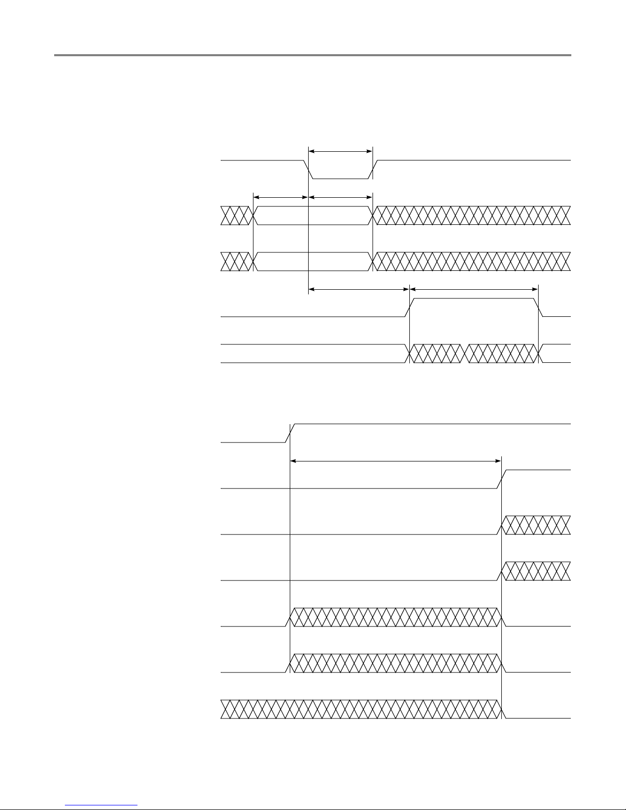
Timing Parameters
STROBE
BUSY
OPTICAL
OUTPUT
<D4:D0>
RESET
Tstb
ThTsu
Tbsy Tsw
POWER
RESET
BUSY
STROBE
<D4:D0>
Tpwr
ERROR
OPTICAL
OUTPUT
Switch Operation 15
Figure 11:
Figure 12:
VX500 Switch Timing
VX500 Power-Up Timing
October 20, 1998
Page 16

16 DiCon Fiberoptics VX500 Fiberoptic Switch
Table 6:
Parameter Description Min. Max. Units
Tsu Setup time. The channel address (<D4:D0>) and
Th Hold time. The channel address (<D4:D0>) and
Tstb
Tbsy STROBE low to BUSY high. During this period the
Tsw Switching time. During this period there may be
Tpwr P o wer-up dela y. The switch may loc k up if TTL-le v el
a. DiCon recommends a low pulse width of 1 µsec to 10 µs.
VX500 Timing Parameters
RESET inputs must remain stable preceding the
falling edge of STROBE.
RESET inputs must remain stable following the
falling edge of STROBE.
STROBE pulse width.
switch maintains a valid connection to the previous
output channel.
invalid optical transmission on all channels.
signals are applied to the data inputs during this
period. Status and optical outputs are unreliable.
a
100 — ns
150 — ns
150
— 500 ns
— 300 +
— 970 ms
6 × 10
(16 × N)
7
ns
ms
Calculating Switching Time
The time period that begins at the falling edge of the STROBE signal and ends upon completion of the switching operation can be divided into three constituent periods. The first
period begins when STROBE goes low and ends when BUSY goes high. During this period
(500ns max.), the optical connection for the previous channel selection remains valid.
The second period begins when BUSY goes high and the switch armature begins to move.
It ends when the armature reaches the specified output channel. The period lasts for 16ms
per switched channel, including blocked and duplex channels. During this period, optical output is invalid; optical noise may appear on various output channels as the armature rotates.
The final period is called the debounce period. It ends when the armature is steady, the
switch has established a valid optical connection, and BUSY goes low. The debounce
period lasts for 300ms.
1
Switching time is the sum of final two periods. For example, consider the calculation of total
switching time for the following two scenarios:
Switch From Channel 15 To Channel 1 (Simplex 1×N Switch)
(14 × 16 ms) + 300 ms = 524 ms
Switch From Channel 2 To Channel 6 (2×N Blocking Switch)
(8 × 16 ms) + 300 ms = 428 ms
Additionally, there are two special cases for calculating switching time. First, if a STROBE
pulse is applied with no change in the latched value of the channel address (<D4:D0>), the
BUSY line will go high for 60–80ms. Second, if a reset instruction is given twice in a row,
the BUSY line will go high for 410ms max. For example, consider the total switching time
for the following two scenarios:
Switch From Channel 3 To Channel 3
60–80ms
Switch From Channel 0 To Channel 0
410ms max.
1. The BUSY line will remain high until the end of the STROBE pulse, even if the switch operation is complete
and the optical connection is stable.
91500 Revision B
Page 17
Switch Control 17
Switch Control
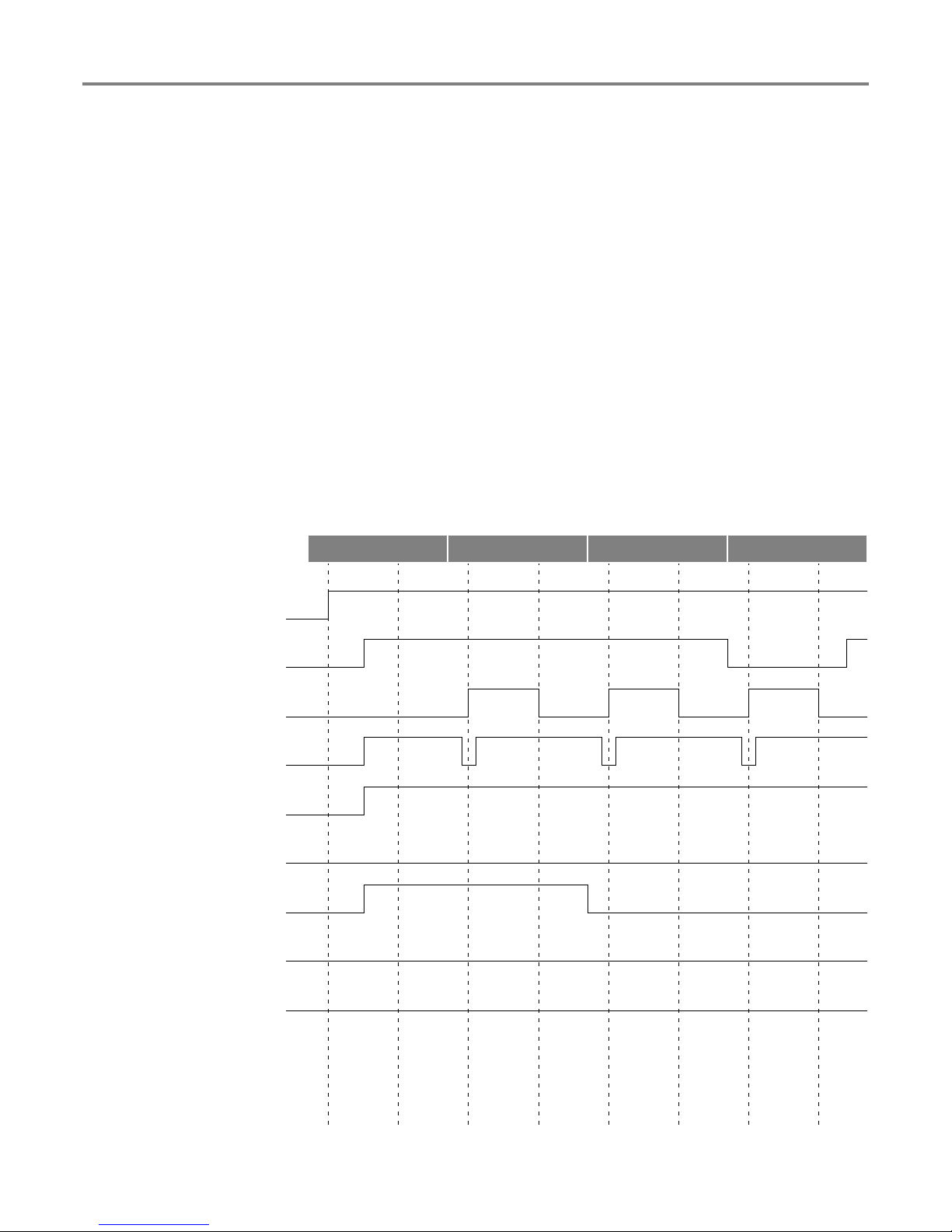
Figure 13 illustrates the following sample control sequence for a 1×N simplex switch.
1. Following power-up, the switch returns to reset position. After the initialization period,
the device is ready to rece ive instructions.
2. The user brings STROBE high, brings RESET high to enable channel selection, and
sets the desired channel address. The user applies a strobe pulse, sending the BUSY
line high while the switch moves into alignment with channel 6. The BUSY line returns
to low when the switch operation is complete and the device is ready to accept new
instructions.
3. With the RESET line still high, the user changes the channel address and applies
another STROBE pulse, the BUSY line goes high while the switch moves into alignment with channel 2.
4. Finally, the user brings RESET low and applies another STROBE pulse. The device
disregards the channel address inputs. The BUSY line goes high while the switch
returns to the reset position.
Figure 13:
+12 VDC
RESET
BUSY
STROBE
D0
D1
D2
D3
Sample Control Sequence
1234
D4
SWITCH
FUNCTION
OUTPUT
CHANNEL
Off
Not
Valid
Power Up
Auto Reset
Not
Valid
Ready Ready
Channel 0
Reset
Read
00101
Not
Valid
Ready
Channel 6
Read
00001
Not
Valid
Channel 2
Reset
Request
Not
Valid
Ready
Channel
Reset
October 20, 1998
Page 18
18 DiCon Fiberoptics VX500 Fiberoptic Switch
Controlling the VX500 Using a PC Printer Port
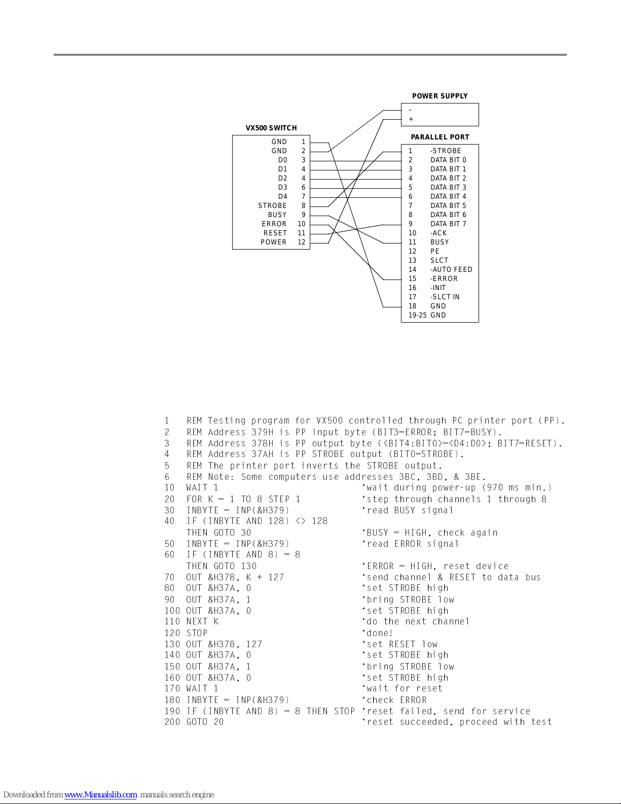
It is possible to control the VX500 switch by connecting the interface board to a PC printer
port and a power supply (+12VDC ±5%, 300 mA max.). The printer port has a 25-pin, Dshell connector. The recommended cable configuration for connection to the printer port is
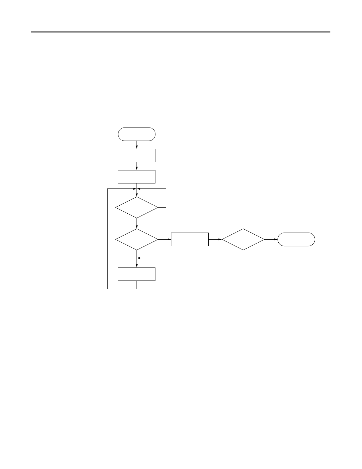
shown in Figure 15. The basic control flow for the VX500 is illustrated in Figure 14. For specific procedures for sending reset and switch instructions, see “Switch Operation” on page
7, “Timing Parameters” on page 15, and “Selecting an Output Channel” on page 8.
Figure 14:
Switch Control Flow
START
Power-Up
+12 VDC
Wait fo r
970 ms.
Is the
BUSY signal
high?
No
Is the
ERROR signal
high?
No
Send switch
instruction
Yes
Yes
Send reset
instruction
Is the
ERROR signal
still high?
No
Yes
STOP!
Send for service
91500 Revision B
Page 19
Switch Control 19
Figure 15:
Parallel Port Line Assignments
VX500 SWITCH
GND 1
GND 2
D0 3
D1 4
D2 4
D3 6
D4 7
STROBE 8
BUSY 9
ERROR 10
RESET 11
POWER 12
POWER SUPPLY
–
+
PARALLEL PORT
1 -STROBE
2 DATA BIT 0
3 DATA BIT 1
4 DATA BIT 2
5 DATA BIT 3
6 DATA BIT 4
7 DATA BIT 5
8 DATA BIT 6
9 DATA BIT 7
10 -ACK
11 BUSY
12 PE
13 SLCT
14 -AUTO FEED
15 -ERROR
16 -INIT
17 -SLCT IN
18 GND
19-25 GND
The following BASIC program can be used to control the VX500 from a PC printer port. The
program switches channel-by-channel from channel 1 through channel 8. If an error is
encountered, the program resets the switch. If the error persists, the program exits. The
program expects the VX500 to be connected to the printer port as outlined in Figure 15.
Depending on the speed of your PC, you may have to insert a delay after the STROBE low
commands (lines 90, 150) in order to satisfy minimum pulse width constraints.
1 REM Testing program for VX500 controlled through PC printer port (PP).
2 REM Address 379H is PP input byte (BIT3=ERROR; BIT7=BUSY).
3 REM Address 378H is PP output byte (<BIT4:BIT0>=<D4:D0>; BIT7=RESET).
4 REM Address 37AH is PP STROBE output (BIT0=STROBE).
5 REM The printer port inverts the STROBE output.
6 REM Note: Some computers use addresses 3BC, 3BD, & 3BE.
10 WAIT 1 wait during power-up (970 ms min.)
20 FOR K = 1 TO 8 STEP 1 step through channels 1 through 8
30 INBYTE = INP(&H379) read BUSY signal
40 IF (INBYTE AND 128) <> 128
THEN GOTO 30 BUSY = HIGH, check again
50 INBYTE = INP(&H379) read ERROR signal
60 IF (INBYTE AND 8) = 8
THEN GOTO 130 ERROR = HIGH, reset device
70 OUT &H378, K + 127 send channel & RESET to data bus
80 OUT &H37A, 0 set STROBE high
90 OUT &H37A, 1 bring STROBE low
100 OUT &H37A, 0 set STROBE high
110 NEXT K do the next channel
120 STOP done!
130 OUT &H378, 127 set RESET low
140 OUT &H37A, 0 set STROBE high
150 OUT &H37A, 1 bring STROBE low
160 OUT &H37A, 0 set STROBE high
170 WAIT 1 wait for reset
180 INBYTE = INP(&H379) check ERROR
190 IF (INBYTE AND 8) = 8 THEN STOP reset failed, send for service
200 GOTO 20 reset succeeded, proceed with test
October 20, 1998
Page 20

20 DiCon Fiberoptics VX500 Fiberoptic Switch
Specifications
Table 7:
Performanc e Spe ci ficat ion s
Parameter Minimum Typical Maximum Units
Optical
insertion loss
back-reflection (singlemode fiber)
back-reflection (multimode fiber)
switching time
a
b
d
—0.61.2dB
c
—-60-55dB
c
—-20—dB
— — 300+(16×N) ms
isolation — — -80 dB
durability 10 million cycles
repeatability
f
PDL
e
— — ±0.03 dB
——0.05dB
wavelength range 780 — 1650 nm
Environmental
operating tempera ture : 0 — 50 °C
storage temperature -20 — 70 °C
humidity 40°C / 90% RH / 5 days —
a. All specifications referenced without connectors.
b. Measured at 23±5°C.
c. Bas ed on standard 1-meter pigtail length.
d. Based on BUSY output pulse. Actual optical switching time may be faster.
e. Sequential repeatability for 100 cycles at constant temperature after warm-up.
f. Measured at 1550 nm.
Device Housing
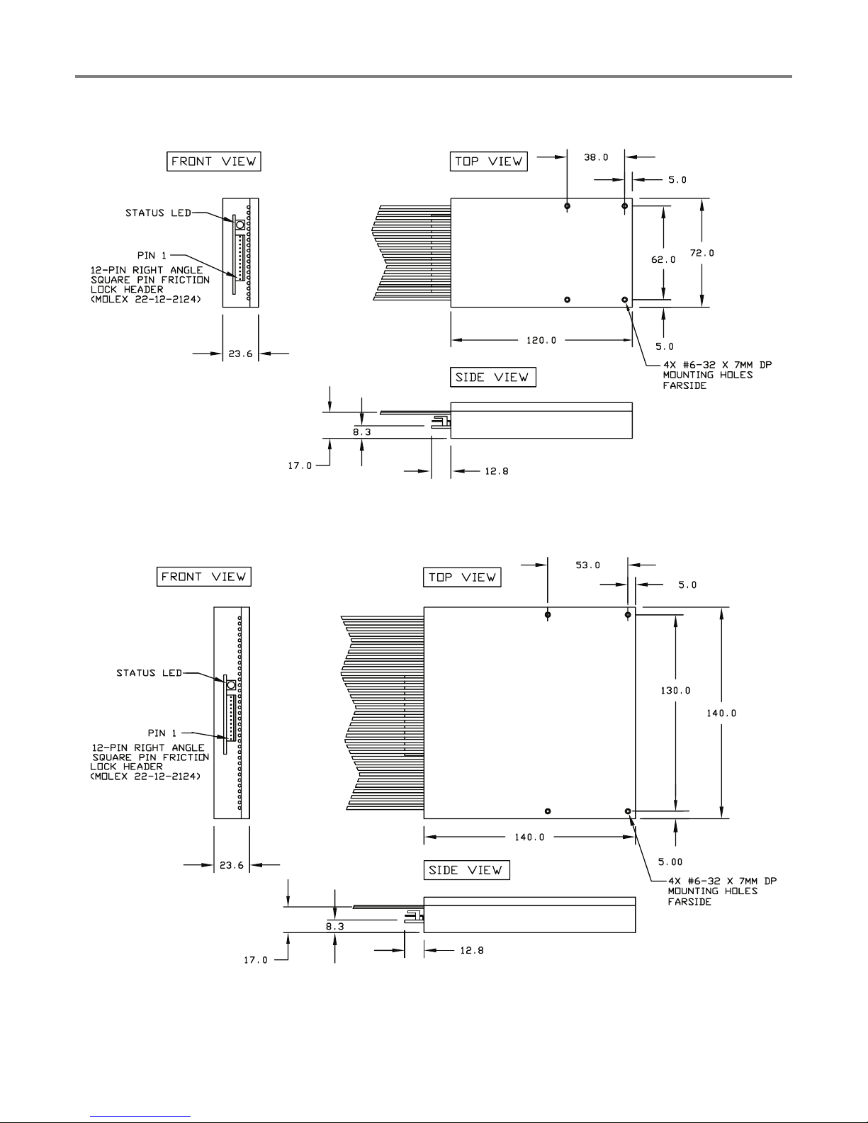
The VX500 Switch is suitable for mounting on a panel or printed circuit board. Four mounting holes are provided. Do not remove the housing cover. Removal of housing cover voids
warranty.
Table 8:
Parameter
Height 23.6 [0.93] 23.6 [0.93] mm [in.]
Width 72.0 [2.83] 140.0 [5.51] mm [in.]
Depth 120.0 [4.72] 140.0 [5.51] mm [in.]
Weight
a. Including blocked and duplex channels
b. Actual weight depends upon switch configuration.
Housing Dimensions
Size 1
1 to 17 Channels
b
0.4 [0.8] 0.9 [2.1] kg [lb.]
a
18 to 32 Channels
a
Units
Size 2
91500 Revision B
Page 21
Device Housing 21
Figure 16:
Figure 17:
VX500 Chassis Size 1 Housing
VX500 Chassis Size 2 Housing
October 20, 1998
Page 22
22 DiCon Fiberoptics VX500 Fiberoptic Switch
Handling Fiberoptic Components and Cables
Handling Fiberoptic Cables
Your switch may come with fiber pigtail outputs. Treat cables with care to avoid cable damage and minimize optical loss. The minimum bend radius for most optical cables is 35mm.
Never bend an optical cable more sharply than this specification. Optical performance will
degrade and the cable may break.
• Avoid bending the optical cable near a cable strain relief boot. Bending an optical cable
near a strain relief boot is one of the easiest ways to permanently damage the optical
fiber.
• Avoid bending the optical cable over a sharp edge.
• Avoid using cable tie wraps to hold optical cable. Tie wraps when tightened can create
micro-bends or break an optical cable. Microbends can cause a dramatic reduction in
optical performance.
• Do not pull on the bare fiber as this can break the fiber inside the component.
• Avoid using soldering irons near optical cable. Accidental damage can easily occur
when an soldering iron is used near an optical cable. In addition, solder splatter can contaminate and permanently damage optical fiber connectors.
• In order to obtain the most stable, repeatable optical performance, immobilize optical
cables using wide pieces of tape or some form of mechanical cushion after the optical
cables have been connected.
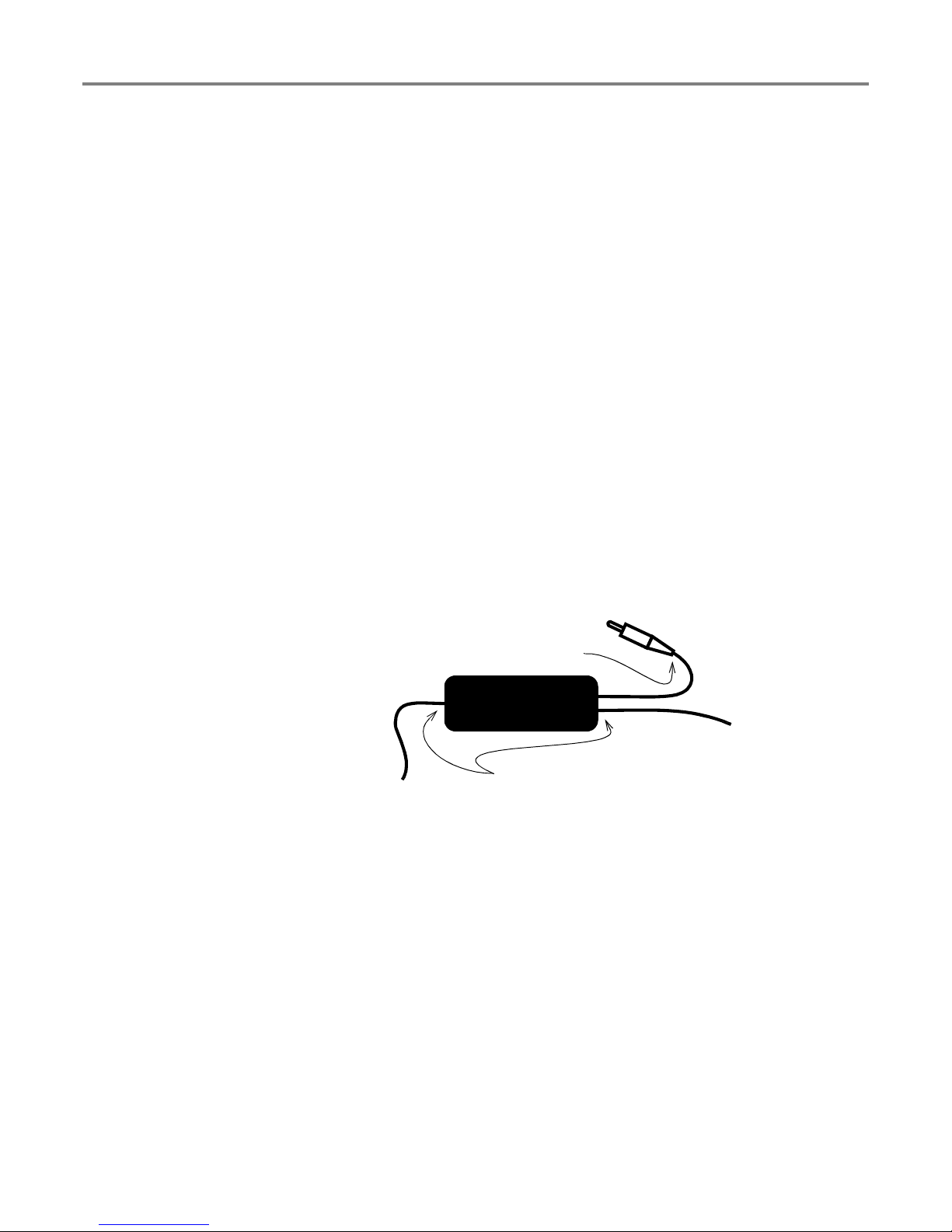
Do not bend the fibers at the
exit of the connector strain
relief boot. The fiber will
break if stressed at this point.
FIBEROPTIC
COMPONENT
Do not bend the fibers at the
exits of the switch housing.
The fiber will break if
stressed at these points.
CONNECTOR
FIBER
PIGTAILS
Storing Optical Connectors
All switches are shipped with dust caps in place covering all optical connectors. Optical
connectors should remain covered at all times when the instrument is not in use.
Cleaning Optical Connectors
Clean any exposed connector using a cleaning kit supplied by the connector manufacturer
or high-grade isopropyl alcohol and a cotton swab. To clean with alcohol and a swab, dab
the tip of a cotton swab in alcohol and then shake off any excess alcohol. The tip should be
not
moist,
around the connector ferrule. Either allow the connector a minute to dry, or blow dry the
connector using compressed air. Be careful when using compressed air because improper
use may deposit a spray residue.
dripping wet. Stroke the swab tip gently across the surface of the connector and
91500 Revision B
Page 23

Handling Fiberoptic Components and Cables 23
Mating Optical Connectors
• Clean both connectors prior to mating. Any small particles trapped during the mating
process can permanently damage the connector.
• Insert the appropriate connector ferrule into the adapter smoothly. Do not allow the fiber
tip to contact any surface. If the tip accidentally contacts a surface before mating,
Re-clean the connector and try again.
• Tighten the connector until it is finger tight, or to the torque specified by the connector
manufacturer. Do not over-tighten the connector as this can lead to optical loss and connector damage.
• Check the optical insertion loss. If the loss is unacceptable, Remove the connector, re-
clean both ends of the mate, and reconnect. You may have to repeat this process several times before a low-loss connection is made.
• After you make the connection, monitor the stability of the optical throughput for a few
minutes. Optical power trending (slowly increasing or decreasing) is caused by the slow
evaporation of alcohol trapped in the connection. Continue to monitor optical power until
it stabilizes. If the loss is unacceptable, reclean the connectors and start again.
stop
.
October 20, 1998
Page 24

DiCon Fiberoptics, Inc.
1331 Eighth Street
Berkeley, CA 94710 USA
W orld Wide Web
www.diconfiberoptics.com
 Loading...