

Page 1

SERVICE MANUAL
HIGH RESOLUTION DISPLAY MONITOR
Diamond Pro 2060u
NSZ2107STTUW
NEC-MITSUBISHI ELECTRIC VISUAL SYSTEMS CORPORATION
MARCH 2001
CBB-S5730
Page 2

iii
Contents
1. Circuit description ...................................................................................................................... 1-1
1.1 Power block ......................................................................................................................... 1-1
1.1.1 Outline ...................................................................................................................... 1-1
1.1.2 Rectifying circuit ....................................................................................................... 1-1
1.1.3 Surge current suppression ...................................................................................... 1-1
1.1.4 Higher harmonic circuit ............................................................................................ 1-2
1.1.5 Sub power circuit ...................................................................................................... 1-4
1.1.6 Main power circuit..................................................................................................... 1-4
1.1.7 Degaussing circuit .................................................................................................... 1-7
1.1.8 Power management circuit ...................................................................................... 1-7
1.1.9 Protective circuit ....................................................................................................... 1-7
1.2 Horizontal deflection block ................................................................................................ 1-12
1.2.1 Distortion compensation waveform generating circuit ........................................ 1-13
1.2.2 Deflection current compensation circuit ................................................................ 1-22
1.3 Vertical output block ........................................................................................................... 1-24
1.4 High voltage block .............................................................................................................. 1-25
1.4.1 High voltage control circuit...................................................................................... 1-25
1.4.2 Protective function circuit ........................................................................................ 1-25
1.4.3 DBF (Dynamic Beam Focus) circuit ....................................................................... 1-27
1.5 CRT compensation block ................................................................................................... 1-29
1.5.1 Rotation circuit .......................................................................................................... 1-29
1.5.2 Corner purity circuit .................................................................................................. 1-29
1.5.3 Earth magnetism cancel circuit .............................................................................. 1-30
1.5.4 Digital dynamic convergence clear (DDCC) circuit ............................................. 1-31
1.6 Control block........................................................................................................................ 1-38
1.6.1 Sync. signal process ................................................................................................ 1-38
1.6.2 Front button ............................................................................................................... 1-38
1.6.3 I2C bus control .......................................................................................................... 1-38
1.6.4 Power control ............................................................................................................ 1-38
1.6.5 ABL, Beam protector ................................................................................................ 1-39
1.6.6 CRT support .............................................................................................................. 1-39
1.6.7 High voltage control ................................................................................................. 1-39
1.6.8 Display Data Channel .............................................................................................. 1-40
1.6.9 LED ............................................................................................................................. 1-40
1.6.10 Clamp pulse ............................................................................................................. 1-41
1.6.11 SPARK ...................................................................................................................... 1-41
1.6.12 Avoidance operation during input SYNC switching ........................................... 1-41
1.6.13 CS switch and vertical linearity switch ............................................................... 1-41
Page 3

iv
1.6.14 H/W RESET ............................................................................................................. 1-41
1.6.15 Oscillation circuit..................................................................................................... 1-42
1.6.16 I/O expander ............................................................................................................ 1-42
1.7 Software ................................................................................................................................ 1-42
1.7.1 Outline ...................................................................................................................... 1-42
1.7.2 Frequency variation detection function ................................................................. 1-42
1.7.3 Memory of user timing ............................................................................................. 1-43
1.7.4 Picture adjustment .................................................................................................... 1-43
1.7.5 Power management .................................................................................................. 1-43
1.7.6 OSD display at NO SYNC ....................................................................................... 1-44
1.7.7 LED display ................................................................................................................ 1-44
1.7.8 Status memory to EEPROM .................................................................................... 1-45
1.8 Deflection processor block ................................................................................................ 1-46
1.8.1 Outline ...................................................................................................................... 1-46
1.8.2 Vertical deflection waveform generating circuit ................................................... 1-46
1.8.3 Horizontal deflection drive waveform generating circuit..................................... 1-47
1.8.4 Distortion compensation waveform generating circuit ........................................ 1-47
1.8.5 DBF compensation waveform generating circuit ................................................. 1-47
1.8.6 Convergence compensation waveform generating circuit .................................. 1-48
1.8.7 Blanking waveform generating circuit.................................................................... 1-48
1.8.8 Moire canceling circuit ............................................................................................. 1-48
1.8.9 Distortion compensating operation ........................................................................ 1-50
1.9 Video block .......................................................................................................................... 1-51
1.9.1 Picture signal amplifier circuit ................................................................................ 1-51
1.9.2 Cut-off circuit ............................................................................................................. 1-51
1.9.3 2-input change over circuit and synchronizing signal circuit ............................. 1-54
1.9.4 On Screen Display circuit ........................................................................................ 1-56
1.9.5 AUTO SIZE function ................................................................................................. 1-57
1.10 USB circuit ......................................................................................................................... 1-59
1.10.1 Outline ...................................................................................................................... 1-59
1.10.2 USB downstream power supply............................................................................ 1-59
1.10.3 HUB controller power output................................................................................. 1-59
1.11 Wave form of main circuit voltage .................................................................................. 1-60
Page 4

v
2. Adjustment procedure ............................................................................................................... 2-1
2.1 Measuring instruments ....................................................................................................... 2-1
2.2 Preparatory inspections ..................................................................................................... 2-1
2.3 Names of each monitor part .............................................................................................. 2-2
2.3.1 Configuration of front control panel ....................................................................... 2-2
2.3.2 Configuration of rear input connector .................................................................... 2-2
2.3.3 OSD display matrix ................................................................................................... 2-3
2.3.3.1 User mode ................................................................................................... 2-3
2.3.3.2 Factory mode .............................................................................................. 2-4
2.4 Adjustment ........................................................................................................................... 2-6
2.4.1 How to select the factory adjustment (FACTORY) mode ................................... 2-6
2.4.1.1 Selecting with front panel switches ......................................................... 2-6
2.4.2 Adjustments before aging ........................................................................................ 2-6
2.4.2.1 Adjusting the high voltage and high voltage protector ......................... 2-6
2.4.2.2 SCREEN voltage / FOCUS adjustment ................................................... 2-7
2.4.2.3 Shock test .................................................................................................... 2-7
2.4.2.4 Preadjustment before aging...................................................................... 2-7
2.4.2.5 Adjusting the landing (ITC/4 corner purity adjustment)........................ 2-7
2.4.3 Adjustments after aging ........................................................................................... 2-7
2.4.3.1 +B adjustment ............................................................................................. 2-7
2.4.4 Adjusting the picture size, position and distortion (using automatic adjustment device).. 2-8
2.4.4.1 Adjusting the picture inclination ............................................................... 2-8
2.4.4.2 Adjusting the back raster position ........................................................... 2-8
2.4.4.3 Adjusting the left/right distortion, picture width, picture position
(H-PHASE) and vertical linearity (all preset) ......................................... 2-8
2.4.4.4 Adjusting the DBF amplitude and phase ................................................ 2-9
2.4.5 Adjusting the cut off ................................................................................................. 2-10
2.4.6 Adjusting the RGB drive signal and X-Pro............................................................ 2-13
2.4.6.1 Adjusting the R, G, B drive signal (Adjustment of COLOR 1) ............. 2-13
2.4.6.2 Adjusting ABL.............................................................................................. 2-13
2.4.6.3 Adjustment of X-Pro (Timing No.A 30k / 70Hz Full white) ................... 2-14
2.4.6.4
Confirmation for operation of X-Pro
(Timing No.25 1800x1350 at 85Hz, Full white)
... 2-14
2.4.7 Adjusting the Purity .................................................................................................. 2-14
2.4.8 Adjusting the focus ................................................................................................... 2-15
2.4.9 Adjusting the convergence ...................................................................................... 2-16
2.4.9.1 Adjusting with ITC ...................................................................................... 2-16
2.4.9.2 Adjusting DDCP .......................................................................................... 2-18
2.4.10 Default settings (With factory mode) ................................................................... 2-23
2.5 Inspections (In normal mode) ........................................................................................... 2-24
2.5.1Electrical performance .............................................................................................. 2-24
2.5.1.1 Withstand voltage ....................................................................................... 2-24
Page 5

vi
2.5.1.2 Grounding conductivity check .................................................................. 2-24
2.5.1.3 Degaussing coil operation......................................................................... 2-24
2.5.1.4 POWER SAVE function operation
(Set the AC power input to 230V) ......
2-24
2.5.1.5 Confirming the CORNER-PURITY function ............................................ 2-25
2.5.1.6 Focus, picture performance
(Timing No.12 106.25kHZ / 85Hz 1600x1200)
.... 2-25
2.5.1.7 Misconvergence .......................................................................................... 2-25
2.5.1.8 Picture distortion ........................................................................................ 2-26
2.5.1.9 Linearity ..................................................................................................... 2-28
2.5.1.10 Adjustment value list................................................................................ 2-29
2.5.1.11 Confirming CLAMP PULSE POSITION, SYNC ON GREEN .............. 2-29
2.5.1.12 Checking the functions during Composite Sync input ........................ 2-30
2.5.1.13 Confirming the full white luminance ...................................................... 2-30
2.5.1.14 Confirming CONVERGENCE compensation function ......................... 2-30
2.5.1.15 Confirming ROTATION compensation function ................................... 2-30
2.5.1.16 Luminance/color coordination uniformity.............................................. 2-30
2.5.1.17 Confirming the full white color coordination......................................... 2-30
2.5.1.18 Confirming the color tracking ................................................................. 2-31
2.5.1.19 CRT installation position ......................................................................... 2-31
2.5.1.20 Confirming FPM operation ...................................................................... 2-31
2.5.1.21 Confirming Auto size operation .............................................................. 2-31
2.5.1.22 Others......................................................................................................... 2-31
2.5.1.23 Confirming USB ........................................................................................ 2-31
2.6 DDC write data contents .................................................................................................... 2-32
2.7 Self-diagnosis shipment setting........................................................................................ 2-33
2.8 Default inspection ............................................................................................................... 2-33
2.8.1 Default setting of switches ...................................................................................... 2-33
2.8.2 Default setting of OSD ............................................................................................. 2-33
2.8.3 Checking the labels .................................................................................................. 2-33
2.8.4 Packaging .................................................................................................................. 2-33
2.9 Degaussing with handy-demagnetizer............................................................................. 2-34
2.9.1 General precautions ................................................................................................. 2-34
2.9.2 How to hold and use the handy-demagnetizer ................................................... 2-34
2.10 Timing chart ....................................................................................................................... 2-35
2.11 Adjustment timing ............................................................................................................. 2-36
3. Schematic diagram
4. Exploded view
<Appendix>
Specification
User's guide
All parts list
Page 6
1 - 1
1. Circuit description
1.1 Power block
1.1.1 Outline
(1) The power block is compatible with 100 to 120VAC/220 to 240VAC(50/60Hz).
(2) The active filter circuit is adopted to suppress the higher harmonic current and improve
the power factor.
(3) The circuit that supplies the electric power to the secondary side is divided into two
circuits that are respectively called the main power and sub power.
Though both main and sub circuits supply the power to the secondary side in the normal
operation mode, the power is supplied from the sub power only in the power save mode
since the main power is stopped.
The main power is the configuration used the flyback converter type switching control IC of
the simulative resonant operation. Moreover, the sub power is the configuration used PRC
(OFF width fix) control IC.
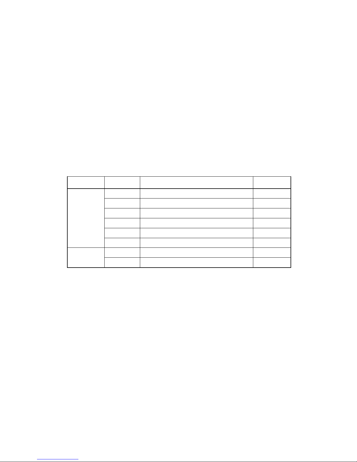
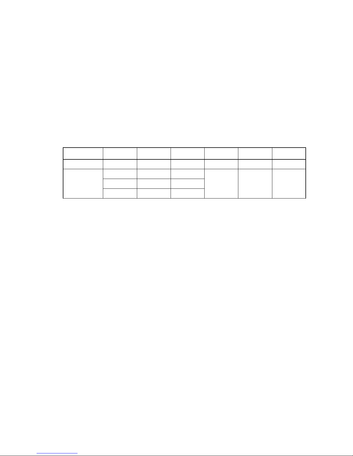
(4) The output on the secondary side is shown in Table 1.
(Refer to the power system diagram1-3 in Pages 1-3, 1-4 and 1-5.)
Table 1
1.1.2 Rectifying circuit
(1) The AC input voltage is rectified in the full wave mode with the diode bridge in D901.
(2) In the higher harmonic circuit of the section 1.1.4, the AC input current becomes the sine
wave form in the same phase with the AC input voltage waveform, but the interference is
given to other peripheral devices since the noise of the switching current appears on the
input side owing to the switching waveform. Therefore, L902 and C906 are inserted to
suppress the noise that is caused by the switching current.
1.1.3 Surge current suppression
(1) TH901 (thermistor) suppresses the rush current that flows when the power switch is turned
ON. Moreover, D933 is added to protect D902 from the rush current.
Power block
Main power
side
+215V
+80V
+15V
-15V
+12V
+7.5V
+5V
P-OFF+5V
H. deflection circuit, Video cut off circuit
Video circuit, DBF circuit, High voltage circuit
H/V deflection circuit, etc.
H/V deflection circuit, etc.
Video circuit, H. deflection circuit, etc.
Heater
MPU, etc.
Video circuit, etc.
Sub power
side
Output voltage
OFF
OFF
OFF
OFF
OFF
OFF
ON
OFF
When power save
Application
Page 7

1 - 2
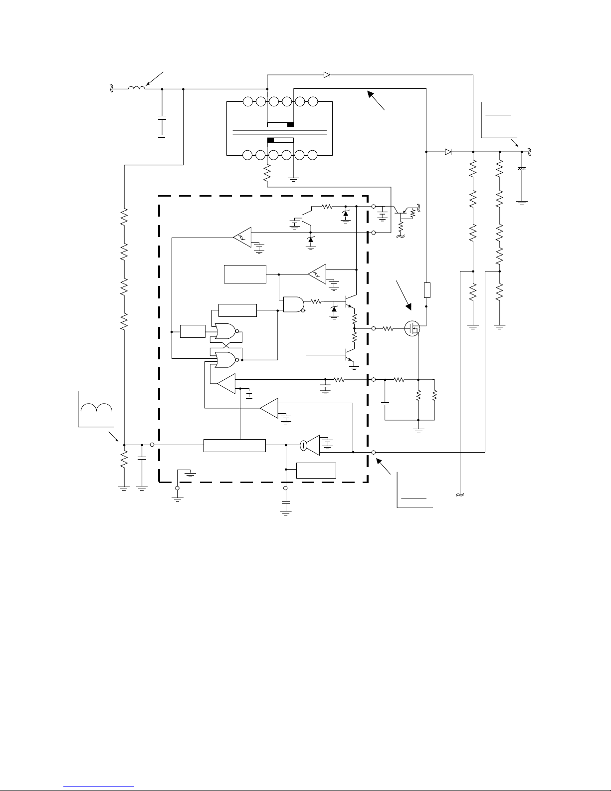
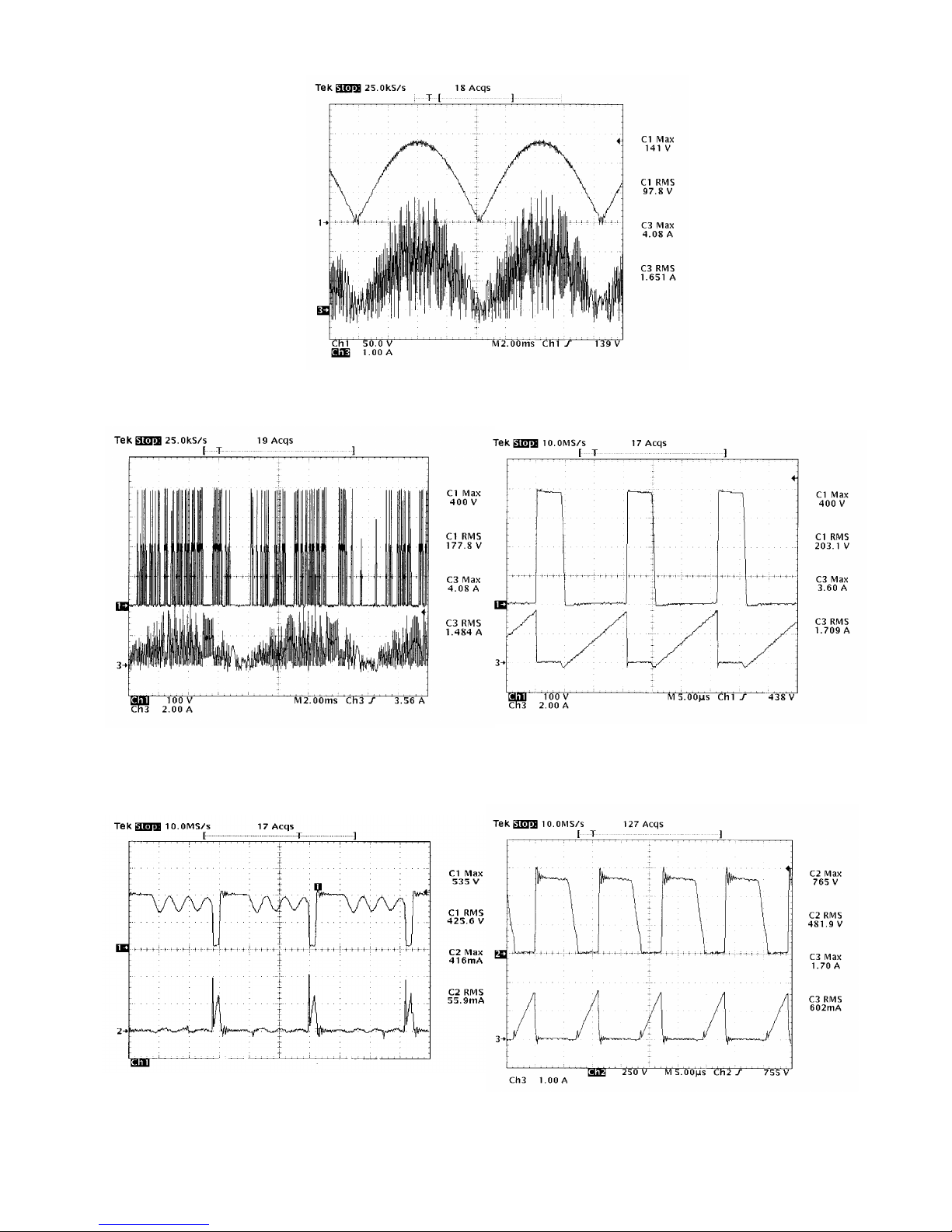
1.1.4 Higher harmonic circuit
(1) The pulsating waveform rectified in the full wave mode by D901 is switched throughout the full cycle
by the frequency of several tens kHz or more. Through this, the input current waveform becomes
an average of the switching currents of the partial cycles, thus becoming the sine waveform in the
macro. (See Fig.1)
(2) For the AC input voltage, the AC input current of the sine wave type in the same phase flows to
achieve the power circuit of improved power factor and reduced higher harmonic wave component.
(3) L903 is the choke coil, Q901 is MOS FET, D902 is the rectifying diode, C911 is the block capacitor,
and IC901 is the power factor improved controller. The power factor improved controller uses
MC33262P of Motorola. (See Fig. 2)
(4) After the sub power circuit operates, P-SUS signal becomes HI when +5V voltage is supplied to the
MPU. Then, Q902 is turned ON, the voltage of approx. +18V is supplied to pin8 (VCC terminal) of
IC901 through D929 from pin2 of T902, and the following operation is started.
(5) The pulsating voltage waveform rectified in the full wave mode by D901 is divided with R904, R905,
R906, R907 and R908 (100VAC : 1.1Vp-p and 240VAC: 2.9Vp-p), and is input to pin3 of IC901
(Multiplier input). Moreover, the output (+side of C911: 400VDC) of the higher harmonic circuit is
divided with R913, R914, R915, R916 and R917 (2.5VDC), and is input to pin1 of IC901 (error
amplifier input).
(6) The output of the error amplifier and the divided waveform of the pulsating voltage input to pin3 of
IC901 sets the threshold voltage of the current sense comparator to control the Q901 flowing
current from zero to the peak line of the AC input voltage in the sine wave pattern.
(7) When Q901 is turned ON, the drain current of Q901 flows to R910 and R937 to drop the voltage,
and the voltage generated by the voltage drop is input to pin4 (current sense input) of IC901. When
the voltage reaches the threshold voltage of the current sense comparator, Q901 is turned OFF.
(8) When Q901 is turned OFF, the accumulated energy of L903 starts to be supplied to the load
through D902.
(9) As the accumulated energy of L903 drops, the auxiliary coil voltage (pin8 of L903) also drops.
When it reaches the threshold voltage of *zero current detector, Q901 will be turned ON again.
* Pin 5 of IC901 is the zero current detection terminal to input the auxiliary coil voltage of pin10 of
L903. The zero current detector monitors that the auxiliary coil voltage drops beyond the thresh
old voltage. Thus, the accumulated energy of L903 is indirectly detected.
(10) The above operation is repeated to continue the oscillating operation. Thus, the DC voltage (L903,
Q901, D902 and C911 compose the voltage rise circuit.) is gained on the output, and the AC input
current of the sine wave in the same phase with the AC input voltage is gained on the input side.
0
Peak
IQ901
Averag
e
ID902
ON
MOSFET
Q901
OFF
Figure 1. L903 coil current
Page 8
1 - 3
PG
PG
PG PG
PG
Erroramplifier
10μA
Overvoltage
comparator
C908
PG
PG
R918
R904
C906
R905R906R907R908
C909
L905
R910
R937
C910
R911
R919R920
R913
C911
R914R915R916
R921
R917
D933
D902
IC901
L903
PG
L902
Waveform1
(RefertoP1-11.)
PG
PG
Quick
start
1.08Vref
TimerR
+
-
+
Vref
6 5 4 3 2 1
7 8 9 10 11 12
Delay
Multiplier
+
-
+
2.5VReference
voltagesource
+
-
+
13V/
8.0V
+
-
+
+
1.6V/
1.4V
RSlatch
Drive
output
UVLO
16V
10
20k
R912
R909
Q901
10pF
10
36V
1.2V
6.7V
Currentsense
comparator
Zerocurrentdetector
MC33262P
Waveform2,3
(RefertoP1-11.)
Figure.1
(RefertoP1-2.)
1
4
7
5
3
6 2
8
+
-
+
Vref
+
2.5V
Q902
400V
D
C
Figure 2. High harmonic waveform circuit
Page 9

1 - 4
1.1.5 Sub power circuit
(1) The sub power uses PRC control regulator STR-G6352 (IC903) produced by Sanken Electric. (See Fig.3)
(2) When the power switch is turned ON, the rectified and smoothened DC voltage (AC voltage
x ) is supplied to pin4 of IC903, through R950, R951 and R952. When pin4 reaches
approx. 17V, the built-in output FET is put into operation. (Since Q902 is OFF, IC902 and
IC 903 do not operate.)
(3) This also induces the voltage at pin2 of T902 and on the secondary side. These outputs
are respectively rectified, and are used as the power for control on the primary side and
the power for the MPU.
(4) IC903 monitors +5V and -15V output on the secondary side by IC922 (Shunt regulator),
and suppresses the voltage regulation by feeding back to pin 5 of IC903 via IC912
(Photocoupler).
(5) When the voltage on the secondary side starts, the MPU will be put into operation and the
P-SUS signal line will become HIGH.
(6) This information is transmitted to the primary side via IC913 to turn ON Q902.
When Q902 is turned ON, the power for control on the primary side will be supplied to
IC901 and IC902 to operate the higher harmonic circuit. Thus, the main power circuit will
be put into operation.
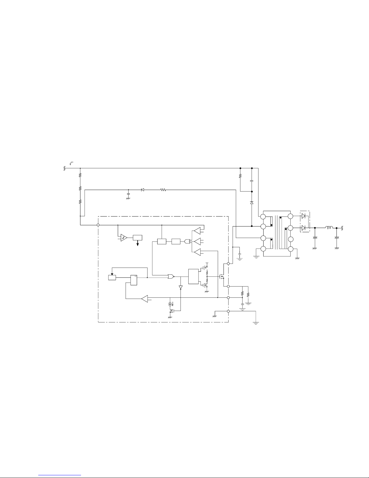
1.1.6 Main power circuit
(1) The main power circuit adopts the flyback type switching power of pseudo-reosonance
operation. This is composed of a Sanken brand hybrid IC STR-F6676 (IC902) that inte-
grates the power MOS-FET and control IC.
The circuit operation is described as follows. (See Fig. 4.)
(2) The timing at that the power MOS-FET is turned ON is consistent with the bottom point of
the voltage resonant waveform after the transformer (T901) discharges the energy to the
secondary side, that is, a half cycle of the resonant frequency determined by LP value
(primary coil inductor value) of T901, and C914 (resonant capacitor). This is called
pseudo-reosonance operation. The advantage of such an effect is that the switching loss
is reduced by turning it ON when the voltage between the drain sources of the power MOS-
FET becomes the lowest.
(3) Like the higher harmonic circuit, voltage of approx. +18V is supplied to the Vcc terminal
(Pin 4) of IC902 (STR-F6676) via D929 from pin2 of T902 when Q902 is turned ON by the
P-SUS signal from the MPU.
When the voltage of Pin 4 of IC902 reaches 16V, the control circuit will be put into opera-
tion to turn ON the integrated MOS-FET.
(4) When MOS-FET is turned ON, the capacitor C1 in IC will be charged to approx. 6.5V. On
the other hand, the drain current flows to R928, and the voltage generated by the voltage
drop is applied to pin1 (OCP/FB terminal) of IC902.
When the voltage of Pin 1 reaches approx. 0.73V, the comparator (Comp. 1) in IC will be
activated to turn OFF MOS-FET.
(5) The voltage between both ends of C1 drops to approx. 3.7V. the oscillator output will be
reversed again to turn ON MOS-FET.
The above is repeated to continue the oscillation operation.
(6) Here, IC902 monitors +215V of the output on the secondary side with IC921 (error ampli-
fier) and feeds back it to pin1 of IC902 via IC911 (photocoupler), thus suppressing the
voltage fluctuation of the primary side.
2
Page 10
1 - 5
Figure 3. IC903 (STR-G6352) block diagram and peripheral circuit
4
3
1
6
7
8
5
T902
R935
R950
(AC x 2 )V
R951
R952
Vin
4
D932
C931
C940
Icont
S Q
R
OSC
REG
Latch Delay
Drive
OVP
Vth=25.5V
Vth=0.73V
Vth=1.45V
Ta=160°C
TSD
Tri
REG1
PQM Latch
UVLO
Internal Bias
Toff=15µS
IC903 (STR-G6352)
Vin(on)=17.5V
Vin (off)=10V
OCP Comp.
D
GND
D971
L971
C972
C971
R931
R936C933
C939
D941
R939
++
+
-
+
-
+
-
+
-
+
-
2
1
2
5
3
Page 11
1 - 6
Figure 4. IC902 (STR-F6676) block diagram and peripheral circuit
C912
D904
R928
C916
C914
C917
Iconst
START
LATCH
DRIVE
REG.
T. S. D
Wavefo rm5
(Refer to P1-11)
5
4
3
4
3
2
9
7
T901
400V
D912
R927
2
1
-
+
Vth(1)
-
+
Vth(2)
Comp.1
Comp.2
Rconst -Rconst +
R2
R926
C1 R1
R3
R4
O.S.C
O.V.P
5
D908
R922
R923
R941
R925
IC902(STR-F6676)
Page 12
1 - 7
1.1.7 Degaussing circuit
(1) The automatic and manual degaussing circuit is provided.
The circuit prevents the picture from dropping its quality due to the magnetization on CRT,
and operates as follows.
(2) When powering ON, Q963 flows to activate RY901 by DG signal output by the MPU.
This will make the current flow through the demagnetizing coil for demagnetization. The
demagnetizing time is approximately 5 seconds.
Manual demagnetization becomes possible by selecting the demagnetizing menu on the
OSD picture.
1.1.8 Power management circuit
Turn ON the power management setting on the menu picture of OSD, and the energy saving
mode shown in Table 2 will be ready depending on whether the horizontal/vertical sync. signal
is present or not.
1.1.9 Protective circuit
(1) Overcurrent protective circuit (primary side)
IC902 is provided with an overcurrent protective circuit. The voltage drop generated by the
drain current that flows into R928 is input to Pin 1 (OCP/FB terminal) of IC902. When the
voltage reaches 0.73V, the overcurrent protective circuit will be activated.
(2) Overcurrent protective circuit (secondary side)
To protect the parts on the secondary side, the short-circuit detection circuit is provided on
the secondary side output (+215V, +80V, +/-15V, +7.5V), one for each. As an example of
+215V, the output line of +215V is monitored with R964, R965, D966 and Q961. If it drops
beyond approx. +140V for any reason, Q961 will be turned ON to transmit the information
to the MPU. Then, since the MPU sets P-SUS signal at LOW, Q902 will be turned OFF to
cut off the power to IC902 in order to stop IC902. (IC901 will be also stopped at the same
time.) The overcurrent protective circuit is designed to be activated when the output volt-
age drops approx. 30 to 40%.
(3) Overvoltage protective circuit
R918, R919, R920 and R921 are used to detect the overvoltage in the higher harmonic
circuit, and the tertiary coil (Pin 9) of T901 is used to detect the overvoltage of the voltage
on the secondary side. They are both connected to the overvoltage protective circuit
(Q904, Q905) on the primary side. If any overvoltage results for any reason, Q905 will be
turned ON to turn ON Q904. Then Q902 will be stopped. Since the power for IC901 and
IC902 is cut off as Q902 is stopped, the switching operation will be stopped.
OFF
ON
On
Off
On
Off
On
On
Off
Off
Active
Blank
Blank
Blank
Power Save Video
H-sync V-sync
LED indicator
140W
≦3W
Power
consumption
Recovery
time
―
5 sec.
Green
Amber
Page 13
1 - 8
+215V
+80V
+15V
-15V
P_OFF+5V
+5V
+7.5V(HEATER)
+215V
+80V
+15V
+12V
-15V
P_OFF+5V
+5V
+5V
+215V
+80V
+12V
+5V
P_OFF+5V
+7.5V(HEATER)
PWB-POWER
PWB-MAIN
PWB-VIDEO
+5V
-15V
+3.3V
PWB-DEFL-SUB
P_OFF+5V
-15V
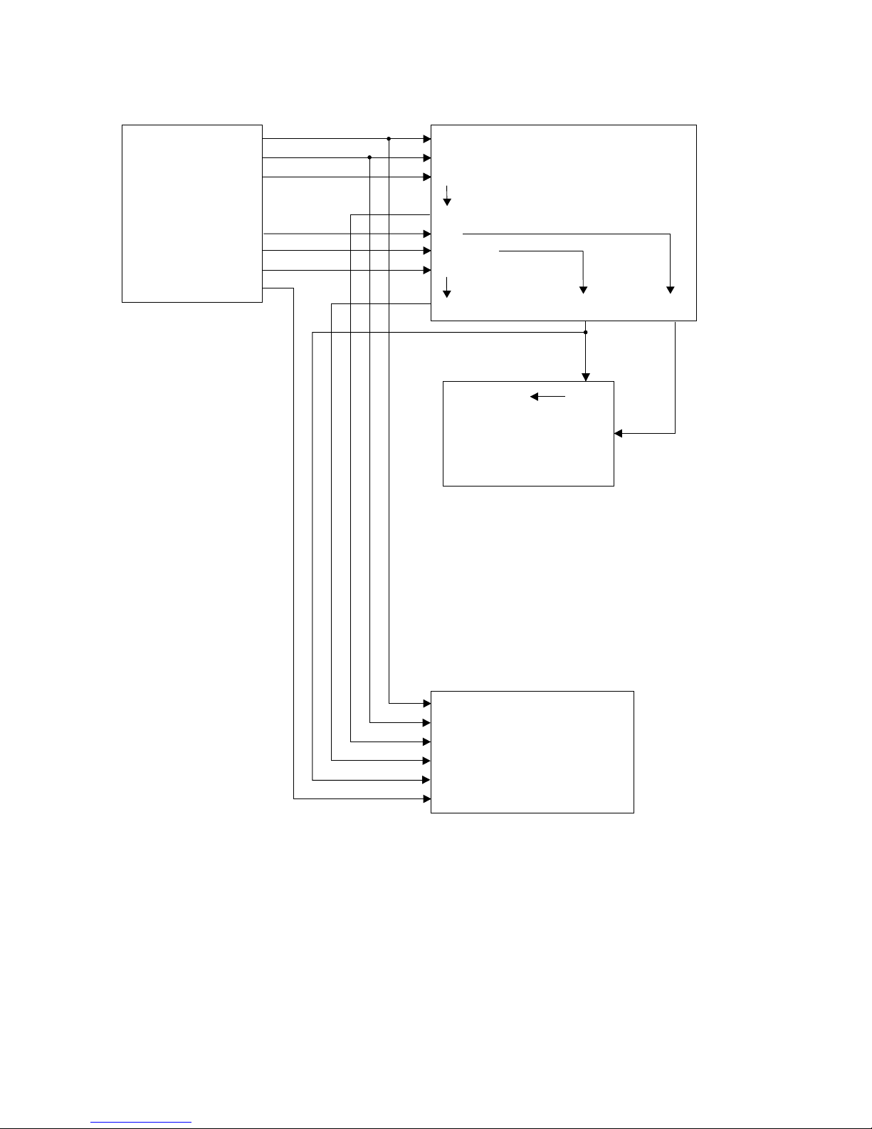
~ Power system diagram 1 ~
Page 14
1 - 9
PWB-MAIN
Horizotnal width/PCC
control circuit
+B
+15V
-15V
+12V
Horizontal drive circuit
-15V
MPU circuit
+5V
Vertical system circuit
+15V
-15V
DBF circuit
+80V
+12V
-15V
High voltage system circuit
+80V
+12V
Corner purity
H/V ROTATION
Drive circuit
+15V
-15V
P-OFF+5V
+80V
P-OFF+5V
-15V
+5V
Variable
circuit
(Chopper circuit)
+215V
+B
+15V
+12V
PWB-DEFL-SUB
Reg.
3.3VP_OFF+5V
P_OFF+5V -15V
~ Power system diagram 2 ~
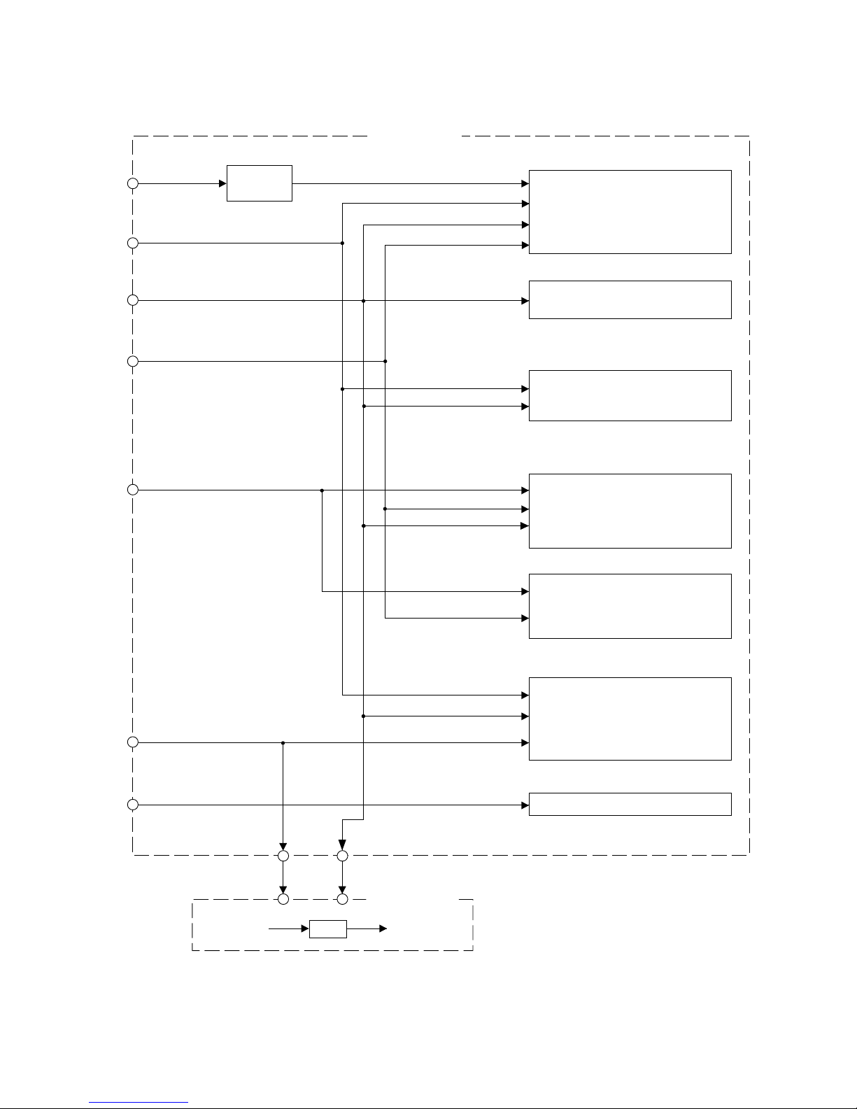
Page 15
1 - 10
PWB-VIDEO
Cut off circuit
+215V
+12V
Main amplifier circuit
+80V
+12V
OSD circuit
P-OFF+5V
Magnetic cancel circuit
+12V
Asset circuit
+5V
Preamplifier circuit
+12V
P-OFF+5V
+215V
+12V
P-OFF+5V
+80V
+5V
+7.5V(HEATER)
+7.5V(HEATER)
PWB-CRT
~ Power system diagram 3 ~
Page 16
1 - 11
Waveform 1. Top :AC input voltage
Bottom :AC input current
Waveform 2. Top :Q901 drain voltage
Bottom :Q901 drain current
Waveform 3. Top :Q901 drain voltage
Bottom :Q901 drain current
Waveform 4. Top :IC903 drain voltage
Bottom :IC903 drain current
Waveform 5. Top :IC902 drain voltage
Bottom :IC902 drain current
Page 17

1 - 12
1.2 Horizontal deflection block
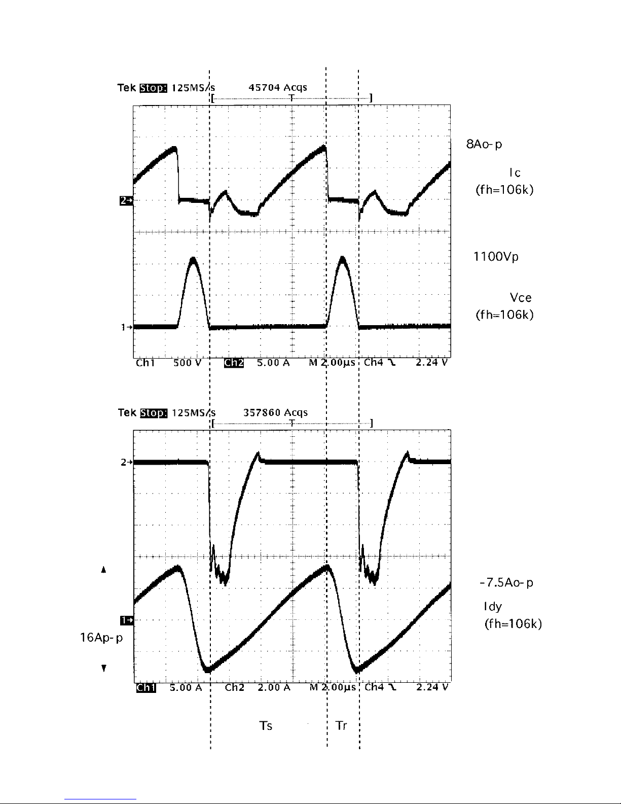
The operating principle of the horizontal deflection circuit is given below.
The Q502 operates as horizontal output, and the D503 as the dumper diode.
As shown in Fig. 5, the horizontal output transistor Q502 turns to ON/OFF by means of the drive pulse in
pin 25 of IC601 in substrate DEFL-SUB through the drive transformer T501, drive transistor Q501, or
Q560, Q561, Q562, etc.
The deflection current Idy during Q502 ON gets increased to the maximum level Ip according to the
equation shown below:
Idy = (Vcc/Ldy) x Ton
The maximum Ip is approximately 8A at full scan when fh = 106k.
Here;
Vcc: Output voltage of Q504
Ldy: Parallel value of the Lh value of DY (=62µH) and the horizontal output transformer
(=5mH)
TON: The ON time of Q502
When the drive pulse has negative polarity, Q502 turns OFF and Idy starts flowing to charge C506 until
the collector voltage reaches the maximum level Vcp.
Vcp = Vccx{1 + (π/2)x(Ts/Tr)}
With the maximum Vcp attained, the charges accumulated in C506 flow into DY as the discharge current.
This charge/discharge current is called retrace time, and is expressed by the equation given below.
Tr = π (Ldy•Cr) * Cr = C506 value
In the present model, the retrace time is set to approx. 1.8µs.
Ts is called trace time, and is expressed by the equation given below with the horizontal cycle as T.
T = Ts + Tr
With Vcp = 0, the dumper diode D503 turns ON and Idy gets decreased from –Ip to 0 ampere. Since
Q502 ON time and dumper diode ON time are set to overlap at 0 ampere point of Idy, the crossover
distortion is prevented from occurring at 0 ampere point of Idy.
The D503 causes the transient current to flow in the high-speed dumper diode.
The horizontal output transformer T502, connected in parallel to the deflection yoke, operates as a choke
coil. Figs. 6 and 7 show the image of circuit operation and the waveforms in actual machine.
Page 18

1 - 13
1.2.1 Distortion compensation waveform generating circuit
The deflection distortion compensation waveform for horizontal size system is output from pin
64 of IC601. This waveform is output from 1-bit DAC, with 3.3V pulse waveform with resolu-
tion 25MHz output at pin 64. This pulse waveform is leveled by the low-pass filters R632 and
C622 to obtain the vertical cycle compensation waveform, with the amplitude 1.0 to 1.2Vp-p
and connected to pin5 of IC5J1.
The compensation waveform circuit carries out horizontal size and trapezoid compensation,
side pin compensation, side pin top and bottom compensation, side pin S-shape compensation
and side pin W compensation. (Refer to Compensation Image Diagram in Fig. 22)
The deflection compensation waveform for horizontal phase system is output from pin 57 of
IC601. The pin 57 has 1-bit DAC output and outputs the 3.3V pulse waveform with 25MHz
resolution. This pulse waveform is then leveled by the low-pass filters R619, R614, C604 and
C601 to obtain the vertical cycle waveform, which is then electrically added to the horizontal
system PLL filter (pin 20 of IC601) to carry out the deflection distortion compensation of the
horizontal phase system. It carries out parallelogram distortion compensation and side pin
balance (top and bottom) correction. (Refer to the Compensation Image Diagram in Fig. 22.)
The control of horizontal screen width and the side PCC control are carried out by IC5J1, Q503
and Q504. First, the horizontal width signal and each distortion compensation signal im-
pressed in pin 5 of IC5J1 from pin 64 of IC601 are compared with the AFC pulse signal recti-
fied and fed back to pin 13 of IC5J1. The signals are further compared with the constant-
inclination type saw-tooth wave synchronized with the horizontal cycle created inside IC before
turning into the PWM signal of square wave. This PWM signal output from pin 9 of IC5J1
carries out the above control by driving the Q504 gate. Fig. 8 shows the block diagram of
IC5J1 and Fig. 9 the operation image waveforms.
IC5K1 connected to pin 8 of IC5J1 is a transistor with 2 circuits.
Pins 1 and 3 of IC5K1 are for the base, pin 2 is for GND and pins 4 and 5 are for the collector.
Pin 32 of IC101 connected to pin 3 makes pins 5 and 2 open/short by P-SUS signal.
When P-SUS signal is LOW, pin 8 of IC5J1 is led into GND from pin 5 of IC5K1, and make
SYNC input of IC5J1 LOW. As IC5J1 stops operation without SYNC input, Q504 turns OFF
and horizontal deflecting output stops.
Due to this process, destruction by wrong pulse is prevented when it exceeds in Q502.
The Q503 works as a ripple filter in 215V line and keeps the Q503 emitter voltage constant
even if there is a slight fluctuation in the collector voltage of Q503. The Q503 collector has
215V applied to it, with the emitter output being stable at 203V. This is mainly effective in
dynamic regulation.
The horizontal raster position is adjusted by using Q5A1, Q5A2, VR5A1 and T502. The refer-
ence voltage is obtained from the connecting point of Cs and is then input into pin 2 of T502.
When the emitter voltage in Q5A1 and Q5A2 has the DC level increased by adjusting VR5A1,
the current flows to DY side, causing the raster to move left. Reversely, when the DC level of
the emitter voltage is decreased, the current flows to Q5A2 side, causing the raster to move
right.
The Idy DC level is adjusted by varying the emitter voltage of Q5A1 and Q5A2 at the timing
No. 25 (120kHz/85Hz) using VR5A1, so that the raster position comes at the center of CRT.
The operation image is shown in Fig. 10.
This adjustment, however, is confined to the factory, and is not open to the users.
Page 19
1 - 14
Figure 5 Horizontal deflection circuit
Q503 Q504
T502
Q502
D503 C506
L540
LIN
IC501
Q540
Q510
215V
Page 20
1 - 15
Figure 6 Horizontal deflection circuit operation image
IC601outputwaveform
Q501Vce
Q502Ib
Q502Vbe
Q502Ic
Q502Vce
Dumperdiodescurrentwaveform
Idy
Page 21
1 - 16
Figure 7. Deflection circuit waveform while fh=106k
Q501
Q502
Q502
IC601 output waveform
(fh=106k)
Q501 Vce
(fh=106k)
Q502 Vbe
(fh=106k)
Q502 Ib
(fh=106k)
Page 22
1 - 17
Q502
Q502
Damper diode
Current waveform
(fh=106k)
Page 23
1 - 18
Q501
Q502
Q502
Deflection circuit waveform while fh=31.5k
3.3V
IC601 output waveform
(fh=31.5k)
Q501 Vce
(fh=31.5k)
Q502 Ib
(fh=31.5k)
-7Ao-p
Q502 Vbe
(fh=31.5k)
Page 24

1 - 19
Q502
Q502
Damper diode
Current waveform
Q502 Ic
Q502 Vce
Page 25
1 - 20
Vcc
Ref
IN
SAW
R
SAW
OUT
Buff
OUT
Buff
IN
Vreg GND
IN OUT Vcc
DTC HDIN
OUT
Err
SAWGen.
Err Power PWM
10 8911121314
543 7621
-
-
+
-
+
-
+
9.0V
Ref
HDIN
SAWOU
T
Erroramplifier
output
PWMOU
T
Figure 9. Operation image
Figure 8. IC5J1 block diagram
Page 26

1 - 21
0
0
0
Ip
Whenthepictureisthecenter
Whentherastermovestotheleft
Whentherastermovestotheright
0.8Ap-p
Figure 10 Horizontal position adjustment image
Page 27
1 - 22
1.2.2 Deflection current compensation circuit
As the picture becomes flatter, the arrival distance of the deflected electronic beam becomes
more different between the center and both ends of the picture. Therefore, there is a tendency
for the image to be contracted at the center of the picture and expanded at both ends of the
picture. Moreover, the left side of the picture is more expanded than the right side of the pic-
ture owing to the characteristics of the circuit. CS applies S type compensation to the deflec-
tion current with the resonant effect of the deflection yoke and contracts at both ends of the
horizontal axis. The linearity coil increases the inductance of the starting section of the deflec-
tion current with the supersaturated reactor, and works to contract the left side of the horizon-
tal axis.
As the frequency is lower, the capacity of CS is generally increased and the linearity coil with a
larger impedance value is used. In the practical circuit, seven CS capacitors are prepared, and
are combined as desired. The linearity coil changes inductance by letting the control current
corresponding to the horizontal frequency flow to the control coil.
(1) S type compensation with CS
CS is switched in seven steps by FET. IC501 element with six FETs included and Q510 are
used. On IC501, pins 2, 5, 7, 9, 11 and 13 are used as the gate, and pins 3, 6, 8, 10, 12
and 14 are used as the drain. Pins 1 and 15 are used as the ground, and each source are
grounded to the earth. The binary value signal of HIGH (5V) or LOW (0V) is input to each
gate by IC102. In case of HIGH, FET is turned ON. In case of LOW, FET is turned OFF.
The correspondence to the signals from the capacitor and IC102 are as follows.
(2) Compensation with linearity coil
The linearity coil compensates the left expansion of raster by changing the inductance
value through the current value flow in order to keep the horizontal linearity to appropriate
level. In the actual circuit, L540 stands for the linearity coil.
The newly adopted linearity coil is provided with a control winding capable of controlling the current
characteristics of the inductance value. The control voltage (DC) corresponding to each horizontal
frequency is supplied from pin 2 of IC101 to pass the control current to the control winding through
IC103 and Q540. This controls the current characteristics of the inductance value, and eventually
keeps the horizontal linearity to appropriate level. An image of characteristic of linearity coil is as
fugure 11.
Table 3
The column of G and D is Pin No.
Capacitor
Signal
FET1
FET2
FET3
FET4
FET5
FET6
FET7
(Q510)
2
5
7
9
11
13
3
6
8
10
12
14
C523
C524
C525
C526
C527
C528
C529
CS2
CS1
CS5
CS6
CS3
CS4
CS7
DG
Page 28
1 - 23
As shown in the Table 4 below, CS is switched on the horizontal frequency bands. 1/0 in the
table express the signals from IC101 with 1 for HIGH and 0 for LOW. Here, the column of the
frequency expresses the lower limit value.
20.00
15.00
10.00
5.00
Inductance(mH)
-11 -6
-1 4 9
Deflectioncurrent(A)
0.00
ControlcurrentOA
Controlcurrent
200mA
Figure 11 Characteristic of variable lineality
Fh
(kHz)
CS7
0.024
CS6
0.056
CS5
0.15
CS4
0.24
CS3
0.47
CS2
0.82
CS1
1.3
com
0.173
total
31
34
36.5
39
45
47.5
49
52
55
59
61
63
66
70
73
76
78.5
81.5
83
86.5
89
92
94
97
104
108
111
114
116
125
31k/60
46k/75
60k/75
68k/85
80k/75
91k/85
93k/75
106k/85
112k/75
120k/85
CS7
0.024
1
0
1
0
0
1
0
1
0
1
CS6
0.056
1
1
0
1
0
1
0
1
1
0
CS5
0.15
1
0
0
1
1
1
1
0
0
0
CS4
0.24
1
0
1
1
1
0
0
0
0
0
CS3
0.47
1
1
1
0
0
0
0
0
0
0
CS2
0.82
1
1
0
0
0
0
0
0
0
0
CS1
1.3
1
0
0
0
0
0
0
0
0
0
com
cs
0.173
0.173
0.173
0.173
0.173
0.173
0.173
0.173
0.173
0.173
total
Cap.
3.233
1.519
0.907
0.619
0.563
0.403
0.323
0.253
0.229
0.197
timing
1
0
0
0
0
0
1
1
0
1
0
0
1
1
0
0
1
0
0
0
0
0
0
0
1
1
0
0
1
0
1
0
0
0
1
1
1
1
0
0
0
0
1
1
1
0
1
1
1
1
1
0
0
0
1
1
1
1
0
0
1
0
1
1
0
0
1
1
1
0
0
0
1
1
1
1
0
0
0
1
1
1
1
1
0
0
0
0
0
0
1
1
0
1
0
0
1
1
1
1
1
1
1
1
1
1
1
1
1
0
0
0
0
0
0
0
0
0
0
0
1
0
0
1
1
1
1
1
1
1
1
1
0
0
0
0
0
0
0
0
0
0
0
0
0
0
0
0
0
0
1
1
1
1
1
1
0
0
0
0
0
0
0
0
0
0
0
0
0
0
0
0
0
0
0
0
0
0
0
0
1
1
1
0
0
0
0
0
0
0
0
0
0
0
0
0
0
0
0
0
0
0
0
0
0
0
0
0
0
0
0.173
0.173
0.173
0.173
0.173
0.173
0.173
0.173
0.173
0.173
0.173
0.173
0.173
0.173
0.173
0.173
0.173
0.173
0.173
0.173
0.173
0.173
0.173
0.173
0.173
0.173
0.173
0.173
0.173
0.173
3.233
2.533
2.443
1.853
1.519
1.519
1.113
1.113
1.033
0.907
0.883
0.883
0.643
0.643
0.619
0.563
0.493
0.469
0.469
0.379
0.379
0.323
0.323
0.323
0.253
0.253
0.229
0.229
0.197
0.173
User Timing
Preset Timing
1: ON 0: OFF
Table 4
Page 29
1 - 24
The waveform of the deflection current is compensated from Fig. (a) to Fig. (b) through the
above. The starting section of the current is smoothened, and the linear section becomes the
S type.
1.3 Vertical output block
The vertical deflection circuit controls the vertical width and vertical position with IC601 on the
DEFL_SUB substract, and IC603 controls the linearity. Moreover, the signal output from IC603
is input to the vertical deflection output IC401.
Figure(a)
Figure(b)
Figure 12 IC401(LA7841L) Pin connection & Function Block diagram
-15V
Ver.OUTPUT
OUTPUT
STAGEVCC
INVERTING
INPUT
PUMPUPOUT
NONINV.INPUT
+15V
1
234567
AMP
−
+
PUMP
UP
THERMAL
PROTECTION
Page 30

1 - 25
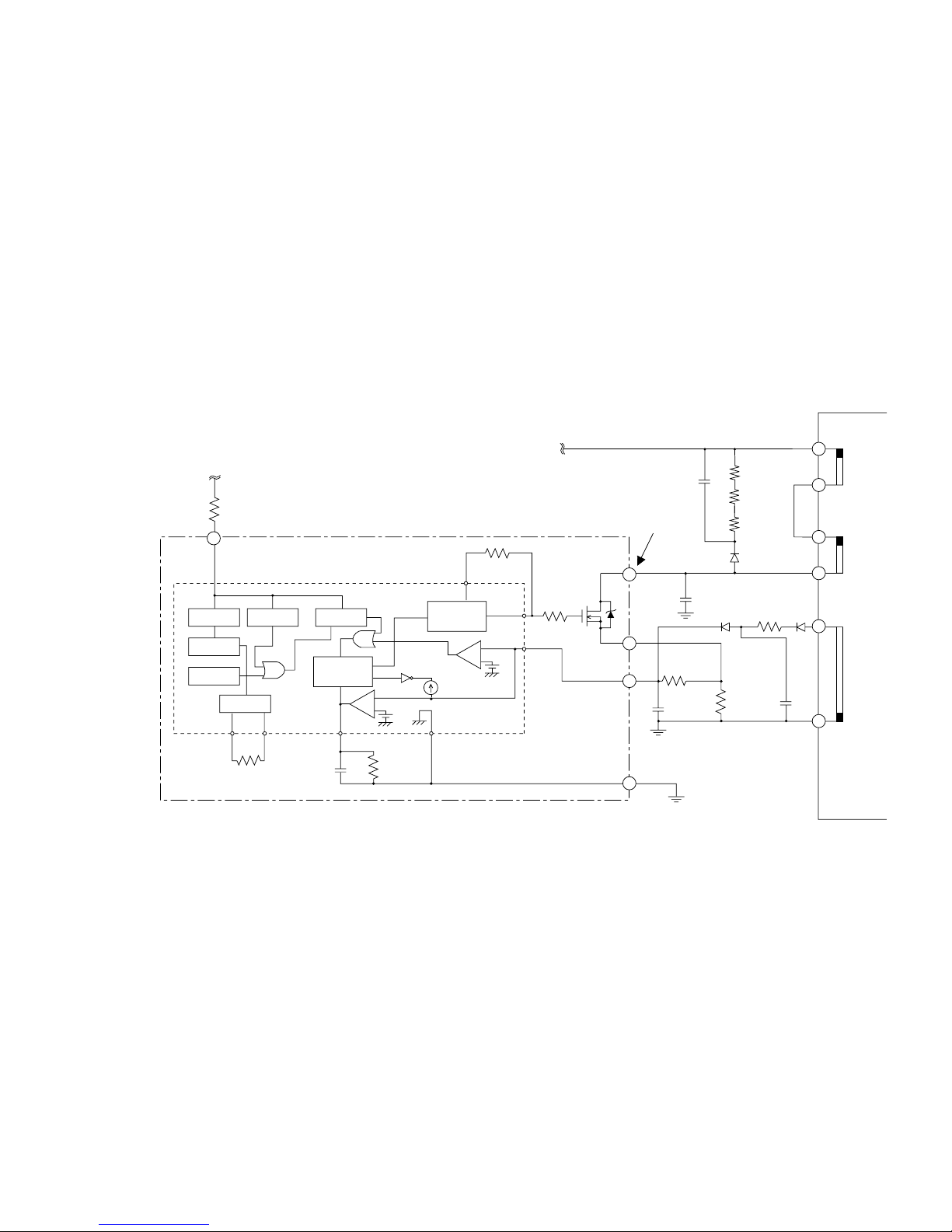
1.4 High voltage block
The high voltage circuit is composed of the high-voltage regulator IC701, MOS-FET Q701
flyback transformer (FBT) T701, operation amplifier IC702 and their peripheral circuits.
1.4.1 High voltage control circuit
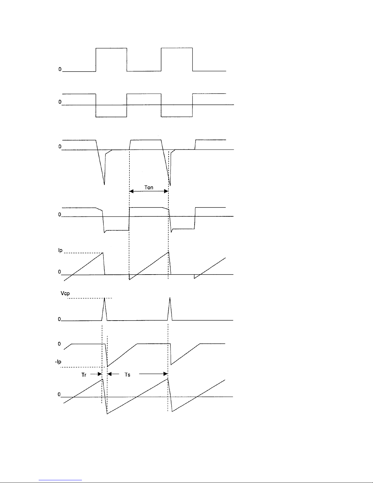
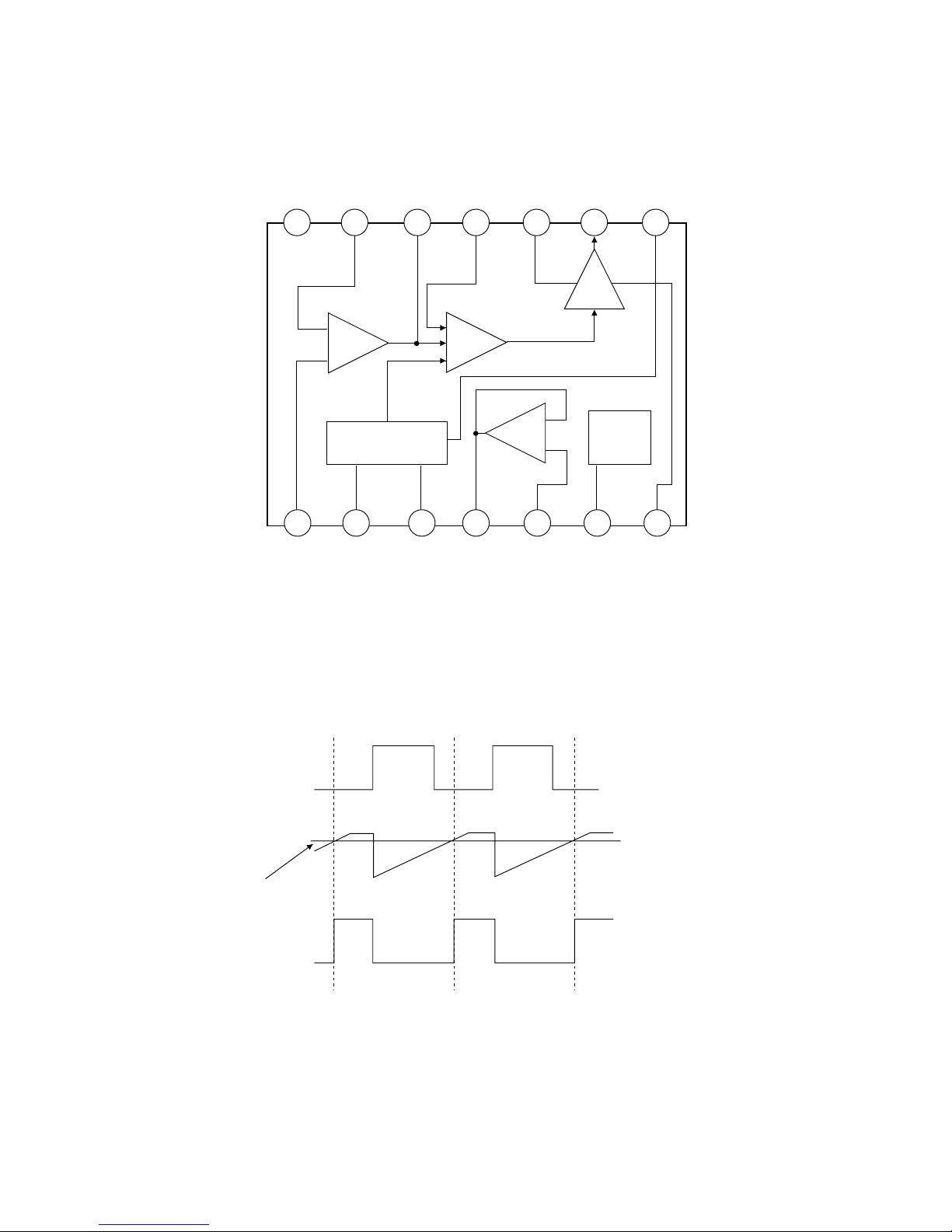
The IC701 is an IC for high voltage control, with the block diagram given in Fig.13. The OFF trigger PWM
control system is adopted to carry out high voltage control. The built-in VCO circuit gets synchronized
when the horizontal synchronous signal (hereafter SYNC signal) is input from Pin 3 of IC701 (horizontal
synchronous input terminal). Thus, the MOS-FET Q701 is controlled to turn OFF with the timing of the
SYNC signal changing over to HI, and is called OFF trigger system.
Further, the DC voltage, output after the feedback signal (IC701 Pin 11) from FBT T701 is compared with the
high-voltage set voltage (IC701 Pin 12) from IC101 in the internal error amplifier, is compared with the sawtooth-waveform of VCO to control the pulse output DUTY so as to keep the high voltage constant
(PWM control).
The timing chart for OFF trigger PWM control system is given in Fig.14. Set the high voltage by selecting
[HVADJ] in OSD and manipulating +/- button (Standard value: 27.0kV).
1.4.2 Protective function circuit
(1) Start and stop of high-voltage regulator IC701
The IC701 starts operation when Vcc voltage (power voltage applied to Pin 2 and Pin 10) attains the
level of 8.4 Vtyp, and the operation stops when the Vcc voltage is less than 7.4 Vtyp.
(2) IC701 overcurrent protection (OCP) function
It detects the peak value of the drain current in MOS-FET Q701 per pulse and stops DRIVE when the
voltage in Pin 6 of IC701 detecting the end-to-end voltage of the source resistors (R706 and R707),
exceeds 1.0 Vtyp until the next SYNC signal is input.
(3) IC701 overload protection (OLP) function
This function brings the system to the latch stop when OCP gets continuously activated due to
continuous overload.
It forms time constant using C716. With OCP activated and C716 charged and the voltage in Pin 8 of
IC701 exceeding 2.5 Vtyp, IC701 gets set to Latch mode, bringing the control operation to stop. This
status does not get released (reset) until the Vcc voltage (power voltage applied to Pin 2 and Pin 10)
in IC701 is less than 7.4 Vtyp.
(4) Over-voltage protection function for anode voltage (X-ray protector)
A voltage proportional to the high voltage is generated in Pin 6 of T701 due to the winding ratio
between secondary and tertiary winding inside FBT T701. This voltage is then rectified by D707 and
C708 and is further divided by R708 and R709 before being input in Pin 17 of microcomputer IC101
for comparison with the X-Pro set value. In case the voltage exceeds the set value, the output in Pin
33 of microcomputer IC101 gets fixed to LOW (P-OFF mode). With the mode set to P-OFF, the
application of voltage Vcc to IC701 stops, causing the IC701 operation to stop. The status continues
until the power SW is turned OFF. The overvoltage protection function is set to operate when the
high voltage level reaches 30kV (with the beam current is approx. 1mA).
(5) Overcurrent protection function for beam current (beam protector)
The beam current is supplied from +12V power source through R722. Since the end-to-end voltage of
R722 varies according to the beam current, the voltage drop due to R722 becomes large if the beam
current increases. The voltage in Pin 9 of FBT T701 (the voltage obtained by subtracting the voltage
drop due to beam current from the +12V power voltage) undergoes resistance division by R723 and
R724, and is then input into Pin 6 of operation amplifier IC702 for comparison with Pin 5 of IC702
(reference voltage). The voltage is then output (Pin 7 of IC702) and is input into Pin 16 of microcomputer IC101. The voltage in Pin 7 of IC702 (output terminal) is output linearly due to the fluctuation in
beam current. However, if the terminal voltage in Pin 16 of IC101 exceeds Beam-Pro setting value (ABL
data +70 : Max. 254), the output of Pin 33 of IC101 gets fixed to LOW (P-OFF mode). With the mode
set to P-OFF, the application of Vcc voltage to IC701 stops, causing the IC701 operation to stop. This
status continues until the power switch is turned OFF. The overcurrent protection function is set to
operate when the beam current reaches the level of approximately 1300µA.
Page 31

1 - 26
Figure 14. OFF trigger PWM control system timing chart
Figure 13. High voltage regulator IC701 block diagram
10
11
1214
15
16
5
4
3
2
1
9
−
+
13
SYNC-IN
DUTY
ADJUSTMENT
VCO
Isdetection
input
SYNC
IN
Vcc2
12V
PWM
output
GND2
RAMP
GEN.
PROTECT
6
7
GND1
Vcc2
12V
SW COMP
Condenser
connection
forDTC
HV
ADJ
FEED
BACK X-RAY
Vcc1
12VGND2
8
−
−
+
DTC
Condenser
connection
forDUTY
adjustment
Condenser
connection
forIS
detection
Resistance
connection
forDUTY
adjustment
SYNC. signal
input (3pin)
Vds wave form
Threshold voltage for
MAX DUTY
adjustment (5pin)
Saw-tooth wave for
MAX DUTY
adjustment (4pin)
Err AMP output
voltage
(13pin)
RAMP wave form
PWM output
(1pin)
Id wave form
Page 32

1 - 27
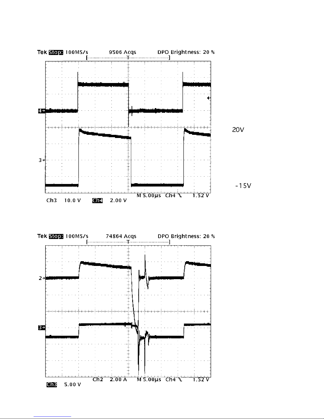
1.4.3 DBF (Dynamic Beam Focus) circuit
Since the display is flattened, the focus becomes unequal between the center and circumfer-
ence of the picture. To compensate for it, it is necessary to superimpose the parabola voltage
of 370Vp-p in the horizontal cycle with the static focus (with the horizontal width is 396mm) and
the parabola voltage of 145Vp-p in the vertical cycle. The slight voltage that is generated from
the parabola voltage generating circuit is amplified and reversed to generate the high voltage
in order to keep the focus equal. This circuit is called DBF circuit.
As shown in Fig. (16), the circuit is composed of the parabola voltage generating circuit IC601,
amplifier section IC6A1 in the front step, Q7A1 to Q7B5 of amplifier section in the rear step,
T7A1, and so on.
Videoperiod
Figure15
IncaseofthehorizontalDBF:370Vp-p
IncaseoftheverticalDBF :145Vp-p
Approx. 350V
Vertical DBF Horizontal DBF
90V
Q7B1
Q7B2
Q7B4
Q7B5
R7A5
R7B7
R7B9
IC6A1
IC601
DEFL-
PROCESSOR
IC
OP-AMP
Q7A1
R7A5
R7A4
R7A6
T7A1
R7A3
To FBT
Q7B3
Figure 16
Page 33

1 - 28
After the horizontal and vertical DBF
voltage are separately generated, they are
amplified and are finally composed.
<Horizontal section>
The voltage (approx. 0.5Vp-p) of the pa-
rabola waveform shown in Fig. (a) is output
from the deflection processor IC (IC601),
and is amplified approx. 10 times by OP-
AMP (IC6A2). Thereafter, it is amplified to
50 to 60Vp-p by the transistor (Q7B1 and
Q7B2). The amplification ratio is deter-
mined by the ratio between the resistors
R7B6 and R7B7, being approx. 10 times.
Moreover, the waveform is reversed as
shown in Fig. (b) at this time. Then, it is
amplified to approx. 500Vp-p by DBF
transformer (T7A1). The coil ratio between
the primary and secondary coils of the DBF
transformer is 1: 10, being the amplifica-
tion ratio of approx. 10 times.
<Vertical section>
The voltage (approx. 1.0Vp-p) of the pa-
rabola waveform shown in Fig. (a) is output
from the deflection processor IC (IC601),
and is amplified approx. 4 times by OP-
AMP (IC6A2). Thereafter, it is amplified to
approx. 160Vp-p by the transistor (Q7A1).
The amplification ratio this time is deter-
mined by the ratio between R7A3 and
R7A4, being approx. 40 times.
The horizontal and vertical DBF voltages
amplified and reversed are composed by
applying vertically synchronous modulation
to the output on the secondary side as
shown in Fig. (c). The composed voltage
is input to Pin 12 of the flyback transformer
(T701).
Figure(a)
Figure(b)
Figure(c)
VerticalDBF
HorizontalDBF
Horizontalperiod
Verticalperiod
Page 34

1 - 29
1.5 CRT compensation block
1.5.1 Rotation circuit
The rotation circuit is a circuit to compensate the picture inclination caused by the earth mag-
netism by letting DC current flow to the rotation coil wound on the front side of DY for adjust-
ment. It is controlled to 0 to 5V with the reference of 2.5V by IC103 pin 3 (PWM_DAC), and
DC current of +/-90mA (max) is made to flow to the rotation coil by IC804 pin 2.
This correction circuit has two functions; (1) User adjustment (OSD display) and (2) Southern/
Northern horizontal magnetic field rotation cancellation, as follows.
(1) User adjustment (OSD display)
User provides DC current to the rotation coil according to the value displayed on OSD.
(2) Southern/Northern horizontal magnetic field rotation cancellation
Southern/Northern horizontal magnetic field rotation cancellation is to automatically adjust
the variation of raster rotation by earth magnetism.
Detection voltage and direction of the southern/northern horizontal magnetic field (pin 2 of
IC214) is detected by IC214 (Earth magnetism sensor unit), and pin 18 of IC101
(CPU_ADC) reads the detected voltage and provides DC current to the rotation coil ac-
cording to the prescribed control program.
1.5.2 Corner purity circuit
The corner purity circuit is a circuit to compensate for the color shade and color deviation of
the picture corner. On the rear side of CRT, it is adjusted by DC current flowing to the corner
purity coils installed in the four corners on the display surface.
The compensation circuit is composed of the following four functions of (1) User adjustment
(OSD display), (2) Aging variation compensation, (3) High/low temperature drift compensation
and (4) Southern / Northern horizontal magnetic field landing cancellation.
(1) User adjustment (OSD display)
The user causes DC current of +/-60mA (max.) to flow to the purity coil of each corner
according to the value displayed on OSD.
(2) Aging variation compensation
As the electronic beam collides with the aperture grille, it is thermally expanded and con-
tracted. The thermal expansion/contraction is varied according to the elapse of the power
ON/OFF time of the monitor. The color shade and deviation of the picture corner thus
generated are automatically adjusted.
The voltage of the beam current supply pin (T701 pin 9) is detected with R723/R724, and
the voltage that detects the time elapse of the power ON/OFF of the monitor is read from
the CR charge (integration) circuit composed of C723 and R736 and CR discharge (inte-
gration) circuit, composed of C723 and R737 through IC702 (buffer amplifier) by IC101 pin
15 (CPU_ADC), and the DC current of +/-17mA(max) flows to the purity coil on each corner
according to the specified control program.
(3) High/low temperature drift compensation
The front panel (glass) is thermally expanded and contracted as the temperature varies in
the installation environments of the monitor. The color shade and deviation of the picture
corner are automatically adjusted. The voltage that detects the temperature variation of
the installation environments of the monitor is read from the environment temperature
detection circuit composed of TH101 (thermistor) arranged near the front panel (glass) by
IC101 pin 14 (CPU_ADC), and DC current of +/-13mA (max) is made to flow to the purity
coil on each corner according to the specified control program.
Page 35

1 - 30
(4) North-south horizontal field landing cancel
The north-south horizontal field landing cancel carries out automatic adjustment of color shading and
color shift occurring appeared in the opposite derection at the top and bottom end of the monitor
display surface in the horizontal direction.
The detecting voltage and direction of the north-south horizontal field (IC214 pin 2) are detected by
IC214 (geomagnetic sensor unit), the detecting voltage is read by IC101 pin 18 (CPU_ADC), and the
direct current of ±20mA (max) flows in each corner purity coil according to the specified control
program. (Four-corner interlock control)
• The left upper corner on the display surface is controlled with 0 to 5V of 2.5V reference
by IC101 pin 6 (PWM-DAC), and the DC current of the above value is made to flow to
the purity coil on the left upper corner by IC803 pin 2.
• The right upper corner on the display surface is controlled with 0 to 5V of 2.5V refer
ence by IC101 pin 7 (PWM-DAC), and the DC current of the above value is made to
flow to the purity coil on the right upper corner by IC803 pin 8.
• The left lower corner on the display surface is controlled with 0 to 5V of 2.5V reference
by IC101 pin 8 (PWM-DAC), and the DC current of the above value is made to flow to
the purity coil on the left lower corner by IC801 pin 2.
• The right lower corner on the display surface is controlled with 0 to 5V of 2.5V reference
by IC101 pin 9 (PWM-DAC), and the DC current of the above value is made to flow to
the purity coil on the right lower corner by IC801 pin 8.
1.5.3 Earth magnetism cancel circuit
The earth magnetism cancel circuit has a south-north horizontal magnetic field canceling
function and a vertical magnetic field canceling function.
IC214 (earth magnetism sensor unit) detects the voltage and direction of the south-north hori-
zontal magnetic field (IC214 pin 2) and the vertical magnetic field (IC214 pin1), and IC101 pins
18 and 19 (CPU_ADC) reads the detected voltage to automatically control the following cancel-
ing function according to the specified control program.
Here, the output voltage of IC214 (earth magnetism sensor unit) operates as follows.
• South-north horizontal magnetic field (IC214 pin 2): 0.8V(-0.04mT) to 2.5V(+/-0.00mT) to
4.2V(+0.04mT)
• Vertical magnetic field (IC214 pin 1) : 3.3V (-0.04mT) to 2.5V (+/-0.00mT) to 0.5V (+0.10mT)
<South-north horizontal magnetic field canceling function>
(a) Horizontal magnetic field landing cancel
The horizontal magnetic field landing cancel circuit is a circuit to compensate for the color
shade and deviation that appear in the horizontal direction that becomes the opposite
direction at the upper and lower ends on the monitor display surface, and the automatic
adjustment is done by DC current flowing to the corner purity coil that is wound around the
display surface. (synchronized control for four corners)
(Refer to 1.5.2 (4) for detail.)
(b) Horizontal magnetic filed convergence cancel
The horizontal magnetic field convergence cancel circuit is the circuit to compensate for
the misconvergence that results after the vertical convergence of RED and BLUE in the
whole display area of the monitor deteriorates, and it is automatically adjusted by DC
current flowing to the 4V convergence compensation coil mounted on DY. It is controlled
with the DC component (V-CONVERGENCE) by IC601 pin 60 (4V_SC), and DC current of
+/-30mA (max) is flowen to the 4V convergence compensation coil by IC8A1 pin 6 (Power
Opamp).
Page 36

1 - 31
<Vertical magnetic field canceling function>
The vertical magnetic field landing cancel circuit is the circuit to compensate for the color
shade and deviation that reaches its maximum at the center in the horizontal axis direction
and its minimum at the upper and lower ends on the monitor display surface, and the
adjustment is done by DC current according to the value displayed on OSD flowing to the
speed modulating coil installed in the neck part of CRT.
It is controlled with 0 to 5V of 2.5V reference by IC101 pin 4 (PWM-DAC), and DC current
of +/-140mA (max) is made to flow to the speed modulating coil by IC804 pin 8.
1.5.4 Digital dynamic convergence clear (DDCC) circuit
In the digital dynamic convergence clear (hereafter called DDCC) circuit, the convergence
compensating current waveform is produced and amplified, and the convergence is compen-
sated by the compensation current flowing to the sub yoke that is installed as the rear unit of
the deflection yoke.
Though the principle of the convergence compensation with the sub yoke is same as the CP
ring, the CP ring is used for the static variation with the parallel movement in the whole picture
in the uniform magnetic field with the permanent magnet but the sub yoke is used for dynamic
variation that compensates a desired position on the picture by controlling the current wave-
form that flows to the coil of the electric magnet.
(See Fig. 18)
(1) Production of compensation current waveform
There are 30 kinds of compensation elements, and they are programmed in
IC601(CP267P151=uPD61882BGC) one by one by using the functions. The amplitude of
the current is controlled by inputting the compensation coefficient into the function.
Red:
Blue:
b11T
b11B
YHTT&YHTB
YHJT&YHJB
b11B
b11T
b12T
b12B
b12T
b12B
V
V
YHTT=b11T・y^
2
YHTB=b11B・y^2
YHJT=b12T・y
YHJB=b12B・y
YHT=b11T・y^2+b11B・y^
2
YHJ=b12T・y+b12B・y
↓
4HSC=all・(YHT+YHJ)
Figure 17 DDCC compensation image
Page 37

1 - 32
Examples of the functions and current waveform/compensation operation of YH(YHTT,
YHTB, YHJT, YHJB) are shown as follows.
In the above formulas, b11T, b11B, b12T and b12B express the compensation coefficients,
and y and y^2 express the primary and secondary functions of the vertical frequencies.
The other parts except the compensation coefficients are programmed, and desired ampli-
tudes (= compensation amount) are gained by varying the coefficients.
YHTT and YHTB compensate the upper and lower parts of the picture of the characteristic
components of their DYs to compensate the upper and lower parts of the picture of the
axis deviation component. The component gained by adding YHT and YHJ is multiplied by
the offset compensation coefficient a11. The resultant component is regarded as 4H_SC,
and is output from IC601 (CP267P151=uPD61882BGC) pin 61.
(2) Waveform, and operation on the picture
The case in which the currents flow through 4H coils of the sub yoke is explained. Re-
garding YHT (secondary function in the vertical frequency), in case of Fig 17 as an ex-
ample, the current is large in the same direction at the start (upper end of the picture) and
the end (lower end of the picture) of the vertical frequency, and is zeroed on the X axis of
the picture. Therefore, the magnetic field that is proportional to it is generated, and RED
and BLUE vary in the same direction only at the upper and lower ends of the picture. As
aforementioned, YHT can be independently controlled at the upper part (b11T.y^2) and
lower part (b11B.y^2).
Moreover, regarding YHJ (Primary function in the vertical frequency), if the flowing direc-
tion of the current is opposite at the start (upper end of the picture) and the end (lower end
of the picture) of the vertical frequency as an example, RED and BLUE vary in the oppo-
site direction only at the upper and lower ends of the picture. Compensation in the vertical
direction can be done by making the current flow to the 4V coil.
Fig.19(a) and (b) shows the image of each adjustment item of the DDCC adjustment.
(3) Adjustment method
Before the adjustment with the compensation circuit, it is necessary that they are properly
adjusted at the center (H-STATIC and V-STATIC), on the X axis (XH slider, B-Bow 4P, XV
differential coil) and on the Y axis (YH volume, YV volume).
Though DC current is superimposed on the sub yoke, H-STATIC and V-STATIC are
pushed to the greatest possible extent by the adjustment with CP ring in order to reduce
the stress of the driver IC8A1 (STK391-110).
Moreover, since 4H and 4V coils alone are installed on the chassis, it is first necessary
that the convergence of RED, BLUE and GREEN (6H, 6V) satisfy the specifications for the
performance of ITC(CRT&DY).
As the adjustment procedure, the adjustment values of 30 elements are not respectively
zeroed but they are adjusted to nearest to zero with a total balance in good order.
In other words, the balance (compromise) adjustment with each adjustment item is applied.
The correspondence of the names of DDCC adjustment mode to the coefficients of all 30
elements is shown below.
Page 38

1 - 33
(4) Block diagram
Fig. 20 shows the block diagram of the DDCC circuit.
The components 4H_DC(pin 6), 4H_SC(pin 61), 4V_DC(pin 8) and 4V_SC(pin 60) supplied
from IC601(CP267P151=uPD61882BGC) to 4H-Coil and 4V-Coil are output, the dynamic
component (4H_DC, 4V_DC) is amplified with IC6A1(TL084), and the static component
(4H_SC, 4V_SC) is amplified with IC6A2(KIA4558).
DCC(pin 7) output from IC601 (CP267P151=uPD61882BGC) and DEFL_+3.3V(pin 3)
output from IC602 (TA48M033F) are respectively the reference voltage of Op-
Amp(IC6A1:TL084) that amplifies the above dynamic component (4H_DC, 4V_DC) and the
reference voltage of Op-Amp(IC6A2:KIA4558) that amplifies the static component (4H_SC,
4V_SC).
On each of 4H and 4V, the waveform added with the dynamic component and static com-
ponent is input to IC8A1 pin 3 and pin 4 (STK391-110) allow the specified current to flow to
each convergence compensation coil.
Table 5
b11T
b21L
b31TL
b41TL
c11T
c21L
c31TL
c41TL
YHTT
XHL
S3HTL
PQHTL
YVTT
XVL
S3VTL
PQVTL
y^2
x^2
x^2・-(y^3+y^4+y^5+y^6)
x^2・y^4
y^2
x^2
x^2・-(y^3+y^4+y^5+y^6)
x^2・y^4
b11B
b21R
b31TR
b41TR
c11B
c21R
c31TR
c41TR
YHTB
XHR
S3HTR
PQHTR
YVTB
XVR
S3VTR
PQVTR
y^2
x^2
x^2・-(-y^3+y^4+y^5+y^6)
x^2・y^4
y^2
x^2
x^2・-(-y^3+y^4+y^5+y^6)
x^2・y^4
b12T
b31BL
b41BL
c12T
c31BL
c41BL
YHJT
S3HBL
PQHBL
YVJT
S3VBL
PQVBL
y
x^2・-(-y^3+y^4-y^5+y^6)
x^2・y^4
y
x^2・-(-y^3+y^4-y^5+y^6)
x^2・y^4
b12B
b31BR
b41BR
c12B
c31BR
c41BR
YHJB
S3HBR
PQHBR
YVJB
S3VBR
PQVBR
y
x^2・-(-y^3+y^4-y^5+y^6)
x^2・y^4
y
x^2・-(-y^3+y^4-y^5+y^6)
x^2・y^4
4H
Coil
4V
Coil
a11
a12
DC
DC
4HCoil
4VCoil
H-CONVERGENCE
V-CONVERGENCE
<Factorymode>
<User&Factorymode>
Page 39

1 - 34
Staticchangeby
theeternalmagneticfield
(Parallelshiftingtotally)
Dynamicchangeby
electromagnet
(Compensateatthe
optionalpositiononthepicture.)
SN
NS
B G R
SN
NS
B G R
S
N
N
S
B G R
BRBRBR
B
R
B
R
B
R
BR
S
N
N
S
B G R
4Hcoils
4Vcoils
YHTcompensate
YVTcompensate
Forfourpolesmagneticfield
Figure 18 The principle of DDCC compensation
Page 40

1 - 35
Figure 19 (a) DDCC adjustment item
RED
BLUE
H-CONVERGENCE
YHTT&YHTB
YHJT&YHJB
PQHTL
PQHTR
PQHBL
PQHBR
V-CONVERGENCE
YVTT&YVTB
YVJT&YVJB
PQVTL
PQVTR
PQVBL
PQVBR
amp
time
amp
time
1V
amp
time
1V
amp
time
1V
amp
time
1V
amp
time
1V
amp
time
1V
amp
time
amp
time
1V
amp
time
1V
amp
time
1V
amp
time
1V
amp
time
1V
amp
time
1V
YHTT
YHTT
YHTB
YHTB
YVTT
YVTB
YVJT
YVJB
YHJT
YHJT
YHJB
YHJB
1H
1H
1H
1H
YVTT YVTB
YVJT YVJB
1H
1H
1H
1H
Page 41

1 - 36
Figure 19 (b) DDCC adjustment item
RED
BLUE
S3VTL
S3VTR
S3VBL
S3VBR
amp
time
1V
XVL
XVR
S3HTL
S3HTR
S3HBL S3HBR
XHL XHR
1H
amp
time
1V
1H
amp
time
1V
1H
amp
time
1V
1H
amp
time
1V
1H
amp
time
1V
1H
amp
time
1V
1H
amp
time
1V
1H
amp
time
1V
1H
amp
time
1V
1H
amp
time
1V
1H
amp
time
1V
1H
Page 42

1 - 37
Figure 20 DDCC circuit diagram
+12V
-15V
+15V
-15V
+12V
-15V
+12V
-15V
+12V
-15V
-
+
-
+
-
+
-
+
-
+
+15V
-15V
-
+
4H-Coil
PWB-DEFLSUB PWB-MAIN
IC8A1
Main-Amp for 4H_CONVERGENCE STK391-110
4V-Coil
IC8A1
Main-Amp for 4V_CONVERGENCE STK391-110
IC6A3
Pre-Amp for 4V_SC KIA4558
IC6A3
Pre-Amp for 4H_SC KIA4558
IC6A2
Pin37, Pin38:SDA_I2C
IC101
ST72T771N9B1
IC601
CP267P151=uPD61882BGC
IC602
TA48M033F
x^2
x^2
•
y^4
x^2•-(Y^3+Y^4+Y^5+Y-6)
x^2•-(-Y^3+Y^4-Y^5+Y-6)
y
y^2
Pin36 :SCL_I2C
Pin6:4H_DC(XDC)
Pin8:4V_DC(YDC)
Pin7:DCC
Pin61:4H_SC(XSC)
Pin47:SDA_I2C
Pin48:SCL_I2C
Pin1
P-OFF-+5V DEFL-+3.3V
Pin60:4V_SC(YSC)
Pre-Amp for 4V_DC TL084
IC6A2
Pre-Amp for 4H_DC TL084
Pin
6:4H_DC(XDC) =XHL+XHR+S3HTL+S3HTR+S3HBL+S3HBR+PQHTL+PQHTR+PQHBL+PQHBR
Pin
8:4V_DC(YDC) =XVL+XVR+S3VTL+S3VTR+S3VBL+S3VBR+PQVTL+PQVTR+PQVBL+PQVBR
Pin61
:4H_SC(XSC) =H-CONVERGENCE
• (YHTT+YHTB+YHJT+YHJB)
Pin60
:4V_SC(YSC) =V-CONVERGENCE
• (YVTT+YVTB+YVJT+YVJB)
Pin3
*
*
*
*
*
Page 43

1 - 38
1.6 Control block
The control block is composed of the following:
Monitor MPU IC101 to process the sync. signals, control the inside of the monitor and commu-
nicate with the external, EEPROM IC104 to memorize the picture adjustment values, I/O ex-
pander IC102 to output CS and V-LIN, etc.
1.6.1 Sync. signal process
When HSYNC or Composite Sync is input from the VIDEO board to the MPU IC101 pin 30 and
VSYNC is input to the MPU IC101 pin 20 the frequency/polarity of SYNC will be discriminated.
Then, HS_OUT will be output from pin 27 for beam deflection and OSD display and VS_OUT
will be output from pin 26 as the polarity POSI.
If SYNC is not input or abnormal SYNC is input, the MPU IC101 will output simulative SYNC.
The frequency of the simulative SYNC is near that of the previously input SYNC.
(Initial values: FH:31kHz and FV:60Hz)
1.6.2 Front button
When any tact switch of SW1X0 to SW1X8 on the front panel is pressed, the voltage of +5V will
be divided with the resistor according to the button.
The signal is converted into the digital value with the A/D converter of the MPU IC101 pin 12
and pin 13 to discriminate which button is pressed.
1.6.3 I2C bus control
The IC control inside the monitor is carried out using pin 36: SCL-I2C, pin 37 and pin 38: SDA-
I2C I2C bus.
The adjustment data corresponding to the input timing is read out from EEPROM and transmit-
ted to each IC. For this I2C bus, the master always works as microcomputer. EEPROM IC104,
deflection processor IC601, OSD-IC IC212, and pre-amplifier IC211 work as slaves, transmit
control data. Each slave address is as mentioned in Table 6.
The MPU IC 101 pin 46 is a write protect signal of EEPROM IC 104. At normal state (when
data is not written onto EEPROM), this signal is HI. When data is written onto EEPROM, this
signal turns to LO.
With the SDA_12C (input) of MPU IC 101 pins 37 and 38 turned to LO level for 2 seconds or
more, the system regards the situation as I2C bus error, bringing the system forcibly to POWER
SAVE state.
1.6.4 Power control
The normal state and power management state are switched according to pin 33 P-OFF signal
and pin 32 P-SUS signal.
"Power save" of the OSD adjustment item is turned to "ON", and the power management is
activated when either H/VSYNC goes out.
In the power management mode, P-OFF+5V is turned OFF by setting pin 33 P-OFF signal at
LOW, other power supplies except +5V and heater are turned OFF by setting pin 32 P-SUS
signal at LOW.
Table 6 Slave address list
Device
EEPROM
Deflectionprocessor
Preamplifier
OSD
SymbolNo.
IC104
IC601
IC211
IC212
ADR(HEX)
A0(Write)/A1(Read)
DC
78(Write)/79(Read)
7A(Write)/7B(Read)
Page 44

1 - 39
Moreover, if pin 39 PRO 1 signal is at HI for 1 second or more, it will be regarded as a short
circuit of the power of the secondary side to forcibly turn ON POWER SAVE in order to
prevent trouble from being escalated.
1.6.5 ABL, Beam Protector
The feedback signal ABL of the beam current is input into MPU IC101 pin 16.
In case the signal ABL exceeds the voltage level given below, the contrast setting of the preamplifier
IC211 is lowered down to prevent the excessive flow of the beam current.
ABL specified voltage: {5 * (OSD item ABL) / 256} (V)
Further, in case the signal ABL exceeds the 4.7 V level continuously for 2 seconds or more, the situation
is judged as circuit error, bringing the system forcibly to POWER SAVE mode.
1.6.6 CRT support
(1) Geomagnetism
The voltage conversion signal of horizontal magnetic field is output from pin 2 of the Geo-
magnetism sensor IC214, and the one of vertical magnetic filed is output from pin 1 of the
Geomagnetism sensor IC214. These are buffered or reversed and amplified by IC103
operational amplifier, and input to A/D converter of pins 18 and 19 of microcomputer
IC101. These signals are converted to digital values, and the Geomagnetism around the
monitor is detected.
(2) Temperature
The signal that divides the P_OFF_+5V at the thermistor TH100, R136 and R137 is input
into the A/D converter of MPU IC101 pin 14 and converted into digital value. Thus, the
temperature inside the monitor is detected.
(3) ON time
The monitor ON time signal BEAM TIME is input into the A/D converter of MPU IC101 pin
15 and converted into digital signal to detect the monitor ON time.
In order to cancel the deterioration in purity and convergence due to the aforesaid in (1) ~
(3) geomagnetism, temperature and variation with time, the cancel current is passed to
each C_PURITY 4V coil.
Each C_PURITY ROTATION controls the PWM DAC output (pin 3 and pin 6 to pin 9) of
MPU IC101 by means of the signal smoothened by R and C.
The digital signal transmitted to the deflection processor IC601 from the microcomputer
through I2C bus and converted into analog voltage by IC601 is output from pin 60 then it
controls the convergence 4V.
1.6.7 High voltage control
The high output voltage control is carried out by means of HV-ADJ signal smoothening the PWM DAC
output of the microcomputer MPU IC101 pin 1 using R133 and C114.
The high voltage feedback signal X-PRO is input into the A/D converter of MPU IC101 pin 17. When this
voltage exceeds the specified level for 600 msec or more, the situation is regarded as high voltage error,
setting the monitor to POWER SAVE mode.
The specified voltage level is obtained from {5 * (OSD item XPRO LEVEL) / 256} (V)
Page 45

1 - 40
1.6.8 Display Data Channel
The DDC2B/2Bi function belongs to IC101 (microcomputer).
DDC2B: Immediately after the monitor power is turned ON, the microcomputer reads the EDID
data from IC104. It outputs the EDID data according to the clock input into pin 34 SCL-DDC.
DDC2Bi: The monitor adjusts the picture etc. corresponding to DDC2Bi command which is
input to pin 34 SCL-DDC and pin 35 SDA-DDC of microcomputer. This DDC2Bi command is
used for the adjustment operated at factory. In case general user uses this, he/she needs
specified application and adapter.
1.6.9 LED
J100 pin 1 is connected to the anode of the green LED, J100 pin 3 is connected to the anode
of the amber LED, and pin 2 is connected to the cathodes of both. Since P_OFF_+5V is
normally supplied, the current flows to J100 pin 1 to turn OFF Q100. Therefore, any current
does not flow to J100 pin 3.
(The green LED only is lit.)
Since P_OFF_+5V is turned OFF in the power management mode, no current is not flowed to
PIN#
1
2
3
4
5
6
7
8
9
10
11
12
13
14
15
16
17
18
19
20
21
22
23
24
25
26
27
28
FUNCTION
DA0
DA1
DA2
DA3
DA4
DA5
DA6
DA7
DA8
VSSA
VDDA
PB7/AN7
PB6/AN6
PB5/AN5
PB4/AN4
PB3/AN3
PB2/AN2
PB1/AN1
PB0/VFBACK/AN0
VSYNCI1
PC7/VSYNCI2/ITD
PD6/CLAMP0
PD5/ITA
PD4/ITB
PD3/ITC
PD2/VSYNCO
PD1/HSYNCO
OD0/CSYNCI
ASSIGNMENT
H/V-ADJ(D/A)
LIN(D/A)
ROTATION(D/A)
VCANCEL(D/A)
PWM-HEAT(D/A)
TL(D/A)
TR(D/A)
BL(D/A)
BR(D/A)
GND
+5V
KEY-4DIR(A/D)
KEY-PUSH(A/D)
THERM(A/D)
BEAM-TIME(A/D)
ABL(A/D)
X-PRO(A/D)
X-OUT(A/D)
Y-OUT(A/D)
V-SYNC(IN)
DEGAUSS(OUT)
CLP(OUT)
LOCK(IN)
LED(OUT)
SPARK(OUT)
VS-OUT(OUT)
HS-OUT(OUT)
G-SYNC(IN)
PIN#
56
55
54
53
52
51
50
49
48
47
46
45
44
43
42
41
40
39
38
37
36
35
34
33
32
31
30
29
FUNCTION
VPP/TEST
IRIN
NOT(RESET)
PA 0
PA 1
PA 2
PA 3
PA 4
PA 5
PA 6
PA7/BLANKO
OSCIN
OSCOUT
USBVCC
USBDP
USBDM
USBGND
PC7/TDO(SCI)
PC6/RDI(SCI)
PC5/SDAI(I2C)
PC4/SCLI(I2C)
PC3/SDAD(DDC)
PC2/SCLD(DDC)/RX
PCI/HSYNCI2
PC0/OCMP/HFBACK
VDD
HSYNCI1
VSS
ASSIGNMENT
GND
GND
RESET(IN)
SEL(OUT)
DATA(OUT)
CLOCK(OUT)
HSK(OUT)
USB-RST(OUT)
INT-SUB(OUT)
NC
WP(OUT)
CRYSTAL-IN
CRYSTAL-OUT
NC
NC
NC
GND
PRO1(IN)
SDA-I2C(IN)
SDA-I2C(OUT)
SCL-I2C(OUT)
SDA-DDC(SIO)
SCL-DDC(SIO)
P-OFF(OUT)
P-SUS(OUT)
+5V
H-SYNC(IN)
GND
Table 7 IC101 (MPU) Pin assignment
Page 46

1 - 41
J100 pin 1 to turn ON Q100. Therefore, the current flows to J100 pin 3. (The amber LED only
is lit.)
1.6.10 Clamp pulse
The clamp pulse signal CLP is output from pin 22 of the MPU IC101 with the polarity POSI.
When "FRONT" is selected in the OSD adjustment item "CLAMP PULS POSITION", the signal
is triggered at the front edge of HSYNC, and when "BACK" is selected, the signal is triggered
at the rear edge.
1.6.11 SPARK
If it is electrically discharged in the CRT tube, the GND level of the high-voltage system circuit
is considerably varied. GND of this high-voltage system is connected to the MPU IC101 pin 25
via C103. The voltage level of MPU IC101 pin 25 is normally set at HI. If GND in the high-
voltage system varies since it is electrically discharged in the CRT tube, the current will flow to
R130 to set MPU IC101 pin 25 at the LO level. Pin 25 is the external interrupt terminal that
detects the trailing edge. When the trailing edge is detected, the MPU forcibly applies S/W
RESET. (It is the same as when the power SW is turned ON.)
The above operation prevents the monitor from going out of control when it is electrically dis-
charged in the CRT tube.
1.6.12 Avoidance operation during input SYNC switching
The horizontal LOCK output signal of the deflection processor IC601 pin 46 is connected to the
MPU IC101 pin 23. MPU IC101 pin 23 is the external interrupt terminal of the trailing edge
detection. Though the voltage level of the LOCK signal is normally set at HI, IC601 outputs LO
when the horizontal deflection lock is released since the input SYNC is switched.
When the MPU detects the trailing edge, the HSK signal of IC101 pin 50 is set at HI, and the
simulative SYNC that is near the original frequency is output from pin 26 and pin 27. HSK
signal is used to set +B, voltage at MIN.
This reduces the stress when the input SYNC is switched for a short time.
1.6.13 CS switch and vertical linearity switch
Microcomputer IC101 outputs CS switch signal and vertical linearity switch signal via I/O ex-
pander IC102, and corrects the linearity in the screen.
Patterns of vertical linearity switch are shown in the table below.
As for CS switch pattern, refer to Table 4.
1.6.14 H/W RESET
The +5V power is connected to pin 2 of the voltage detector IC100, and IC100 pin 1 output is
connected to the MPU IC101 pin 54.
On the voltage detector, pin 1 is the open drain output, being turned OFF when pin 2 voltage is
4.5V or more, and ON when it is 4.5V or less. When the power switch is turned ON, IC100 pin
1 is turned ON and the MPU pin 54 level is set at 0V since +5V has not started up.
Table 8 SW_VLIN1, SW_VLIN2 select pattern (IC102)
Vertical frequency
50Hz〜78Hz
78Hz〜90Hz
90Hz〜125Hz
125Hz〜160Hz
SW-VLIN1
Pin12
LO
HI
LO
HI
SW-VLIN2
Pin13
LO
LO
HI
HI
Page 47

1 - 42
When the voltage of IC100 pin 2 becomes 4.5V or more, IC100 pin 1 will be turned OFF, and
the voltage of the MPU pin 54 rises with the time constants of R100 and C100.
When the voltage of the MPU pin 54 becomes 3.5V or more, the MPU will start operating.
1.6.15 Oscillation circuit
The crystal oscillator X100 is connected to the MPU IC101 pin 45 and pin 44. Pin 45 is the
clock input, and pin 44 is the amplification circuit output in the MPU. The operation frequency
of the crystal oscillator is 24MHz. The basic clock is divided in the MPU to operate the pro-
gram and circuits of the MPU.
1.6.16 I/O expander
Pin 51 CLOCK and pin 52 DATA of microcomputer are a serial interface for transmit the output
data to I/O expander IC102. I/O expander inside is a shift resister, and interface only transmits
the data to this shift resistor in order and sends the ratch signal.
1.7 Software
1.7.1 Outline
(1) Input frequency
•Horizontal : 30kHz to 121kHz (Lower limit : 29.5kHz, Upper limit: 125kHz)
•Vertical : 50Hz to 160Hz (Lower limit: 47Hz Upper limit: 162Hz)
(2) Memory timing number
•Preset timing : 10 timing (22 timing max.)
•User timing : 15 timings can be memorized.
1.7.2 Frequency variation detection function
At normal signal input, this function checks the input frequency and polarity per VSYNC input and judges
that input signal has been transmitted if the conditions a, b and c given below are satisfied 4 times con-
tinuously against the first synchronous signal state.
Condition a: There is no change in the input synchronous signal polarity both in horizontal and
vertical directions.
Condition b: The horizontal frequency difference is less than 0.4kHz.
Condition c: The vertical frequency difference is less than 0.4Hz.
On detecting the change in input signal, this function compares, in the order given below, the directory
data written in EEPROM with the directory data of the input signal before reading and outputting the
screen data.
(1) If the input signals satisfy conditions a, b and c, they are judged to be the same as the
signals registered in the directory, and the timing data are read from EEPROM and are
output.
Condition a: The polarities of the input sync. signal are the same in both horizontal
and vertical directions.
Condition b: Horizontal frequency difference is 0.6kHz
Condition c: Vertical frequency difference is 0.6Hz.
The sequence of the compared directories is as follows:
PRESET1 PRESET2 ••• PRESET10 USER1 USER2 ••• USER15
If the same timing is judged on the way, the comparison work is stopped there, and the
adjustment value for each corresponding timing is read out from EEPROM.
(2) If the conditions of (1) are not satisfied (when the new timing is input), the horizontal fre-
quency reads the backup picture data of the nearest preset timing and outputs it.
Page 48

1 - 43
1.7.3 Memory of user timing
The new timing is input. When the picture adjustment is executed, the directory data (fre-
quency and polarity) and picture data will be memorized in EEPROM.
If 15 user timings (MAX) are memorized, the memory of the oldest user timing (directory data
and picture data) is deleted, and the new timing information is memorized there.
USER1 USER2 ••• USER15 USER1 USER2 •••
1.7.4 Picture adjustment
(1) The monitor has the function to do the picture adjustment with OSD and communication.
The function has the following adjustment modes.
a: Normal mode
b: Factory mode
For entry into each adjustment mode, refer to Item "Adjustment method".
(2) High voltage adjustment supplement
High voltage under normal conditions is decided by "HVAD" setting value of OSD adjust-
ment item, and X-ray protect voltage is decided by "XPRO" setting value of OSD adjust-
ment item. For X-ray protect voltage, the calculated value is set inside the microcomputer
by executing XPRO CALIBRATE with the input frequency 32kHz or less.
(3) If XRAY-PROTECT activates even in the normal state because XRAY-PROTECT is exces-
sively lowered by mistake, the XRAY-PROTECT and HV-ADJUST adjustment values can
be initialized using the following procedure.
(a) Input the image signal to the monitor.
(b) Keeping both + and - buttons pressed, turn ON the power.
(c) Keep both + and - buttons pressed for approx. 30 seconds or more.
(d) Release - button only.
(e) Keep the + button only pressed for 15 seconds or more.
(f) When it is successfully completed, LED gets green in a flash.
(g)Turn OFF the power, and turn it ON again, and the XRAY-PROTECT adjust
ment value will become 254 and HV-ADJUST adjustment value will become 0.
(4) Vertical position adjustment supplement
The displayed adjustment data corresponding to the vertical position icon in OSD adjust-
ment item differs at Normal and Factory mode.
Normal mode ("VERT-POSITION"):
When this icon is moved, the trapezoid distortion compensation is automatically
carried out. This is mainly used for compensating the distortion against the vertical
position of the input timing image.
Factory mode ("PF"):
The trapezoid distortion compensation is not carried out automatically even if this
icon is moved. This is mainly used for compensating the offset of the circuit and
deflection yoke.
1.7.5 Power management
The function reduces the power consumption of the monitor when the connected computer is
not used.
The function is turned ON and OFF from the adjustment picture.
The monitor has only one kind of the power management function.
(1) Conditions to enter power management mode
a: "POWER SAVE" of the picture adjustment item is left ON.
b: Neither HSYNC nor VSYNC are input.
Page 49

1 - 44
(2) Power management operation
When the power management is activated,
(i) P_SUS signal is turned to LO to stop the power output on the secondary side
except CRT heater, P-OFF+5V, +5V line.
(ii) P-OFF signal is turned to LO to stop the power output of P-OFF+5V line.
(iii) The front LED is lit amber.
1.7.6 OSD display at NO SYNC
(1) In case there is no input in either HSYNC or VSYNC, the following OSD is displayed.
(a) When OSD item "POWER SAVE" is set to "OFF", this OSD is continuously displayed.
(b) When OSD item "POWER SAVE" is set to "ON", this OSD is displayed for about 6 sec and moves
to (2)
(2) After displaying the OSD given below for about 3 seconds, the system enters POWER MANAGE-
MENT mode.
(3) During POWER MANAGEMENT mode, if one of the buttons is pressed, the OSD in (1) is displayed
again.
If no button is further pressed, the display moves to the state in (2) after about 1 minute.
(4) If " " button is pressed with OSD in (1) under display, cross hatch is displayed in the back of OSD.
If " " is pressed again, it returns to the initial screen.
(5) If "-" and "+" buttons are simultaneously pressed with OSD in (1) under display, the OSD given below
is displayed. If no button is pressed for about 1 minute, the displays from 1: to 4: are deleted.
1.7.7 LED display
Normally the LED is lit up green during screen display and amber during power management.
However, when circuit operation error is detected, the system gets forcibly set to POWER MANAGEMENT mode, with the LED being lit up in the pattern given below.
* Item 1: Operating time (Cumulative time while the power switch is ON)
Item 2: Preceding input frequency, horizontal frequency, and vertical
frequency
Item 3: Input frequency, horizontal frequency, and vertical frequency
before item 2
Item 4: Input frequency, horizontal frequency, and vertical frequency
before item 3
High voltage protector action
High voltage adjustment data error
Beam protector action
Secondary side load short-circuit
:Umbar ON (1sec)
:LED OFF (1sec)
:Umbar ON (4sec)
LED indication
Page 50

1 - 45
* EEPROM memory error: Each of the high voltage adjustment “HVADJ” and “XPRO LEVEL” has inde-
pendent backup data. As the power is turned ON, each adjusted value is read from EEPROM, and in
case this value fails to correspond with the backup data, the situation is regarded as EPPROM memory
error, setting the system forcibly to POWER MANAGEMENT mode.
1.7.8 Status memory to EEPROM
The following contents are stored in EEPROM in order to supplement the analysis of fault and claim
causes.
(1) Operation time/Heater ON time
Operation time: Total time that the power supply switch is ON, Heater ON time: Total time
that HEATER voltage is ON, both are by 30 min. unit, and memorized in EEPROM by 2
byte in size. When the memory value becomes FFFFH, count up stops. Item 1 of OSD
indication in 1.7.6-(5) shows this memory value.
(2) Operating frequency memory
The input frequency for the past 3 times is memorized in EEPROM in 2*3 byte size.
The items 2 to 3 of OSD display in 1.7.6-(5) display these memory values.
In case the input frequency exceeds 3 times, the oldest memory value is discarded.
(3) Protector operation rate memory
The protector operation rate due to error in high voltage, power short-circuit on the second-
ary side, I2C, BEAM, high voltage fale safe, or EEPROM is memorized in EEPROM in 6
byte size. The data is memorized in EEPROM per FACTORY ADJUSTMENT and USER
mode (total 12 byte).
Table 9
Table 10
Content
Preceding input horizontal frequency (unit: kHz)
Preceding input vertical frequency (unit: Hz)
Input horizontal frequency one step before (unit: kHz)
Input vertical frequency one step before (unit: Hz)
Input horizontal frequency two steps before (unit: kHz)
Input vertical frequency two steps before (unit: Hz)
EEPROM address
06C
06D
06E
06F
070
071
EEPROM address
0 x 0A0
0 x 0A1
0 x 0A3
0 x 0A4
Content
Lower byte of operation time
Upper byte of operation time
Lower byte of HEATER ON time
Upper byte of HEATER ON time
Page 51

1 - 46
1.8 Deflection processor block
1.8.1 Outline
The deflection processor block mainly composed of deflection processor IC generates and
controls a variety of the following compensation waveform that are produced by this IC.
The deflection processor IC is a 64pins IC of uPD61882 of IC601.
The following seven points are generated and controlled by the deflection processor IC.
(Refer to the block diagram of IC601 in the figure 21.)
(1)Vertical deflection waveform generating circuit
(2)Horizontal deflection drive waveform generating circuit
(3)Distortion compensation waveform generating circuit
(4)DBF compensation waveform generating circuit
(5)Convergence compensation waveform generating circuit
(6)Blanking waveform generating circuit
(7)Moire canceling circuit
Moreover, the block is provided with a small both-face board (PWB-DEFL-SUB) of 60mm X
70mm.
The power of the deflection processor block is +3.3V that is converted from P-OFF+5V by the
regulator of IC602, and the power and GND are divided into the digital system and analog
system in the inner circuit of IC601 in order to prevent noise interference for the waveforms.
OP amplifier of IC603 uses the power of +5V and -15V, and works as the trace filter and volt-
age amplification of the amplitude of the saw-toothed waveform for vertical deflection.
1.8.2 Vertical deflection waveform generating circuit
The deflection processor IC (IC601) does 10-bit DAC output of the saw-toothed wave for
vertical deflection that is synchronized with the vertical frequency input to pin 42, from pin 1
and pin 11 at both polarities (approx. 1.2V.p-p). Moreover, the center voltage IMID (approx.
1.6VDC) of the saw-toothed wave is output from pin 2.
To remove the noise, the OP amplifier (pins 1, 2 and 3) of the front step of IC603 removes the
difference between the waveforms of both polarities of the saw-toothed wave for vertical de-
flection, using the center voltage IMID of the saw-toothed wave as the reference. From the
output of the amplifier, the digital gradation component of the saw-toothed wave is removed
with the low pass filter that is made of R642 and C628. Moreover, pin 62 and pin 63 of IC601
are the analog switch turning ON the retrace term, prevents the waveform deformation that is
produced by the low pass filter, and prevents the degradation of the linearity and the fluctua-
tion of the scanning line.
Moreover, the saw-toothed wave for vertical deflection is controlled to adjust the vertical
picture width, vertical phase and linearity.
R645, R646, R647 and R649 connected to pair GND on the filter output composed of R642
and C628 are the resistor to improve the linearity of the saw-toothed wave for input vertical
deflection, and switches the resistance into four steps with the transistor switch of Q603 and
Q604 according to the vertical frequency. (Refer to Table 12.)
The saw-toothed wave for vertical deflection is output to the low output impedance with the OP
amplifier (pins 5, 6 and 7) of the rear step of IC603.
Page 52

1 - 47
1.8.3 Horizontal deflection drive waveform generating circuit
The rectangular wave for horizontal deflection drive are output at the amplitude 3.3Vp-p and
approx. 45% Duty from IC601 pin 25 with the delay of the transistor taken into account in order
to make the Duty become 50% at the output of Q501 of the horizontal deflection circuit.
Here, the simulative horizontal sync. signal (5V pulse) from the horizontal flyback pulse (AFC,
5V pulse) input to IC601 pin 27 and IC101 (MPU) input to IC601 pin 44 is passed through the
invertor of IC6A1 to produce the edges of these waveforms. This prevents the noises of the
jitter , etc. from generating.
Moreover, the circuit composed of Q602, Q605 , etc. connected to IC601 pin 13 prevents the
rapid frequency variation of the horizontal output when the horizontal input signal becomes no
signal. IC601 pin 13 is a phase comparator filter terminal to phase-lock the horizontal input
sync. signal and the oscillation in IC601. When the horizontal input sync. signal becomes no
signal, the terminal voltage rapidly varies from approx. 0.8V of the phase lock time to 0V, and
the frequency of the horizontal output rapidly varies according to this. The circuit is added to
compress the rapid frequency variation width by smoothening the variation of the terminal
voltage of pin 13 by C636 when it becomes unlocked. This prevents the horizontal collector
pulse from jumping in order to prevent overvoltage against the horizontal output transistor
(Q502).
The terminals pin 13 to pin 20 of IC601 become the control filter terminal of horizontal PLL.
1.8.4 Distortion compensation waveform generating circuit
The deflection distortion compensating waveform is output from pin 64 of IC601. The wave-
form is output from 1-bit DAC, and 3.3V pulse waveform of resolution power of 25MHz is output
at pin64 direct. The pulse waveform is smoothened with the low pass filter of R632 and C622
to gain the compensation waveform of the vertical frequency. The amplitude is approximately
1.0 to 1.2Vp-p, and is connected to pin5 of IC5J1.
The horizontal size, trapezoid compensation, side pin compensation, upper/lower compensa-
tion of the side pin, S type compensation of the side pin and W compensation of the side pin
are applied. (Refer to the compensation image, figure 22.)
The deflection compensation waveform in the horizontal phase system is output from pin 57 of
IC601. Pin 57 is the 1-bit DAC output, and outputs the pulse waveform of 3.3V of resolution
power of 25MHz. The pulse waveform is smoothened with the low pass filter of R614, R619,
C601 and C604, and the waveform of the vertical frequency is current-added to the filter (pin
20 of IC700) of the horizontal system PLL to compensate for the deflection distortion of the
horizontal phase system. The parallel rectangular distortion compensation and the side pin
balance (upper and lower) compensation are executed. (Refer to the compensation image,
figure 22.)
1.8.5 DBF compensation waveform generating circuit
The horizontal system DBF compensation waveform is output in 8-bit DAC mode from pin 10 of
IC601. The amplitude is approximately 0.5Vp-p. It is connected to pin 6 of IC6A2.
50〜78Hz
73〜89.9Hz
90〜124.9Hz
125〜160Hz
Verticalfrequency
OFF
ON
OFF
ON
Q604 Q603
OFF
OFF
ON
ON
Table12VerticallinearitycompensationresistanceselecttransistorON/OF
F
Page 53

1 - 48
The vertical system DBF compensation waveform is output from pin58 in the 1-bit DAC mode.
Pin 58 direct outputs the pulse waveform of the resolution power of 25MHz. The pulse wave-
form is smoothened with the low pass filter of R621 and C607 to gain the DBF compensation
waveform of the vertical frequency. The amplitude is approximately 0.6Vp-p. It is connected
to pin 3 of IC6A2.
1.8.6 Convergence compensation waveform generating circuit
The horizontal dynamic convergence compensation waveform is output from pin 6 of IC601 in
the 8-bit DAC mode. The amplitude is approximately 0V to 0.5V. The vertical dynamic conver-
gence compensation waveform is output from pin 8 in the 10-bit DAC mode. The amplitude is
approximately 0V to 0.5V. The dynamic convergence compensation waveform center voltage
(approx. 1.6V) is output from pin 7.
In the 1-bit DAC mode, the horizontal static convergence compensation waveform is output
from pin 61, and the vertical static convergence compensation waveform is output from pin 60.
In pins 60 and 61 direct, the pulse waveform of the resolution power of 25MHz is output. The
pulse waveform is smoothened through the low pass filter to gain the horizontal static conver-
gence compensation waveform and vertical static convergence compensation waveform of the
vertical frequency.
1.8.7 Blanking waveform generating circuit
The horizontal blanking pulse and vertical blanking pulse are generated in IC601, and these
two waveforms are mixed and output at 3.3Vp-p from pin 40 of IC601.
The reference of the phase of the vertical blanking pulse is determined at the leading edge of
VFLY (vertical flyback pulse, 5V pulse) of pin 39 input of IC601, and the phase can be variably
controlled to output the optimal waveform of the blanking pulse.
The horizontal blanking pulse is a pulse that is synchronized with H-IN (horizontal sync. signal,
5V pulse) of pin 44 input of IC601, and can be also variably controlled.
The waveform is connected to pin 6 of the preamplifier (IC211) of the video board.
1.8.8 Moire canceling circuit
The moire canceling circuit outputs the waveform that is reversed every line of the horizontal
frequency and every 1 frame of the vertical frequency from pin 22. The vertical frequency
waveform is output from pin 23, and these two waveforms are added to the horizontal PLL
through the filter of R630 and C618 to achieve the moire canceling function.
Pin 30 of IC601 is a terminal to detect the drop of the power voltage (+3.3V), and the detection
voltage is approximately 1.0V. When a power voltage drop is detected, pin 32 of IC601 varies
from Hi level (5V) to Lo level (0V) but is not used now.
Pin 46 is a terminal to detect whether the horizontal PLL is locked and HD output from pin 25 is
normal or not. It is output at the Hi level (5V) when it is locked, and at the Lo level (0V) when it
is unlocked. It is connected to IC103 (MPU).
Pin 49 is the reset terminal of IC601. The reset IC of IC6A4 resets IC601 when P-OFF+5V
drops to approx. 2.7V.
Page 54

1 - 49
H-PLL
MOR-OUT
Figure21IC601blockdiagram(uPD61882BGC)
1BitD/A
Convertor
8BitD/A
Convertor
10BitD/A
Convertor
DSP
1BitD/A
Convertor
Moire
Cancel
Generator
I2CBus
Interface
H/V-BLK
V-PolarityControl
H-OUT
FBP-IN
H-IN
V-PARABORA
VDF
XSC
YSC
PIN/KEY
E/W
YDC
IMID
VSAWP
VSAWN
HDF
XDC
DCC
SCL
SDA
V-FBP
V-IN
HV-BLK
Page 55

1 - 50
1.8.9 Distortion compensating operation
The followings are the operation image figures on the picture of the distortion compensstion.
HORIZE-SIZE
KEYSTONE
TOP-PIN
KEYBALANCE
HORIZE-PHASE
PIN-CENTER
BOTTOM-PIN
BOTTOM-PIN
PINCUSHION
PCC-SINE
PIN-BALANCE
TOP-PIN
Figure. 22
Page 56

1 - 51
1.9 Video Block
1.9.1 Picture signal amplifier circuit
As for picture signal (video) amplification circuit, R, G and B is respectively the same circuit in structure.
G (green) video circuit is explained in this section.
There are two systems, i.e. SIGNAL-A and SIGNAL-B, in the video input terminal, and both have a DSUB connector.
SIGNAL-A input means to input from pin 2 of D-SUB connector J215 to pin 12 of analog switch IC216.
SIGNAL-B input means to input from pin 2 of D-SUB connector J216 to pin 4 of analog switch IC216.
(Refer to A point.)
Analog switch IC216 selects the signal when SIGNAL-A and SIGNAL-B are simultaneously input.
As for the method of selecting the signal, according to SELECT signal of pin 53 of microcomputer IC101,
input signal SIGNAL-A is selected when pin 13 of analog switch IC216 (SELECT SW) is HIGH, and input
signal SIGNAL-B is selected (refer to B point) when it is LOW. Either signal is output from pin 28 of
analog switch IC216.
Video signal output from pin 28 of analog switch IC216 is input to pin 10 of Pre-AMP IC211. (Refer to C
point.)
For video signal, voltage amplification, composite and amplitude control [Explanation 1] is performed in
Pre-AMP IC211, and the signal is output from pin 27. (Refer to D point.)
Video signal output from Pre-AMP is input to pin 8 of MAIN-AMP IC210 and is output from pin 5 of
MAIN-AMP IC210 after final amplification. (Refer to E point.)
(MAIN-AMP IC210 is an amplifier to amplify the video signal with voltage (GAIN: 12 to 15 times).
The video signal is coupled by AC to cut-off circuit (Refer to the cut-off circuit mentioned below.), and
then it is input to CRT socket J200 via connector J202 on CRT substrate through connector J210, and
supplied to the cathode of CRT. (Refer to F point.)
[Explanation 1] Duty of Pre-AMP IC211
•Voltage amplification of video signal (GAIN: 0 to 5 times)
•Composite of the video signal for adjustment screen (OSD) output from IC212 and the
blanking signal output from IC601
•Amplitude control of output voltage (ABL control) <Note 1>
•D/A output for bias control
The above is completely controlled by I2C bus (IC211 #3: SDA_I2C, #4:SCL_I2C) comes from microcomputer IC101.
<Note 1>
According to detection of current by the flyback transformer on MAIN substrate, the upper limit value of
brightness when the screen is totally white, by controlling CRT anode current.
1.9.2 Cut-off circuit
The video signal amplified with voltage in the picture signal amplification circuit is coupled by AC (superimpose the pulse into DC voltage) to the cut-off (diode clamp) circuit (DC bias control circuit) consists of
D250G, D251D, Q250G and Q251G at C210G.
The cut-off (DC bias control) circuit changes back raster brightness and chromaticity (bias) by brightness
control signal and bias control signal.
The brightness control signal, which is superimposing SUB-BRT signal (for factory adjustment) output
from pins 14 and 13 of OSD-IC IC212 and BRT signal (for user adjustment) output from pin 32 of PreAMP IC211 at OP-AMP IC213, is output from pin 1 of OP-AMP IC213. When the superimposed brightness control signal is applied to the emitter of the base ground transistor Q250G, the back raster brightness changes.
The bias control signal is output from pin 30 of Pre-AMP IC211. The bias control signal is, as well as the
brightness control signal, applied to the emitter of the base ground transistor Q250G, and changes the
back raster chromaticity (BIAS).
Page 57

1 - 52
Figure 23 Video signal amplification circuit diagram
Figure 24 IC210 (LM2402T) block diagram
VIN1
11
V
CC
6
V
BB
V
IN
10
Q3
Q6
Q2
Q1
Q5
Q4
R4
R7
R1
R8
R2R9
R3
Rb
R6
R5
V
OUT
1,3,5
GND
2,4,7
11,9,8
Pin 1 Designator
Note: Tab is at GND
Top View
Simplified Schematic Diagram
(One Channel)
10
9
8
7
6
2
1
5
4
3
V
BB
VIN2
V
IN
3
GND
V
CC
GND 2
V
OUT
3
V
OUT
2
GND 1
V
OUT
1
Page 58

1 - 53
Figure 25 IC211 (MC13289ASP) block diagram
Page 59

1 - 54
Figure 26 2-input change over circuit and separate synchronizing signal
1.9.3 2-input change over circuit and synchronizing signal circuit
There are two systems; SINGAL-A and SIGNAL-B, as well as the video input terminal, in syn-
chronizing signal input terminal, and both has a D-SUB connector. Since input terminals and
circuit operation are different in each synchronizing signal (separate, composite, picture com-
posite), each synchronizing signal is explained in this section.
[Separate synchronizing signal] (Separate Sync)
Horizontal synchronizing signal which has been input from SINGAL-A is input from pin 13 of D-
SUB connector J215 to pin 15 of analog switch IC216, and the vertical synchronizing signal is
input from pin 14 of D-SUB connector J215 to pin 16 of analog switch IC216. Besides, the
horizontal synchronizing signal which has been input from SINGAL-B is input from pin 13 of D-
SUB connector J216 to pin 7 of analog switch IC216, and the vertical synchronizing signal is
input from pin 14 of D-SUB connector J216 to pin 8 of analog switch IC216. (Refer to A point.)
The analog switch IC216 selects a signal (2-input change over) when SIGNAL-A and SIGNAL-
B are simultaneously input, as well as the video signal.
As for the method of selecting a signal, like the video signal, according to SELECT signal of
pin 53 of microcomputer IC101, input signal of SIGNAL-A is selected when pin 13 of analog
switch IC216 (SELECE SW) is HIGH, and input signal SIGNAL-B is selected (refer to B point)
when it is LOW. They are output from pin 19 (horizontal synchronizing signal) and from pin 18
(vertical synchronizing signal) of analog switch IC216. (Refer to C point.)
The horizontal synchronizing signal and vertical synchronizing signal, which are output from
analog switch IC216, are supplied to pin 30 (H-SYNC) and to pin 20 (V-SYNC) of microcom-
puter IC101 on PWB-MAIN via the flat cable, respectively.
As for the polarity of the separate synchronizing signal, there are the positive polarity (POS)
and the negative polarity (NEG). The following Fig. 26 shows the case that the positive polar-
ity (POS) is input.
Page 60

1 - 55
Figure 27 2-input change over circuit and composite synchronizing signal
[Composite synchronizing signal] (Composite Sync)
The composite synchronizing signal which has been input from SINGAL-A is input from pin 13 of D-SUB
connector J215 to pin 15 of analog switch IC216. While, the composite synchronizing signal which has
been input from SINGAL-B is input from pin 13 of D-SUB connector J216 to pin 7 of analog switch IC216.
(Refer to A point.)
Analog switch IC216 selects a signal (2-input change over) when SIGNAL-A and SIGNAL-B are simulta-
neously input, as well as the separate synchronizing signal.
As for the method of selecting a signal, like the separate synchronizing signal, according to SELECT
signal of pin 53 of microcomputer IC101, the input signal of SIGNAL-A is selected when pin 13 (SELECE
SW) of analog switch IC216 is HIGH, and the input signal SIGNAL-B is selected (refer to B point) when it
is LOW. Either signal is output from pin 19 of analog switch IC200. (Refer to C point.)
The composite synchronizing signal output from analog switch IC216 is supplied to pin 30 of microcom-
puter IC101 on PWB-MAIN via the flat cable, and its synchronization is separated at microcomputer
IC101.
Page 61

1 - 56
Figure 28 2-input change over circuit and picture composite synchronizing signal
[Picture composite synchronizing signal] (Sync on Green)
The picture (green video) composite synchronizing signal, which has been input from SINGAL-A, is input
from pin 2 of D-SUB connector J215 to pin 12 of analog switch IC216. While, the picture (green video)
composite synchronizing signal, which has been input from SIGNAL-B, is input from pin 2 of D-SUB
connector J216 to pin 4 of analog switch IC216. (Refer to A point)
Analog switch IC216 selects a signal (2-input change over) when SIGNAL-A and SIGNAL-B are simulta-
neously input, as well as the separate synchronizing signal and the composite synchronizing signal.
As for the method of selecting a signal, like the separate synchronizing signal and the composite synchro-
nizing signal, according to SELECT signal of pin 53 of microcomputer IC101, the input signal of SIGNAL-
A is selected when pin 13 of analog switch IC216 (SELECE SW) is HIGH, and the input signal SIGNAL-B
is selected (refer to B point) when it is LOW. The video signal is output from pin 28 (refer to C point), and
the composite synchronizing signal (refer to D point) is output from pin 21 of analog switch IC216.
For the picture composite synchronizing signal, it is necessary to separate it to a video signal and a
composite synchronizing signal.
The picture composite synchronizing signal is separated to a picture signal and a composite synchroniz-
ing signal as follows.
When microcomputer IC101 detects the picture (green video) composite synchronizing signal, S/G-SEL
signal of microcomputer IC101 becomes HIGH (5V), transistor Q280 turns OFF, the picture (green video)
composite synchronizing signal is output from pin 23 of analog switch IC216. The picture (green video)
composite synchronizing signal, which is output from pin 23, is input to pin 22 of analog switch IC216.
Then, after it is separated to a picture signal and a composite synchronizing signal in analog switch
IC216, the composite synchronizing signal only is output from pin 21.
The composite synchronizing signal which has been output from pin 21 of analog switch IC216 is sup-
plied to pin 28 of microcomputer IC101 on PWB-MAIN via the flat cable, and its synchronization is sepa-
rated in microcomputer IC101.
1.9.4 On screen display circuit
The control signal on adjustment screen (OSD) is input to pin 8 (CLK), pin 7 (DATA), pin 5 (H-
BLK) and pin 18 (V-BLK) of IC212.
IC212 outputs the signals from pin 20 (BLK), pin 21 (OSD-B), pin 22 (OSD-R) and pin 23
(OSD-G), and they are composed with the video signal at IC211.
Page 62

1 - 57
1.9.5 AUTO-SIZE function
AUTO-SIZE functions to calculate the required width and position of screen in user mode
based on the position of picture signal and the phase of AFC Feed Back and to automatically
adjust them. "AUTO SIZE ADJUST" is selected in OSD, and when (+) button is pressed, AUTO
SIZE ADJUST process is operated.
<AUTO-SIZE circuit action>
AUTO-SIZE detects the phase data of RGB OR signal, which is output from Pre-AMP IC211 to
OSD-IC IC212, based on H-OSD and V-S signals input to OSD-IC IC212. Then, it sends the
data to microcomputer IC101 via I2C bus so as to be calculated and processed.
The details are as follows.
RGB OR signal output from pin 1 of Pre-AMP IC211 is input to pin 19 of OSD-IC IC212. (C point)
H-OSD signal output from pin 12 of inverter IC8A1 on PWB-MAIN is input to pin 5 (B point) of
OSD-IC IC212 via connector J212 on PWB-VIDEO from connector J103, and the signal (A
point) with delay of 700ns by filters of R2D8 and C2D7 is input to pin 9 of OSD-IC IC212.
V-S signal, like the above, is output from pin 6 of inverter IC8A1 on PWB-MAIN, and input to
pin 18 of OSD-IC IC212 via connector J212 on PWB-VIDEO from connector J103, and the
signal with filters R2D6 and C2D6 is input to pin 16 of OSD-IC IC212. (D point)
OSD-IC IC212 detects the signal with this delay of 700ns (A and D points) and the position
data (a to e mentioned below) of RGB OR signal (C point), and sends them to microcomputer
IC101. The microcomputer IC101 calculates and processes the data to automatically adjust to
ensure the appropriate width and position of screen.
a: Drgbsta (AFC front edge + 700ns to Front edge of Picture)
b: Drgbend (AFC front edge + 700ns to Back edge of Picture)
c: Dvrgbsta ( V_BLK front edge + 700ns to Front edge of Picture)
d: Dvrgbend (V_BLK front edge + 700ns to Back edge of Picture)
e: Dvsline (Number of vertical lines)
Figure 29 AUTO SIZE circuit
Page 63

1 - 58
Figure 30 IC212 (XC3825P2) block diagram
Page 64

1 - 59
1.10 USB circuit
1.10.1 Outline
This monitor loads the standard USB SELF POWERED HUB with 1 upstream and 3
downstreams.
(1) Serial data bus
Data bus is connected from upstream connector J1A0 to upstream port of HUB controller
IC1A0, and downstream connector J1A1 and J1A2 are connected from HUB controller.
HUB controller relays data communication between the upstream side (PC) and the down-
stream side (device).
(2) Power supply to downstream
USB HUB of this monitor is SELF POWERED HUB, and it can supply the power of +5V
500mA (max) to each downstream from transformer T902 on PWB-MAIN. Further, HUB
controller IC1A0 has the function of detecting overcurrent, and stops supplying the power
to each downstream port when overcurrent (500mA or more) is detected at each port.
1.10.2 USB downstream power supply
(1) Supply of Vpp power
When HUB controller IC1A0 is recognized from the direction of upstream, the signal which
functions as a switch of power output for a downstream port is output (IC1A0 #2, 16, 32).
When IC1A0 #2, 16 and 32 become LOW, FET gates are turned ON, and EFT transistors
Q1A1, Q1A2 and Q1A3 supply the power to the downstream ports (J1A1 #1, #5, J1A2 #1)
respectively.
(2) Detection of overcurrent
HUB controller IC1A0 has the function of detecting ovecurrent. If the current output at each
port exceeds 550mA (min), gates of FET transistors Q1A1, Q1A2 and Q1A3 turn OFF
(HIGH), automatically output of current stops only to the port that overcurrent is detected.
In order to re-operate the port that overcurrent is detected, either of the followings should
be carried out:
1. OFF/ON of monitor power supply
2. Pulling-out and pulling-in of upstream cable
3. Restart of PC
1.10.3 HUB controller power output
HUB controller IC1A0 has a built-in 3.3V regulator, and outputs from IC1A0 #1.
Port on circuit diagram
port 1
port 2
port 3
Connector
J1A1
J1A2 (UP)
J1A2 (DOWN)
Silk indication
3
1
2
Downstream connection of HUB controller
Page 65

1 - 60
1.11 Wave form of main circuit voltage
Page 66

1 - 61
Page 67

1 - 62
Page 68

1 - 63
Page 69

1 - 64
Page 70

1 - 65
Page 71

1 - 66
Page 72

1 - 67
Page 73

1 - 68
Page 74

1 - 69
Page 75

1 - 70
Page 76

1 - 71
Page 77

1 - 72
Page 78

1 - 73
Page 79

1 - 74
Page 80

1 - 75
Page 81

1 - 76
Page 82

2 - 1
2. Adjustment procedure
2.1 Measuring instruments
(1) Signal generator A: Astro Design VG-812 or equivalent
(2) Signal generator B: Astro Design VG-829 or equivalent
(3) DC voltmeter: 150V 0.5 Class or digital voltmeter
(4) High voltage meter: 0.5 Class that can measure 30KV
(5) Luminance meter: Minolta color analyzer CA-100 or equivalent
(6) AC voltmeter: 150V/300V 0.5 Class
(7) Oscilloscope: Scope with band of 100MHz or more
(8) Landing measuring device: Felmo product
(9) Double scale: For width and distortion measurement
(10)Withstand voltage meter: Kikusui Model TOS8650 or equivalent
(11)Grounding conductivity measuring instrument: CLARE U.K. product
2.2 Preparatory inspections
(1) There must be no cracks or remarkable contamination on the PWB.
(2) There must be no remarkable lifting or inclination of the parts on the PWB, and the
parts must not be touching.
(3) The connectors must be securely inserted without crimping faults.
(4) The CRT socket, anode cap and focus lead must be securely mounted.
(5) The lead wires must not be pressed against the edges of the board.
(6) The lead wires must not touch the high temperature parts such as the R-METAL, R-
CEMENT or TR with FIN.
(7) The board must not be bent, remarkably contaminated or scratched.
(8) The CRT has no scratch or chipping.
(9) Each potentiometer must turn smoothly.
(10)Always set each potentiometer to the following positions before turning the power ON.
Potentiometer default settings
PWB name
PWB-MAIN H-POSI
FOCUS1
FOCUS2
SCREEN
Center
Center
Center
Completely counterclockwise
FBT
FBT
FBT
IC sources
VR5A1
Name (symbol) Default adjustment position Remarks
Page 83

2 - 2
2.3 Names of each monitor part
2.3.1 Configuration of front control panel
2.3.2 Configuration of rear input connector
SIGNAL A SIGNAL B
(UP) (DOWN) (DOWN)
USB connector
Shrink D-SUB 15P X 2
1
23
ba
a:PowerSwitch
b:Power-ONIndicator
c:InputConnectorSelect/OSDOFFButton
d:ItemSelectButton
e:FunctionAdjustmentButton
c
d
e
SIGNAL A/B
OSD OFF
−+
Inlinekey
Page 84

2 - 3
2.3.3 OSD display matrix
2.3.3.1 User mode
OSDgroupUSER1
CONTRAST
BRIGHT
COLOR
R-GAIN1,2,3
G-GAIN1,2,3
B-GAIN1,2,3
COLORTEMPERATURE1,2,3
FINEPICTUREMODE
FACTORYPRESET
OSDgroupUSER2
AUTOADJUST
HORIZ-SIZE
HORIZ-POSITION
VERT-SIZE
VERT-POSITION
ROTATION
GTFADJUST
FACTORYPRESET
OSDgroupUSER3
PINCUSHION
PIN-BALANCE
KEYSTONE
KEY-BALANCE
TOP-PIN
TOP-BALANCE
BOTTOM-PIN
BOTTOM-BALANCE
VERT-LIN
VERT-LIN-BALANCE
FACTORYPRESET
OSDgroupUSER4
CORNERPURITY(TL)
CORNERPURITY(TR)
CORNERPURITY(BL)
CORNERPURITY(BR)
MOIRECANCELLEVEL
CLAMPPULSEPOSITION
FACTORYPRESET
OSDgroupUSER5
HORIZ-CONVERGENCE
VERT-CONVERGENCE
FACTORYPRESET
OSDgroupUSER6
DEGAUSS
INPUT
POWERSAVE
CONTROLLOCK
OSDPOSITION
OSDTURNOFF
DIAGNOSIS
LANGUAGE
AUTOSAVE
ALLRESET
FACTORYPRESET
Settingcontents
0〜100%
0〜100%
COLORNO.1,2,3,sRGB
0〜100%
0〜100%
0〜100%
5000K〜9300K
GRAPHIC/TEXT/NORMAL
PROCEED
PROCEED
0〜100%
0〜100%
0〜100%
0〜100%
0〜100%
PROCEED
PROCEED
0〜100%
0〜100%
0〜100%
0〜100%
0〜100%
0〜100%
0〜100%
0〜100%
0〜100%
0〜100%
PROCEED
0〜100%
0〜100%
0〜100%
0〜100%
0〜100%
FRONT/BACK
PROCEED
0〜100%
0〜100%
PROCEED
PROCEED
SIGNALA/B
OFF/ON
OFF/ON
<-/+>
5SEC〜120SEC
ENG/GER/FRA/ESP/ITA/JPN
OFF/ON
PROCEED
PROCEED
Defaultsetting
100%
50%
COLORNO.1
COLOR1:9300K,2:6500K,3:5000K
NORMAL
50%
CENTER
CENTER
CENTER
CENTER
CENTER
0
BACK
CENTER
CENTER
ON
OFF
(OSDisatthecenterofpicture)
45SEC
ENG
ON
Settingclassification
Bytimings
○
○
○
○
○
○
○
○
○
○
○
○
○
○
○
○
○
○
Common
○
○
○
○
○
○
○
○
○
○
○
○
○
○
○
○
○
○
○
○
*)CENTER:Thefactorysettingvaluereturningbypressing(+)(-)buttonssimultaneously.
Adjustmentitems
Page 85

2 - 4
2.3.3.2 Factory mode
OSDgroupUSER1
CONTRAST
BRIGHT
COLOR
R-GAIN1,2,3
G-GAIN1,2,3
B-GAIN1,2,3
COLORTEMPERATURE1,2,3
FINEPICTUREMODE
FACTORYPRESET
OSDgroupUSER2
AUTOADJUST
HORIZ-SIZE
HORIZ-POSITION
VERT-SIZE
VERT-POSITION
ROTATION
GTFADJUST
FACTORYPRESET
OSDgroupUSER3
PCC-CENTER
PCC-SINE
PINCUSHION
PIN-BALANCE
KEYSTONE
KEY-BALANCE
TOP-PIN
TOP-BALANCE
BOTTOM-PIN
BOTTOM-BALANCE
VERT-LIN
VERT-LIN-BALANCE
FACTORYPRESET
OSDgroupUSER4
CORNERPURITY(TL)
CORNERPURITY(TR)
CORNERPURITY(BL)
CORNERPURITY(BR)
MOIRECANCELLEVEL
CLAMPPULSEPOSITION
FACTORYPRESET
OSDgroupUSER5
HORIZ-CONVERGENCE
VERT-CONVERGENCE
FACTORYPRESET
OSDgroupUSER6
DEGAUSS
INPUT
POWERSAVE
CONTROLLOCK
OSDPOSITION
OSDTURNOFF
DIAGNOSIS
LANGUAGE
AUTOSAVE
ALLRESET
FACTORYPRESET
settingcontents
0〜254
0〜254
COLORNO.1,2,3
0〜254
0〜254
0〜254
5000K〜9300K
GRAPHIC/TEXT/NORMAL
PROCEED
PROCEED
0〜(dependon+Badjustment)
0〜254
0〜254
0〜254
0〜254
PROCEED
PROCEED
0〜254
0〜254
0〜254
0〜254
0〜254
0〜254
0〜254
0〜254
0〜254
0〜254
0〜254
0〜254
PROCEED
0〜254
0〜254
0〜254
0〜254
0〜127
FRONT/BACK
PROCEED
0〜254
0〜254
PROCEED
PROCEED
SIGNALA/B
OFF/ON
OFF/ON
<-/+>
0〜23
ENG/GER/FRA/ESP/ITA/JPN
OFF/ON
PROCEED
PROCEED
Defaultsetting
254
127
COLORNO.1
COLOR1:9300K,2:6500K,3:5000K
NORMAL
0
BACK
ON
OFF
(OSDisatthecenterofpicture)
08
ENG
ON
settingclassification
Bytimings
○
○
○
○
○
○
○
○
○
○
○
○
○
○
○
○
○
○
○
○
Common
○
○
○
○
○
○
○
○
○
○
○
○
○
○
○
○
○
○
○
○
Adjustmentitems
Page 86

2 - 5
FACT1
PURITY/CPURITYOFF(CPPOFF)
PURITYOFF(P-OFF)
YHTT
YHTB
YHJT
YHJB
XH-L
XH-R
PQH-TL
PQH-TR
PQH-BL
PQH-BR
S3H-TL
S3H-TR
S3H-BL
S3H-BR
YVTT
YVTB
YVJT
YVJB
XV-L
XV-R
PQV-TL
PQV-TR
PQV-BL
PQV-BR
S3V-TL
S3V-TR
S3V-BL
S3V-BR
DBF-H-AMP
DBF-H-PHASE(DBFPHS)
DBF-V-AMP
RBIAS(COLOR1)RB93
GBIAS(COLOR1)GB93
BBIAS(COLOR1)BB93
RBIAS(COLOR2)RB65
GBIAS(COLOR2)GB65
BBIAS(COLOR2)BB65
RBIAS(COLOR3)RB50
GBIAS(COLOR3)GB50
BBIAS(COLOR3)BB50
SUB-BRIGHT
ABL
HEATER-OFF(HEATER)
B-LOW(BLO)
B-HIGH(BHI)
WPDDC
FACT2
HV-ADJ
XPRO-CALIBRATE
XPRO-TEST28,31
XPROLEVEL
settingcontents
0(OFF)/1(ON)
0(OFF)/1(ON)
0〜254
0〜254
0〜254
0〜254
0〜254
0〜254
0〜254
0〜254
0〜254
0〜254
0〜254
0〜254
0〜254
0〜254
0〜254
0〜254
0〜254
0〜254
0〜254
0〜254
0〜254
0〜254
0〜254
0〜254
0〜254
0〜254
0〜254
0〜254
0〜254
0〜100
0〜127
0〜254
0〜254
0〜254
0〜254
0〜254
0〜254
0〜254
0〜254
0〜254
0〜480
0〜254
0〜254
0〜254
0〜254
0(OFF)/1(ON)
Defaultsetting
1(ON)
1(ON)
127
127
127
127
127
127
127
127
127
127
127
127
127
127
127
127
127
127
127
127
127
127
127
127
127
127
127
127
30
30
30
30
30
30
30
30
30
380
200
0(OFF)
settingclassification
Bytimings Common
○
○
○
○
○
○
○
○
○
○
○
○
○
○
○
○
○
○
○
○
○
○
○
○
○
○
○
○
○
○
○
○
○
○
○
○
○
○
○
○
○
○
○
○
○
○
○
○
○
○
Adjustmentitems
Page 87

2-6
2.4 Adjustment
2.4.1 How to select the factory adjustment (FACTORY) mode
2.4.1.1 Selecting with front panel switches
(1) Turn the power ON while holding down the Input Connector Select / OSD OFF button.
(2) After step (1), release the button after one to two seconds.
(3) Confirm that 00 is displayed for the counter on the OSD display, and set to 225 with the (-)
ADJUST button.
(4) Set to 05 with the (+) ADJUST button.
(5) When the Input Connector Select / OSD OFF button is pressed, the factory mode will be
entered.
This factory adjustment mode is entered with the above steps.
*The factory adjustment mode remains valid even after the power is turned OFF.
Note that steps (3) to (4) must be carried out within ten seconds. If ten seconds are exceeded,
the mode will return to the user mode.
<Returning to the user mode from the factory mode>
(1) OSD (for factory, user select) is displayed with the group selection.
(2) Set the counter value to 010 with the (-) (+) ADJUST buttons.
(3) When the Input Connector Select / OSD OFF button (RIGHT side) is pressed, the mode will
return to the user mode.
2.4.2 Adjustments before aging
Especially without any designation in each adjustment, full white signal of timing No. 12
(106.25k/85, 1600 x 1200) is input.
2.4.2.1 Adjusting the high voltage and high voltage protector
(Timing No. 25 (85Hz, 1800 X 1350) SYNC signal is only input)
(1) Turn the monitor power OFF and connect a high voltage indicator to the anode of CRT before turning
the monitor power ON.
(2) Select 「GO TO FACTORY MODE」 on OSD and set to 250 using the (-) button before pushing the
Input Connector Select / OSD OFF button.
(3) Select HVADJ on OSD to adjust the high voltage to 27.0kV ± 0.3kV.
(4) Turn XPRO TEST31 ON with OSD, and make sure that the high voltage reaches to 30.8kV ± 0.7kV.
Note) Adjustment (3) and (4) can be made with the screen VR turned all the way down
counter-clockwise.
Adjustment item
High voltage and high
voltage protector
Adjustment mode/set Imput signal/pattern
The only the sync. signal of
No. 25:85Hz, 1800x1350
Status
indicator
Page 88

2-7
2.4.2.2 SCREEN voltage / FOCUS adjustment
(Input the timing No.12 (106.25kHz / 85Hz, 1600 X 1200) crosshatch signal)
(1) Connect a high voltage meter to the TP-SC terminal on the CRT PWB.
(2) Set to 700V±5V with the FBT picture potentiometer.
(3) Adjust the focus pack "FOCUS 1, 2" so that both edges of the picture are clear.
2.4.2.3 Shock test
(1) Display the "color bar".
(2) Confirm that there is no abnormality in the image when shock is applied on the monitor.
2.4.2.4 Preadjustment before aging
(1) Display a "full white".
(2) Confirm that the R, G and B channel images are output.
(3) Confirm that the HORIZ-PHASE (VR), picture position, picture size, PCC and balance can
be controlled, and approximately adjust.
(4) Confirm that the OSD power management is turned OFF.
(5) Enter the factory mode (aging mode) beforehand.
(6) Disconnect the signal and confirm that the following display appears on the OSD. Then,
adjust the picture luminance using BRIGHT adjustment, and carry out heat run for 60
minutes or more.
2.4.2.5 Adjusting the landing (ITC/4 corner purity adjustment)
(1) Input the timing No. 12 (106. 25kHz/85Hz, 1600¥1200) full green signal.
(2) Turn OFF the monitor power to carry out hand degaussing.
(3) Select TL on OSD.
(4) Adjust to the best landing condition using the ADJUST button. Here, make sure that the
adjusted value is within the range of OSD display = 57 to 197.
(5) Carry out similar adjustment for TR/BL/BR.
Note) When the substitute is replaced at the time of repair, set TL/TR/BL/BR to the values before
replacement before carrying out adjustment.
2.4.3 Adjustments after aging
2.4.3.1 +B adjustment
Input the sync. signal of the following timings to adjust the picture width to 396 ± 4mm.
Adjustment item
landing
Adjustment mode/set Imput signal/pattern
No. 12:106.25K / 85Hz, 1600x1200
Full green
Status
indicator
Timing No.
A
12
H-frequency
30.0kHz
106.25kHz
OSD adjustment item
+B-L
+B-H
*****VER*.**
Page 89

2-8
2.4.4
Adjusting the picture size, position and distortion
The manual adjustment methods are explained below. The adjustments are executed in the
factory adjustment (factory) mode.
Adjust the picture size to the value indicated in the list of adjustment values.(Refer to 2.5.1.10
Adjustment value list.)
Adjust the distortion to the value indicated in the picture performance inspection item. (Refer
to 2.5.1.8 Picture distortion.)
2.4.4.1 Adjusting the picture inclination
Set the OSD to ROTATION, and using the (-) (+) ADJUST buttons, set the raster inclination to
be horizontal to the CRT face surface.
2.4.4.2 Adjusting the back raster position
(1) Set BRT to 100% to show the back raster.
(2) Select HORIZ-PHASE with the OSD and adjust the horizontal back raster position to the
center of the bezel using the (-) (+) ADJUST buttons.
At this time, the raster width will be |L1-L2| ≤ 2.0mm.
2.4.4.3 Adjusting the left/right distortion, picture width, picture position (H-PHASE) and
vertical linearity (all preset)
(1) Set V-POSI of the user mode to 50%.
<Setting in the factory mode for the following steps>
(2) Adjust the vertical size to approx. 297mm, and the vertical position to the approximate
center.
(3) Select V-LIN and V-LIN-BAL with the OSD, and adjust so that the vertical linearity is equal
at the very top of the picture, at the very bottom of the picture, and at the center of the
picture.
(4) Select V-SIZE and V-POSI with the OSD, and adjust the vertical width and vertical position
to set the specified values using the ADJUST buttons.
(5) Select PINCUSHION, KEYSTONE, PCC-CENTER, TOP-PIN, and BOTTOM-PIN with the
OSD, and adjust the vertical line at both side of the picture to the straight line using the
ADJUST buttons.
Adjustment item
Picutre inclination
Adjustment mode/set
Factory
Imput signal/pattern
No. 12:106.25K / 85Hz, 1600x1200
Crosshatch with frame
Status
indicator
Back raster
L1 L2
Adjustment item
Back raster position
Adjustment mode/set
Factory
Imput signal/pattern
No. 25:85Hz, 1800x1350
Only the sync. signal input
Status
indicator
Page 90

2-9
DBF-H-AMP / PHASE adjustment
DBF-V-AMP adjustment
(6) If the left and right distortions differ, select PIN-BALANCE, KEY-BALANCE, TOP-BAL-
ANCE and BOTTOM-BALANCE with the OSD, and adjust so that the distortions are visu-
ally balanced.
(7) Select H-PHASE with the OSD, and adjust the horizontal raster position to the center of
the picture using the ADJUST buttons.
(8) Select H-SIZE with the OSD, and adjust the horizontal raster width to the value given in
the adjustment list using the ADJUST buttons. (Refer to 2.5.1.10 Adjustment value list.)
* Note (1) PCC-SINE and PIN-BALANCE are used only for touch up.
* Note (2) The picture position and distortion must be within the ranges given in the
picture performance inspection items. (Refer to 2.5.1.8 Picture distortion.)
2.4.4.4 Adjusting the DBF amplitude and phase
(1) Connect the oscilloscope to the lead of R7A2 (AG703 side) on PWB-MAIN and to one of
the signal outputs for the signal sources full R, G, B (VIDEO).
(2) Set the OSD to the select picture of DBF-H-AMP, and using the (-) (+) ADJUST buttons
adjust the horizontal parabola wave amplitude (Video area) to the value given in the list of
adjustment values. (Refer to 2.5.1.10 Adjustment value list.)
(3) Set the OSD to the select picture of DBF-H-PHASE, and using the (-) (+) ADJUST buttons
adjust the horizontal parabola wave phase as shown below in respect to the image signal.
(4) Set the OSD to the DBF-V-AMP select picture, and using the (-) (+) ADJUST buttons adjust
the vertical parabola wave amplitude (video area) to the value given in the list of adjust-
ment values. (Refer to 2.5.1.10 Adjustment value list.)
Videosignal1V
Verticalparabolawave
DBF-V-AMP
Measure
thecente
r.
DBF-H-PHASE
DBF-H-AMP
Video signal
Horizontal parabola wave
The center of the horizontal
parabola waveform and
center of the image signal
waveform must match.
Page 91

2-10
2.4.5 Adjusting the cut off
(1) Input the timing No. 12 (106.25kHz/85Hz, 1600x1200)from the signal generator. (R, G, B
OFF)
(2) Select BIAS1, and set BRIGHT to 127, SUB-BRIGHT to 380, and the R, G, B-BIAS to 30.
(3) Adjust the back raster luminance to 0.3±0.1cd/m2 with SUB-BRIGHT.
When the back raster luminance is less than 0.3cd/m2 even after SUB-BRIGHT was
changed, change R, G, B-BIAS to adjust.
The R, G, B-BIAS data must be the same at this time.
(4) Using two colors except for the basic colors, adjust the color coordination to the following
values.
(5) Change SUB-BRIGHT, and adjust the back raster luminance to 0.3±0.1cd/m2.
(6) If the back raster color coordination is deviated from the following values, repeat steps (4)
and (5).
(7) Set the G-BIAS datas of COLOR 2 and 3 to the same value as the one of COLOR1.
(8) Select BIAS 2, and change the BIAS data for the R and B colors (G-BIAS is fixed). Adjust
the back raster color coordination to the following table.
(9) Select BIAS 3, and change the BIAS data for the R and B colors (G-BIAS is fixed). Adjust
the back raster color coordination to the following table.
*The flow chart is provided on the next page.
Adjustment item
Cut off
Adjustment mode/set
Factory
Imput signal/pattern
No. 12:106.25K / 85Hz, 1600x1200
Status
indicator
Condirmation item
Color
coordination
COLOR 1
0.283 0.015
0.297 0.015
COLOR 2
0.313 0.015
0.329 0.015
COLOR 3
0.345 0.015
0.359 0.015
x
y
Page 92

2-11
Cutoff adjustment procedure
Back raster
color coordination
x=0.283 ± 0.015
y=0.297 ± 0.015
Y
Y
Y
Y
N
N
N
Y
Y
N
Select BIAS1. Set BRIGHT to 127, SUBBRIGHT to 380, and R, G, B-BIAS to 30.
Back raster luminance
= 0.3 ± 0.1cd/m
2
Back raster luminance
= 0.3 ± 0.1cd/m
2
Back raster
color coordination
x=0.283 ± 0.015
y=0.297 ± 0.015
Select BIAS2
Continued on next page
Vary SUB-BRIGHT
Vary R,G,B-BIAS
Back raster luminance
at SUB-BRIGHT
= 0.3 ± 0.1cd/m
2
Change of R, G, B-BIAS
(Each R, G, B data should be
the same value.)
luminance < 0.3
Page 93

2-12
Select BIAS2
Select BIAS1
Select BIAS3
Vary R,G,B-BIAS
Y
Y
N
Vary R,G,B-BIAS
N
Continued from previous page
End
Back raster
color coordination
x=0.345±0.015
y=0.359±0.015
Back raster
color coordination
x=0.313±0.015
y=0.329±0.015
Set the value to the same one as G-BIAS of COLOR 1.
Set the value to the same one as G-BIAS of COLOR 1.
Page 94

2-13
2.4.6 Adjusting the RGB drive signal and X-Pro
2.4.6.1 Adjusting the R, G, B drive signal (Adjustment of COLOR 1)
(1) Input the timing No.12.
WINDOW picture (Input amplitude = 0.7Vp-p)
(2) Select CONTRAST with the OSD, and set to MAX with (+) ADJUST button.
(3) Select BRIGHT with the OSD, and set the data to 127 with the (-) (+) ADJUST buttons.
(4) Set the WINDOW pattern (approx. 80mm square at center of CRT picture), and input only
"GREEN".
(5) Set the COLOR 1 G with the OSD, and adjust the luminance to the following value with the
ADJUST button.
(6) Input BLUE, RED and GREEN, appropriately select the COLOR 1 B and R, and adjust the
color coordination to the following value with the ADJUST button.
(7) Set CONTRAST to 25cd/m2 with the OSD to confirm that the change in color coordination
is within ±0.015 for both x and y.
*Adjust COLOR 2 and 3 to the following values with the same method.
If COLOR 2 and 3 are contented with the following value, they can be adjusted with
presumptioni respectively.
The values of G-WINDOW luminance are reference.
(Note) After adjusting COLOR, always set to COLOR 1.
(The COLOR preset will be set to the default COLOR 1 with this step.)
2.4.6.2 Adjusting ABL
(1) Set the OSD ABL to 254.
(2) Input the timing No. 12 (106.25kHz/85Hz, 1600x1200).
(Full white picture input amplitude = 0.7Vp-p)
(3) Set contrast to MAX, bright to MAX, and select ABL-ADJUST with OSD. Adjust to 115cd/
m2±5 with COLOR 1.
The picture size must be approximately the H width given in the list of adjustment values at
this time. (Refer to 2.5.1.10 Adjustment value list.)
Adjustment item
R, G, B drive signal
Adjustment mode/set
Factory
Imput signal/pattern
No. 12:106.25K / 85Hz, 1600x1200
WINDOW picture
Status
indicator
Adjustment item
ABL
Adjustment mode/set
Factory
Imput signal/pattern
No. 12:106.25K / 85Hz, 1600x1200
Full white
Status
indicator
1
(76.0)
0.283
0.297
105 or more
x
y
COLOR
G-WINDOW luminance
W-WINDOW
color coordination
Full white luminance (cd/m2)
2
(67.0)
0.313
0.329
92 or more
3
(56.0)
0.345
0.359
77 or more
Remarks
(Reference value)
± 0.005
± 0.005
Page 95

2-14
2.4.7 Adjusting the Purity
(1) Input the check 4 timing (85Hz, 1600 x 1200) to confirm that the GREEN crosshatch is
displayed in reverse.
(2) Set the chamber adjustment magnetic field to the northern hemisphere magnetic field
(HORIZ. = 0mT, VERT. = +0.04mT).
(Degauss by handy-demagnetizer with monitor set degauss operation.)
(3) Set the monitor to the factory mode from the front, select CP P OFF, and press Input
Connector Select / OSD OFF button once.
With this, the calibration of the horizontal (tube axis) one way geomagnetism sensor will be
carried out by the MPU. ("H/V MAG CAL" is displayed.)
Adjustment item
Purity
Adjustment mode/set
Factory
Imput signal/pattern
Check 4 : 85Hz, 1600x1200
GREEN crosshatch reverse
Status
indicator
2.4.6.3 Adjustment of X-Pro (Timing No. A 30k/70Hz Full white)
(1) Select XPRO-CALIBRATE by button and press (+) button.
(When (+) button is pressed, microcomputer automatically sets the protector.)
(2) Confirm that OK is indicated on OSD.
2.4.6.4 Confirmation for operation of X-Pro (Timing No. 25 1800 x 1350 at 85Hz, Full white)
(1) Select XPRO-TEST 28 mode by button and press (+) button.
(2) Confirm that OK is indicated on OSD without entering power save state.
(3) Change to full white of timing No. A, select XPRO-TEST 31 mode by
button, and press
(+) button.
(4) Confirm that X-Pro operates and enters into the self-diagnosis mode (LED flacker: color
amber for a second, OFF a second, color amber for 4 seconds, OFF 1 second, and re-
frain).
Page 96

2-15
2.4.8 Adjusting the focus
(1) Adjustment of vertical line (F1-VR adjustment)
Focus Just at the point A (circled) with full green color displayed.
If Core : Halo of the both vertical lines with full red color displayed 1 : 1, adjust to the
less than 1 : 1.
(2) Adjustment of horizontal line (F2-VR adjustment)
Focus Just at the point B (circled, at center of screen) with full white.
(3) If the vertical line is not fully focused, repeat operation (1) and (2) to readjust.
<Adjusting the static focus>
For steps (1) and (2), use the timing No. 12 (106.25kHz/85Hz, 1600 x 1200) H character pat-
tern and crosshatch pattern.
For step (3), use all preset timing H character patterns and crosshatch patterns.
(1) Display a white crosshatch pattern, and adjust the focus according to "2.4.8 Adjusting the
focus".
(2) If the DBF voltage is insufficient or excessive, select DBF H AMP and DBF V AMP from the
OSD, and readjust with the ADJUST button. Then repeat step (1), and adjust so that the
following judgement conditions are satisfied.
(3) For all of the other preset timings, if the DBF voltage is insufficient or excessive, select
DBF H AMP and DBF V AMP from the OSD, and readjust with the ADJUST button.
(4) Make sure that there is no abnormality with the timing No.9 (80kHz/75Hz, 1280 X 1024)
crosshatch (reverse).
*Adjustment votlage max value:
DBF-H-AMP H width: 396mm: 430V
H width: 371mm: 400V
DBF-V-AMP V width: 297mm: 190V
Adjustment item
Static focus
Adjustment mode/set Imput signal/pattern
No. 12:106.25K/85Hz, 1600x1200
H character, crosshatch
Status
indicator
Display
Halo Core
Core
Halo
Point A
Point B
Crosshatch (or H character)
Revers
Full green
Crosshatch
Normal
Full white
Vertical
line
Horizontal
line
Point to align with
Adjustment of vertical line (F1-VR adjustment)
Focus Just at the point A (circled) with full
green color displayed.
If Core : Halo of the both vertical lines with
full red color displayed 1 : 1, adjust to the
less than 1 : 1.
Focus Just at center of screen.
Peripheral halo should be within 1 : 1.5.
*Ratio of Core : Halo
Vertical line : Less than 1 : 1 at both side of picture
Horizontal line : Center = 1 : 0
Less than 1 : 1.5 at top and bottom
of the picture.
Page 97

2-16
;;;
;;;
;;
;
;;
R or B
G
B or R
;;
;;
;;
;
;;
Vertical convergence
Horizontal convergence
Thefocusisjudgedasfollows.
2.4.9 Adjusting the convergence
2.4.9.1 Adjusting with ITC
Before adjusting the center mis-convergence and axial mis-convergence, carry out sufficient
full white aging (100cd/m2 or more, for one hour or more). Then, adjust with the following
timing.
Timing: No. 12 (106.25kHz/85Hz, 1600 x 1200) crosshatch pattern
Confirm that the following DDCP default setting is as shown in the table.
Factory mode in section 2.3.3.2 OSD display matrix
H-CONVERGENCE, V-CONVERGENCE,
Factory mode in section 2.3.3.2 OSD display matrix
All of FACT1
Adjust the horizontal and vertical convergence to the optimum setting with the CRT CP ring,
etc.
(Refer to following drawings.)
Focus pack
FOCUS
FOCUS1-VR
FOCUS2-VR
Focus attention point
Timing
Normal display (All preset)
Reverse display
Resolution: ≤1600x1200
Resolution: ≥1600x1200
Crosshatch pattern
Judge with pattern A
Judge with pattern B
Judgment pattern (Note 1) (Note 2)
(Note 1) Pattern A: Font 7 X 9, Cell 10 X 11, e character
Pattern B: Font 7 X 9, Cell 10 X 11, H character
(Note 2) Focus judgement: Crosshatch pattern should be used for normal display judgement
Core: Judge the ratio of the halo (Center 1:1) and (both side, less than 1:1.5).
To judge the reverse display, do not carry out a relative evaluation with the other point
on the screen. Instead, judge whether the e (H) character can be read at that point.
Page 98

2-17
H-STATIC
V-STATIC
Adjustment item name
Problem
Adjusting the center misconvergence and axial misconvergence
Adjustment point Adjustment procedure
Adjust to ±0.1mm or less with
CP-ASSY 4P.
Adjust so that TOP+BOTTOM
are ±0.1mm or less with YH
volume.
Adjust so that LEFT-RIGHT is
±0.1mm or less with XH
slider.
Only when XV (B-Bow) is
±0.15mm or more, adjust so
that LEFT-RIGHT is
±0.15mm or less with the
interlock of B-Bow 4P and
CP-ASSY 4P.
Adjust so that LEFT+RIGHT
is ±0.15mm or less with XV
differential.
Adjust so that TOP-BOTTOM
is ±0.1mm or less with YV
volume.
XH axial deviation
YH axial deviation
YV axial deviation
XV characteristics
XV axial deviation
RB
Page 99

2-18
2.4.9.2 Adjusting DDCP
(1) Input the timing No. 12 (106.25kHz/85Hz, 1600 x 1200) crosshatch pattern.
(2) Enter the factory mode.
(3) Adjust in the following order. (It is assumed that the center and axial misconvergence on
the previous page have already been adjusted.)
YH-TB
YY-JB
YH-TT
YH (Top)
YH-M (Top)
YH (Bottom)
YH -M (Bottom)
HORIZCONVERGENCE
YH-JT
4H-COIL
1
2
3
Adjustment item name
Problem
RB
Adjustment point Adjustment procedure
Adjustment
order
Adjust to 0.05mm or less.
(Adjustment target is 0mm.)
Adjust to 0.05mm or less.
(Adjustment target is 0mm.)
(NOTE)
The operating amount at YHM(TOP) when moving YH-TT
and YH-JT : YH-TT < YH-JT
Adjust to 0.05mm or less.
(Adjustment target is 0mm.)
(NOTE)
The operating amount at YH
(BOTTOM) when moving YHTB and YH-JB :
YH-TB < YH-JB
Adjust to 0.1mm or less.
XH-L
4
XH(Left)
Adjust to 0.1mm or less.
XH-R
5
XH(Right)
Page 100

2-19
4H-COIL
Adjustment item name
Problem Adjustment point Adjustment procedure
Adjustment
order
B
R
PQH-TL
PQH-TR
PQH (TL)
Adjust to 0.3mm or less.
Adjust to 0.3mm or less.
PQH (TR)
10
11
Adjust to 0.3mm or less.
Adjust to 0.3mm or less.
S3H-TL
S3H-TR
6
7
S3H(TL)
S3H(BL)
S3H(BR)
S3H(TR)
R
B
Adjust to 0.3mm or less.
Adjust to 0.3mm or less.
S3H-BL
S3H-BR
8
9
 Loading...