

Page 1

User Manual
DA14695 USB Kit
UM-B-103
Abstract
This document outlines the system design, configuration options, and supported features of
DA14695 USB Kit, rev-C (331-22-C).
Page 2

UM-B-103
DA14695 USB Kit
User Manual
Revision 1.0
14-Feb-2019
CFR0012
2 of 34
© 2019 Dialog Semiconductor
Contents
Abstract ................................................................................................................................................ 1
Contents ............................................................................................................................................... 2
Figures .................................................................................................................................................. 3
Tables ................................................................................................................................................... 3
1 Terms and Definitions ................................................................................................................... 4
2 References ..................................................................................................................................... 4
3 Introduction .................................................................................................................................... 5
4 System Overview ........................................................................................................................... 5
4.1 Features ................................................................................................................................ 5
4.2 System and Components Description (Top View) ................................................................ 6
4.3 System and Components Description (Bottom View) ........................................................... 7
4.4 Test Points ............................................................................................................................ 8
4.5 Block Diagram ..................................................................................................................... 10
5 USB Kit System ........................................................................................................................... 11
5.1 Overview ............................................................................................................................. 11
5.2 DA14695 SoC System ........................................................................................................ 11
5.3 DA14695 Pin Assignment ................................................................................................... 14
5.4 Booting from UART ............................................................................................................. 16
5.5 Crystals ............................................................................................................................... 16
5.6 Antenna and RF Port .......................................................................................................... 17
5.6.1 RF Measurements and Antenna Matching .......................................................... 17
5.7 QSPI Data Flash Memory (U5) ........................................................................................... 18
5.8 Reset Circuit ........................................................................................................................ 19
5.9 General Purpose Push Button ............................................................................................ 19
5.10 Debugging Port DIP Switch ................................................................................................ 20
5.11 User Controlled LED ........................................................................................................... 21
5.12 MikroBUS™ Modules .......................................................................................................... 21
5.13 GND Test Point ................................................................................................................... 23
5.14 Over Voltage Protection Circuit (OVP) ................................................................................ 23
5.15 Over-Current Protection Circuit on V30 power rail ............................................................. 24
5.16 USB HUB ............................................................................................................................ 24
5.17 Debugging Processor (U4) ................................................................................................. 25
5.18 Power Section ..................................................................................................................... 26
5.19 Power Selection Headers ................................................................................................... 27
6 PCB Layout .................................................................................................................................. 28
Appendix A Schematics .................................................................................................................... 29
Appendix B Bill of Materials ............................................................................................................. 32
Revision History ................................................................................................................................ 33
Page 3

UM-B-103
DA14695 USB Kit
User Manual
Revision 1.0
14-Feb-2019
CFR0012
3 of 34
© 2019 Dialog Semiconductor
Figures
Figure 1: DA14695 USB Kit ................................................................................................................... 5
Figure 2: DA14695 USB Kit - Top Side ................................................................................................. 6
Figure 3: DA14695 USB Kit - Bottom Side ............................................................................................ 7
Figure 4: Test Points Topology (BOTTOM View) .................................................................................. 9
Figure 5: Block Diagram of DA14695 USB Kit .................................................................................... 10
Figure 6: DA14695 Schematic ............................................................................................................ 12
Figure 7: RF Matching Circuit, Printed Antenna, and SMA Connector ............................................... 17
Figure 8: RF Port, RF Connector, RF Matching, and SMD Chip Antenna .......................................... 17
Figure 9: QSPI Data Flash .................................................................................................................. 18
Figure 10: Available packages for QSPI Data Flash ........................................................................... 18
Figure 11: Reset Circuit ....................................................................................................................... 19
Figure 12: RESET Push Button (K2) ................................................................................................... 19
Figure 13: General Purpose Push Button ........................................................................................... 19
Figure 14: General Purpose Push Button K1 (Populated at TOP) ...................................................... 20
Figure 15: Debugging DIP Switch ....................................................................................................... 20
Figure 16: Debugging DIP switch ........................................................................................................ 20
Figure 17: General Purpose Red LED ................................................................................................ 21
Figure 18: General Purpose Red LED D7 ........................................................................................... 21
Figure 19: Mikrobus™ Pin Assignment ............................................................................................... 21
Figure 20: J15, J16, J17, and J18 Female Sockets (Must Be Soldered by Users)............................. 22
Figure 21: Guides for Proper Mikrobus™ Click Boards Insertion ....................................................... 22
Figure 22: Mikrobus™ Pin Assignment ............................................................................................... 22
Figure 23: GND Support Point ............................................................................................................ 23
Figure 24: GND Support Point (Must Be Placed by Users) ................................................................ 23
Figure 25: Over Voltage Protection Circuit .......................................................................................... 23
Figure 26: Over Current Protection Circuit on V30 Power Rail ........................................................... 24
Figure 27: USB HUB Circuitry ............................................................................................................. 24
Figure 28: Debugging Processor UART And JTAG Interface (U4) ..................................................... 25
Figure 29: DA14695 USB Kit Power Tree ........................................................................................... 26
Figure 30: Linear Voltage Regulators (LDOs) U2 And U3 .................................................................. 26
Figure 31: PCB Cross Section ............................................................................................................ 28
Figure 32: DA14695 SoC Section ....................................................................................................... 29
Figure 33: UART & JTAG Interface Chip Section ............................................................................... 30
Figure 34: USB Hub Section ............................................................................................................... 31
Figure 35: Bill of Materials (BOM) ....................................................................................................... 32
Tables
Table 1: Test Points Assignment ........................................................................................................... 8
Table 2: USB Kit Pin Assignment ........................................................................................................ 14
Table 3: Y1 (32 MHz crystal) characteristics ....................................................................................... 16
Table 4: Y2 (32.768 kHz crystal) characteristics ................................................................................. 16
Table 5: RF Components Names and Values ..................................................................................... 17
Table 6: DA14695 power configurations ............................................................................................. 27
Page 4

UM-B-103
DA14695 USB Kit
User Manual
Revision 1.0
14-Feb-2019
CFR0012
4 of 34
© 2019 Dialog Semiconductor
1 Terms and Definitions
CIB Communication Interface Board
DCR Direct Current Resistor
DMIPS Dhrystone Million Instructions per Second
GPIO General Purpose Input Output
I2C Inter-Integrated Circuit
JTAG Join Test Action Group
LDO Low Dropout
MISO Master In Slave Out
MOSI Master Out Slave In
OTP One Time Programmable
OVP Over Voltage Protection
PC Personal Computer
PLL Phase-Locked Loop
QSPI Quad Serial Peripheral Interface
RF Radio Frequency
RFIO Radio Frequency Input Output
SDK Software Development Kit
SIMO Single-Inductor Multiple-Output
SMA Sub-Miniature version A
SMD Surface-Mount Device
SOC System on Chip
SOIC Small Outline Integrated Circuit
SPI Serial Peripheral Interface
SW Software
UART Universal Asynchronous Receiver-Transmitter
USB Universal Serial Bus
2 References
[1] DA1469x, Datasheet, Dialog Semiconductor.
[2] AN-B-052, DA1458x/68x Development kit J-Link Interface, Application Note, Dialog
Semiconductor.
Page 5
UM-B-103
DA14695 USB Kit
User Manual
Revision 1.0
14-Feb-2019
CFR0012
5 of 34
© 2019 Dialog Semiconductor
3 Introduction
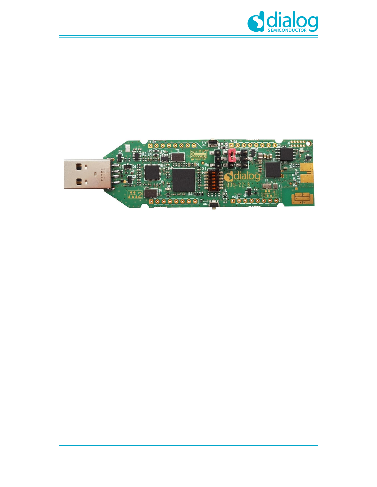
This document describes the DA14695 USB Kit. This kit offers a low-cost development board with
basic functionality. The development kit is implemented on a single PCB. The block diagram, the
actual board, the various sections and settings as well as the connectivity are presented. The
purpose of this cost-effective USB kit is to provide users with the capability of:
● Software development
● Programming DA14695 via JTAG or UART using Dialog's SDK
● Connecting MikroBUS™ modules
Figure 1: DA14695 USB Kit
4 System Overview
4.1 Features
The features of DA14695 USB kit include:
■ Highly integrated DA14695 Bluetooth® Smart SoC from Dialog Semiconductor
■ Access on GPIOs provided from the chip, when no MikroBUS™ is plugged in
■ The ability to be connected directly to PC USB without extra cables
■ Reset push button
■ General purpose LED and button
■ Using USB (5 V), LDO (3.3 V), or external battery as power source
■ JTAG and UART interface over USB via SEGGER
■ 32 Mbit QSPI flash on board
■ 2.4 GHz printed antenna and slot for SMA connector
■ 32 MHz main crystal and 32.768 kHz low-power crystal
■ Low cost
■ Compact design
■ A dimension of 100 mm × 26.5 mm × 11 mm
Page 6
UM-B-103
DA14695 USB Kit
User Manual
Revision 1.0
14-Feb-2019
CFR0012
6 of 34
© 2019 Dialog Semiconductor
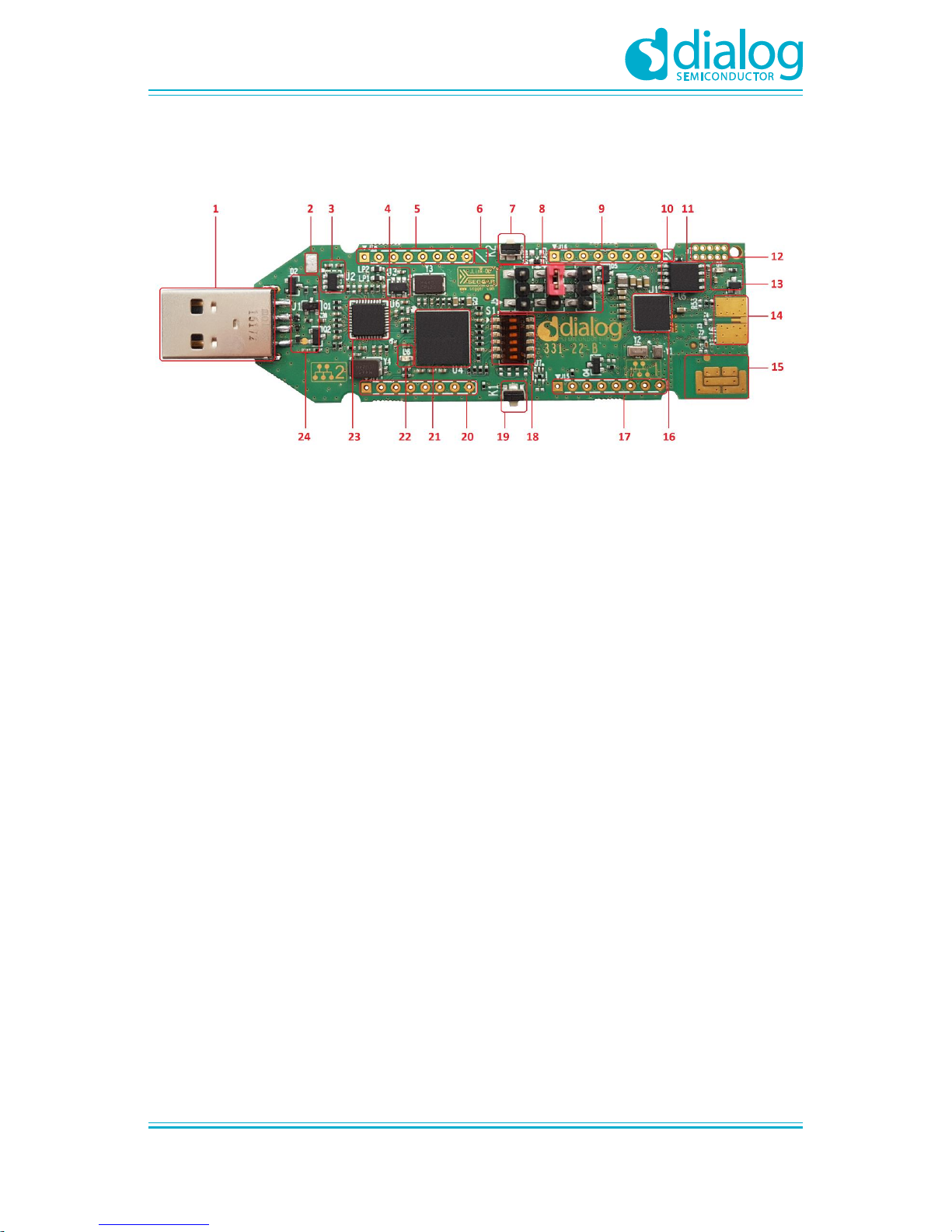
4.2 System and Components Description (Top View)
Figure 2: DA14695 USB Kit - Top Side
The USB kit is based on the DA14695 SoC in an VFBGA86 package. The marked and numbered
sections of the system are:
1. Type-A USB connector (J1)
2. GND support point (not populated)
3. LDO 3.3V (U2)
4. LDO 3.3V (U3)
5. MikroBUS™ slot #2 connection points (Right side - J18, 8 pins)
6. MikroBUS™ slot #2 diagnostical notch (serves as a guideline for add-on board insertion. For
more information, please check MikroBUS™ standard specifications)
7. Reset push button (K2)
8. DA14695 power selection headers (VBUS - J2, VBAT- J3) and battery connector header(J5)
9. MikroBUS™ slot #1 connection points (Right side - J16, 8 pins)
10. MikroBUS™ slot #1 diagnostical notch (serves as a guideline for add-on board insertion. For
more information, please check MikroBUS™ standard specifications)
11. 32 Mbit QSPI Flash (U5)
12. Debugging Connector (J7, CIB can be connected for UART interface access)
13. Red LED (D7)
14. SMA connector (optional - J6)
15. Printed antenna (ANT1)
16. DA14695 Bluetooth® Smart SoC
17. MikroBUS™ slot #1 connection points (Left side - J15, 8 pins)
18. JTAG & UART Switch selection (S1)
19. General purpose push button (K1)
20. MikroBUS™ slot #2 connection points (Left side - J17, 8 pins)
21. UART & JTAG interface (U4)
Page 7
UM-B-103
DA14695 USB Kit
User Manual
Revision 1.0
14-Feb-2019
CFR0012
7 of 34
© 2019 Dialog Semiconductor
22. Green LED (D8)
23. USB HUB (U6)
24. OVP Circuit
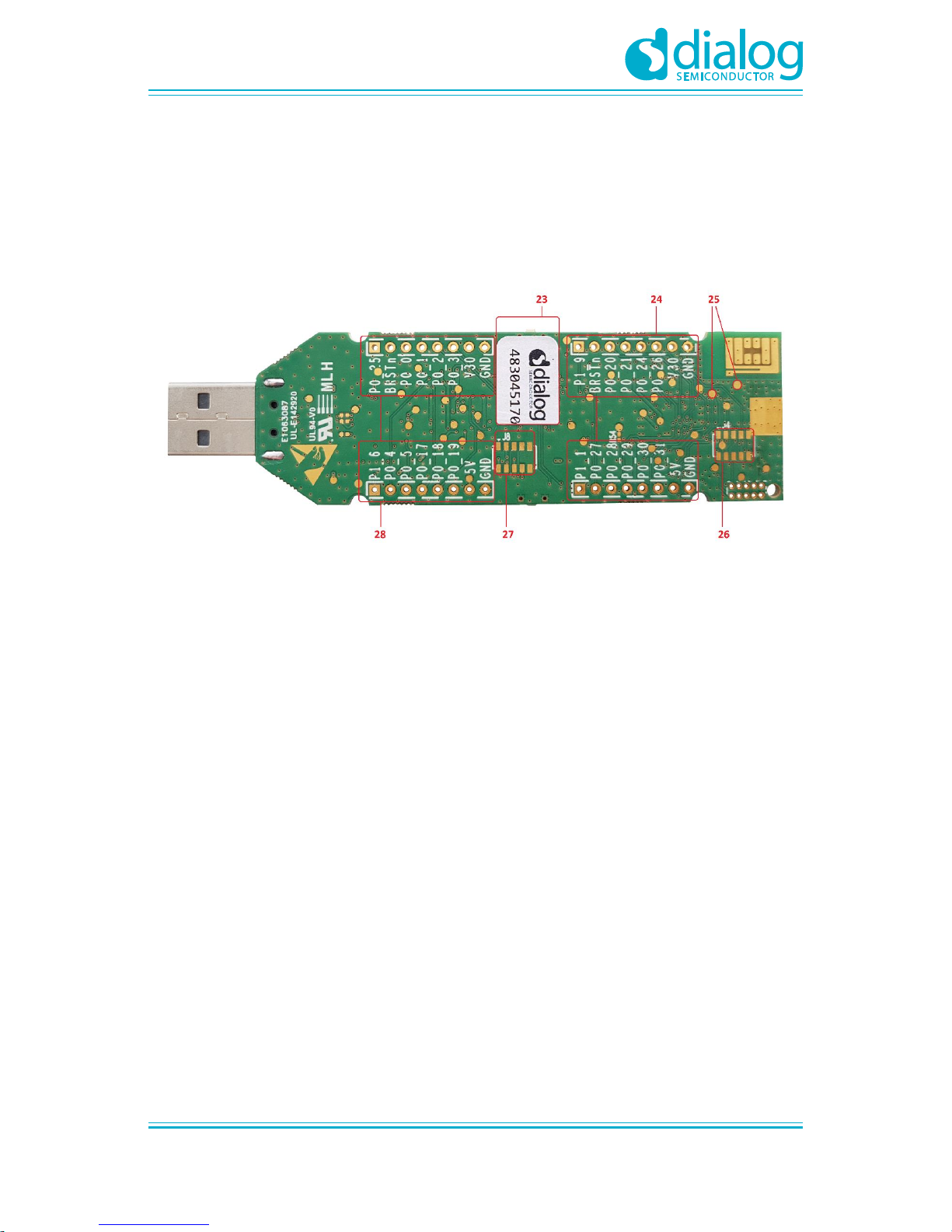
4.3 System and Components Description (Bottom View)
Figure 3: DA14695 USB Kit - Bottom Side
The bottom side of DA14695 USB kit provides information about the MikroBUS™ pins assignment,
the SEGGER ID, and the date code. Test points have been placed for monitoring various signal
behaviors and voltage levels of the components. The marked and numbered sections of the system
are:
23. ID of UART & JTAG interface (U4)
24. MikroBUS™ slot #1 pins assignment
25. Test points (more details in Table 1)
26. GPIO connection header (not populated)
27. QSPI RAM I/O (1.8 V only, not populated)
28. MikroBUS™ slot #2 pins assignment
Page 8
UM-B-103
DA14695 USB Kit
User Manual
Revision 1.0
14-Feb-2019
CFR0012
8 of 34
© 2019 Dialog Semiconductor
4.4 Test Points
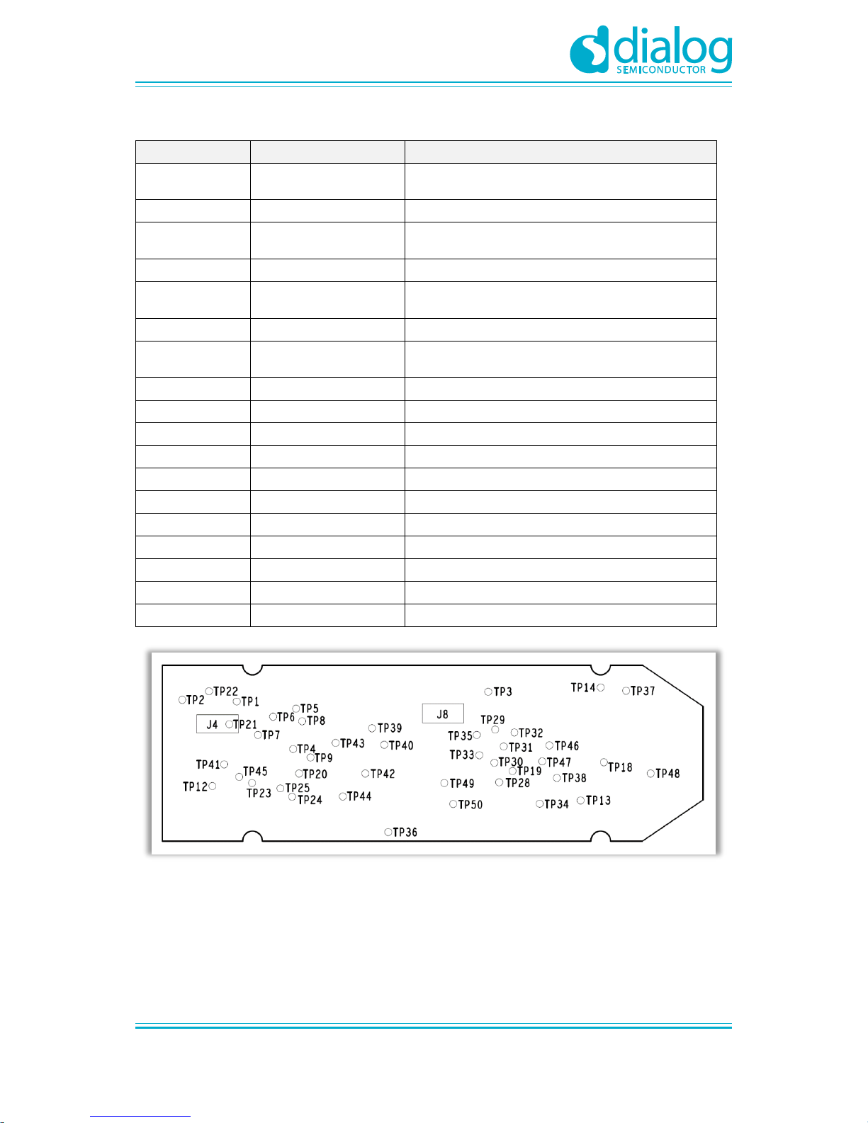
Test points have been placed on the bottom side of the board and allow users to have access to
signals and I/Os, or measure supplies voltage levels. Table 1 shows the assignment for each test
point and Figure 4 shows the topology of the test points.
Table 1: Test Points Assignment
Test Point
Assigned to
Comments
TP1
V18
QSPI data flash supply voltage
TP2
VLED
Voltage level for Red LED
TP3
VBUS
Voltage level for VBUS pin of DA14695
TP4
V30
Voltage level for V30 pin of DA14695
TP5
V18
Voltage level for V18 pin of DA14695
TP6
V18P
Voltage level for V18P pin of DA14695
TP7
V14
Voltage level for V14 pin of DA14695
TP8
V12
Voltage level for V12 pin of DA14695
TP9
VBAT3V
Voltage level for VBAT3V pin of DA14695
TP12
GND
Ground
TP13
GND
Ground
TP14
GND
Ground
TP15
VBUS_IN
USB input voltage level
TP16
ESD_WARNING_LABEL
ESD sensitive device - Not electrically connected
TP17
GND
Ground
TP18
HUB_RST
USB HUB reset pin
TP19
3V3D
LDO 3.3V (U3) output voltage level
TP20
P0_06
General Purpose push button (K1)
TP21
P0_12
MicroBus™ BRSTn
TP22
P0_13
P0_13
TP23
P0_16
P0_16
TP24
P0_22
XTAL32km/P0_22
TP25
P0_23
XTAL32kp/P0_23
TP28
VDD_CORE
Core voltage level of UART & JTAG interface (U4)
TP29
NRST
For programming U4 in production - Not used for
development
TP30
ERASE
For programming U4 in production - Not used for
development
TP31
TMS_SWDIO
For programming U4 in production - Not used for
development
TP32
TCK_SWCLK
For programming U4 in production - Not used for
development
Page 9
UM-B-103
DA14695 USB Kit
User Manual
Revision 1.0
14-Feb-2019
CFR0012
9 of 34
© 2019 Dialog Semiconductor
Test Point
Assigned to
Comments
TP33
SWO/TDO
For programming U4 in production - Not used for
development
TP34
DBLED
Voltage level for Green LED
TP35
SWO/TDO
For programming U4 in production - Not used for
development
TP36
GND
Ground
TP37
VBUS_OUT
Voltage level for VBUS pin of DA14695, when jumper
placed to header J2 (pin 2-3)
TP38
3V3
USB_HUB power supply
TP39
VLDO
Voltage level for VBAT pin of DA14695, when jumper
placed to header J3 (pin 1-2)
TP40
UTX
UART
TP41
RTS
UART
TP42
CTS
UART
TP43
URX
UART
TP44
SWDIO
JTAG
TP45
SWCLK
JTAG
TP46
P0_14
USBDP_2
TP47
P0_15
USBDM_2
TP48
VBUS_IN
USB input voltage level
TP49
SWDIO
JTAG
TP50
SWCLK
JTAG
Figure 4: Test Points Topology (BOTTOM View)
Page 10
UM-B-103
DA14695 USB Kit
User Manual
Revision 1.0
14-Feb-2019
CFR0012
10 of 34
© 2019 Dialog Semiconductor
4.5 Block Diagram
U5
QSPI
Flash
USB_DP/DM
USB_DP/DM_2
JTAG & UART
Swit ch selection
3V3D
VBUS
VBUS_OUT
5V
OVP
3.3V LDO (U3)
32MH z
32KHz
LED (D7) &
Push button (K1)
RSTn
T-Reset
T-Reset
SMA
Connector
MikroBus
#1
J1
Type-A USB
Connector
K2
3V3
U6
USB HUB
MikroBus
#2
3.3V LDO (U2)
VBAT
U4
SEGGER
NTC
J2
J3
J5
S1
NTC
U1
DA14695
3V3
VLDO
BATT
USB_DP_1
USB_DM_1
Printed
ZOR type
Antenna
Figure 5: Block Diagram of DA14695 USB Kit
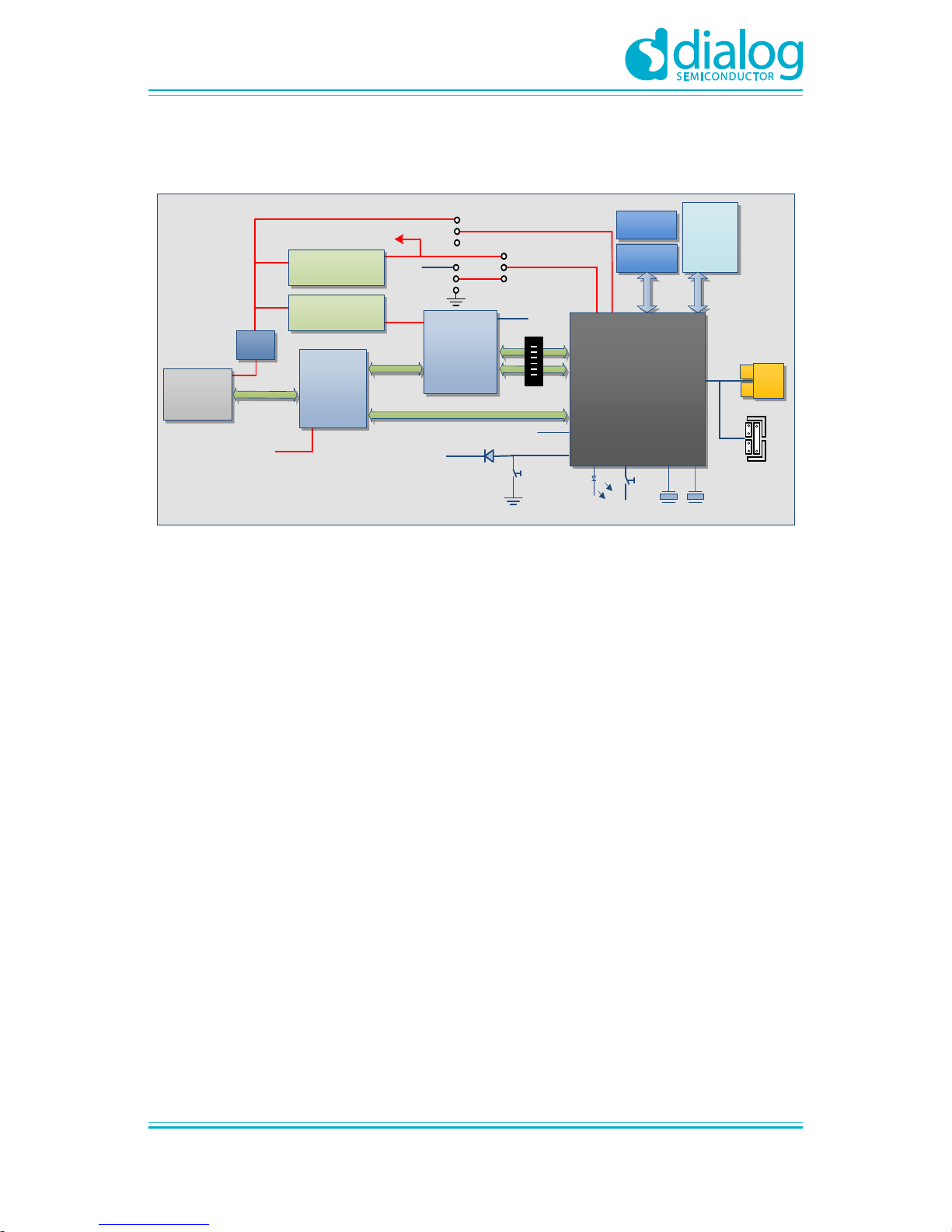
The power of Dialog’s DA14695 SoC on the USB kit can be supplied from three different sources
(Figure 5):
● Default configuration: 5 V provided to VBUS pin, when jumper placed to J2 header (pin 2-3)
● Alternative configuration: 3.3 V provided to VBAT pin, through LDO (U2), when jumper placed to
J3 (pin 1-2)
● Alternative configuration: 3.6 V to 4.3 V provided to VBAT pin, from external LiPo battery
(connected to J5 header), when jumper placed to J3 (pin 2-3)
Page 11

UM-B-103
DA14695 USB Kit
User Manual
Revision 1.0
14-Feb-2019
CFR0012
11 of 34
© 2019 Dialog Semiconductor
5 USB Kit System
5.1 Overview
● Board name/number:
○ DA14695 USB Kit/331-22-C
● SoC:
○ DA14695 in a VFBGA86 package
● Flash memory:
○ MX25U3235F (32 Mbit) QSPI Flash Memory, 8-pin SOIC (200 mil) package
○ 1.8 V (V18P to pin V18F) power supply (default)
● Clock inputs:
○ 32 MHz crystal
○ 32.768 KHz crystal
● Ports:
○ USB port for debugging purposes and battery charging
● Interfaces:
○ UART-JLink CDC UART Port (listed under Ports in Device Manager)
○ JTAG-JLink Driver (listed under Universal Serial Bus Controllers in Device Manager)
● Connectivity-Expansion connectors:
○ Two MikroBUS™ modules can be plugged to J15, J16 and J17, J18 sockets, respectively
(users must solder the sockets manually)
● Power source selection:
○ 5 V on VBUS pin (default)
○ 3.3 V on VBAT via LDO (optional)
○ 3.6 V to 4.3 V from external LiPo battery (optional)
5.2 DA14695 SoC System
The DA14695 is a flexible System-on-Chip (SoC) combining an application processor, an advanced
power management unit, memories, a flexible sensor node controller, a cryptography engine for
enhanced security, digital and analog peripherals, and a new configurable Bluetooth Low Energy
MAC engine with a radio transceiver capable of a 6 dBm output.
The application processor used by DA14695 SoC system is the latest ARM® Cortex® M33™ CPU
which offers up to 144 DMIPS and a RAM of 512 kBytes. This application processor has an 8-region
MPU and a single-precision FPU which enables code execution from embedded memory (RAM) or
external QSPI FLASH via a 16 kB 4-way associative cache controller and the capability of decryption
on-the-fly without extra wait states.
The advanced power management unit of the DA14695 enables it to run from primary and secondary
batteries and provide power to external devices through the SIMO DCDC or integrated LDOs. The
on-chip hardware charger allows the natively rechargeable batteries to be charged over USB.
Page 12
UM-B-103
DA14695 USB Kit
User Manual
Revision 1.0
14-Feb-2019
CFR0012
12 of 34
© 2019 Dialog Semiconductor
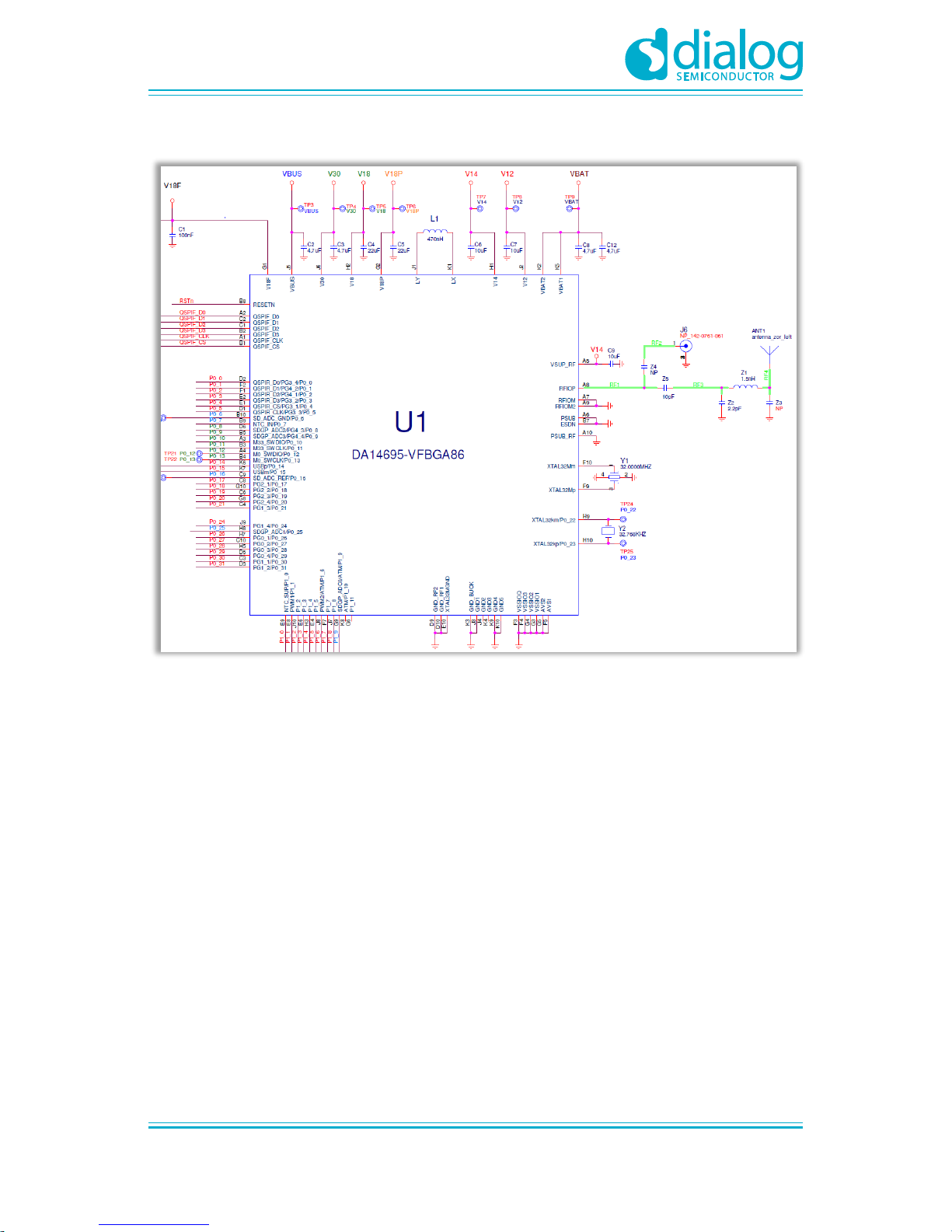
Figure 6: DA14695 Schematic
The DA14695 SoC power management subsystem consists of:
● VBUS: battery charger input as well as USB bus voltage
○ A decoupling capacitor (C2, 0402 package, 6.3 V) equal or less than 4.7 μF is placed close to
VBUS pin
● VBAT1: battery connection
○ It is shorted externally with VBAT2. A 4.7 μF decoupling capacitor (C8, 0402 package, 6.3 V)
is required to be placed close to the pin
○ Voltage range for VBAT1 is 1.7 V to 4.75 V
○ On this development kit, VBAT1 and VBAT2 are connected
● VBAT2: input of the SIMO DC-DC converter
○ It is shorted externally with VBAT1. A 4.7 μF decoupling capacitor (C12, 0402 package, 6.3V)
is required to be placed close to the pin
○ On this development kit, VBAT1 and VBAT2 are connected
● V30: output voltage rail (3 V)
○ A ceramic decoupling capacitor of 4.7 μF (C36, 0402 package, 10 V) is required to be placed
close to the pin
○ V30 cannot be turned off
Page 13

UM-B-103
DA14695 USB Kit
User Manual
Revision 1.0
14-Feb-2019
CFR0012
13 of 34
© 2019 Dialog Semiconductor
○ V30 is the default option for GPIO voltage levels (expect for the QSPI-RAM I/Os which are
fixed to 1.8 V)
○ The current delivery capability of the V30 power rail is 150 mA
○ Overcurrent protection circuit limits the current on V30 if an external device misbehaves
● SIMO DC-DC converter outputs: V18, V18P, V12, and V14.
○ The inductor needed for DC-DC operation is placed externally. A low DCR inductor (L1) of
470 nH (0805 package) is connected on LX/LY pins
○ V18 and V18P: power rails (1.8 V) for supplying external devices, even when the system is in
sleep mode
– Decoupling ceramic capacitors (C4 and C5) of 22 μF (0603 package, 6.3 V), are placed as
close as possible to the V18 and V18P pins.
– V18 is assigned to peripherals devices, QSPI-RAM, and through register setting for GPIOs
– V18P is assigned to external QSPI Data Flash
– The current delivery capability of the V18 and V18P power rails is 50 mA in active mode
○ V12: power rail that supplies the digital core of DA14695 and delivers up to 50 mA at 1.2 V in
active mode. It should not be used to supply external devices
– A 10 μF decoupling capacitor (C7, 0603 package, 6.3 V) is placed close to V12 pin
○ V14: power rail that delivers up to 20 mA at 1.4 V and should not be used for supplying
external devices
– A 10 μF decoupling capacitor (C6, 0603 package, 6.3 V) is placed close to the V14 pin
● VSUP_RF: radio supply voltage
○ It is connected to V14 externally. A 10 μF capacitor (C9, 0603 package, 6.3 V) is placed as
close to the VSUP_RF pin as possible.
Page 14
UM-B-103
DA14695 USB Kit
User Manual
Revision 1.0
14-Feb-2019
CFR0012
14 of 34
© 2019 Dialog Semiconductor
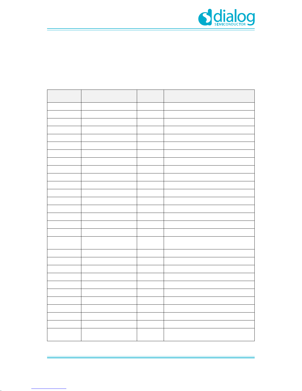
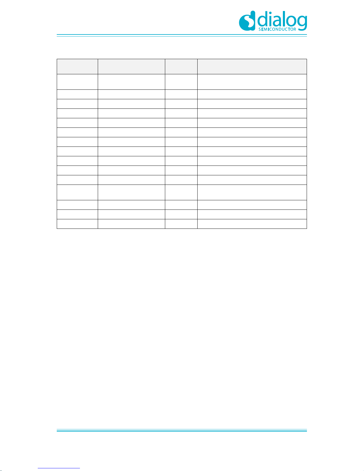
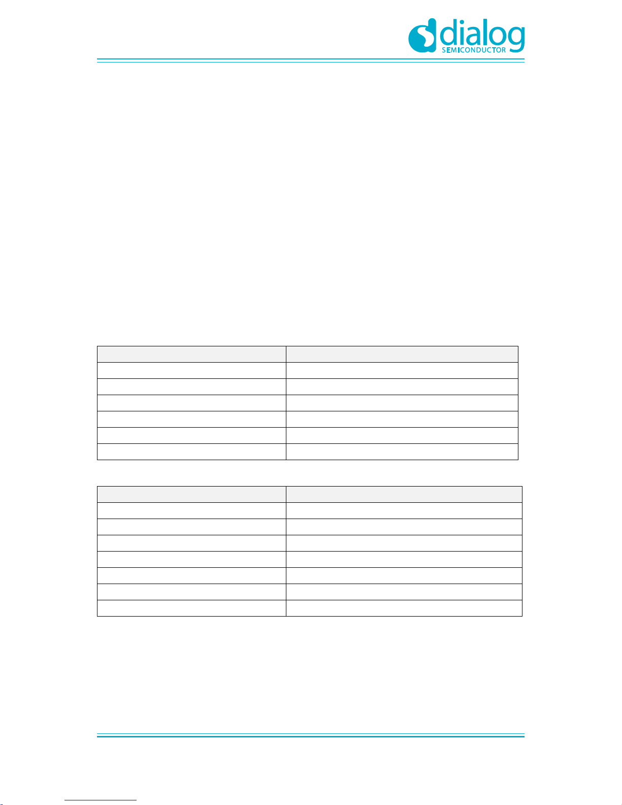
5.3 DA14695 Pin Assignment
Most of the available signals are utilized or extracted on the breakout connectors.
Table 2 provides the pin assignment of the breakout connectors on the USB kit and the related pin
name on the VFBGA86 package of the DA14695.
Table 2: USB Kit Pin Assignment
AQFN60 Pin
Name
Development Kit Signal
Header
Pin
Comments
P0_00
P0_00
J8.3
GPIO
P0_01
P0_01
J8.4
GPIO
P0_02
P0_02
J8.5
GPIO
P0_03
P0_03
J8.6
GPIO
P0_04
P0_04
J8.7
GPIO
P0_05
P0_05
J8.8
GPIO
P0_06
P0_06
-
General Purpose push button (K1)
P0_07
CTS - UART interface
P0_08
URX
-
UART interface
P0_09
UTX - UART interface
P0_10
SWDIO
-
JTAG interface
P0_11
SWCLK
-
JTAG interface
P0_12
P0_12
J15.2/J17.2
MikroBUS™ BRSTn (slot 1,2)
P0_13
P0_13
-
GPIO
P0_14
USBDP_2
-
USB Data plus (+)
P0_15
USBDM_2
-
USB Data minus (-)
P0_16
P0_16
-
GPIO
P0_17
GPIO/MB2_TX
J18.4
GPIO/MikroBUS™ Universal Asynchronous
Transmitter (slot 2)
P0_18
GPIO/MB2_SCL
J18.5
GPIO/MikroBUS™ I2C SCL (slot 2)
P0_19
GPIO/MB2_SDA
J18.6
GPIO/MikroBUS™ I2C SDA (slot 2)
P0_20
GPIO/MB1_CS
J15.3
GPIO/MikroBUS™ CS (slot 1)
P0_21
GPIO/MB1_SCK
J15.4
GPIO/MikroBUS™ SCK (slot 1)
P0_22
XTAL32M
-
XTAL 32.768 kHz minus (-)
P0_23
XTAL32P
-
XTAL 32.768 kHz plus (+)
P0_24
GPIO/MB1_MISO
J15.5
GPIO/MikroBUS™ MISO (slot 1)
P0_25
GPIO/MB2_AN
J17.1
GPIO/MikroBUS™ Analog (slot 2)
P0_26
GPIO/MB1_MOSI
J15.6
GPIO/MikroBUS™ MOSI (slot 1)
P0_27
GPIO/MB1_INT
J16.2
GPIO/MikroBUS™ Interrupt (slot 1)
P0_28
GPIO/MB1_RX
J16.3
GPIO/MikroBUS™ Universal Asynchronous
Receiver (slot 1)
Page 15
UM-B-103
DA14695 USB Kit
User Manual
Revision 1.0
14-Feb-2019
CFR0012
15 of 34
© 2019 Dialog Semiconductor
AQFN60 Pin
Name
Development Kit Signal
Header
Pin
Comments
P0_29
GPIO/MB1_TX
J16.4
GPIO/MikroBUS™ Universal Asynchronous
Transmitter (slot 1)
P0_30
GPIO/MB1_SCL
J16.5
GPIO/MikroBUS™ I2C SCL (slot 1)
P0_31
GPIO/MB1_SDA
J16.6
GPIO/MikroBUS™ I2C SDA (slot 1)
P1_00
RTS
J4.3
UART interface
P1_01
GPIO/MB_PWM/RED_LED
J16.2/J4.4
GPIO/MikroBUS™ I2C PWM (slot 1)/Red LED
P1_02
GPIO/MB2_CS
J17.3/J4.5
GPIO/MikroBUS™ CS (slot 2)
P1_03
GPIO/MB2_SCK
J17.4/J4.6
GPIO/MikroBUS™ SCK (slot 2)
P1_04
GPIO/MB2_MISO
J17.5/J4.7
GPIO/MikroBUS™ MISO (slot 2)
P1_05
GPIO/MB2_MOSI
J17.6/J4.8
GPIO/MikroBUS™ MOSI (slot 2)
P1_06
GPIO/MB2_PWM
J18.1
GPIO/MikroBUS™ PWM (slot 2)
P1_07
GPIO/MB2_INT
J18.2
GPIO/MikroBUS™ interrupt (slot 2)
P1_08
GPIO/MB2_RX
J18.3
GPIO/MikroBUS™ Universal Asynchronous
Receiver (slot 2)
P1_09
GPIO/MB1_AN
J15.1
GPIO/MikroBUS™ Analog (slot 1)
P1_10
- - Not connected
P1_11
- - Not connected
Page 16
UM-B-103
DA14695 USB Kit
User Manual
Revision 1.0
14-Feb-2019
CFR0012
16 of 34
© 2019 Dialog Semiconductor
5.4 Booting from UART
There is only one boot loader option for booting from UART using pins P0_9 (T_TX) and P0_8
(T_RX). Please note that UART-booting does not support hardware handshake signals (RTS/CTS).
The settings for UART booting are:
● Baud rate 115.2 kbps
● 8 bits
● No parity
● 1 stop bit
For more details on booting with UART, check application note AN-B-052 ([2]).
5.5 Crystals
The DA14695 SoC has two Digitally Controlled Crystal Oscillators, one at 32 MHz (XTAL32M) and
the other at 32.768 kHz (XTAL32K). XTAL32K has no trimming capabilities and is used as the clock
of the Extended/Deep Sleep modes, while XTAL32M can be trimmed.
The crystals used on the USB kit are specified in Table 3 and Table 4.
Table 3: Y1 (32 MHz crystal) characteristics
Reference Designator
Value
Part Number
XRCGB32M000F1H00R0
Frequency
32 MHz
Accuracy
±10 ppm
Load Capacitance (CL)
6 pF
Equivalent Series Resistance (ESR)
60 Ω
Drive Level (PD)
150 μW
Table 4: Y2 (32.768 kHz crystal) characteristics
Reference Designator
Value
Part Number
ABS07-32.768KHZ-7-T
Frequency
32.768 kHz
Accuracy
±20 ppm
Load Capacitance (CL)
12.5 pF
Shunt Capacitance (C0)
0.9 - 1.2 pF
Equivalent Series Resistance (ESR)
100 Ω
Drive Level (PD)
0.1 μW
Page 17
UM-B-103
DA14695 USB Kit
User Manual
Revision 1.0
14-Feb-2019
CFR0012
17 of 34
© 2019 Dialog Semiconductor
5.6 Antenna and RF Port
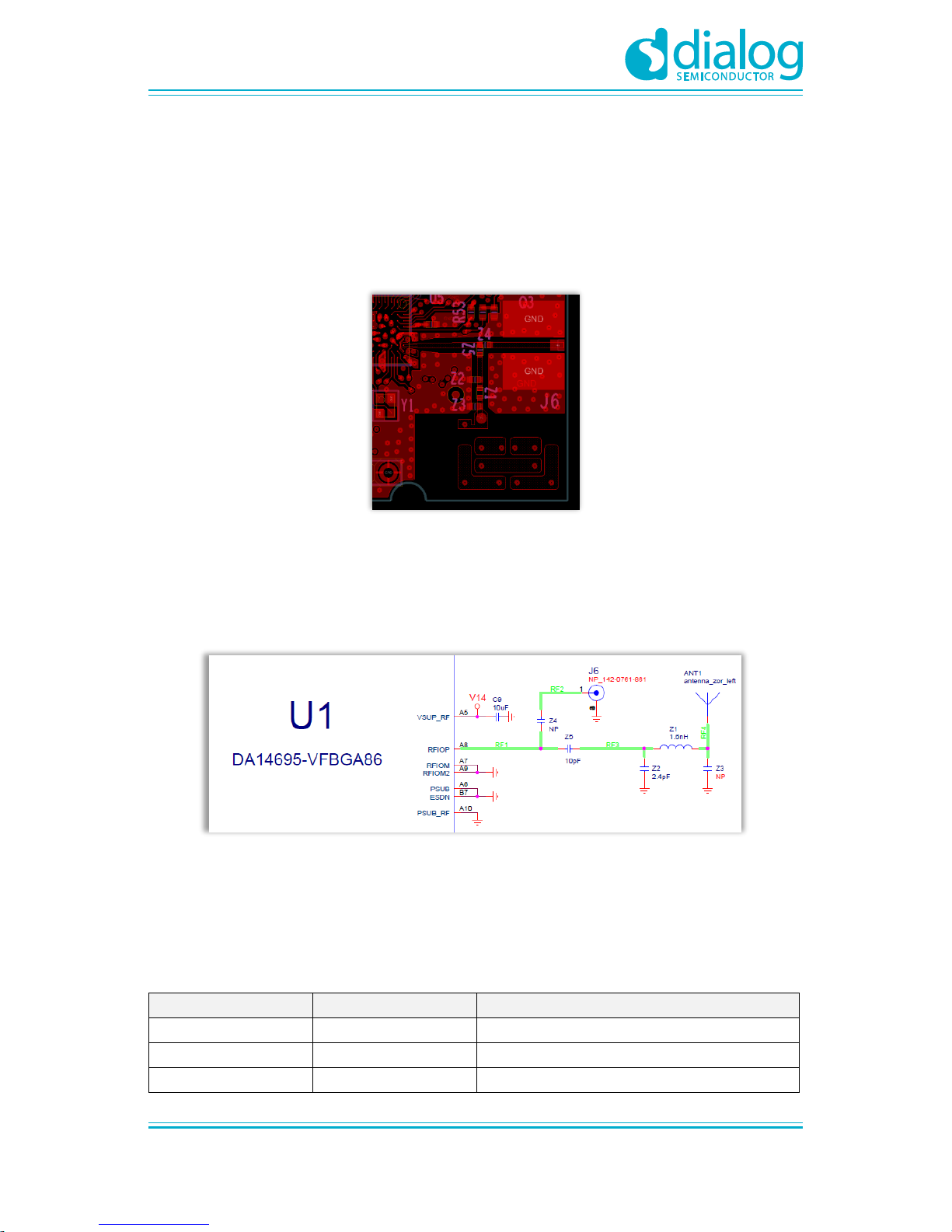
A printed type antenna is currently used as the default antenna in the DA14695 USB Kit. The
DA14695 USB Kit provides a single-ended RFIO port matched to 50 Ω. The RF port consists of the
RFIOp, RFIOm, and RFIOm2 pins, of which RFIOm and RFIOm2 are connected to ground. A copper
trace with an impedance of 50 Ω interconnects the RF port and the printed antenna (ANT1). A Pi-
network (Z1, Z2, and Z3) is added for antenna matching purposes.
Figure 7: RF Matching Circuit, Printed Antenna, and SMA Connector
The DA14695 USB Kit provides an RF connector (no populated) in parallel with the SMD chip
antenna. The RF connector can be used for conducted RF evaluation/testing. The RF connector type
is 142-0761-861. To perform RF measurements using the RF connector J6, users must remove the
capacitor Z5 (10 pF) and place the capacitor Z4 (10 pF).
Figure 8: RF Port, RF Connector, RF Matching, and SMD Chip Antenna
5.6.1 RF Measurements and Antenna Matching
RF measurements have been performed to increase the efficiency of the ANT1. The values of the RF
components are shown in Table 5.
Table 5: RF Components Names and Values
Component Name
Component Value
Manufacturer Part Number
Z1
1.6 nH
LQP15MN1N5W02D
Z2
2.4 pF
GJM1555C1H2R4BB01D
Z3 - Not populated
Page 18
UM-B-103
DA14695 USB Kit
User Manual
Revision 1.0
14-Feb-2019
CFR0012
18 of 34
© 2019 Dialog Semiconductor
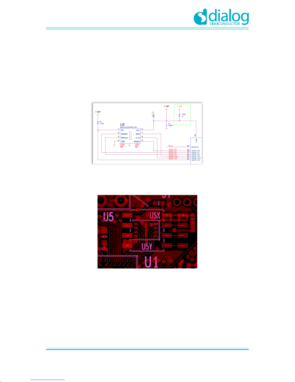
5.7 QSPI Data Flash Memory (U5)
The DA14695 USB Kit includes an external QSPI Data Flash memory from Macronix. The
MX25U3235F Flash memory supports the standard Serial Peripheral Interface (SPI), Dual/Quad I/O
SPI as well as 2-clock instruction cycle Quad Peripheral Interface (QPI), Serial Clock, Chip Select,
Serial Data I/O0 (DI), I/O1(D0), I/O2 (/WP), and I/O3(/HOLD).
The selected QSPI flash for the DA14695 USB Kit is MX25U3235FM2I-10G in 8-pin SOIC 208mil
package (U5). DA14695 USB Kit can support QSPI Data flash with 8-pin SOIC 150mil package
(U5Y) or QSPI Data flash with 8-pin USON (2x3) package (U5X), as shown in Figure 10.
Figure 9: QSPI Data Flash
The DA14695 uses the external Flash memory for directly executing code with some help from the
internal cache, or simply for mirroring the contents in RAM during booting.
Figure 10: Available packages for QSPI Data Flash
Page 19
UM-B-103
DA14695 USB Kit
User Manual
Revision 1.0
14-Feb-2019
CFR0012
19 of 34
© 2019 Dialog Semiconductor
5.8 Reset Circuit
Figure 11: Reset Circuit
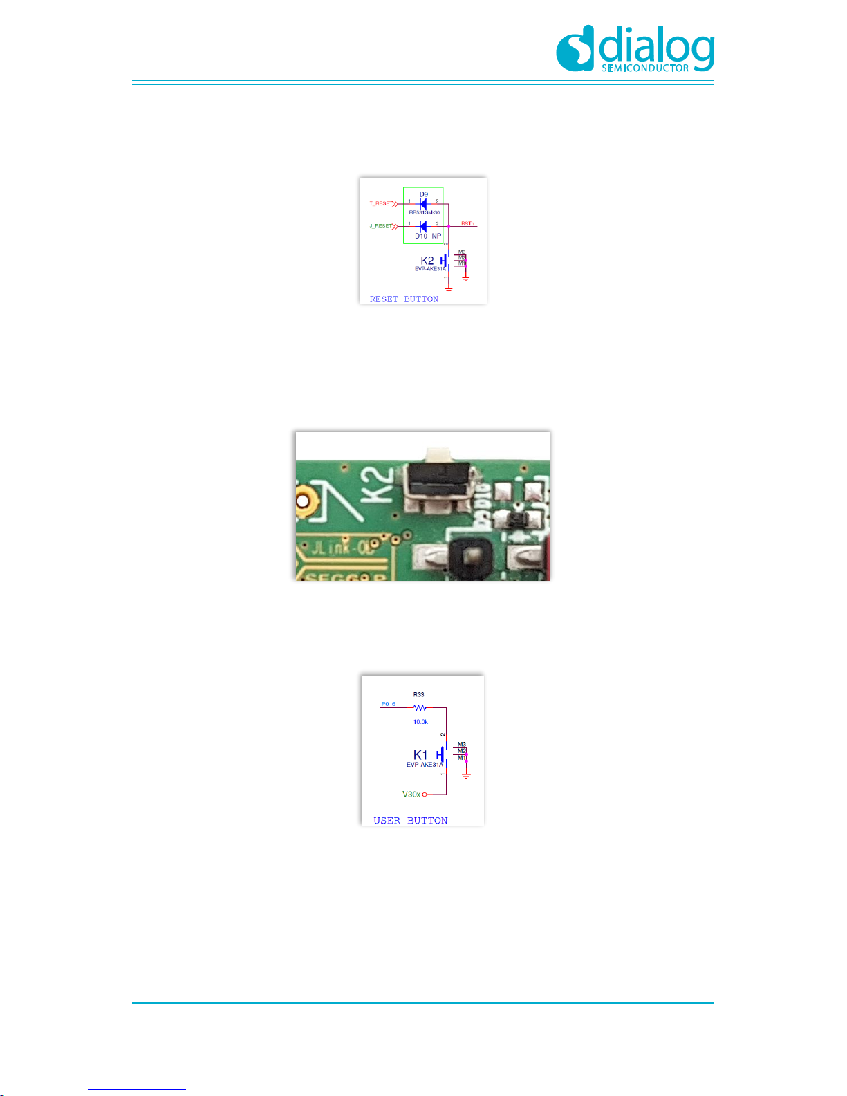
The DA14695 comprises an RSTn pad which is active low. The DA14695 USB Kit can be reset by
pressing the on-board RESET push button (K2, Figure 12) or through software from the UART &
JTAG interface processor (U4, Figure 2, #21). The Reset push button drives the RSTn pad to the
ground.
Figure 12: RESET Push Button (K2)
5.9 General Purpose Push Button
Figure 13: General Purpose Push Button
General purpose push button K1 is connected to P0_06 (Figure 13). It is populated and placed on
the top side of the board (Figure 14).
Page 20
UM-B-103
DA14695 USB Kit
User Manual
Revision 1.0
14-Feb-2019
CFR0012
20 of 34
© 2019 Dialog Semiconductor
Figure 14: General Purpose Push Button K1 (Populated at TOP)
5.10 Debugging Port DIP Switch
Figure 15: Debugging DIP Switch
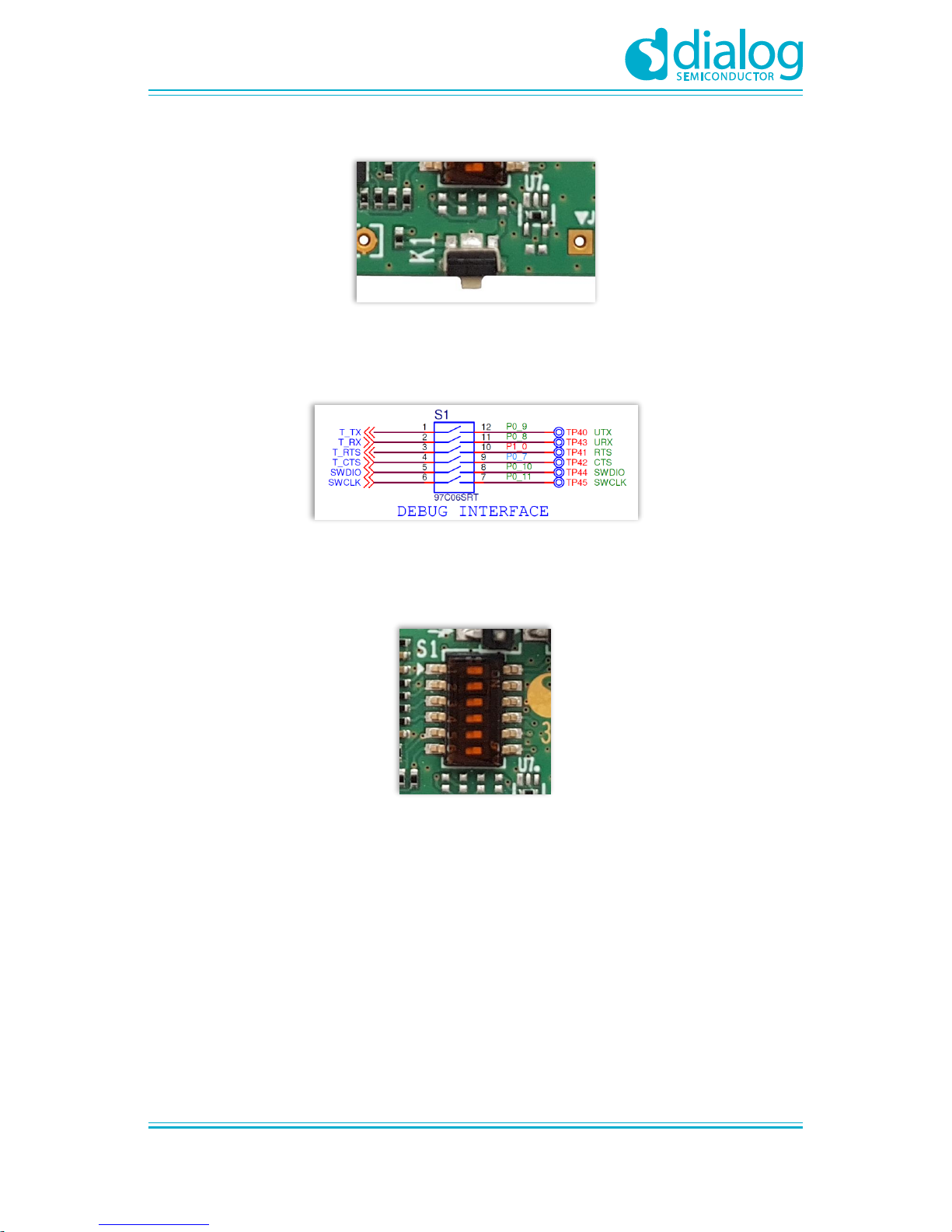
S1 is a DIP switch which allows users to disconnect the pins used for debugging (default state is all
pins connected) to allow accurate deep sleep power measurement.
Figure 16: Debugging DIP switch
Page 21
UM-B-103
DA14695 USB Kit
User Manual
Revision 1.0
14-Feb-2019
CFR0012
21 of 34
© 2019 Dialog Semiconductor
5.11 User Controlled LED
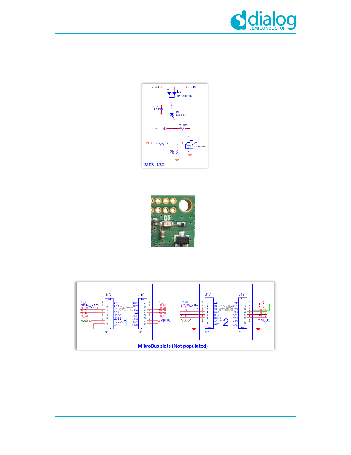
The red LED D7 that can be controlled by users is driven from P1_1 (Figure 17).
Figure 17: General Purpose Red LED
Figure 18: General Purpose Red LED D7
5.12 MikroBUS™ Modules
Figure 19: Mikrobus™ Pin Assignment
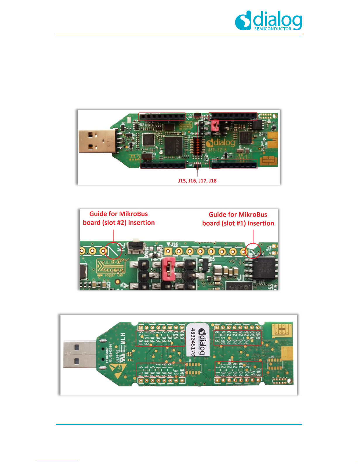
The DA14695 USB Kit can support MikroBUS™ modules. Users must place and solder J15, J16
sockets (for slot #1) and/or J17, J18 sockets (for slot #2) on the top side of the board as shown in
Figure 20. A possible female socket type is PPTC081LFBN-RC.
Page 22
UM-B-103
DA14695 USB Kit
User Manual
Revision 1.0
14-Feb-2019
CFR0012
22 of 34
© 2019 Dialog Semiconductor
Figure 21 shows the diagnostic silkscreen, below the right-hand side pinout, which serves as a
guideline for add-on board insertion. For more information, please check MikroBus™ standard
specifications. The pin assignment is printed at the bottom side of the DA14695 USB Kit (Figure 22).
A MikroBUS™ module requires a power supply of 5 V, 3.3 V, or both, depending on the module. The
voltage for the 5.0 V MikroBUS™ pins is taken directly from the main USB connector. The voltage of
the 3.3 V MikroBUS™ pins is powered from V30 through the overcurrent protection circuit.
Figure 20: J15, J16, J17, and J18 Female Sockets (Must Be Soldered by Users)
Figure 21: Guides for Proper Mikrobus™ Click Boards Insertion
Figure 22: Mikrobus™ Pin Assignment
Page 23
UM-B-103
DA14695 USB Kit
User Manual
Revision 1.0
14-Feb-2019
CFR0012
23 of 34
© 2019 Dialog Semiconductor
5.13 GND Test Point
On this test point, users can connect oscilloscope's ground probe.
Figure 23: GND Support Point
Figure 24: GND Support Point (Must Be Placed by Users)
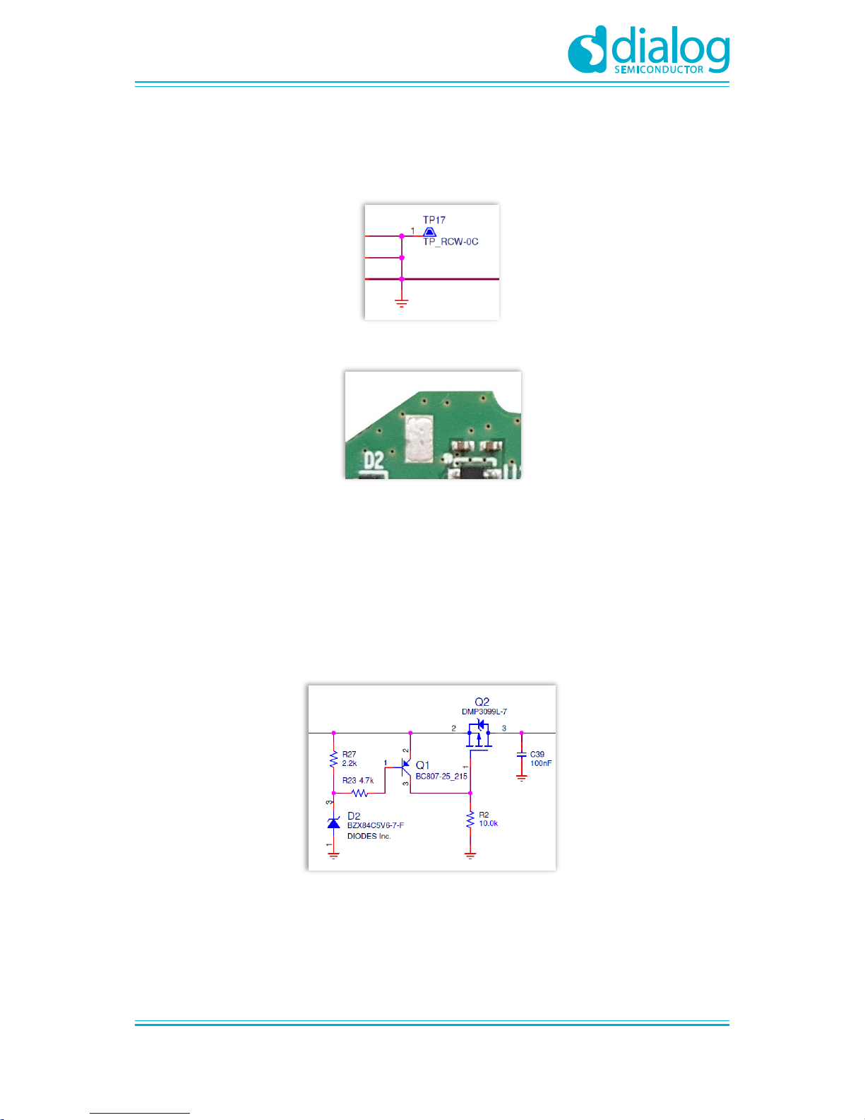
5.14 Over Voltage Protection Circuit (OVP)
The DA14695 USB Kit can be used as a portable standalone device. The power supply can be a
power-bank or a mobile charger. The overvoltage protection circuit OVP circuit can protect the device
from overvoltage of up to 20 V. Figure 25 shows a schematic of the OVP circuit. Overvoltage is
caused not only by the connection of an unsuitable charger with different characteristics, but also
from voltage surges caused by insertion of long length cable. For normal operation of the DA14695
USB Kit, the input voltage range should be between 4.75 V and 5.25 V, as required by the USB
standard.
Figure 25: Over Voltage Protection Circuit
Page 24
UM-B-103
DA14695 USB Kit
User Manual
Revision 1.0
14-Feb-2019
CFR0012
24 of 34
© 2019 Dialog Semiconductor
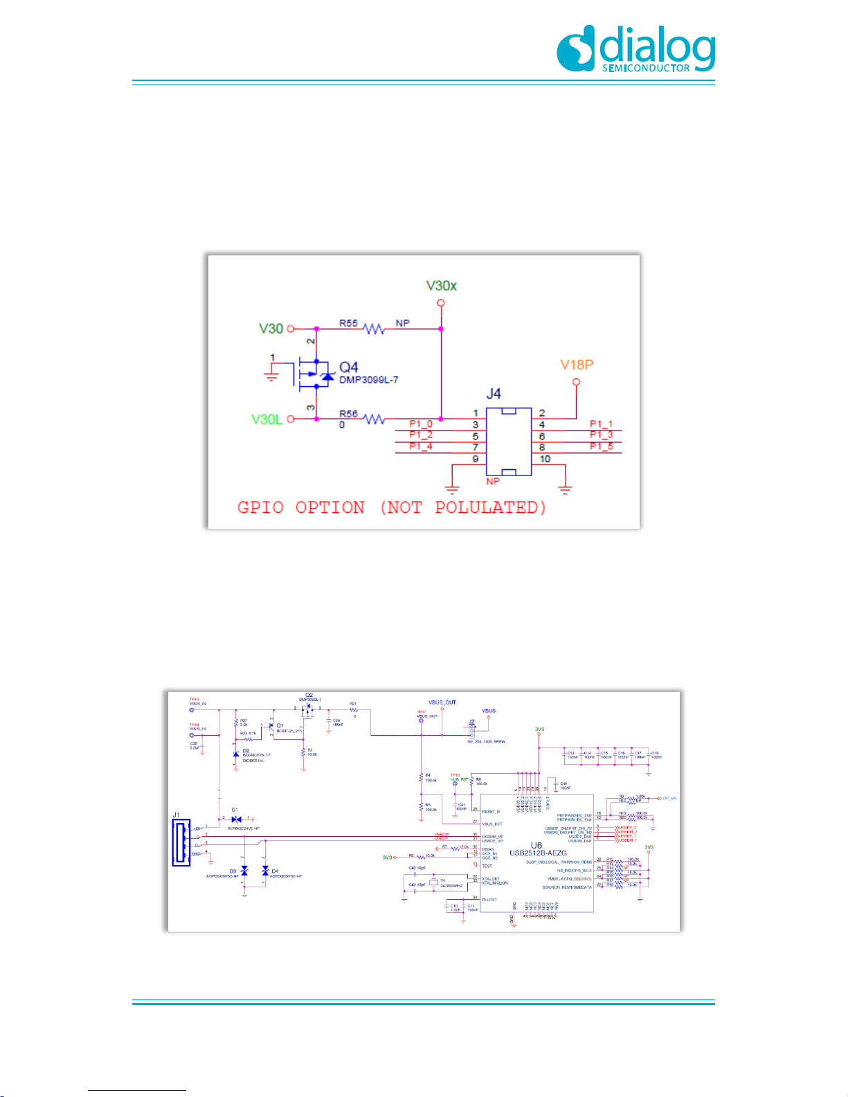
5.15 Over-Current Protection Circuit on V30 Power Rail
A P-FET is added in series with V30 power rail to prevent the voltage on the pin from dropping to
very low levels if a peripheral surge sets an overcurrent condition.
The voltage on V30L (external peripherals) may reach low levels, but the voltage on V30 (the pin)
always stays above 2 V.
Figure 26: Over Current Protection Circuit on V30 Power Rail
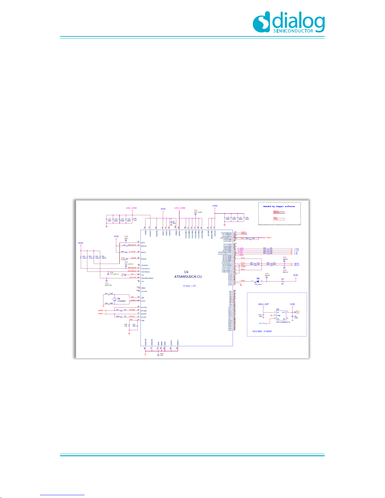
5.16 USB HUB
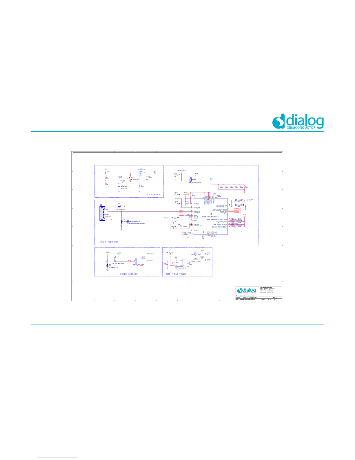
USB HUB is implemented by U6, USB2512B-AEZG. This chip is supplied with a voltage of 3.3 V
from U2. The signal LDO_EN is generated from U6 and it is an active high signal. It enables the LDO
(U3) which supplies the U4 (debugging). A 24 MHz crystal (Y4) is required for the chip operation.
Figure 27 shows the circuit's schematic.
Figure 27: USB HUB Circuitry
Page 25
UM-B-103
DA14695 USB Kit
User Manual
Revision 1.0
14-Feb-2019
CFR0012
25 of 34
© 2019 Dialog Semiconductor
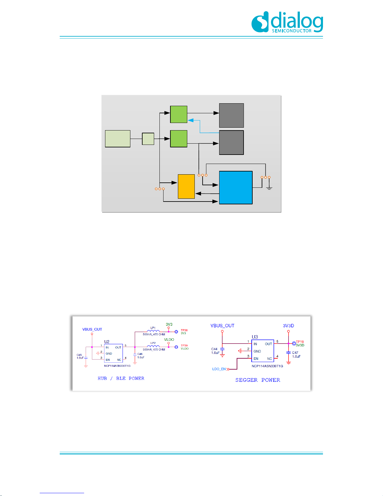
5.17 Debugging Processor (U4)
Two debugging options (JTAG/UART) are available on the DA14695 SoC.
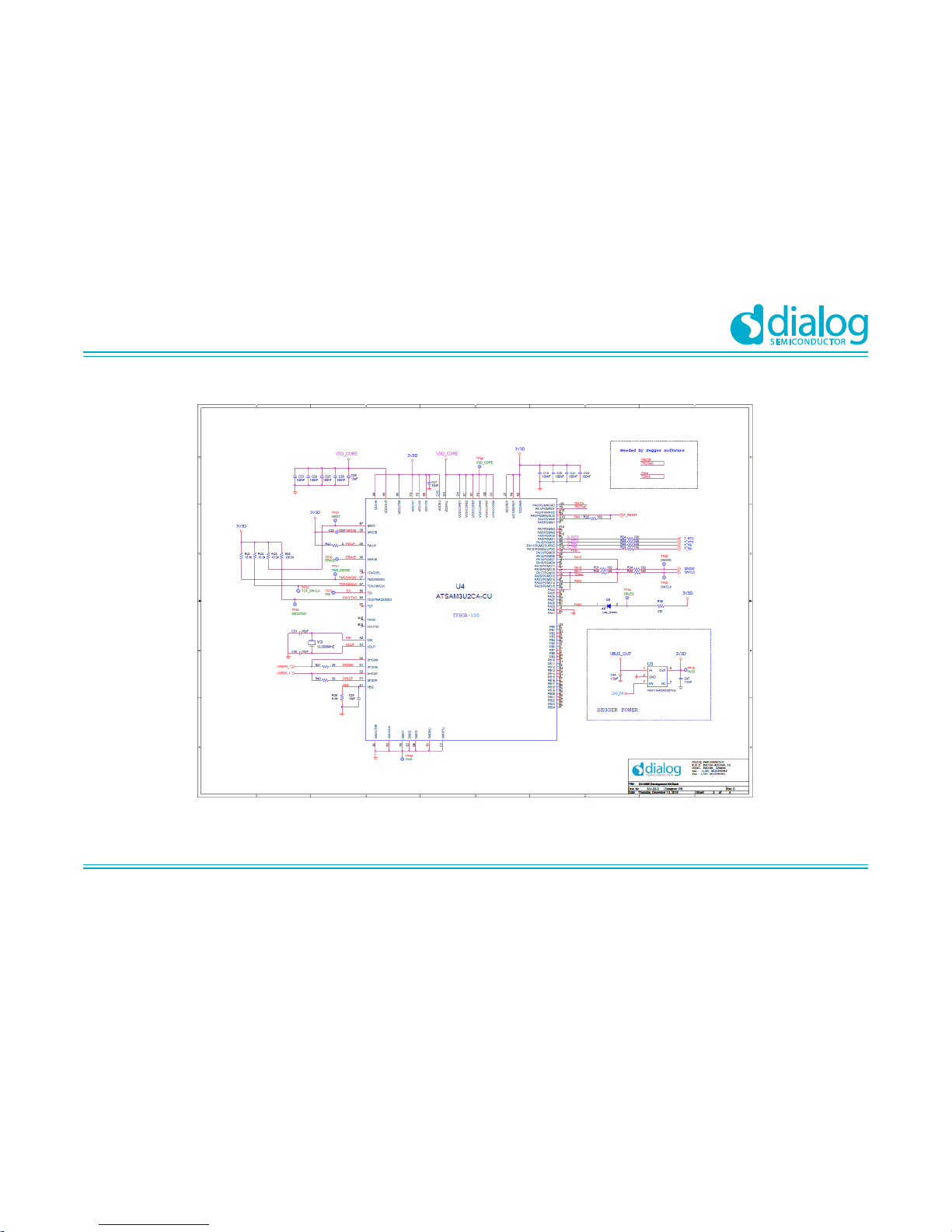
The USB-to-JTAG and USB-to-UART functions are implemented by the SAM3U2CA processor (U4)
(Figure 28), running the Segger JLink-OB firmware. The functions served by U4 are:
● Connecting PC to DA14695 JTAG port
● Connecting PC to DA14695 UART (2-pin or 4-pin)
● Reset DA14695 through the T_RESET line
The UART port supports hardware flow control (RTS/CTS). It is detected automatically by the J-LinkOB firmware, regardless of the setting on the host machine terminal. The behavior of the UART
interface depends on the implementation in the J-Link-OB firmware and is subject to changes by
SEGGER Microcontroller © with updates to the firmware. See [2] for troubleshooting possible issues
with the serial port.
The JTAG operating status is indicated via the green LED D8. The SAM3U2CA (U4) chip is supplied
with a voltage of 3.3 V from U3. A 12 MHz crystal (Y3) is required for the chip operation. Figure 28
shows the circuit's schematic.
Figure 28: Debugging Processor UART And JTAG Interface (U4)
Page 26
UM-B-103
DA14695 USB Kit
User Manual
Revision 1.0
14-Feb-2019
CFR0012
26 of 34
© 2019 Dialog Semiconductor
5.18 Power Section
The DA14695 USB Kit is supplied from 5 V to VBUS pin via J2 header (jumper has been placed to
connect pins 2-3). Figure 29 shows the power tree.
USB
Port
U2
LDO
3.3V
U3
LDO
3.3V
Mikro
Bus
Segger
DA14695
5V
3V3D
VLDO
BATT
VBAT
NTC
3V3
V30
VBUS
OVP
VBUS_OUT
LDO_EN
USB HUB
J2
J5
J3
Figure 29: DA14695 USB Kit Power Tree
The following power components are placed on the DA14695 USB Kit:
● U2: fixed output 3.3 V LDO
○ It generates 3V3 voltage rail that supplies USB HUB and power section header J3
● U3: fixed output 3.3 V LDO
○ It generates 3V3D voltage rail that supplies the USB to JTAG/UART chip (U4,
ATSAM3U2CA-CU)
○ It is enabled from USB HUB through the signal LDO_EN
○ If the USB HUB is not enumerated with an external device (PC, Laptop, and so on), the LDO
is not enabled. Consequently, the debugging circuit is not functional.
Figure 30: Linear Voltage Regulators (LDOs) U2 And U3
Page 27
UM-B-103
DA14695 USB Kit
User Manual
Revision 1.0
14-Feb-2019
CFR0012
27 of 34
© 2019 Dialog Semiconductor
5.19 Power Selection Headers
The DA14695 USB Kit allows users to power supply the DA14695 from three different sources:
● 5 V to VBUS pin (default)
● 3.3 V to VBAT pin (optional)
● 3.6 V to 4.2 V from external battery to VBAT pin (optional)
The default power configuration for DA14695 is from VBUS 5 V via power selection header J2. A
jumper has been placed to pins 2-3 of the J2 header. There is capability to power supply DA14695
either from LDO or external battery. Power configuration selection depends on the SDK project
configuration as well. Changes to Dialog’s SDK might be needed, depending on the SDK project and
the power supply of DA14695 (supplied from VBUS, VBAT, or battery). There are four different
power configurations (Table 6) where users must plug or remove jumpers to J2, J3, J5 headers.
Table 6: DA14695 Power Configurations
Power configuration
J2
J3
J5
LDO (3.3 V)
-
Jumper to 1-2
-
VBUS (5 V) (default)
Jumper to 2-3
-
-
External Battery (3.6 V to 4.2 V)
-
Jumper to 2-3
Battery connection
Charging external Battery
Jumper to 2-3
Jumper to 2-3
Battery connection
Note 1 If the battery has an extra pin for NTC (measuring battery’s temperature), then R30 = 5.6 kΩ must be
placed by the user.
Note 2 If DA14695 is supplied from an external battery but the USB Kit is not connected to USB port, there is
a leakage current through UART and JTAG signals. Users must disconnect these signals by turning
OFF the switches in S1 (section 5.105.10).
Page 28
UM-B-103
DA14695 USB Kit
User Manual
Revision 1.0
14-Feb-2019
CFR0012
28 of 34
© 2019 Dialog Semiconductor
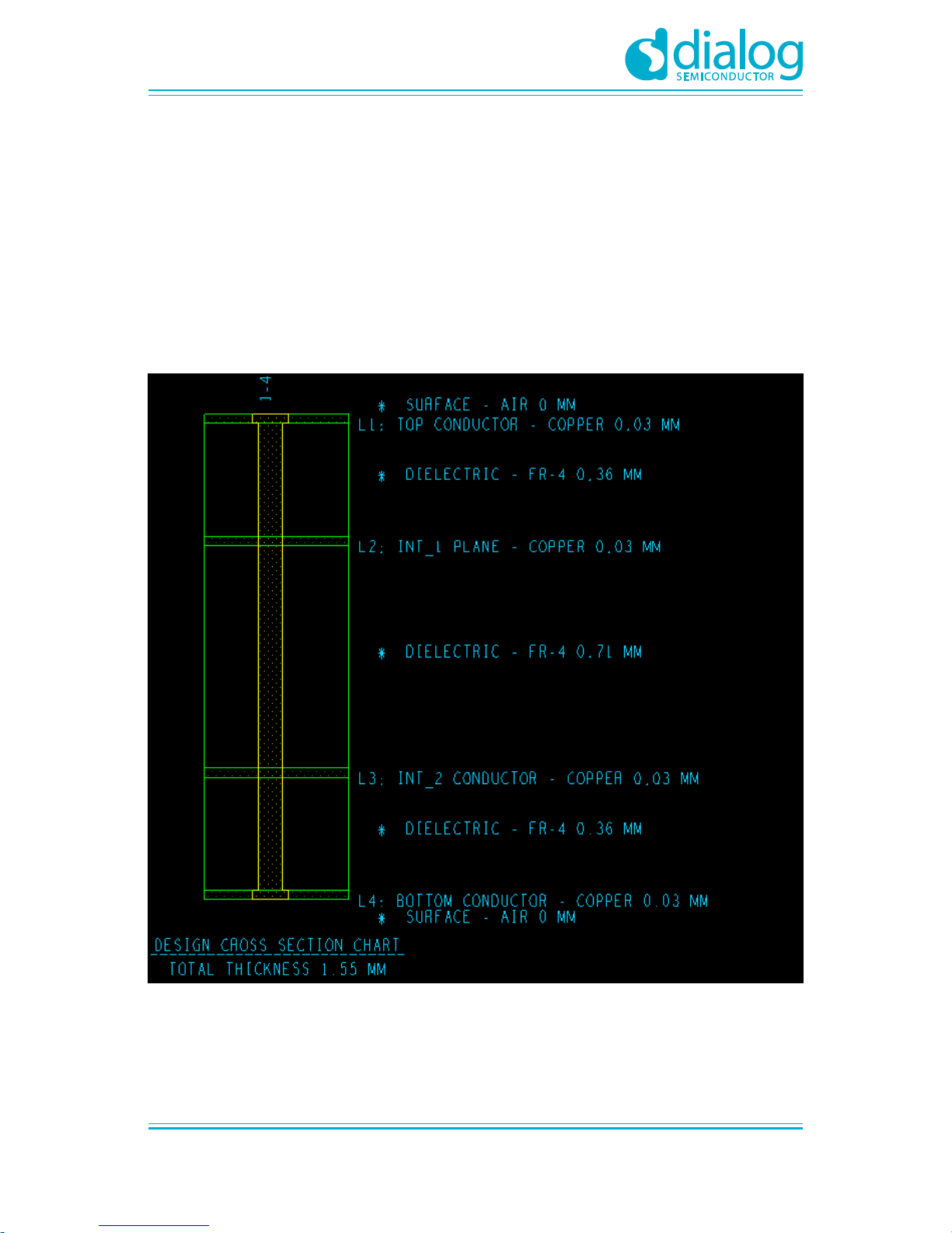
6 PCB Layout
Dimensions: 100 mm × 26.5 mm × 11 mm
Number of layers: 4
PCB thickness: 1.55 mm
Material: FR-4
Solder mask TOP/BOTTOM: Green
Silkscreen TOP/BOTTOM: White
Surface finish: Che Ni/Au
Figure 31: PCB Cross Section
The total thickness of the board is 1.55 mm. The dielectric between each layer is shown in Figure 31.
Page 29
UM-B-103
DA14695 USB Kit
User Manual
Revision 1.0
14-Feb-2019
CFR0012
29 of 34
© 2019 Dialog Semiconductor
Appendix A Schematics
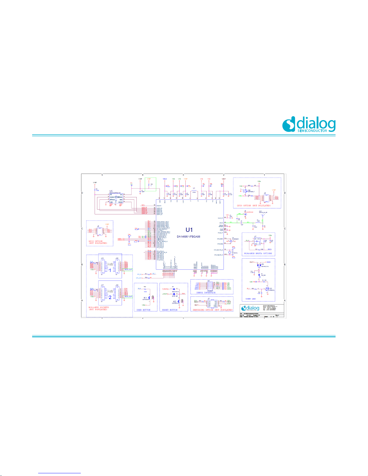
Figure 32: DA14695 SoC Section
Page 30
UM-B-103
DA14695 USB Kit
User Manual
Revision 1.0
14-Feb-2019
CFR0012
30 of 34
© 2019 Dialog Semiconductor
Figure 33: UART & JTAG Interface Chip Section
Page 31
UM-B-103
DA14695 USB Kit
User Manual
Revision 1.0
14-Feb-2019
CFR0012
31 of 34
© 2019 Dialog Semiconductor
Figure 34: USB Hub Section
Page 32
UM-B-103
DA14695 USB Kit
User Manual
Revision 1.0
14-Feb-2019
CFR0012
32 of 34
© 2019 Dialog Semiconductor
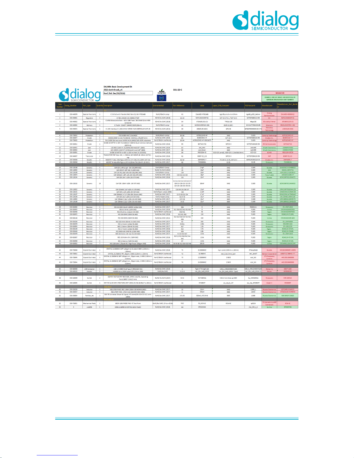
Appendix B Bill of Materials
Figure 35: Bill of Materials (BOM)
Page 33

UM-B-103
DA14695 USB Kit
User Manual
Revision 1.0
14-Feb-2019
CFR0012
33 of 34
© 2019 Dialog Semiconductor
Revision History
Revision
Date
Description
1.0
14-Feb-2019
Initial version.
Page 34
UM-B-103
DA14695 USB Kit
User Manual
Revision 1.0
14-Feb-2019
CFR0012
34 of 34
© 2019 Dialog Semiconductor
Status Definitions
Status
Definition
DRAFT
The content of this document is under review and subject to formal approval, which may result in modifications or
additions.
APPROVED
or unmarked
The content of this document has been approved for publication.
Disclaimer
Information in this document is believed to be accurate and reliable. However, Dialog Semiconductor does not give any representations or
warranties, expressed or implied, as to the accuracy or completeness of such information. Dialog Semiconductor furthermore takes no
responsibility whatsoever for the content in this document if provided by any information source outside of Dialog Semiconductor.
Dialog Semiconductor reserves the right to change without notice the information published in this document, including without limitation the
specification and the design of the related semiconductor products, software and applications.
Applications, software, and semiconductor products described in this document are for illustrative purposes only. Dialog Semiconductor makes
no representation or warranty that such applications, software and semiconductor products will be suitable for the specified use without further
testing or modification. Unless otherwise agreed in writing, such testing or modification is the sole responsibility of the customer and Dialog
Semiconductor excludes all liability in this respect.
Customer notes that nothing in this document may be construed as a license for customer to use the Dialog Semiconductor products, software
and applications referred to in this document. Such license must be separately sought by customer with Dialog Semiconductor.
All use of Dialog Semiconductor products, software and applications referred to in this document are subject to Dialog Semiconductor’s Standard
Terms and Conditions of Sale, available on the company website (www.dialog-semiconductor.com) unless otherwise stated.
Dialog and the Dialog logo are trademarks of Dialog Semiconductor plc or its subsidiaries. All other product or service names are the property of
their respective owners.
© 2019 Dialog Semiconductor. All rights reserved.
Contacting Dialog Semiconductor
United Kingdom (Headquarters)
Dialog Semiconductor (UK) LTD
Phone: +44 1793 757700
Germany
Dialog Semiconductor GmbH
Phone: +49 7021 805-0
The Netherlands
Dialog Semiconductor B.V.
Phone: +31 73 640 8822
North America
Dialog Semiconductor Inc.
Phone: +1 408 845 8500
Japan
Dialog Semiconductor K. K.
Phone: +81 3 5769 5100
Taiwan
Dialog Semiconductor Taiwan
Phone: +886 281 786 222
Hong Kong
Dialog Semiconductor Hong Kong
Phone: +852 2607 4271
Korea
Dialog Semiconductor Korea
Phone: +82 2 3469 8200
China (Shenzhen)
Dialog Semiconductor China
Phone: +86 755 2981 3669
China (Shanghai)
Dialog Semiconductor China
Phone: +86 21 5424 9058
Email:
Web site:
www.dialog-semiconductor.com
 Loading...