

Page 1

User Manual
DA14585 Voice RCU Hardware
Manual
UM-B-087
Abstract
This document describes the hardware design of the DA14585 Voice RCU reference design (Rev.B),
which is based on the Dialog Semiconductor DA14585 Bluetooth® low energy SoC. This reference
design includes an accelerometer/gyro sensor, digital microphone, keypad, and a trackpad which is
placed on a separate daughterboard.
Page 2

UM-B-087
DA14585 Voice RCU Hardware Manual
User Manual
Revision 1.0
09-Jun-2017
CFR0012
2 of 34
© 2017 Dialog Semiconductor
Contents
Abstract ................................................................................................................................................ 1
Contents ............................................................................................................................................... 2
Figures .................................................................................................................................................. 3
Tables ................................................................................................................................................... 3
1 Terms and Definitions ................................................................................................................... 4
2 References ..................................................................................................................................... 4
3 Introduction.................................................................................................................................... 4
4 System Overview ........................................................................................................................... 5
4.1 Features ................................................................................................................................ 5
4.2 Block Diagram ....................................................................................................................... 5
4.3 PCBA Overview .................................................................................................................... 6
5 DA14585 Voice RCU Reference Design ...................................................................................... 9
5.1 DA14585 SoC ....................................................................................................................... 9
5.2 Pin Assignment ................................................................................................................... 10
5.3 Power Management ............................................................................................................ 11
5.4 Flash Memory ..................................................................................................................... 11
5.5 Crystal Oscillators ............................................................................................................... 12
5.6 Microphone ......................................................................................................................... 13
5.7 Capacitive Touch Controller ................................................................................................ 14
5.8 Accelerometer/Gyroscope Sensor ...................................................................................... 15
5.9 Infrared LED ........................................................................................................................ 16
5.10 Buzzer 16
5.11 ON/OFF Switch ................................................................................................................... 17
5.12 LEDs 17
5.13 Reset Button ....................................................................................................................... 18
5.14 Keypad Matrix ..................................................................................................................... 18
5.15 Printed Antenna .................................................................................................................. 19
6 Schematics................................................................................................................................... 20
7 PCB Layout .................................................................................................................................. 22
8 Power Measurements ................................................................................................................. 24
9 Enclosure ..................................................................................................................................... 26
10 Configuration of the Debugging Interface ................................................................................ 29
10.1 Debug/Programming Interface Scenarios ........................................................................... 32
10.1.1 Scenario 1: RCU Inside the Enclosure ................................................................ 32
10.1.2 Scenario 2: RCU Outside the Enclosure ............................................................. 32
Revision History ................................................................................................................................ 33
Page 3

UM-B-087
DA14585 Voice RCU Hardware Manual
User Manual
Revision 1.0
09-Jun-2017
CFR0012
3 of 34
© 2017 Dialog Semiconductor
Figures
Figure 1: Top Level Block Diagram of the DA14585 Voice RCU Reference Design ............................ 5
Figure 2: DA14585 Voice RCU Reference Design (Rev B) - Top View ................................................ 6
Figure 3: DA14585 Voice RCU Reference Design (Rev B) - Bottom View ........................................... 6
Figure 4: Trackpad Daughterboard (Rev B) – Top View ....................................................................... 7
Figure 5: Trackpad Daughterboard (Rev B) – Bottom View .................................................................. 7
Figure 7: Complete DA14585 Voice RCU Reference Design (Rev B) with Track Wheel ..................... 8
Figure 6: Complete DA14585 Voice RCU Reference Design (Rev B) with Trackpad .......................... 8
Figure 8: DA14585 System Schematic ................................................................................................. 9
Figure 9: Serial NOR Flash Memory ................................................................................................... 11
Figure 10: SPK0838HT4H Microphone Schematic ............................................................................. 13
Figure 11: Capacitive Touch Controller Schematic (Trackpad) .......................................................... 14
Figure 12: Capacitive Touch Controller Schematic (Wheel) ............................................................... 14
Figure 13: BMI160- Inertial Sensor Schematic.................................................................................... 15
Figure 14: IR LED Schematic .............................................................................................................. 16
Figure 15: Buzzer Schematic .............................................................................................................. 16
Figure 16: Power ON/OFF Switch Schematic ..................................................................................... 17
Figure 17: Indication LEDs Schematic ................................................................................................ 17
Figure 18: Reset Button Schematic and Actual Illustration ................................................................. 18
Figure 19: Keypad Matrix Schematic .................................................................................................. 18
Figure 20: PCB view of a printed antenna ........................................................................................... 19
Figure 21: Printed Antenna Radiation Pattern..................................................................................... 19
Figure 22: DA14585 Voice RCU Reference Design Rev. B1 - SoC, Flash Memory, Debugging Port 20
Figure 23: DA14585 Voice RCU Reference Design Rev. B1 – Peripherals, Sensors ........................ 21
Figure 24: DA14585 Voice RCU Reference Design Rev. B - Top View ............................................. 22
Figure 25: DA14585 Voice RCU Reference Design Rev. B - Bottom View ........................................ 23
Figure 26: DA14585 Voice RCU Reference Design - PCB Stack-Up ................................................. 23
Figure 27: DA14585 Voice RCU Reference Design – Average Operating Current ............................ 24
Figure 28: DA14585 Voice RCU Reference Design – Average Sleep Current ................................... 24
Figure 29: DA14585 Voice RCU Reference Design – Average Touch Pad Scanning Current .......... 25
Figure 30: DA14585 Voice RCU Reference Design – Current during Touch Pad Scan Pulse .......... 25
Figure 31: DA14585 Voice RCU Reference Design Enclosure – Top View ....................................... 26
Figure 32: DA14585 Voice RCU Reference Design Enclosure – Bottom View .................................. 26
Figure 33: Connection of JTAG Cable with DA14585 Voice RCU PCB Inside Enclosure .................. 27
Figure 34: Connection of CIB Board with DA14585 Voice RCU PCB inside the Enclosure ............... 27
Figure 35: DA14585 Voice RCU Reference Design Enclosure – Top Exploded View ....................... 28
Figure 36 : DA14585 Voice RCU Reference Design Enclosure - Side Exploded View ...................... 28
Figure 37: Debug Interface .................................................................................................................. 29
Figure 38: IDC-10 Programming/Debugging Cable Installation .......................................................... 29
Figure 39: Communication Interface Board (CIB) ............................................................................... 30
Figure 40: Connection of the DA14585 Voice RCU PCB to the CIB Programming Board ................. 31
Figure 41: Power ON/OFF Switch Position for Scenario 1 (Green Arrow: ON) .................................. 32
Figure 42: Power ON/OFF Switch Position for Scenario 2 (Green Arrow: JTAG) .............................. 32
Tables
Table 1: DA14585 Voice RCU Reference Design Rev. B - Pin Assignment ...................................... 10
Table 2: Y1 (16 MHz Crystal) Characteristics ..................................................................................... 12
Table 3: Y2 (32 kHz Crystal) Characteristics ...................................................................................... 12
Table 4: BMI160 Inertial Sensor - Electrical Characteristics ............................................................... 15
Table 5: Printed Antenna Performance Characteristics ...................................................................... 19
Table 6: DA14585 Voice RCU Reference Design ............................................................................... 25
Page 4

UM-B-087
DA14585 Voice RCU Hardware Manual
User Manual
Revision 1.0
09-Jun-2017
CFR0012
4 of 34
© 2017 Dialog Semiconductor
1 Terms and Definitions
APDU Application Protocol Data Unit
BLE Bluetooth low energy
BOM Bill Of Materials
CIB Communication Interface Board
DCXO Digitally Controlled Crystal Oscillator
ESR Equivalent Series Resistance
HW hardware
IFA Inverted-F Antenna
IR InfraRed
JTAG Joint Test Action Group (test interface)
LED Light Emitting Diode\
PCM Pulse Code Modulation
PDM Pulse Density Modulation
RCU Remote Control Unit
RF Radio Frequency
SoC System On Chip
SPI Serial Peripheral Interface
UART Universal Asynchronous Receiver/Transmitter
USB Universal Serial Bus
2 References
[1] DA14585 datasheet, Dialog Semiconductor.
[2] Application Note : ''Designing Printed Antennas for Bluetooth® Low Energy''
3 Introduction
Bluetooth low energy remote control units (RCU) are becoming the standard in next-generation
Smart TVs and set-top boxes as they improve the user experience by enabling 2-way communication
as well as non-line-of-sight communication to control equipment that is placed behind a door or a
piece of furniture, or in another room.
The Dialog Voice RCU reference design builds on its best-in-class Bluetooth low energy solution, the
DA14585, to deliver an RCU with world-leading battery lifetime and a very small Bill of Materials.
Page 5
UM-B-087
DA14585 Voice RCU Hardware Manual
User Manual
Revision 1.0
09-Jun-2017
CFR0012
5 of 34
© 2017 Dialog Semiconductor
4 System Overview
4.1 Features
■ Highly integrated Dialog Semiconductor DA14585 Bluetooth® Smart SoC
■ Stand-alone module
■ Low BOM due to printed antenna
■ Low cost PCB
■ Integrated keypad
■ Combined accelerometer/gyroscope sensor unit
■ Separate trackpad/wheel modules
■ Access to processor via JTAG and UART from the enclosure
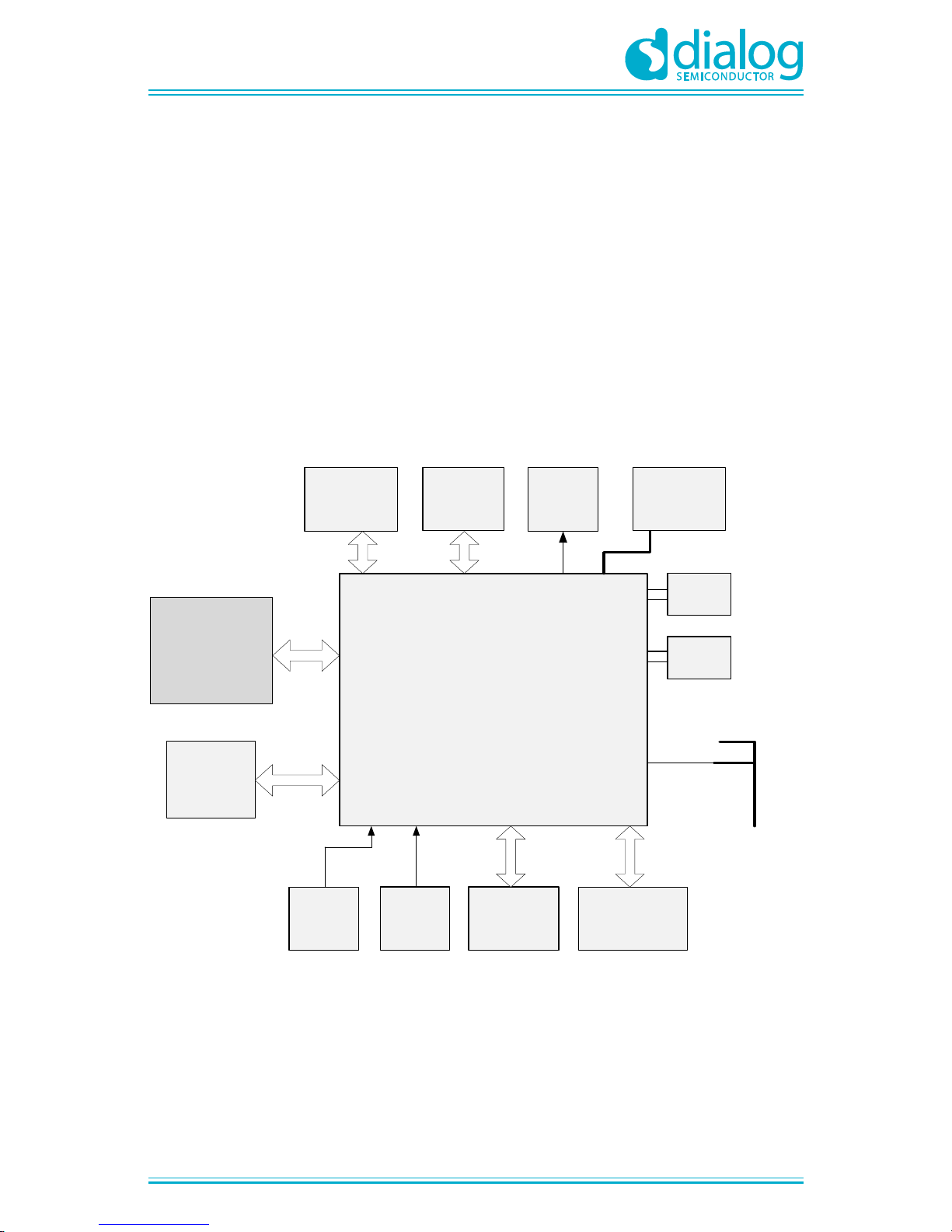
4.2 Block Diagram
DA14585
Keypad
Flash
Memory
Buzzer
BMI160
Accelerometer/
Gyro
Microphone
Battery
Reset
Button
On/Off
Switch
Debugging
Header
XTAL
32 kHz
XTAL
16 MHz
SPI
Row 1-4
Col 1-3
JTAG
UART
SPI
Printed
Antenna
VBAT
Trackpad/Wheel
Daughterboard
incl. Azoteq
Touch Controller
(IQS572)
I2C
PDM
Figure 1: Top Level Block Diagram of the DA14585 Voice RCU Reference Design
Page 6
UM-B-087
DA14585 Voice RCU Hardware Manual
User Manual
Revision 1.0
09-Jun-2017
CFR0012
6 of 34
© 2017 Dialog Semiconductor
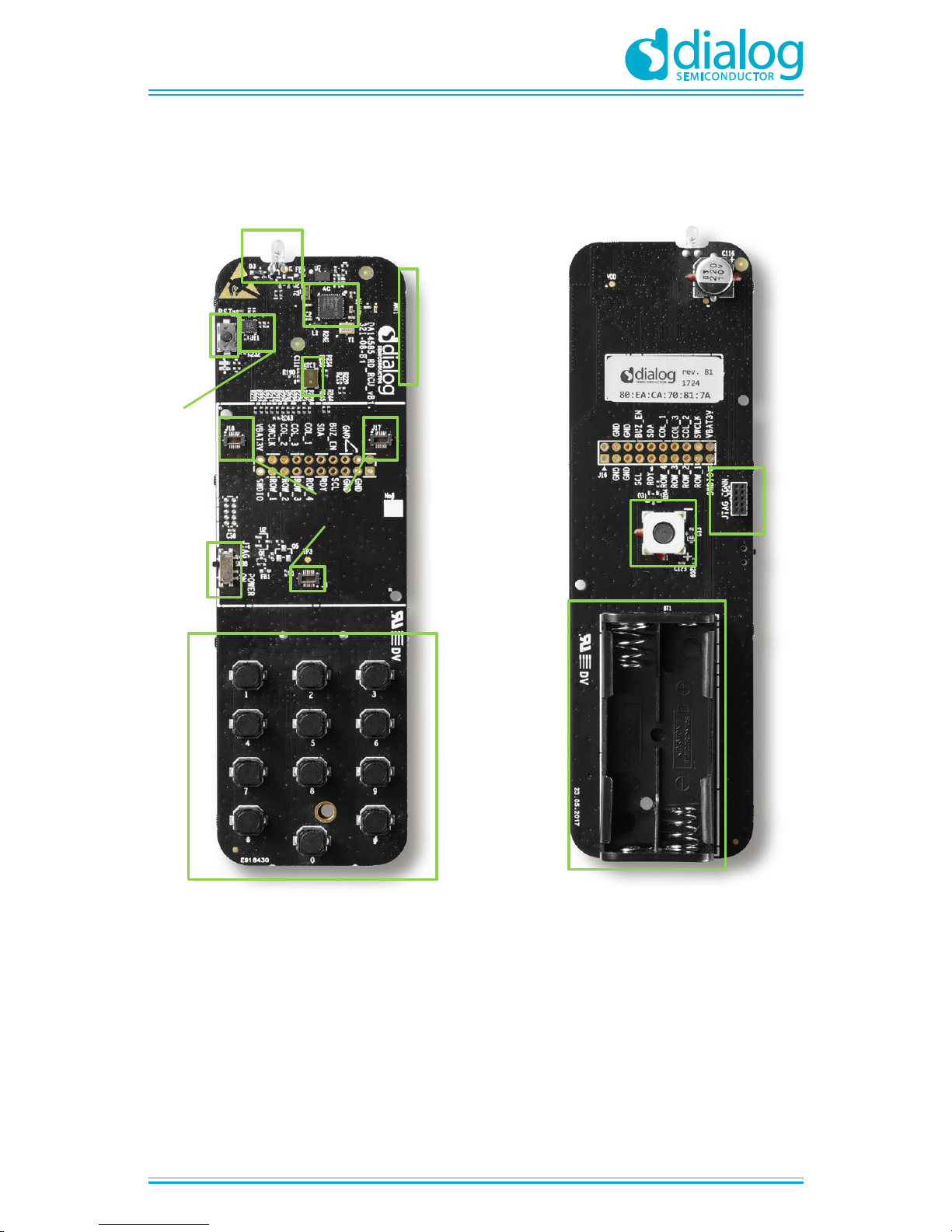
4.3 PCBA Overview
IR LED
DA14585
Reset
Button
MIC
Trackpad
sockets
Power
On/OFF
switch
Keypad
BMI160
Accelerometer
/Gyro
ANT1
AAA
Battery
Holder
Figure 2: DA14585 Voice RCU
Reference Design (Rev B) -
Top View
Figure 3: DA14585 Voice RCU
Reference Design (Rev B) -
Bottom View
Buzzer
JTAG
connector
Page 7
UM-B-087
DA14585 Voice RCU Hardware Manual
User Manual
Revision 1.0
09-Jun-2017
CFR0012
7 of 34
© 2017 Dialog Semiconductor
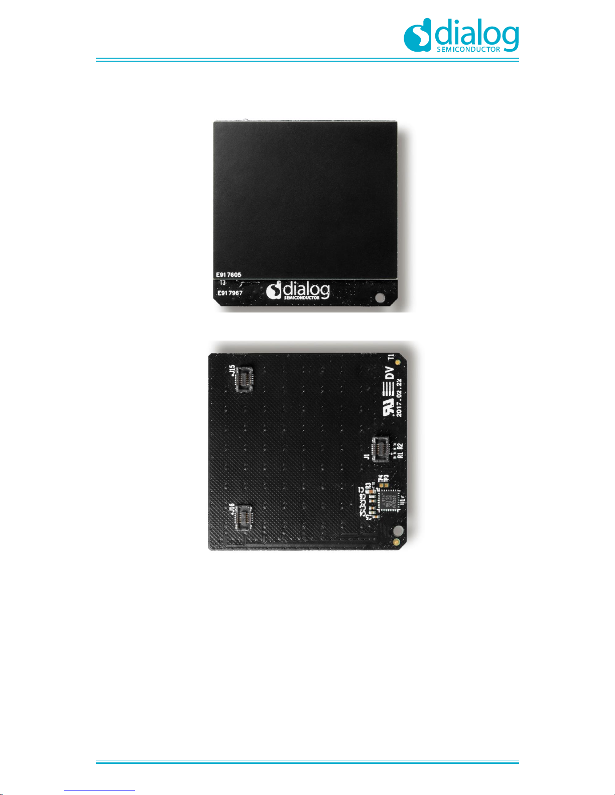
Figure 4: Trackpad Daughterboard (Rev B) – Top View
Figure 5: Trackpad Daughterboard (Rev B) – Bottom View
Page 8
UM-B-087
DA14585 Voice RCU Hardware Manual
User Manual
Revision 1.0
09-Jun-2017
CFR0012
8 of 34
© 2017 Dialog Semiconductor
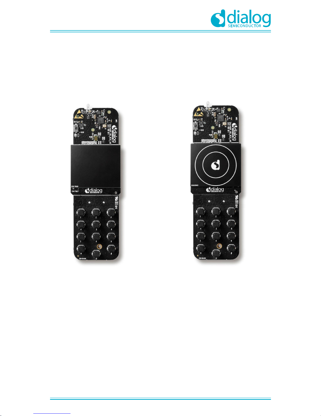
Figure 7: Complete DA14585
Voice RCU Reference Design
(Rev B) with Trackpad
Figure 6: Complete DA14585
Voice RCU Reference Design
(Rev B) with Track Wheel
Page 9
UM-B-087
DA14585 Voice RCU Hardware Manual
User Manual
Revision 1.0
09-Jun-2017
CFR0012
9 of 34
© 2017 Dialog Semiconductor
5 DA14585 Voice RCU Reference Design
5.1 DA14585 SoC
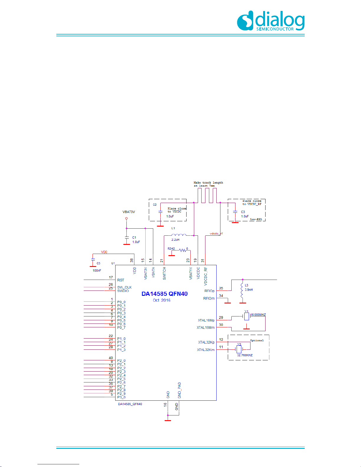
The DA14585 integrated circuit is an optimized version of the DA14580, offering a reduced boot time
and supporting up to eight connections. It has a fully integrated radio transceiver and baseband
processor for Bluetooth® low energy. It can be used as a standalone application processor or as a
data pump in hosted systems.
The device is optimized for remote control units (RCU) requiring support for voice commands and
motion/gesture recognition. Its integrated Audio Unit (AU) offers an easy interface for MEMS
microphones over PDM, external codecs over PCM/I2S and a Sample Rate Converter unit.
The Bluetooth Low Energy firmware includes the L2CAP service layer protocols, Security Manager
(SM), Attribute Protocol (ATT), the Generic Attribute Profile (GATT) and the Generic Access Profile
(GAP). All profiles published by the Bluetooth SIG as well as custom profiles are supported.
The transceiver interfaces directly to the antenna and is fully compliant with the Bluetooth 5.0
standard. The DA14585 has dedicated hardware for the Link Layer implementation of Bluetooth low
energy and interface controllers for enhanced connectivity capabilities.
Figure 8: DA14585 System Schematic
Page 10
UM-B-087
DA14585 Voice RCU Hardware Manual
User Manual
Revision 1.0
09-Jun-2017
CFR0012
10 of 34
© 2017 Dialog Semiconductor
5.2 Pin Assignment
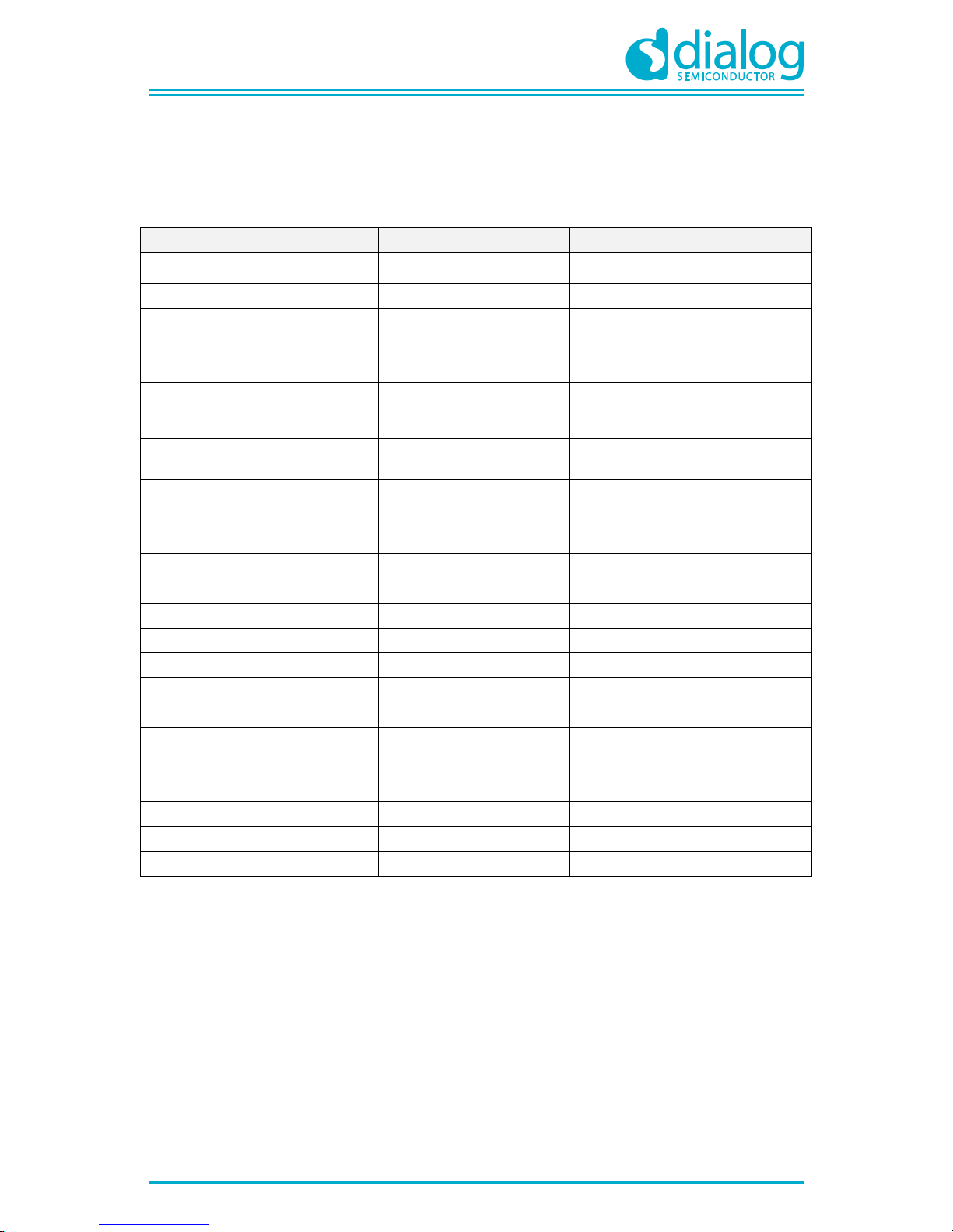
Table 1 shows the pin assignment and related pin names on the QFN40 package of the DA14585.
Table 1: DA14585 Voice RCU Reference Design Rev. B - Pin Assignment
DA14585 QFN40 Pin Name
Reference Design Signal
Section
P0_0
SPI_CLK
SPI clock (Flash memory)
P0_1
COL_2
Keypad
P0_2
COL_3
Keypad
P0_3
SPI_CS
SPI chip select (Flash memory)
P0_4
UTX
UART transmit signal
P0_5
URX /
SPI_MISO
UART receive signal /
SPI data in (Flash memory
and accelerometer/gyro)
P0_6
SPI_MOSI
SPI data out (Flash memory
and accelerometer/gyro)
P0_7
BUZ_EN
Enables buzzer
P1_0
PDM_DATA
Audio interface (Mic)
P1_1
PDM_CLK
Audio interface (Mic)
P1_2
Red LED
Programming LED indication
P1_3
Green LED
Keypad/trackpad operation indication
P2_0
IR LED
IR LED
P2_1
ROW_1
Keypad
P2_2
ROW_1
Keypad
P2_3
ROW_1
Keypad
P2_4
ROW_1
Keypad
P2_5
SDA
I2C data (Touch pad controller)
P2_6
SCK
I2C clock (Touch pad controller)
P2_7
RDY
Data ready (Touch pad controller)
P2_8
COL_1
Keypad
P2_9
SPI_CS1
Accelerometer/gyro chip select
P3_0
INT1_BMI
Accelerometer/gyro interrupt pin
Page 11
UM-B-087
DA14585 Voice RCU Hardware Manual
User Manual
Revision 1.0
09-Jun-2017
CFR0012
11 of 34
© 2017 Dialog Semiconductor
5.3 Power Management
The DA14585 SoC power management subsystem consists of:
● VBAT1V: INPUT. Battery connection. Used for an Alkaline or a NiMh battery (1.5 V). Power input
in boost configuration only. For buck configuration, this pin is shorted to GND.
● VBAT3V: INPUT/OUTPUT. Battery connection for a single coin battery (3 V) or dual AAA
batteries (2x 1.5 V). Power input in buck configuration only.
● SWITCH: INPUT/OUTPUT. Connection for the external inductor of the DC-DC converter.
● VDCDC: Output of the DC-DC converter.
● VDCDC_RF: Supply input of the Bluetooth radio.
● VDD: INPUT. This pin is used for testing purposes only.
Power supply of the DA14585 Voice RCU reference design:
● Battery type: Two standard AAA batteries (non-rechargeable).
● DC-DC converter: The internal DC-DC converter has been configured to operate in Buck mode.
● Power ON/OFF switch: This reference design is equipped with a power ON/OFF switch.
● VDCDC – VDCDC_RF track length: The PCB track between the VDCDC_RF and VDCDC pins
should be at least 7 mm long.
5.4 Flash Memory
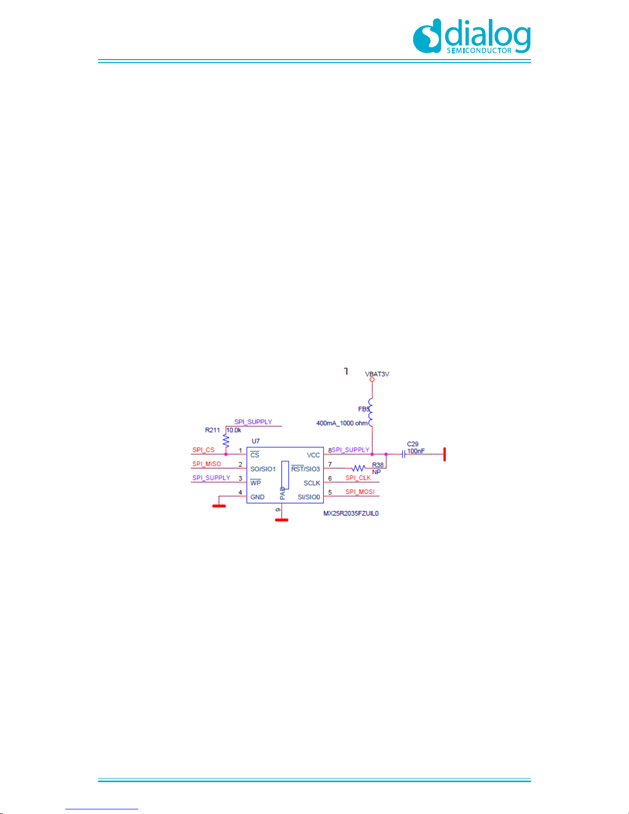
Figure 9: Serial NOR Flash Memory
The DA14585 uses an external Serial NOR Flash memory for mirroring its contents to RAM and
execute. The Flash memory type used is MX25R2035:
● 2 Mbit QSPI Flash memory, operated in single I/O mode
● Operating voltage: 1.65 V to 3.6 V for read, erase and program operations
Please notice that a pull-up resistor was added on the chip select pin. The reason is that during
power-up and power-down, pin CS# needs to follow the voltage applied to pin VCC to keep the
device not selected.
Page 12
UM-B-087
DA14585 Voice RCU Hardware Manual
User Manual
Revision 1.0
09-Jun-2017
CFR0012
12 of 34
© 2017 Dialog Semiconductor
5.5 Crystal Oscillators
The DA14585 SoC has two Digitally Controlled Crystal Oscillators (DCXO), one at 16 MHz
(XTAL16M) and a second at 32.768 kHz (XTAL32K). The 32.768 kHz oscillator has no trimming
capabilities and is used as the clock for the Extended/Deep Sleep modes. The 16 MHz oscillator can
be trimmed.
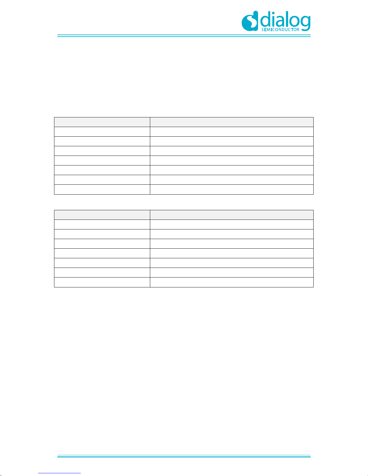
The crystals used on the DA14585 Voice RCU reference design are specified in Table 2 and Table 3.
Table 2: Y1 (16 MHz Crystal) Characteristics
Reference Designator
Value
Part Number
7M-16.000MEEQ-T
Frequency
16 MHz
Accuracy
±10 ppm
Load Capacitance (CL)
10 pF
Shunt Capacitance (C0)
3 pF
Equivalent Series Resistance (ESR)
100 Ω
Drive Level (PD)
50 W
Table 3: Y2 (32 kHz Crystal) Characteristics
Reference Designator
Value
Part Number
ABS07-120-32.768KHZ-T
Frequency
32.768 kHz
Accuracy
±20 ppm
Load Capacitance (CL)
6 pF
Shunt Capacitance (C0)
1.2 pF
Equivalent Series Resistance (ESR)
55-60 kΩ
Drive Level (PD)
0.1 to 0.5 W
Page 13
UM-B-087
DA14585 Voice RCU Hardware Manual
User Manual
Revision 1.0
09-Jun-2017
CFR0012
13 of 34
© 2017 Dialog Semiconductor
5.6 Microphone
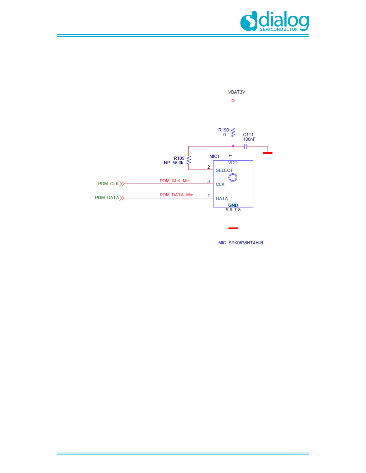
The SPK0838HT4H-B from Knowles is a miniature, high performance, low power, top port silicon
digital microphone with a single-bit PDM output. Its power consumption during sleep is only 4.6 A.
Figure 10: SPK0838HT4H Microphone Schematic
Page 14
UM-B-087
DA14585 Voice RCU Hardware Manual
User Manual
Revision 1.0
09-Jun-2017
CFR0012
14 of 34
© 2017 Dialog Semiconductor
5.7 Capacitive Touch Controller
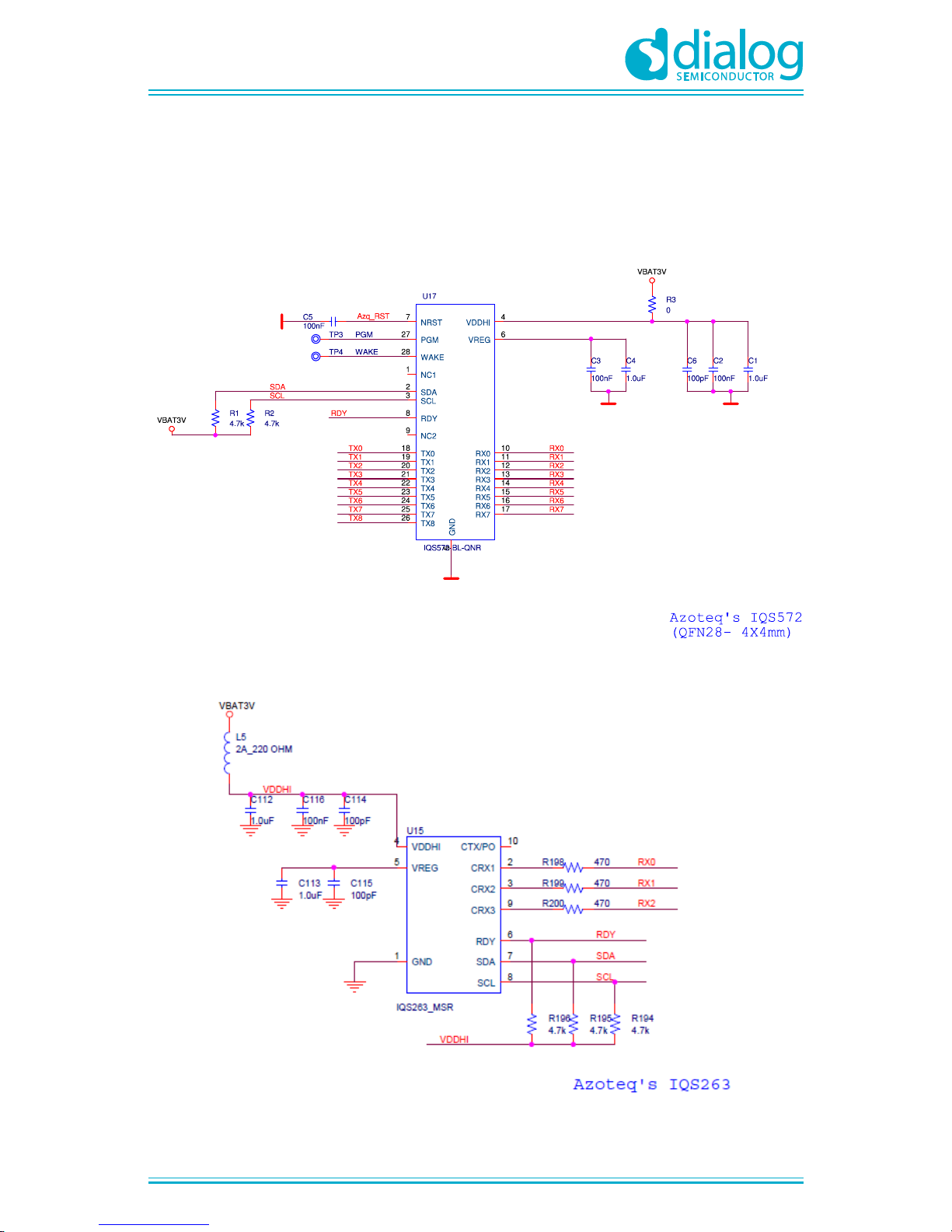
The trackpad of the DA14585 voice RCU reference design is equipped with a capacitive touch and
proximity controller IQS572 from Azoteq while the wheel pad is using the IQS263 from same vendor.
These controllers have the ability to sense touch and are accessible by the DA14585 via the I2C
interface.
Figure 11: Capacitive Touch Controller Schematic (Trackpad)
Figure 12: Capacitive Touch Controller Schematic (Wheel)
Page 15
UM-B-087
DA14585 Voice RCU Hardware Manual
User Manual
Revision 1.0
09-Jun-2017
CFR0012
15 of 34
© 2017 Dialog Semiconductor
5.8 Accelerometer/Gyroscope Sensor
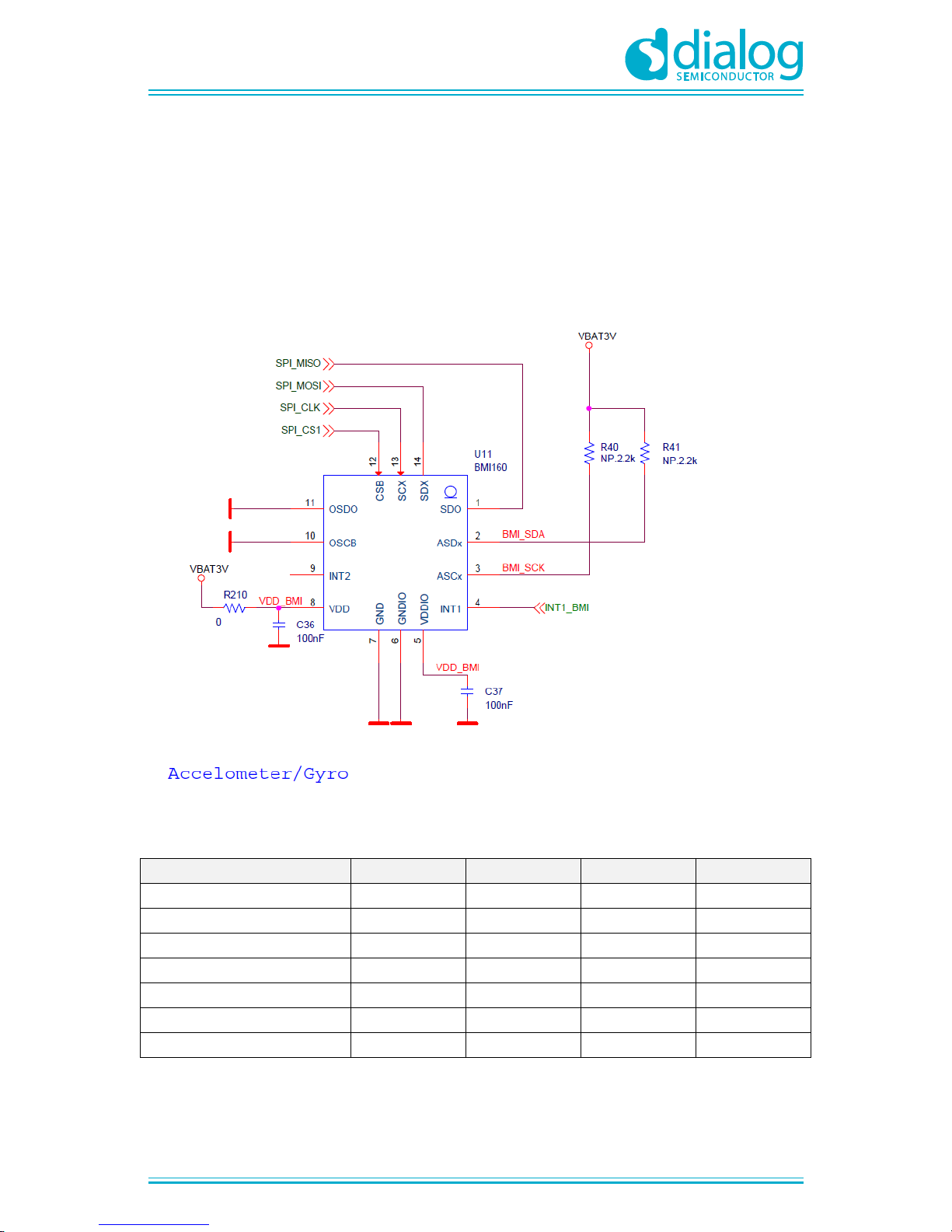
The DA14585 Voice RCU reference design includes the BMI160 Combined Inertial Measurement
Unit and Accelerometer sensor module from Bosch SensorTec.
The BMI160 is a low-power, low-noise inertial measurement unit, designed for use in mobile and
indoor applications which require highly accurate, real-time sensor data. In full operation mode, with
the accelerometer and gyroscope enabled, the current consumption is typically 950 A, while this is
dropped down to 3 A is suspend mode. The BMI160 module is connected to the DA14585 via an
SPI interface.
Figure 13: BMI160- Inertial Sensor Schematic
Table 4: BMI160 Inertial Sensor - Electrical Characteristics
Parameter
Min
Typ
Max
Unit
Supply Voltage (VDD)
1.71
3.0
3.6
V
Supply Voltage (VDD I/O)
1.2
2.4
3.6
V
Voltage Input Low Level
0.3*VDD I/O
V
Voltage Input High Level
0.7*VDD I/O
V
Voltage Output Low Level
0.2*VDD I/O
V
Voltage Output High Level
0.23*VDD I/O
V
Operating Temperature
-40 85
°C
Page 16
UM-B-087
DA14585 Voice RCU Hardware Manual
User Manual
Revision 1.0
09-Jun-2017
CFR0012
16 of 34
© 2017 Dialog Semiconductor
5.9 Infrared LED
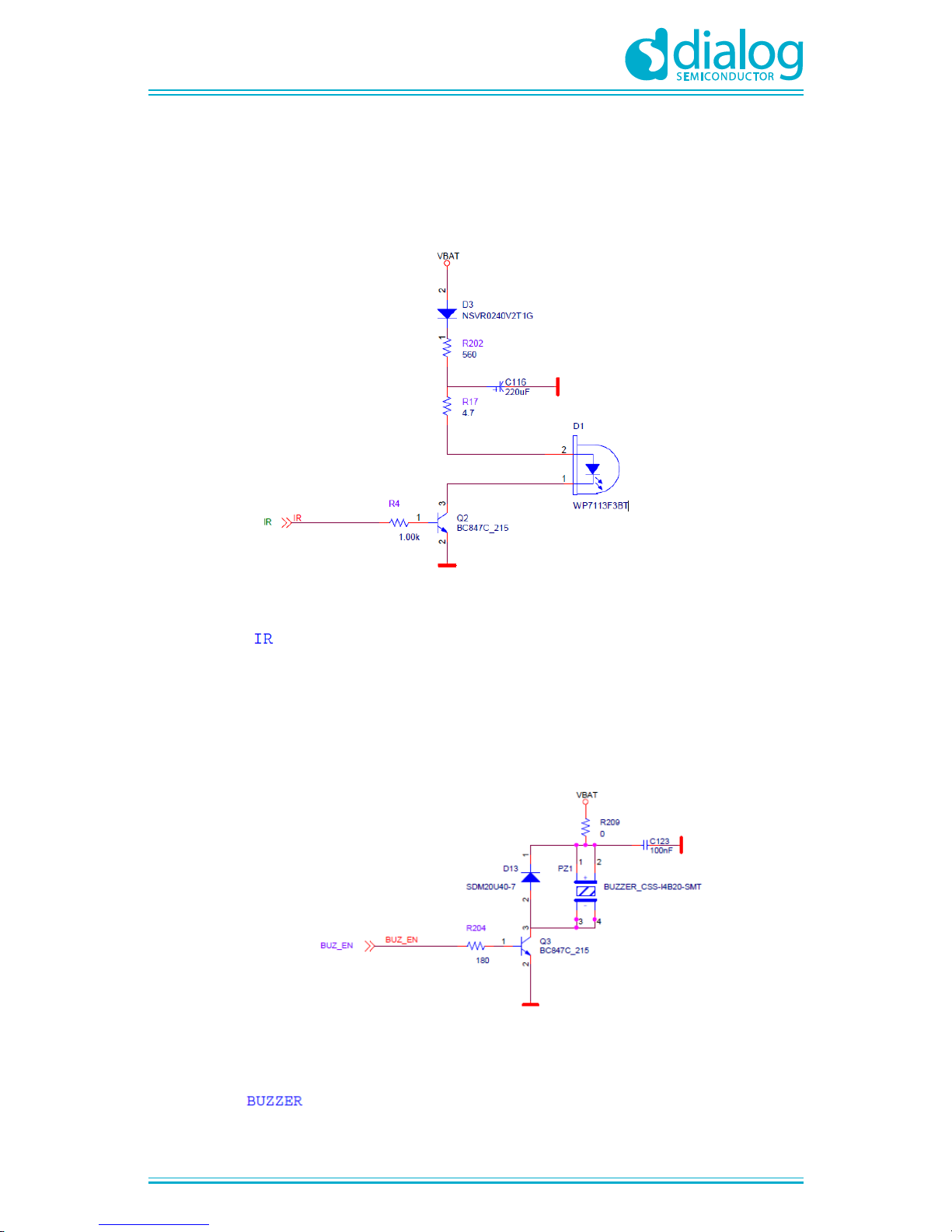
The DA14585 voice RCU reference design employs the WP7113F3BT IR LED from Kingbright.
A Schottky diode NSVR0240V2T1G is used to ensure that no current will be reflected back to
battery. The IR LED is driven by the P2_0 GPIO via a transistor switch.
Figure 14: IR LED Schematic
5.10 Buzzer
The DA14585 Voice RCU reference design employs the CSS-I4B20-SMT magnetic buzzer
transducer from CUI INC. The buzzer is driven by the P0_7 GPIO via a transistor switch.
Figure 15: Buzzer Schematic
Page 17
UM-B-087
DA14585 Voice RCU Hardware Manual
User Manual
Revision 1.0
09-Jun-2017
CFR0012
17 of 34
© 2017 Dialog Semiconductor
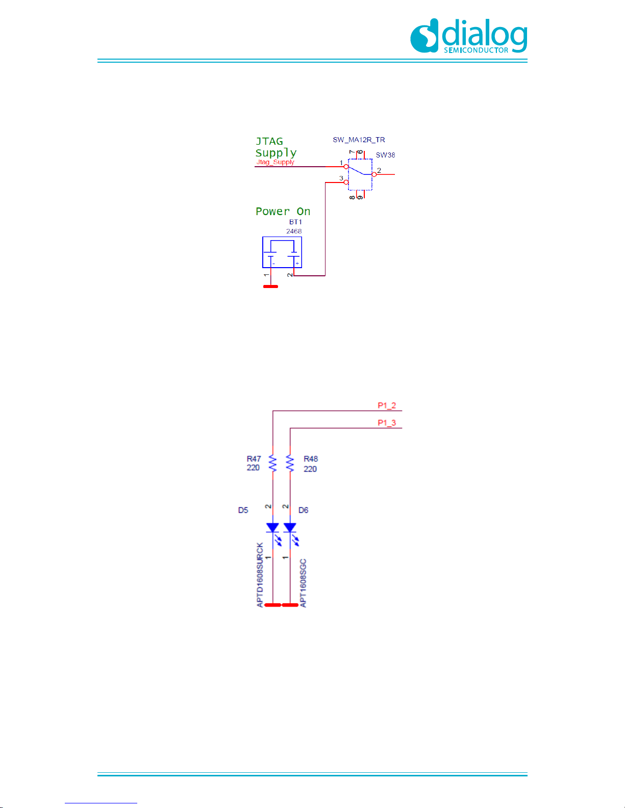
5.11 ON/OFF Switch
Figure 16: Power ON/OFF Switch Schematic
The DA14585 Voice RCU reference design is equipped with a two-position ON/OFF switch, which
selects the system to be powered by the battery or via the JTAG supply.
5.12 LEDs
Figure 17: Indication LEDs Schematic
The DA14585 Voice RCU reference design is equipped with a Red LED (D5) and a Green LED (D6),
which are used to indicate programming and keypad/trackpad operations, respectively. The Red LED
is controlled by GPIO P1_2, the Green LED by GPIO P1_3.
Page 18
UM-B-087
DA14585 Voice RCU Hardware Manual
User Manual
Revision 1.0
09-Jun-2017
CFR0012
18 of 34
© 2017 Dialog Semiconductor
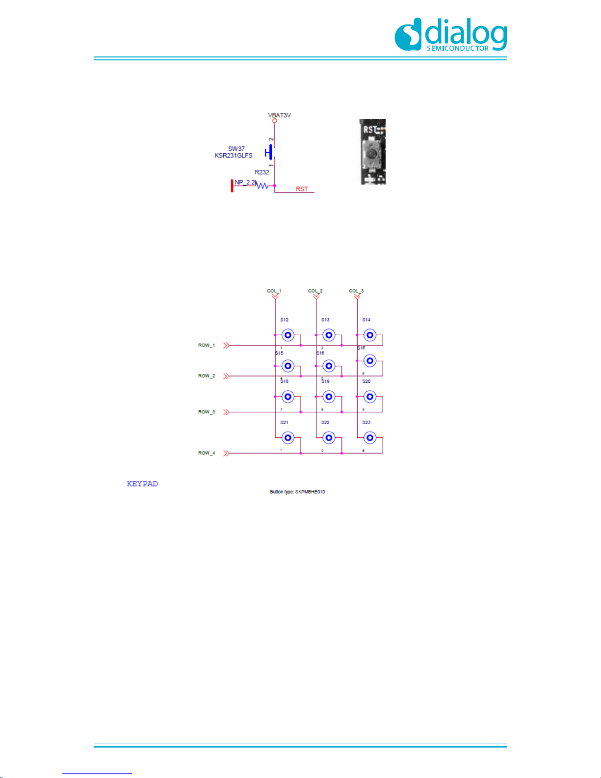
5.13 Reset Button
Figure 18: Reset Button Schematic and Actual Illustration
The DA14585 Voice RCU reference design employs a reset button (SW37) for applying a hard reset
of the DA14585 SoC.
5.14 Keypad Matrix
Figure 19: Keypad Matrix Schematic
The DA14585 Voice RCU reference design uses a fully configurable 3 columns by 4 rows keypad
matrix.
Page 19
UM-B-087
DA14585 Voice RCU Hardware Manual
User Manual
Revision 1.0
09-Jun-2017
CFR0012
19 of 34
© 2017 Dialog Semiconductor
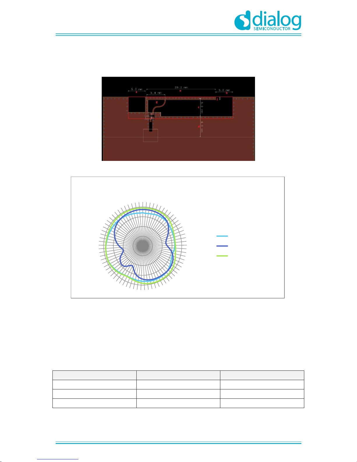
5.15 Printed Antenna
Figure 20: PCB view of a printed antenna
Figure 21: Printed Antenna Radiation Pattern
Printed antennas are low cost, easy to manufacture and provide diversity in polarization.
The antennas used in this reference design was based on the Designing Printed Antennas for
Bluetooth® Low Energy application note.
Figure 21 shows the radiation pattern of the printed IFA antenna used in the DA14585 Voice RCU
reference design. The antenna performance is summarized in Table 5.
Table 5: Printed Antenna Performance Characteristics
Parameter
Vertical Polarization
Horizontal Polarization
Peak Power [dBm]
-1.617
-2.565
Average EIRP [dBm]
-4.34000333
-6.24978
Total Radiated Power [dBm]
-2.18045194
-1.9
-40
-30
-20
-10
0
0
0
0
0
0
0
0
0
0
0
0
0
0
0
0
0
0
0
0
0
0
0
0
0
0
0
0
0
0
0
0
0
0
0
0
0
00
0
0
0
0
0
0
0
0
0
0
0
0
0
0
0
0
0
0
0
0
0
0
0
0
0
0
0
0
0
0
0
0
0
0
0
Standing [dBm]
vertical polarization
horizontal polarization
total
Page 20
UM-B-087
DA14585 Voice RCU Hardware Manual
User Manual
Revision 1.0
09-Jun-2017
CFR0012
20 of 34
© 2017 Dialog Semiconductor
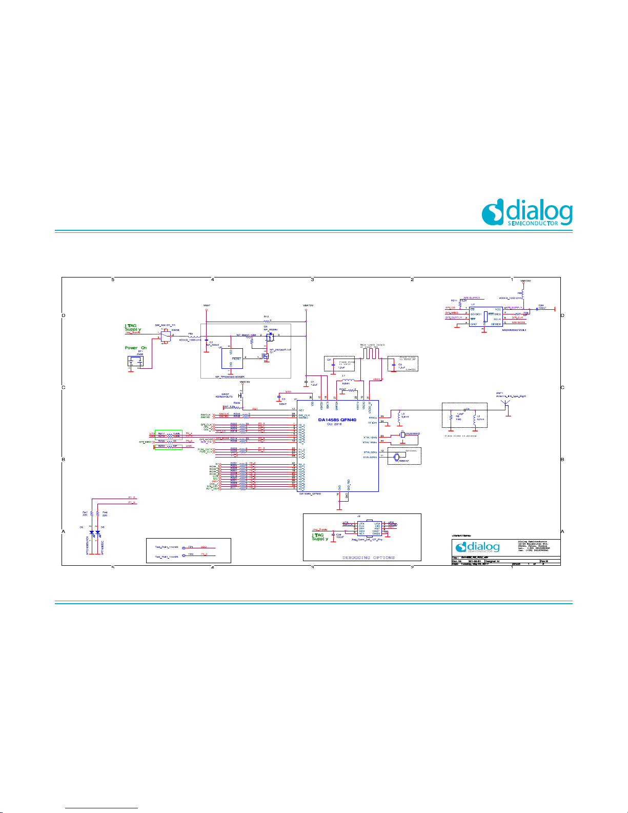
6 Schematics
Figure 22: DA14585 Voice RCU Reference Design Rev. B1 - SoC, Flash Memory, Debugging Port
Page 21
UM-B-087
DA14585 Voice RCU Hardware Manual
User Manual
Revision 1.0
09-Jun-2017
CFR0012
21 of 34
© 2017 Dialog Semiconductor
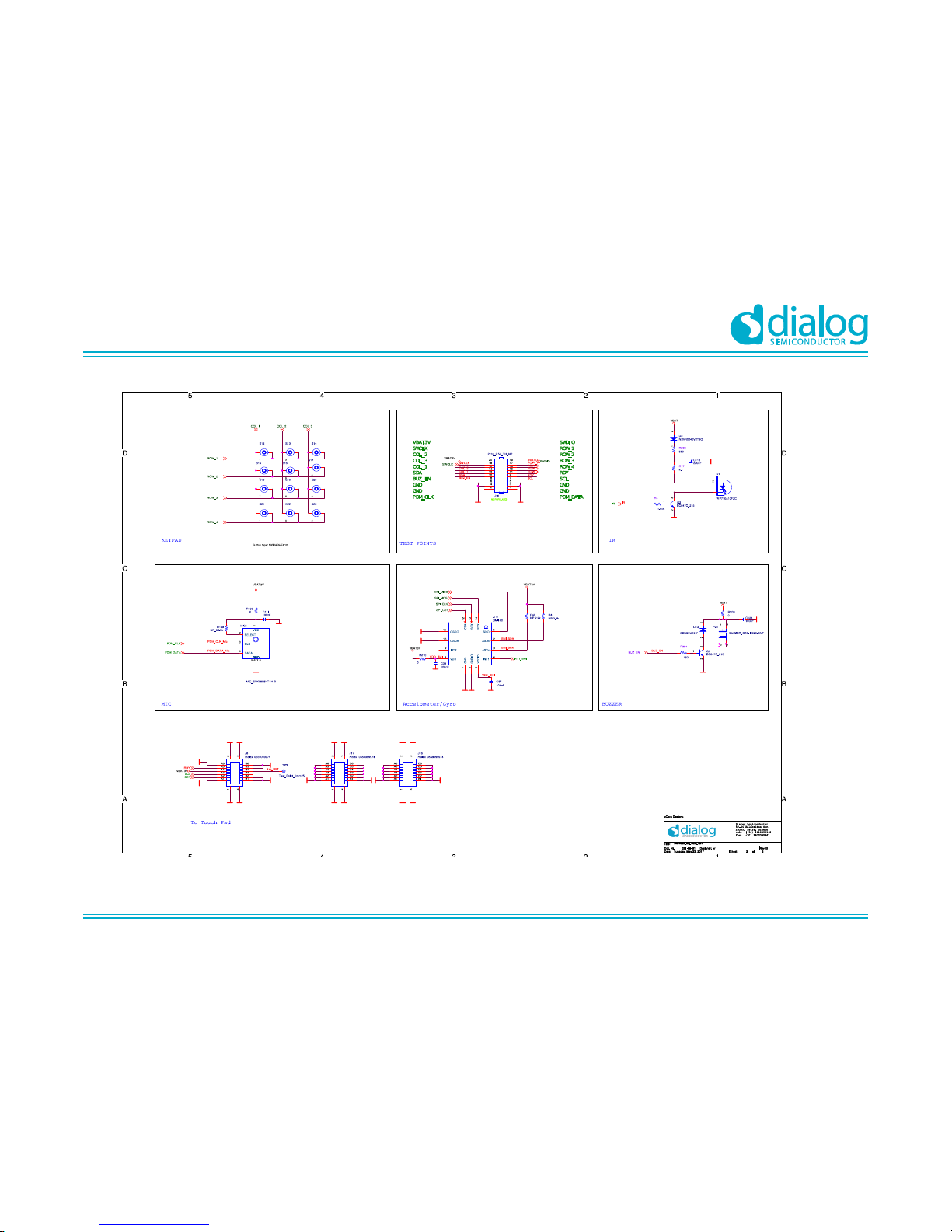
Figure 23: DA14585 Voice RCU Reference Design Rev. B1 – Peripherals, Sensors
Page 22
UM-B-087
DA14585 Voice RCU Hardware Manual
User Manual
Revision 1.0
09-Jun-2017
CFR0012
22 of 34
© 2017 Dialog Semiconductor
7 PCB Layout
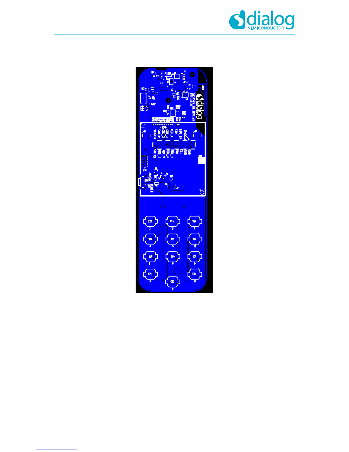
Figure 24: DA14585 Voice RCU Reference Design Rev. B - Top View
Page 23
UM-B-087
DA14585 Voice RCU Hardware Manual
User Manual
Revision 1.0
09-Jun-2017
CFR0012
23 of 34
© 2017 Dialog Semiconductor
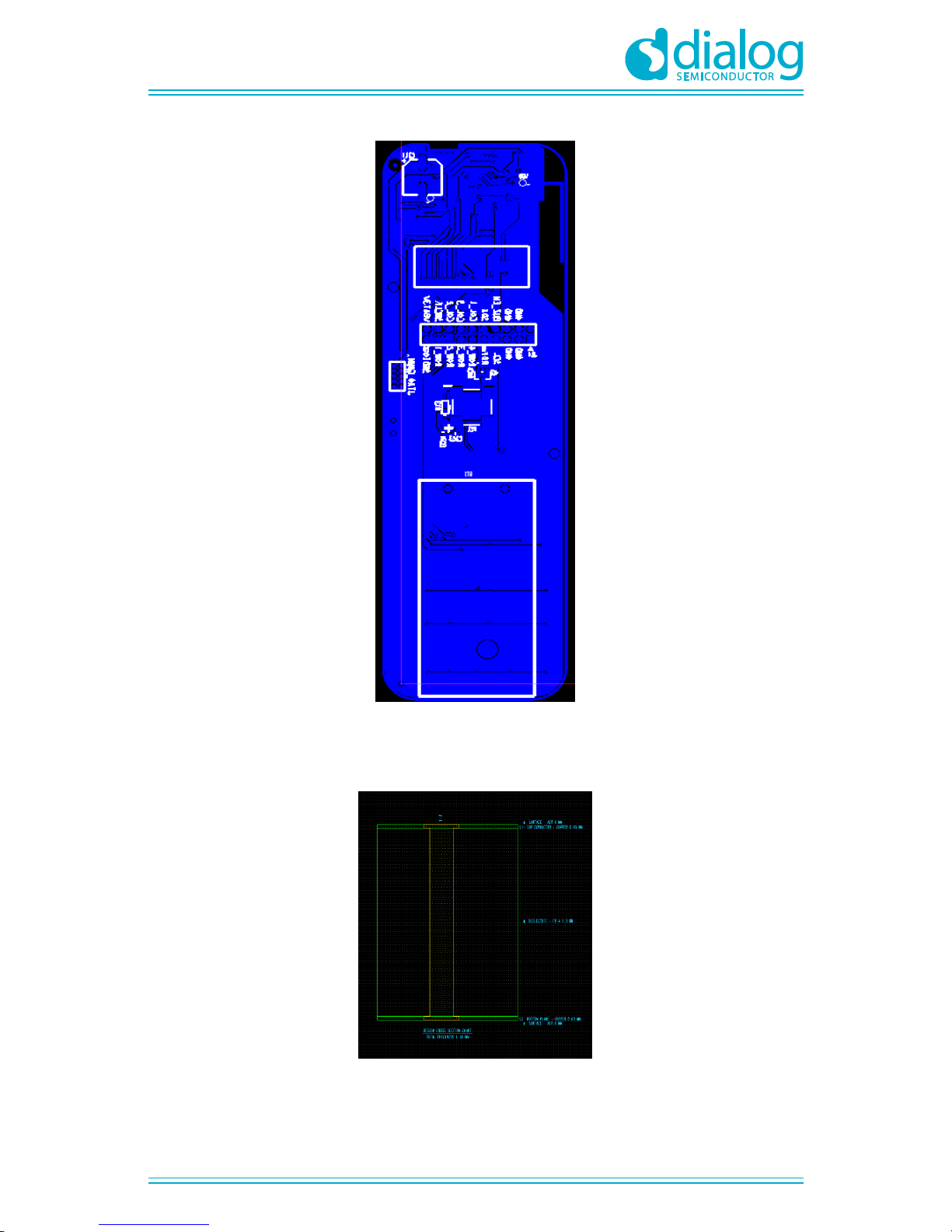
Figure 25: DA14585 Voice RCU Reference Design Rev. B - Bottom View
This is a 2-layer FR-4 PCB with approx. 1.6 mm thickness as can be seen from the stack-up figure
below:
Figure 26: DA14585 Voice RCU Reference Design - PCB Stack-Up
Page 24
UM-B-087
DA14585 Voice RCU Hardware Manual
User Manual
Revision 1.0
09-Jun-2017
CFR0012
24 of 34
© 2017 Dialog Semiconductor
8 Power Measurements
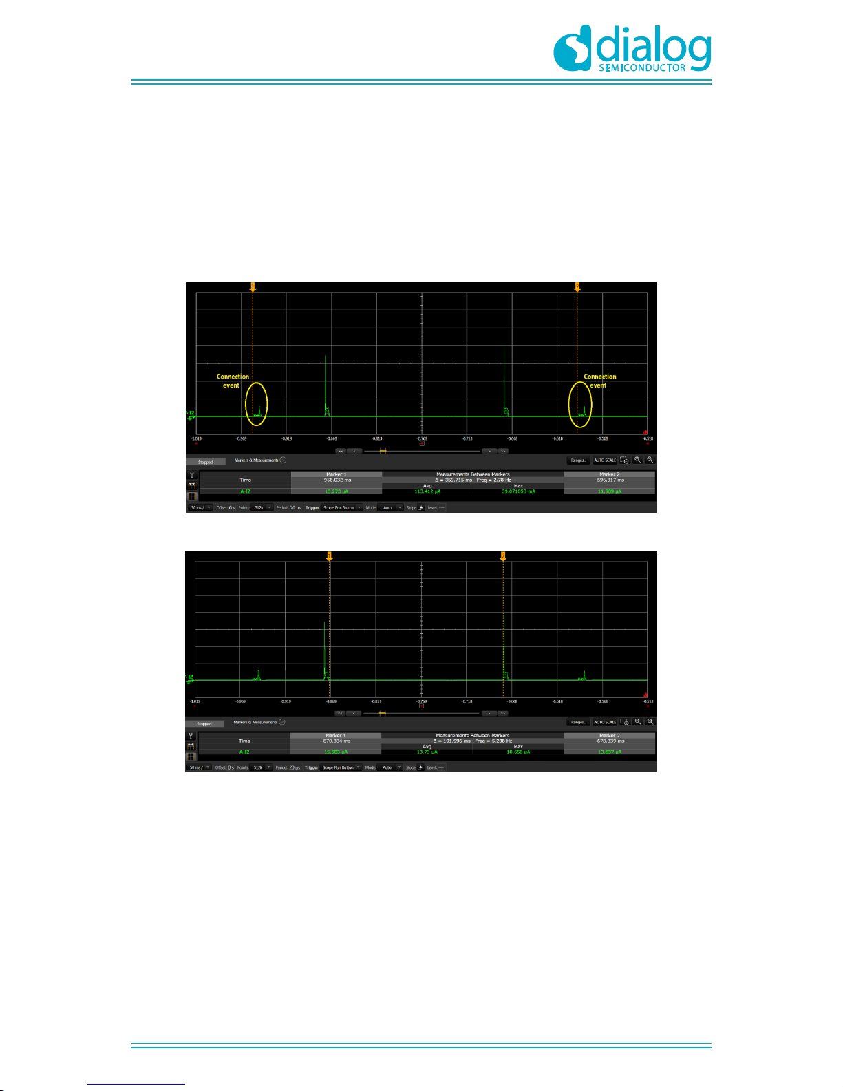
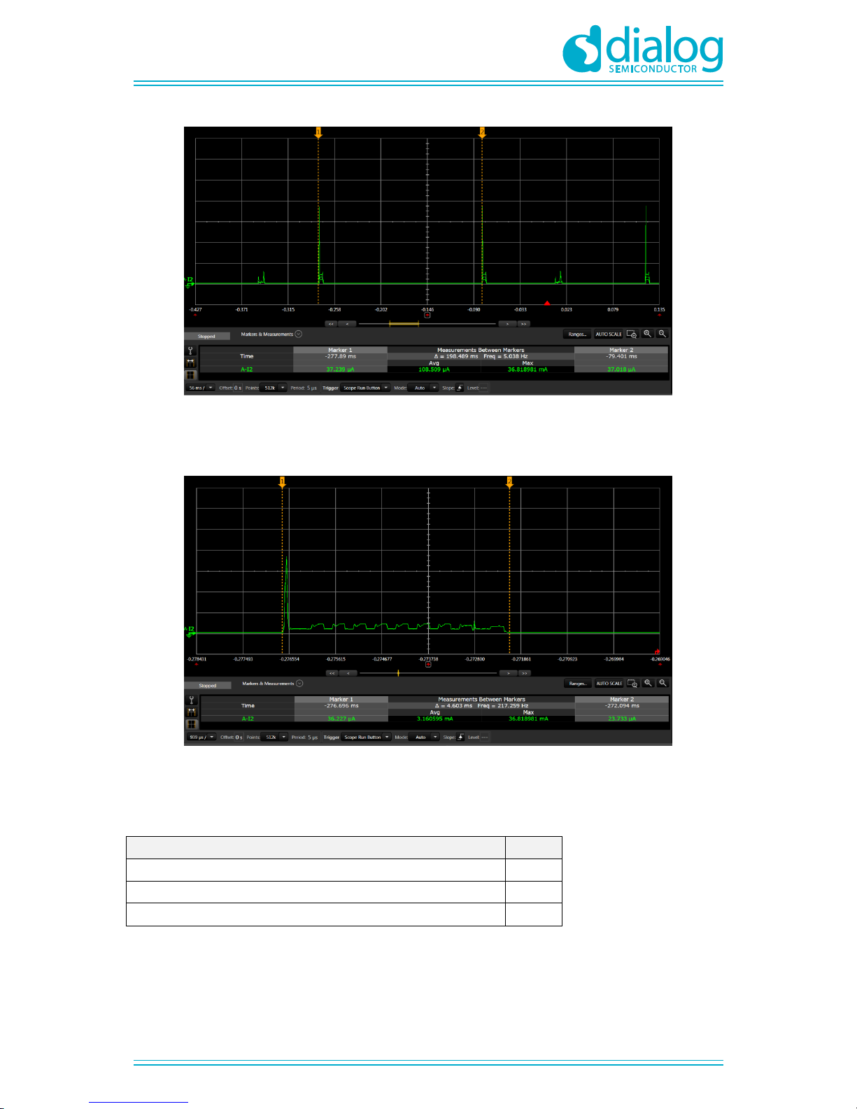
This chapter contains current consumption measurement results for the DA14585 Voice RCU
Reference Design. These measurements were conducted using the Agilent DC power analyzer
N6705B with the reference design connected to a mobile phone application.
Figure 27: DA14585 Voice RCU Reference Design – Average Operating Current
Figure 28: DA14585 Voice RCU Reference Design – Average Sleep Current
Page 25
UM-B-087
DA14585 Voice RCU Hardware Manual
User Manual
Revision 1.0
09-Jun-2017
CFR0012
25 of 34
© 2017 Dialog Semiconductor
Figure 29: DA14585 Voice RCU Reference Design – Average Touch Pad Scanning Current
Figure 29 shows the average current consumption of the DA14585 Voice RCU reference design,
emphasizing the scanning pulse generated by the touch pad controller.
Figure 30: DA14585 Voice RCU Reference Design – Current during Touch Pad Scan Pulse
Table 6: DA14585 Voice RCU Reference Design
Current consumption type
Value
Average Operating Current consumption (uA) - Normal mode
113.412
Average Operating Current consumption (uA) - Sleep mode
13.73
Average Operating Current consumption (uA) - Touch scanning event
108.509
Page 26
UM-B-087
DA14585 Voice RCU Hardware Manual
User Manual
Revision 1.0
09-Jun-2017
CFR0012
26 of 34
© 2017 Dialog Semiconductor
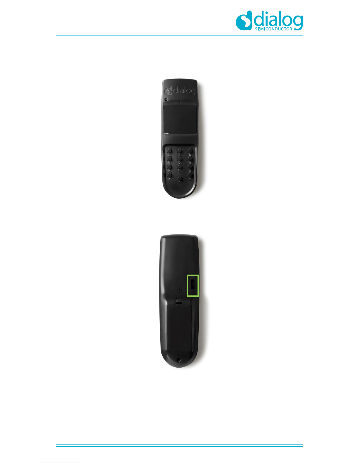
9 Enclosure
Figure 31: DA14585 Voice RCU Reference Design Enclosure – Top View
Figure 32: DA14585 Voice RCU Reference Design Enclosure – Bottom View
Debugging
port
Page 27
UM-B-087
DA14585 Voice RCU Hardware Manual
User Manual
Revision 1.0
09-Jun-2017
CFR0012
27 of 34
© 2017 Dialog Semiconductor
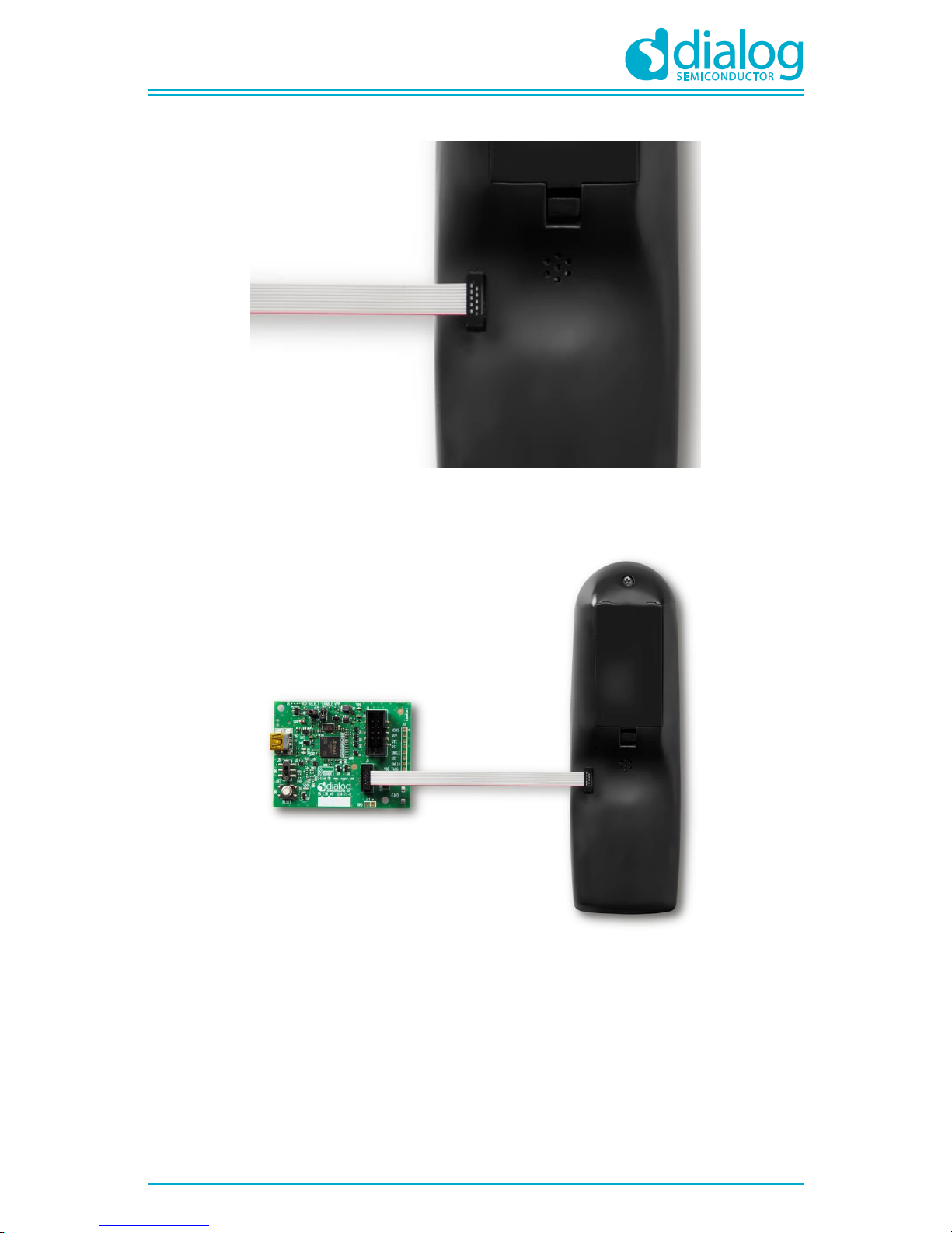
Figure 33: Connection of JTAG Cable with DA14585 Voice RCU PCB Inside Enclosure
Figure 34: Connection of CIB Board with DA14585 Voice RCU PCB inside the Enclosure
Page 28
UM-B-087
DA14585 Voice RCU Hardware Manual
User Manual
Revision 1.0
09-Jun-2017
CFR0012
28 of 34
© 2017 Dialog Semiconductor
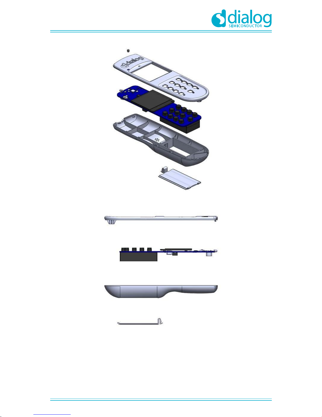
Figure 35: DA14585 Voice RCU Reference Design Enclosure – Top Exploded View
Figure 36 : DA14585 Voice RCU Reference Design Enclosure - Side Exploded View
Page 29
UM-B-087
DA14585 Voice RCU Hardware Manual
User Manual
Revision 1.0
09-Jun-2017
CFR0012
29 of 34
© 2017 Dialog Semiconductor
10 Configuration of the Debugging Interface
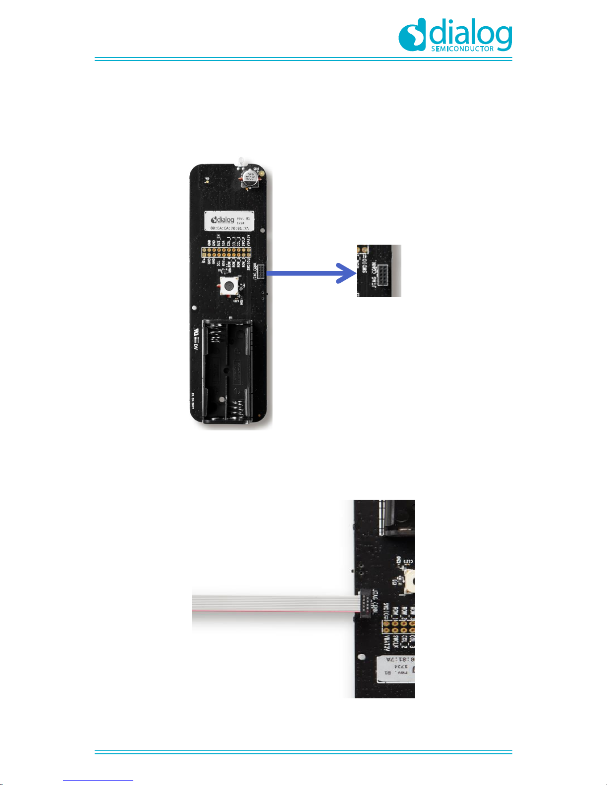
The DA14585 voice RCU reference design has a dedicated debugging port as shown in Figure 37 .
Two debugging ports are used on the DA14585 SoC: JTAG and UART.
Figure 37: Debug Interface
Figure 38 illustrates the proper way of connecting an IDC-10 programming/debugging cable coming
from the CIB programming board.
Figure 38: IDC-10 Programming/Debugging Cable Installation
Page 30
UM-B-087
DA14585 Voice RCU Hardware Manual
User Manual
Revision 1.0
09-Jun-2017
CFR0012
30 of 34
© 2017 Dialog Semiconductor
Debugging Using the CIB
The DA14585 Voice RCU reference design has a dedicated debugging port as shown in . Two
debugging ports are used on the DA14585 SoC: JTAG and UART.
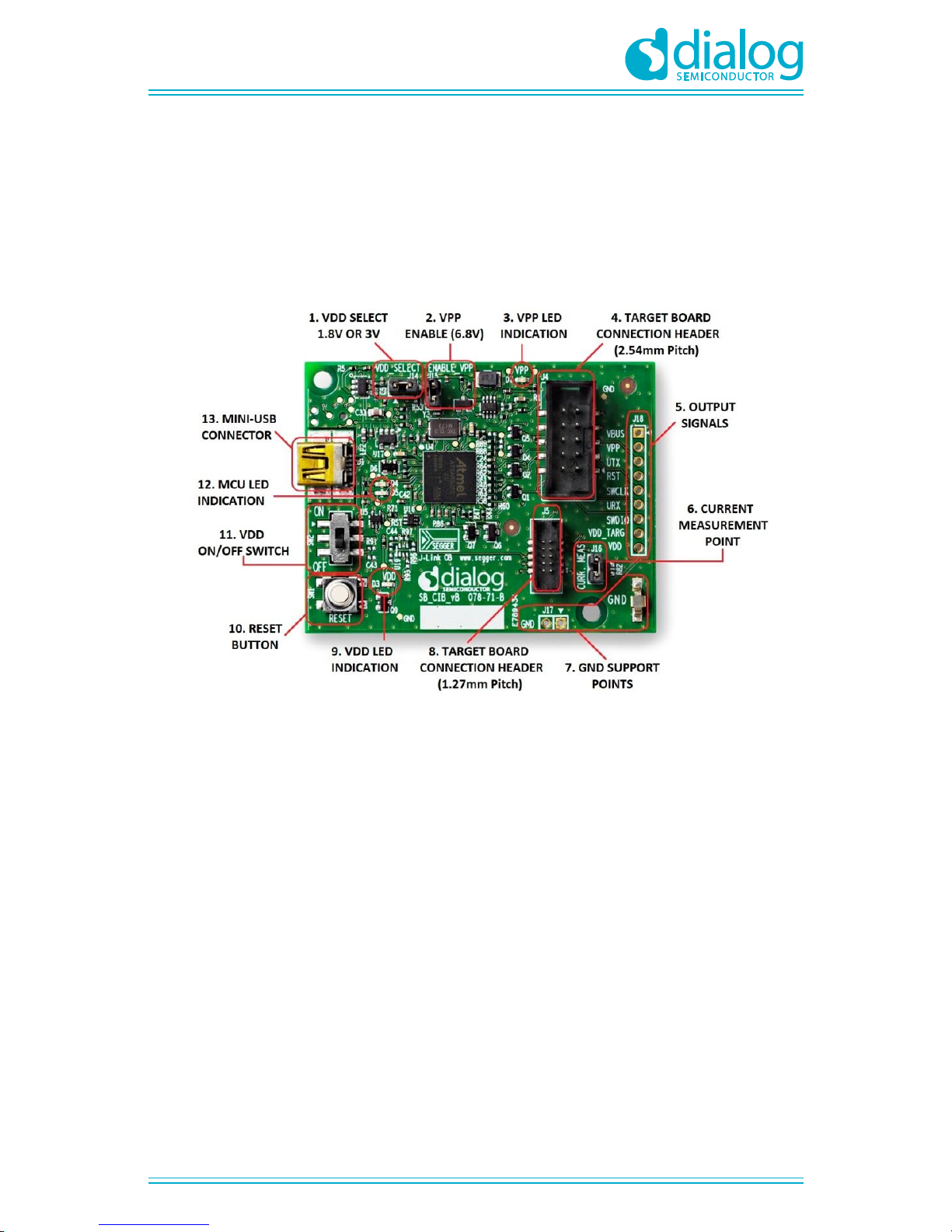
The USB-to-JTAG and USB-to-UART functions are implemented by an external Communication
Interface Board (CIB) as shown in Figure 39. This interface board has a SEGGER chip running the
JLink-OB firmware.
Figure 39: Communication Interface Board (CIB)
The following functions are performed by the interface board:
● Connectivity of PC to the DA14585 JTAG port
● Connectivity of PC to the DA14585 UART port (full UART is possible but it must be enabled on
the PC driver)
● Hardware RESET capability. Note that the RESET signal is active high.
The following on-board settings have to be enforced in order to be able to program /debug the
DA14585 voice RCU reference design board:
Interface board settings (see Figure 39):
● ON-OFF switch set to ON
● USB cable connected at the mini USB connector
● IDC-10 cable from the 1.27 mm pitch header to the target board
● IDC-10 cable from interface board is connected at the bottom of the voice RCU reference design
board
● ON-OFF switch has to be switched to ON position in order to be powered by the communication
interface board
● Jumper at J16 header should be populated
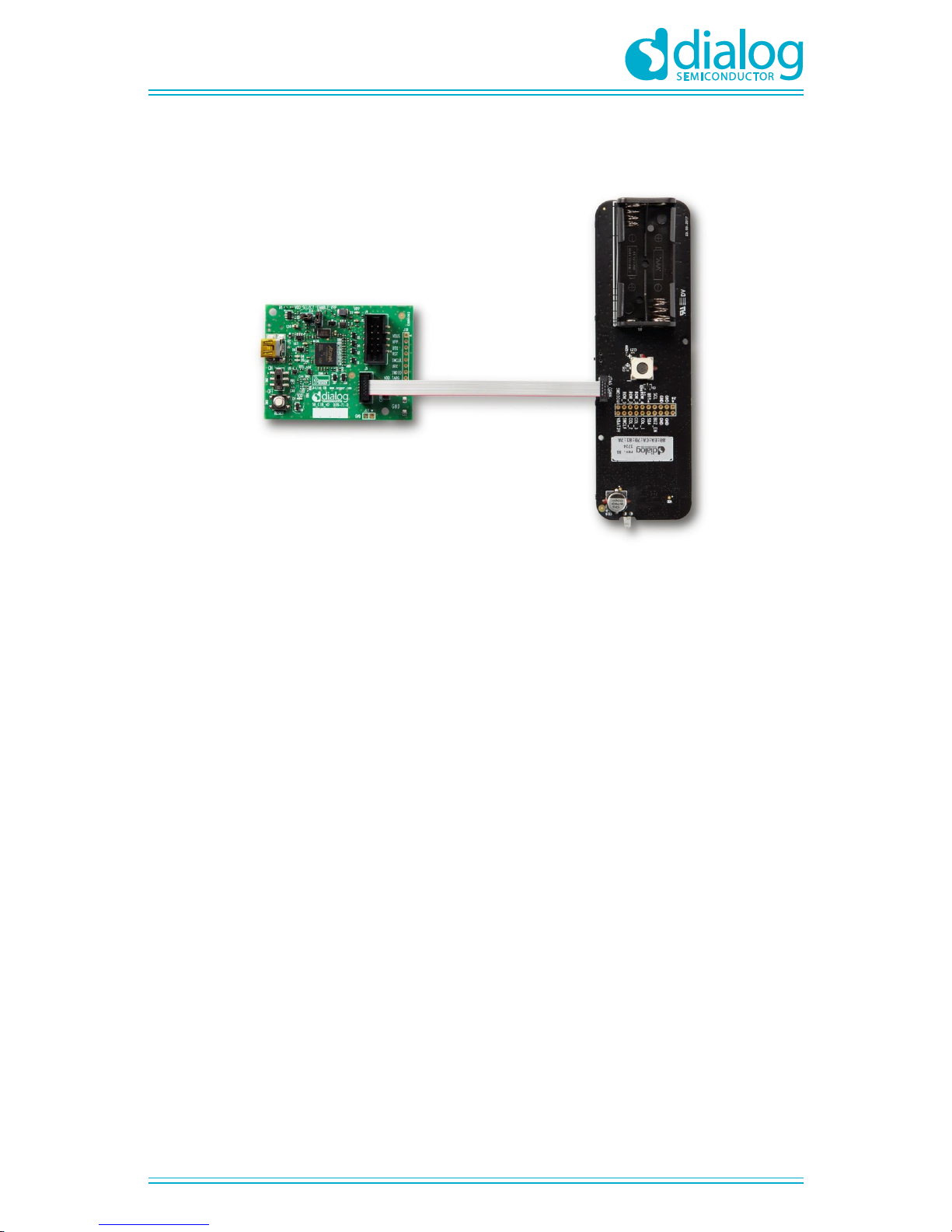
The connection between the interface board and the DA14585 voice RCU reference design board is
shown in Figure 40 .
Page 31
UM-B-087
DA14585 Voice RCU Hardware Manual
User Manual
Revision 1.0
09-Jun-2017
CFR0012
31 of 34
© 2017 Dialog Semiconductor
Figure 40: Connection of the DA14585 Voice RCU PCB to the CIB Programming Board
Page 32
UM-B-087
DA14585 Voice RCU Hardware Manual
User Manual
Revision 1.0
09-Jun-2017
CFR0012
32 of 34
© 2017 Dialog Semiconductor
10.1 Debug/Programming Interface Scenarios
The following two scenarios are targeted to help the user to successfully debug/program the
DA14585 Voice RCU reference design.
10.1.1 Scenario 1: RCU Inside the Enclosure
In this case the user must have the batteries installed before connecting the CIB programming/
debugging board, because the power ON/OFF switch is placed in ON position by default, prior to
shipping the reference design to the customer (see Figure 41). The debugging port of the enclosure
can be seen in Figure 32.
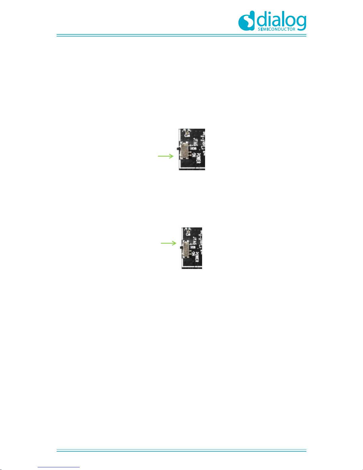
Figure 41: Power ON/OFF Switch Position for Scenario 1 (Green Arrow: ON)
10.1.2 Scenario 2: RCU Outside the Enclosure
In this case the user must either have the batteries installed before connecting the CIB programming/
debugging board or (when there are no batteries available) the reference design must be powered by
the CIB interface board, hence the power ON/OFF switch must be placed in the JTAG position (see
Figure 42).
Figure 42: Power ON/OFF Switch Position for Scenario 2 (Green Arrow: JTAG)
Page 33
UM-B-087
DA14585 Voice RCU Hardware Manual
User Manual
Revision 1.0
09-Jun-2017
CFR0012
33 of 34
© 2017 Dialog Semiconductor
Revision History
Revision
Date
Description
1.0
09-Jun-2017
Initial version.
Page 34

UM-B-087
DA14585 Voice RCU Hardware Manual
User Manual
Revision 1.0
09-Jun-2017
CFR0012
34 of 34
© 2017 Dialog Semiconductor
Status Definitions
Status
Definition
DRAFT
The content of this document is under review and subject to formal approval, which may result in
modifications or additions.
APPROVED
or unmarked
The content of this document has been approved for publication.
Disclaimer
Information in this document is believed to be accurate and reliable. However, Dialog Semiconductor does not give any
representations or warranties, expressed or implied, as to the accuracy or completeness of such information. Dialog
Semiconductor furthermore takes no responsibility whatsoever for the content in this document if provided by any information
source outside of Dialog Semiconductor.
Dialog Semiconductor reserves the right to change without notice the information published in this document, including without
limitation the specification and the design of the related semiconductor products, software and applications.
Applications, software, and semiconductor products described in this document are for illustrative purposes only. Dialog
Semiconductor makes no representation or warranty that such applications, software and semiconductor products will be
suitable for the specified use without further testing or modification. Unless otherwise agreed in writing, such testing or
modification is the sole responsibility of the customer and Dialog Semiconductor excludes all liability in this respect.
Customer notes that nothing in this document may be construed as a license for customer to use the Dialog Semiconductor
products, software and applications referred to in this document. Such license must be separately sought by customer with
Dialog Semiconductor.
All use of Dialog Semiconductor products, software and applications referred to in this document are subject to Dialog
Semiconductor’s Standard Terms and Conditions of Sale, available on the company website (www.dialog-semiconductor.com)
unless otherwise stated.
Dialog and the Dialog logo are trademarks of Dialog Semiconductor plc or its subsidiaries. All other product or service names
are the property of their respective owners.
© 2017 Dialog Semiconductor. All rights reserved.
Contacting Dialog Semiconductor
United Kingdom (Headquarters)
Dialog Semiconductor (UK) LTD
Phone: +44 1793 757700
Germany
Dialog Semiconductor GmbH
Phone: +49 7021 805-0
The Netherlands
Dialog Semiconductor B.V.
Phone: +31 73 640 8822
North America
Dialog Semiconductor Inc.
Phone: +1 408 845 8500
Japan
Dialog Semiconductor K. K.
Phone: +81 3 5425 4567
Taiwan
Dialog Semiconductor Taiwan
Phone: +886 281 786 222
Singapore
Dialog Semiconductor Singapore
Phone: +65 64 8499 29
Hong Kong
Dialog Semiconductor Hong Kong
Phone: +852 3769 5200
Korea
Dialog Semiconductor Korea
Phone: +82 2 3469 8200
China (Shenzhen)
Dialog Semiconductor China
Phone: +86 755 2981 3669
China (Shanghai)
Dialog Semiconductor China
Phone: +86 21 5424 9058
Email:
Web site:
www.dialog-semiconductor.com
 Loading...