


User Manual
DA14531 Development Kit Pro
Hardware User Manual
UM-B-114
Abstract
Dialog Semiconductor’s DA14531 development kit PRO consists of one DA145xx DEVKT-P PROMotherboard, FCGQNFN daughterboard and a WLCSP daughterboard (the WLCSP daughterboard
must be purchased separately). This user manual describes the system functions of the hardware as
well as the guidelines of how to enable or disable features of the DA14531 development kit PRO.

UM-B-114
DA14531 Development Kit Pro Hardware User Manual
User Manual
Revision 1.1
25-Oct-2019
CFR0012
2 of 80
© 2019 Dialog Semiconductor
Contents
Abstract ................................................................................................................................................ 1
Contents ............................................................................................................................................... 2
Figures .................................................................................................................................................. 4
Tables ................................................................................................................................................... 5
1 Terms and Definitions ................................................................................................................... 7
2 References ..................................................................................................................................... 7
3 Introduction .................................................................................................................................... 8
3.1 System Overview ................................................................................................................ 10
3.1.1 Features of DA14531 PRO-DB ........................................................................... 10
3.1.2 Features of DA14531 PRO-MB ........................................................................... 10
4 Getting to Know DA14531 DK PRO ........................................................................................... 11
4.1 DA14531 PRO-DB .............................................................................................................. 11
4.1.1 Power Section ...................................................................................................... 13
4.1.2 RF Section ........................................................................................................... 15
4.2 PRO-MB (376-18-B) ............................................................................................................ 16
4.2.1 USB HUB (U11) ................................................................................................... 18
4.2.2 USB to UART (U12) ............................................................................................. 18
4.2.3 USB to JTAG (U4) ............................................................................................... 19
4.2.4 Voltage Translator ............................................................................................... 20
4.2.5 Power Section ...................................................................................................... 21
5 GPIOs and Pin Assignment and Functions of DA14531 DK PRO .......................................... 22
5.1 DA14531 WLCSP17 PRO-DB, Default Setup .................................................................... 24
5.2 DA14531 FCGQFN24 PRO-DB, Default Setup .................................................................. 25
5.3 PRO-MB Setup ................................................................................................................... 27
5.3.1 Reset.................................................................................................................... 27
5.3.2 JTAG .................................................................................................................... 28
5.3.3 SPI Data Flash (U2) ............................................................................................. 28
5.3.4 UART ................................................................................................................... 29
Single-wire UART ................................................................................................ 30
5.3.4.1 2-wire UART Configuration .............................................................. 30
5.3.4.2 Full UART (4-wire) Configuration .................................................... 31
5.3.5 Push Buttons ....................................................................................................... 32
5.3.6 User LED (D5) and C-Trig (Software Cursor) ..................................................... 33
5.3.7 mikroBUS 2 Interface ........................................................................................... 34
5.3.8 Arduino Interface ................................................................................................. 35
6 How to Configure Power of DA14531 DK PRO ......................................................................... 36
6.1 Battery Operation ................................................................................................................ 37
6.1.1 Enabling Coin Cell Battery on DA14531 PRO-DB .............................................. 38
6.1.2 Enabling Coin Cell Battery on PRO-MB .............................................................. 38
7 First Steps with DA14531 DK PRO ............................................................................................ 40
7.1 Configuration of DA14531 DK PRO with a DA14531 FCGQFN24 PRO-DB ...................... 40
7.2 Configuration of DA14531 DK PRO with a DA14531 WLCSP17 PRO-DB ........................ 42
8 Current Measurements ............................................................................................................... 43

UM-B-114
DA14531 Development Kit Pro Hardware User Manual
User Manual
Revision 1.1
25-Oct-2019
CFR0012
3 of 80
© 2019 Dialog Semiconductor
8.1 Current Measurement Circuit of PRO-MB .......................................................................... 43
8.2 Power Profiler of Smartsnippet Toolbox ............................................................................. 44
8.3 Power Profiler Setup ........................................................................................................... 45
8.4 Measurements .................................................................................................................... 47
8.5 Power Profiler Software Cursors ......................................................................................... 49
8.6 Manual Calibration .............................................................................................................. 49
8.7 Accuracy of Current Measurement Circuit .......................................................................... 51
9 Known Issues .............................................................................................................................. 53
9.1 Switching Transient Artifacts of Current Measurement Circuit ........................................... 53
9.2 Push Button SW3 ................................................................................................................ 53
9.3 mikroBUS Wrong Label ....................................................................................................... 54
9.4 4-Wire UART Special Considerations ................................................................................. 54
Appendix A FCGQFN24 PRO-DB: DA14531-00FXDB-P_(376-04-F2) ............................................ 56
A.1 Schematic ........................................................................................................................... 56
A.2 Components Placement ...................................................................................................... 57
Appendix B WLCSP17 PRO-DB: DA14531-00OGDB-P_(376-05-E) ............................................... 58
B.1 Schematic ........................................................................................................................... 58
B.2 Components Placement ...................................................................................................... 59
Appendix C PRO-MB ......................................................................................................................... 60
C.1 Schematic ........................................................................................................................... 60
C.2 Components Placement ...................................................................................................... 64
Appendix D Detailed Description of Hardware Setup .................................................................... 65
D.1 DA14531 WLCSP17 PRO-DB, GPIOs Configuration, and R-matrix .................................. 65
D.2 DA14531 FCGQFN24 PRO-DB, GPIOs Configuration, and R-matrix ................................ 66
Appendix E SPI Data Flash, JTAG, and Single-Wire UART (Default) ........................................... 69
E.1 DA14531 WLCSP17 PRO-DB and PRO-MB Settings ........................................................ 69
E.2 DA14531 FCGQFN24 PRO-DB and PRO-MB Settings ..................................................... 71
Appendix F Enabling UART, JTAG and 32.768 kHz Crystal .......................................................... 75
F.1 UART (2-wire), JTAG, and 32.768 kHz Crystal .................................................................. 75
F.2 Full UART and JTAG .......................................................................................................... 77
Revision History ................................................................................................................................ 79

UM-B-114
DA14531 Development Kit Pro Hardware User Manual
User Manual
Revision 1.1
25-Oct-2019
CFR0012
4 of 80
© 2019 Dialog Semiconductor
Figures
Figure 1:DK PRO, DA14531-00FXDEVKT-P DK with PRO-MB and the PRO-DBs ............................. 8
Figure 2: Block Diagram of the DA14531 DK PRO Hardware Platform .............................................. 10
Figure 3: System Block Diagram of DA14531 PRO-DB ...................................................................... 11
Figure 4: DA14531-00FXDB-P, FCGQFN24 PRO-DB_[376-04-F] ..................................................... 11
Figure 5: DA14531-00OGDB-P, WLCSP17 PRO-DB_[376-05-E] ...................................................... 12
Figure 6: DA14531 PRO-DB Power Section ....................................................................................... 13
Figure 7: Power Section of DA14531 PRO-DB ................................................................................... 14
Figure 8: RF Section of DA14531 PRO-DB ........................................................................................ 15
Figure 9: Modifications Required for Performing RF Measurements .................................................. 15
Figure 10: DA145xx DEVKT-P PRO-MB Block Diagram .................................................................... 16
Figure 11: PRO-MB (376-18-x) ........................................................................................................... 16
Figure 12: USB HUB Circuitry of DA14531 PRO-MB ......................................................................... 18
Figure 13: USB to UART (U12) ........................................................................................................... 19
Figure 14: USB to JTAG (U4) .............................................................................................................. 20
Figure 15: Voltage Translator Circuitry of DA14531 PRO-MB ............................................................ 20
Figure 16: Power Topology for DA14531 PRO-MB and PRO-DB ...................................................... 21
Figure 17: Power Circuit for DA14531 PRO-MB ................................................................................. 21
Figure 18: J2, Breakout Header of DA14531 PRO-MB ....................................................................... 22
Figure 19: J1, Configuration Header on DA14531 PRO-MB ............................................................... 23
Figure 20: RESET Circuit on DA14531 PRO-MB ............................................................................... 27
Figure 21: Reset Pin Assignment on PRO-DBs for FCGQFN24 and WLCSP17 ............................... 27
Figure 22: Optional Debug Port ........................................................................................................... 28
Figure 23: SPI Data Flash Circuit in DA14531 DK Pro ....................................................................... 29
Figure 24: Single-wire UART for DA14531 WLCSP17 PRO-DB ........................................................ 30
Figure 25: 2-wire UART Connectivity .................................................................................................. 31
Figure 26: Full UART (4-wire) Connectivity ......................................................................................... 32
Figure 27: Miscellaneous Peripherals ................................................................................................. 32
Figure 28: User LED and Software Trigger Circuit and Jumpers ........................................................ 33
Figure 29: MikroBus 2 Circuit .............................................................................................................. 34
Figure 30: DA14531 PRO-DB Configuration and DA14531 PRO-MB Jumpers ................................. 36
Figure 31: BT1 Position (Left). Battery Holder, BC2032-F1, to Be Soldered (Right) .......................... 38
Figure 32: DA14531 PRO-DB Schematic (Left). DA14531 PRO-MB, Header J4 Settings (Right) ..... 38
Figure 33: BT1 Position on PRO-MB (Left). Battery Holder, BU2032SM-BT-GTR, to Be Soldered
(Right) .................................................................................................................................................. 39
Figure 34: Default Setup of the DA14531 DK PRO with DA14531 FCGQFN24 PRO-DB ................. 40
Figure 35: Default Setup of the DA14531 DK PRO with a DA14531 WLCSP17 PRO-DB ................. 42
Figure 36: Current Measurement Circuit of DA14531 PRO-MB ......................................................... 43
Figure 37: Current Measurement Presented in Power Profiler of SmartSnippets Toolbox ................ 44
Figure 38: SmartSnippets Toolbox Configuration ............................................................................... 45
Figure 39: Hybrid Configuration .......................................................................................................... 45
Figure 40: Power Profiler of SmartSnippets Toolbox Main Window ................................................... 46
Figure 41: Power Profiler Configuration .............................................................................................. 46
Figure 42: Power Profiler Chart Settings ............................................................................................. 47
Figure 43: Free Running Capture ........................................................................................................ 47
Figure 44: Triggered Capture .............................................................................................................. 48
Figure 45: Oscilloscope Option ........................................................................................................... 48
Figure 46: Power Profiler Software Cursors ........................................................................................ 49
Figure 47: Setting Offset to Zero ......................................................................................................... 49
Figure 48: Measuring Offset ................................................................................................................ 50
Figure 49: Setting Calibration Offset ................................................................................................... 50
Figure 50: Current Measurement Circuit Response, Indicative Graph ............................................... 51
Figure 51: Current Measurement Circuit Inaccuracy, Indicative Graph .............................................. 52
Figure 52: A/D Converter Distortions .................................................................................................. 53
Figure 53: Disable SW3. Remove Jumper from J19:4-5 ..................................................................... 53
Figure 54: mikroBUS Wrong Label ...................................................................................................... 54
Figure 55: Full UART Configuration - CTS Issue ................................................................................ 54
Figure 56: Schematic, FCGQFN24, DA14531-00FXDB-P_(376-04-F2) ............................................ 56

UM-B-114
DA14531 Development Kit Pro Hardware User Manual
User Manual
Revision 1.1
25-Oct-2019
CFR0012
5 of 80
© 2019 Dialog Semiconductor
Figure 57: Components on Top and Bottom Sides for FCGQFN24, DA14531-00FXDB-P_(376-04-F2)
............................................................................................................................................................. 57
Figure 58: Schematic, WLCSP17, DA14531-00OGDB-P_(376-05-E) ................................................ 58
Figure 59: Components on Top and Bottom Sides for WLCSP17, DA14531-00OGDB-P_(376-05-E)
............................................................................................................................................................. 59
Figure 60: DA14531 PRO-MB, headers and connectors .................................................................... 60
Figure 61: DA14531 PRO-MB, Current Measurement Circuit ............................................................ 61
Figure 62: DA14531 PRO-MB, JTAG MCU ........................................................................................ 62
Figure 63: DA14531 PRO-MB, USB Hub, USB to UART IC, and Power Section .............................. 63
Figure 64: Components on Top Side of DA14531 PRO-MB ............................................................... 64
Figure 65: System Configuration for DA14531 DK PRO with a DA14531 WLCSP17 PRO-DB
(Default) ............................................................................................................................................... 65
Figure 66: System Configuration for DA14531 DK PRO with a DA14531 FCGQFN24 PRO-DB
(Default) ............................................................................................................................................... 67
Figure 67: System Configuration for DA14531 DK PRO with a DA14531 WLCSP17 PRO-DB
(Default) ............................................................................................................................................... 69
Figure 68: Jumper Settings for PRO-MB (Marked in Red) .................................................................. 70
Figure 69: Resistor and Jumper Settings for DA14531 WLCSP17 PRO-DB ...................................... 71
Figure 70: System Configuration for DA14531 DK PRO with a DA14531 FCGQFN24 PRO-DB
(Default) ............................................................................................................................................... 72
Figure 71: Jumper Settings for PRO-MB ............................................................................................. 73
Figure 72: Resistor and Jumper Settings for DA14531 FCGQFN24 PRO-DB ................................... 74
Figure 73: Resistor and Jumper Setting for PRO-MB (Top) and DA14531 PRO-DBs (Bottom) to
Support 2-Wire UART, JTAG, and 32.768 kHz Crystal ....................................................................... 76
Figure 74: Resistor and Jumper Setting for PRO-MB (Top) and DA14531 PRO-DBs (Bottom) to
Support Full UART AND JTAG ........................................................................................................... 78
Tables
Table 1: DK PRO part numbers and description ................................................................................... 9
Table 2: PRO-MB to DA14531 Signal Correspondence and Function Multiplexing ........................... 23
Table 3: DA14531 WLCSP Signals Assignment ................................................................................. 25
Table 4: DA14531 FCGQFN24 PRO-DB and PRO-MB Signals Assignment (Default) ...................... 26
Table 5: Configuration Settings for JTAG In DA14531 DK Pro ........................................................... 28
Table 6: Configuration Settings for SPI Data Flash in DA14531 DK Pro ............................................ 28
Table 7: UART Signals Assignment in DA14531 DK PRO ................................................................. 29
Table 8: Single-wire UART Pin Assignment ........................................................................................ 30
Table 9: 2-wire UART Pin Assignment ................................................................................................ 31
Table 10: Full UART Pin Assignment .................................................................................................. 31
Table 11: Configuration settings for push buttons ............................................................................... 33
Table 12: Configuration settings for miscellaneous peripherals.......................................................... 33
Table 13: mikroBUS 2 Signals ............................................................................................................ 34
Table 14: Arduino Signals ................................................................................................................... 35
Table 15: DA14531 DCDC Configuration and Input Voltage .............................................................. 37
Table 16: Jumper Settings for J9 ........................................................................................................ 37
Table 17: Accuracy of the Current Measurement Circuit .................................................................... 51
Table 18: DA4531 WLCSP17 PRO-DB Default Setup ........................................................................ 66
Table 19: DA4531 FCGQFN24 PRO-DB Default Setup ..................................................................... 68
Table 20: Pin Assignment for DA14531 WLCSP17 PRO-DB ............................................................. 69
Table 21: Pin Assignment for DA14531 FCGQFN24 PRO-DB ........................................................... 69
Table 22: The Components for DA14531 DK PRO in WLCSP17 Package ........................................ 70
Table 23: The Components for DA14531 DK PRO in FCGQFN24 Package ..................................... 73
Table 24: Pin Assignment for DA14531 WLCSP17 PRO-DB ............................................................. 75
Table 25: Pin assignment for DA14531 FCGQFN24 PRO-DB ........................................................... 75
Table 26: The Components for the Two Packages to Support 2-Wire UART, JTAG, and 32.768 kHz
Crystal .................................................................................................................................................. 75
Table 27: Pin Assignment for DA14531 WLCSP17 PRO-DB ............................................................. 77

UM-B-114
DA14531 Development Kit Pro Hardware User Manual
User Manual
Revision 1.1
25-Oct-2019
CFR0012
6 of 80
© 2019 Dialog Semiconductor
Table 28: Pin Assignment for DA14531 FCGQFN24 PRO-DB ........................................................... 77
Table 29: The Components for the Two Packages to Support Full UART and JTAG ........................ 77

UM-B-114
DA14531 Development Kit Pro Hardware User Manual
User Manual
Revision 1.1
25-Oct-2019
CFR0012
7 of 80
© 2019 Dialog Semiconductor
1 Terms and Definitions
UART Universal Asynchronous Receiver Transmitter
GPIO General Purpose Input Output (pin)
JTAG Joint Test Action Group
RF Radio Frequency
IC Integrated Circuit
PCB Printed Circuit Board
PCBA Printed Circuit Board Assembly
SoC System on Chip
SWD Serial Wire Debug
DK Development Kit
PRO-DB PRO daughterboard
PRO-MB PRO Motherboard
FCGQFN24 PRO-DB PRO daughterboard with DA14531 - FCGQFN24
WLCSP17 PRO-DB PRO daughterboard with DA14531 - WLCSP17
OTP One-Time Programmable Memory
2 References
[1] DA14531, Datasheet, Dialog Semiconductor.
[2] UM-B-083, SmartSnippets Toolbox User Manual, User Manual, Dialog Semiconductor.
UM-B-114
DA14531 Development Kit Pro Hardware User Manual
User Manual
Revision 1.1
25-Oct-2019
CFR0012
8 of 80
© 2019 Dialog Semiconductor
3 Introduction
This document describes the hardware of DA14531 development kit (DK) PRO. It supersedes the
older DA14580/5 DK PRO, providing a richer feature set and an improved performance. The
DA14531 DK PRO motherboard fully supports DA14585/6 daughterboards, and the DA14531 DK
PRO daughterboards are backwards compatible with the older DA1458x DK PRO motherboard.
However, for a better development experience and a full feature support, it is recommended to use
the newer DA14531 DK PRO motherboard.
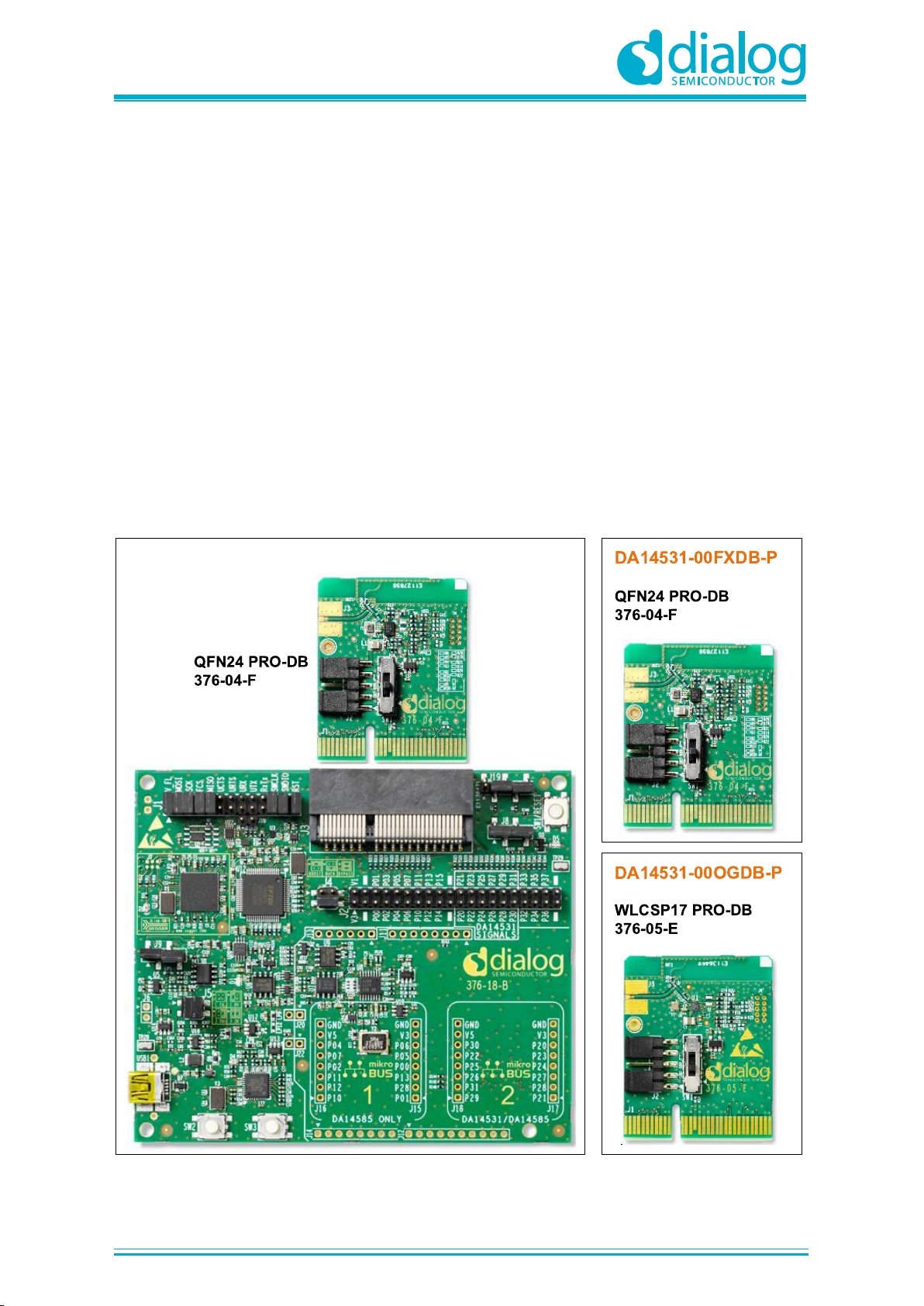
In this document we focus on the DA14531 DK PRO which consists of the following two parts:
● PRO-Motherboard
○ PRO-MB: PCBA reference number 376-18-B
● PRO-daughterboard (PRO-DB) (two options, interchangeable)
○ FCGQFN24 PRO-DB: it uses DA14531-FCGQFN24. PCBA reference number 376-04-F,
○ WLCSP17 PRO-DB: it uses DA14531-WLCSP17. PCBA reference number 376-05-E.
Figure 1 and Table 1 present the part numbers (also ordering code) for the DK PRO
DA14531-00FXDEVKT-P
PRO-MB
376-18-B
DK PRO
Figure 1:DK PRO, DA14531-00FXDEVKT-P DK with PRO-MB and the PRO-DBs

UM-B-114
DA14531 Development Kit Pro Hardware User Manual
User Manual
Revision 1.1
25-Oct-2019
CFR0012
9 of 80
© 2019 Dialog Semiconductor
Table 1: DK PRO part numbers and description
Part number
Description
DA14531-00OGDB-P
WLCSP17 PRO-DB.
Bluetooth Low Energy DA14531 WLCSP17 PRO-daughterboard
DA14531-00FXDB-P
FCGQFN24 PRO-DB
Bluetooth Low Energy DA14531 FCGQFN24 PRO-daughterboard
DA14531-00FXDEVKT-P
DK-PRO
Bluetooth Low Energy Development Kit Pro for DA14531, including PRO-MB
and PRO-DB.
NOTE
When DA14531-00FXDEVKT-P is ordered, the user gets a set of PRO-MB and a FCGQFN24 PRO-DB.
Daughterboard WLCSP17 PRO-DB must be ordered separately.
A single PRO-MB cannot be ordered.
The following sections guide users to understand the system setup, the different available
configuration options, as well as the tools provided to debug, develop, and evaluate the system
performance.
UM-B-114
DA14531 Development Kit Pro Hardware User Manual
User Manual
Revision 1.1
25-Oct-2019
CFR0012
10 of 80
© 2019 Dialog Semiconductor
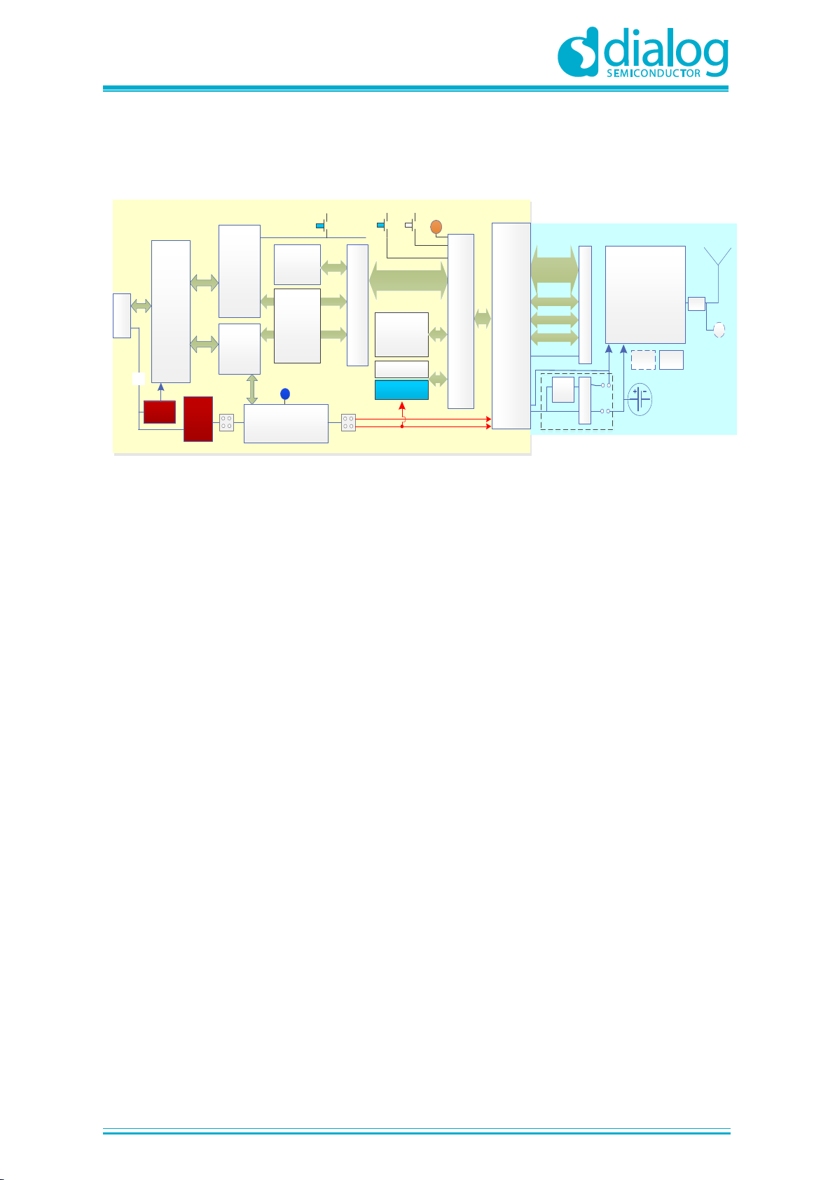
3.1 System Overview
PRO-MB
PRO-DB
UART
bridge
DA14531
BUCK
BOOST
Bypass
Flash
memory
(2Mbit)
32M
3V3
UART
JTAG
RST
VLDO
1.1/1.8/
3.0/3.3V
SMA
JTAG
(SWD)
interface
USB
HUB
Current Sense
circuitry
5V
PRO-MB
LDO
1.1V
R-Multiplexer
Pwr Sw
32K
DA14531
PRO-DB
Level
Translate
J5
J4
SW2 SW3
Mikrobus 1
Mikrobus 2
Arduino
socket
SPI
SW1
D5
UART
JTAG
P2_x
P3_0,1
SPI
MINI B
USB
USB1
V3
V1
SW1
LPF
Config. Header (
J1)
Breakout Header (
J2)
PCI-e connector (J3)
Figure 2: Block Diagram of the DA14531 DK PRO Hardware Platform
3.1.1 Features of DA14531 PRO-DB
● Embedded printed antenna
● RF port output (connector not included)
● DA14531 power mode configuration switch (only for backwards compatibility with DA1458x DK
PRO motherboard)
● Current measurement port to connect external measurement equipment
● Onboard JTAG connector
● Support for coin cell battery (battery holder not included)
3.1.2 Features of DA14531 PRO-MB
● A slot to connect a DA14531 PRO-DB which hosts either the DA14531-FCGQFN24 or the
DA14531-WLCSP17 SoC
● All the power wiring configurations to allow DA14531 PRO-MB to operate in either Buck, Boost,
or Bypass mode
● Dedicated hardware for current measurement that enables Dialog’s SmartSnippets Toolbox
power profiler software as well as any externally connected power measurement device to profile
the power consumption of the system
● Single USB port to provide power and data interfacing to a PC (USB1)
● Onboard JTAG debugger
● Virtual 4-wire UART port
● The DA14531 RESET line is controlled over JTAG by using an onboard push button
● Onboard 2-Mbit SPI data Flash (MX25R2035)
● Multiple voltage options (1.1 V, 1.8 V, 3.0 V, and 3.3V) to supply the DA14531 SoC on the
DA14531 PRO-DB
● Support for coin cell battery (battery holder not included)
● User LEDs and push buttons (to be used with a DA14531 FCGQFN24 PRO-DB)
● Voltage translation for the JTAG and UART signals that allows the current leakage during system
operation to be eliminated
UM-B-114
DA14531 Development Kit Pro Hardware User Manual
User Manual
Revision 1.1
25-Oct-2019
CFR0012
11 of 80
© 2019 Dialog Semiconductor
4 Getting to Know DA14531 DK PRO
4.1 DA14531 PRO-DB
The system on DA14531 PRO-DB consists of the DA14531 SoC, crystals, power section, and radio
section. The system block diagram and the actual components location are presented in Figure 3,
Figure 4, and Figure 5.
U1
DA14531
BUCK
BOOST
Bypass
32M
J3
SMA
U2
LDO
1.1V
R-Multiplexer
Pwr Sw
32K
rst
SW1
Y2
Y1
V3
J2
ANT1
V1
LPF
UART
JTAG
P2_x, P3_0,1
spi
VBAT_Hi
VBAT_Lo
J1-mating connector on PCB
R33
2.2uH
10u
2.2u
For DA145xxDEVKT-P
PRO-MB, set SW1 on
BUCK position
Not Mounted
Figure 3: System Block Diagram of DA14531 PRO-DB
ANT1
PCB ANTENNA
R-Multiplexer
J4
Debug
U1
QFN24
Y2
Y1
32MHz
L1, 2.2μF
CLC
Matching
J3
SMA
J2 – Power
Measurements
SW1
U2
LDO
1.1V
J1 – Mating Connector
Figure 4: DA14531-00FXDB-P, FCGQFN24 PRO-DB_[376-04-F]

UM-B-114
DA14531 Development Kit Pro Hardware User Manual
User Manual
Revision 1.1
25-Oct-2019
CFR0012
12 of 80
© 2019 Dialog Semiconductor
ANT1
PCB ANTENNA
R-Multiplexer
J4
Debug
U1
Y2
Y1
32MHz
L1,
2.2μF
CLC
Matching
J3
SMA
J2 – Power
Measurements
SW1
U2
LDO
1.1V
J1 – Mating Connector
Figure 5: DA14531-00OGDB-P, WLCSP17 PRO-DB_[376-05-E]
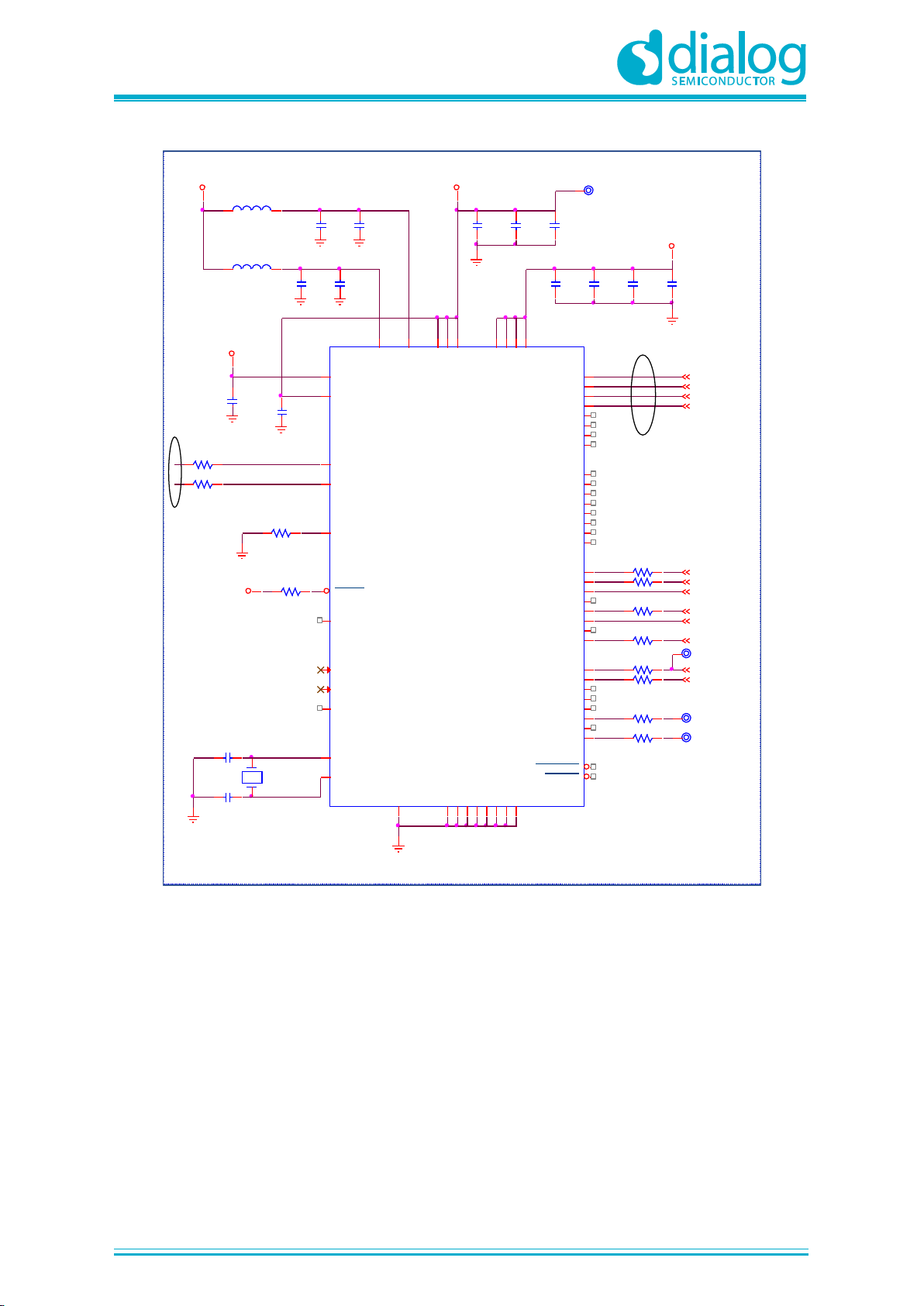
● BLE SoC (U1): DA14531 is an ultra-low power SoC integrating a 2.4 GHz transceiver and an
ARM CortexM0+TM microcontroller with 48 kB of RAM and 32 kB of One-Time Programmable
memory (OTP).
● 32 MHz XTAL (Y1): The main clock of the system is generated from a 32 MHz XTAL which is
connected to the internal clock oscillator. The selected crystal for this reference is the
XRCGB32M000F1H00R0 of Murata.
● 32.768 kHz XTAL (Y2, not assembled by default): A crystal of 32.768 kHz can be placed on
the pins P0_3 and P0_4 of DA14531. A crystal that can be used is the SC20S-7PF20PPM of
SEIKO Instruments.
In most applications the DA14531 can run with good accuracy with its internal RC oscillator
(RCX) and therefore the XTAL32k is not needed. For applications with more demanding
accuracy/drift characteristics, such as timekeeping, using the XTAL32k is considered as a
suitable solution.
By default, Y2 is not assembled on PRO-DB. Internal RC clock is used. P0_3 and P0_4 are
assigned to other SPI data flash (mounted on PRO-MB).
For assembling and utilizing Y2, refer to Appendix F.
● RF section: see section 4.1.2.
● R-Multiplexer: A group of 16 resistors of 0 Ω can be placed/removed as needed in order to
hardwire various peripherals to the DA14531 pins as desired (Appendix D).
To complete a configuration, it is necessary to set/remove jumpers on the DA14531 PRO-MB
accordingly. The default settings are presented in section 5.

UM-B-114
DA14531 Development Kit Pro Hardware User Manual
User Manual
Revision 1.1
25-Oct-2019
CFR0012
13 of 80
© 2019 Dialog Semiconductor
4.1.1 Power Section
The power circuit of DA14531 PRO-DB is designed to support two generations of PRO-MBs:
● PRO-MB: there is no need for the additional circuit. The DCDC power configuration and the
voltage applied to DA14531 SoC are arranged on the PRO-MB (see section 6). In this case, SW1
must be always set to BUCK position.
● In this document the operation with DA14531-00FXDEVKT-P is presented.
U1
DA14531
BUCK
BOOST
Bypass
U2
LDO
1.1V
Pwr Sw
SW1
J2
VBAT_Hi
VBAT_Lo
R33
2.2uH
2.2u
10u
SW1 set to
BUCK Mode
Not
Mounted
V3
V1
NP
PRO-DB
376-04-x
376-05-x
J1-mating connector on PCB
C1
C2
L1
VBAT
Vin
VH-
VL-
Figure 6: DA14531 PRO-DB Power Section
Components:
● U2: it is an LDO which generates V
LDO
= 1.1 V. U2 is supplied from Vin voltage rail and it is
enabled only when SW1 is set for Boost mode. Please notice that the quiescent current of U2 is
measured from the power measurement of PRO-MB. It is disabled for the use with PRO-MB.
● J2: it is used for connecting external power measurement equipment. For current measurements
of sub-μΑ range, users can insert an external equipment. When no external equipment is applied,
jumpers must be applied between 1 and 2 as well as between 4 and 5.
● L1: inductor for the DA14531 DCDC converter in Buck or Boost mode of operation.
● C1: input capacitor for buck mode and output capacitor for boost mode. As input capacitor this
must be equal to 2.2 µF. As an output capacitor, the effective capacitance must be at least 1 μF.
● C2: for the PRO-daughterboard, this capacitor is set to 10 μF.
● SW1: it is a power switch of three positions. Settings:
○ Setting SW1 to position H (Buck) connects the V
BAT_High
and V
BAT_Low
pins of DA14531 to the
voltage rails V1 and V3 of the PRO-MB
○ Setting SW1 to position B (Bypass) connects both V
BAT_High
and V
BAT_Low
pins of DA14531 to
the voltage rail V3 of the PRO-MB
○ Setting SW1 to position L (Boost) connects the V
BAT_Low
pin of DA14531 to the voltage rail
generated from U2 on the PRO-DB
○ For DA14531-00FXDEVKT-P, SW1 must be set to H position (Buck)

UM-B-114
DA14531 Development Kit Pro Hardware User Manual
User Manual
Revision 1.1
25-Oct-2019
CFR0012
14 of 80
© 2019 Dialog Semiconductor
U1
L1
U2
C2
C1
VBAT
VL
VH
GND
Figure 7: Power Section of DA14531 PRO-DB
UM-B-114
DA14531 Development Kit Pro Hardware User Manual
User Manual
Revision 1.1
25-Oct-2019
CFR0012
15 of 80
© 2019 Dialog Semiconductor
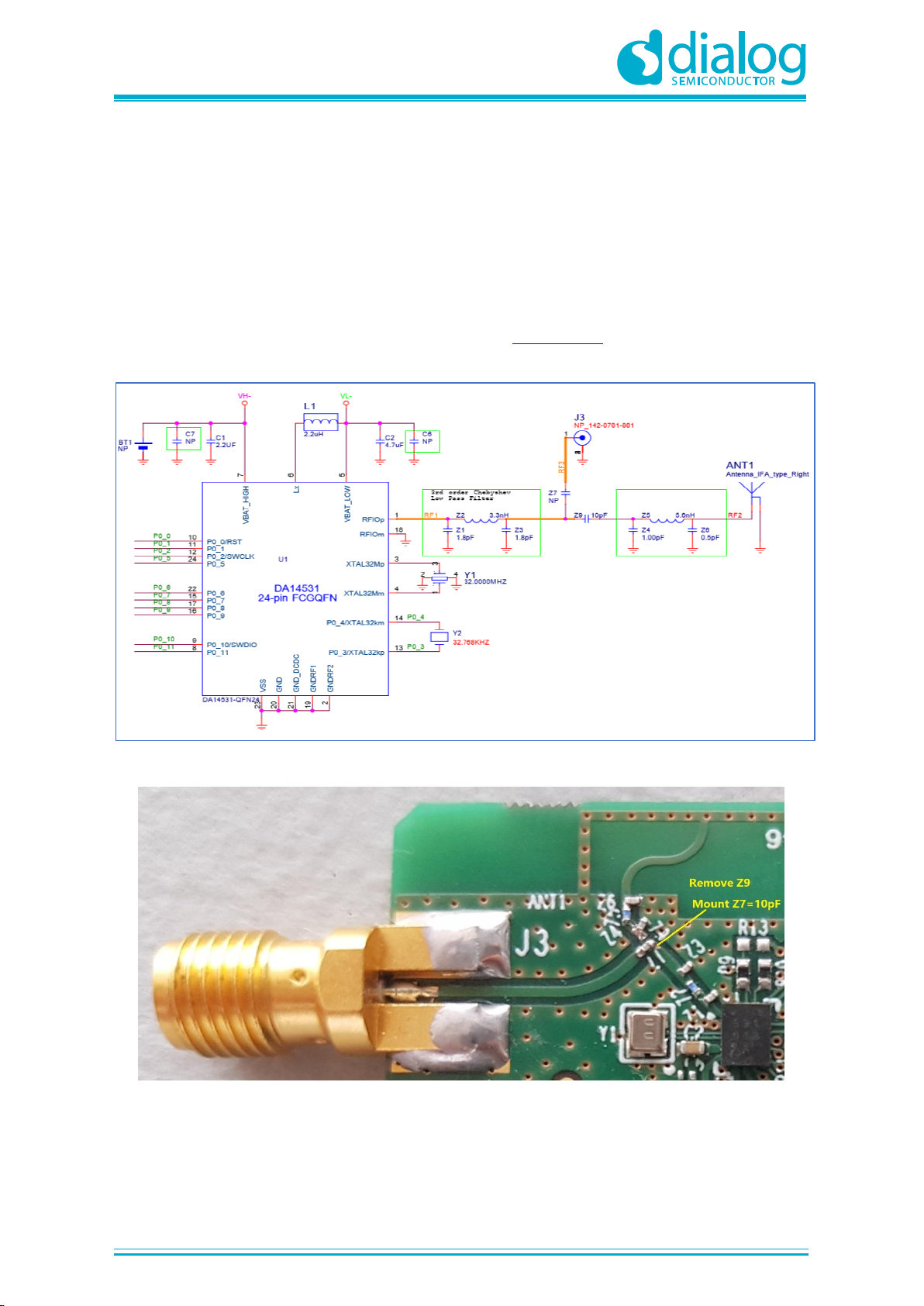
4.1.2 RF Section
A printed F-antenna (ANT1) is used as the radiating element for the DA14531 PRO-DB.
The DA14531 RFIO pin is connected to the printed antenna through a RF stripline and a matching
circuit.
To conduct RF measurements, please proceed with the following hardware modifications (Figure 9):
● Remove Z9
● Assemble Z7 = 10 pF
● Assemble J3, SMA Female Socket 50 Ω Board Edge (142-0761-861 of Cinch Connectivity
Solutions Johnson)
Figure 8: RF Section of DA14531 PRO-DB
Figure 9: Modifications Required for Performing RF Measurements

UM-B-114
DA14531 Development Kit Pro Hardware User Manual
User Manual
Revision 1.1
25-Oct-2019
CFR0012
16 of 80
© 2019 Dialog Semiconductor
4.2 PRO-MB (376-18-B)
The block diagram and the actual component locations of the PRO-MB of DA14531-00FXDEVKT-P
DK PRO are presented on Figure 10 and Figure 11, respectively.
Figure 10: DA145xx DEVKT-P PRO-MB Block Diagram
PRO-DB
Mating header
(J3)
Push Button
Selection header
(J19)
Configuration Header
(J1)
Current
Sense
(J9)
JTAG MCU
(U4)
UART
MCU
(U12)
Voltage
Translator
FLASH
(U2)
VLDO (U5)
VLDO
Selection
(J5)
USB
Connector
(USB1)
GND
GND
GND
User LED &
SW Trigger
(J8)
RESET
Push Button
(SW1)
DA145xx GPIO
Monitoring Header
(J2)
Dialog
Semiconductor
PCB Number
MIKROBUS 2
(J17, J18)
MIKROBUS 1
(J15, J16)
ARDUINO
(J11, J12, J13,
J14)
KEYS
(SW2 & SW3)
DA14531 DCDC
config selection
(J4)
USB HUB
(U11)
Current
Sense Circuit
Figure 11: PRO-MB (376-18-x)
U12
FTDI
UART
U2
Flash
MX25R2 035
3V3
24M
UART
JTAG
RST
VLDO
U4
MCU
with
Segger
JTAG
U11
USB
HUB
Current Sense
circuitry
12M
24M
5V
27M
DA145xxDEVKT-P PRO-MB
J1
Level
Translation
J5
J4
SW2 SW3
Mikrobus 1
Mikrobus 2
Arduino
socket
J3
J2
SPI
SW1 D5
MINI B
USB
USB1
V3
V1

UM-B-114
DA14531 Development Kit Pro Hardware User Manual
User Manual
Revision 1.1
25-Oct-2019
CFR0012
17 of 80
© 2019 Dialog Semiconductor
● USB Hub (U11): connects JTAG and UART interfaces to the PC.
● USB to UART (U12): provides communication between DA14531 UART port and PC. It also
transfers the current measurement samples to PC.
● USB to JTAG (U4): provides communication between DA14531 JTAG and PC.
● USB Connector (USB1): mini-USB connector for power supply and data interfacing to the PC.
● Configuration Header (J1): wiring of the available peripherals to the DA14531 pins is done with
the help of jumpers on J1 (for default configurations) or with jumper wires from J1 to J2 when
custom pin assignments of the peripherals to DA14531 pins are desired.
● DCDC Configuration (J4): selects either Boost, Buck, or Bypass mode for DA14531.
● PRO-DB Mating Header (J3): a connector that accepts the DA145xx PRO-DB board.
● Push Button Selection Header (J19): configures the assignment of onboard push buttons to
certain DA14531 pins.
● Reset Push Button (SW1): push button used to reset DA14531.
● User LED and C-Trig (J8): enables use of the onboard LED (D5) and the software cursor, see
section 5.3.6
● GPIO Monitoring Header (J2): exposes all the pins of the PRO-DB to allow wiring for custom
configurations as well as monitoring of the hardware signals.
● ARDUINO: socket for plugging in an Arduino board. It consists of J11, J12, J13, and J14. It is
multiplexed with mikroBUS (to be used with DA14531-FCGQFN24).
● MikroBUS1 (J15 and J16): the first socket for plugging a mikroBUS click.
● MikroBUS2 (J17 and J18): the second socket for plugging a mikroBUS click.
● Push Buttons (SW2 and SW3): general use push buttons.
● VLDO Selection (J5): selects the output voltage generated for the PRO-DB board (1.1 V, 1.8 V,
3.0 V, or 3.3 V)
● Current Sense Circuit: monitors the current of PRO-DB. It is described in section 8.1.
● Current Sense (J9): enables the current sense circuit (jumpers mounted by default). Also, it
allows the simultaneous connection of an external current measurement instrument in order to
measure and profile the current consumption of D14531.
● RxTx Single Wire UART (J10): Generates RxTx single wire UART by shorting UTX and URX
through a 1 KΩ resistor. Jumpers must be applied to from J10.1 to J1.15 and to from J10.2 to
J15.17.
● J6: manual enable of USB hub voltage regulator. Not in use by default.
● J20: monitoring current sense circuit. Not mounted. No functional use.
● J22: it can provide 6.0 V to PRO-DB. Not mounted. No functional use.

UM-B-114
DA14531 Development Kit Pro Hardware User Manual
User Manual
Revision 1.1
25-Oct-2019
CFR0012
18 of 80
© 2019 Dialog Semiconductor
4.2.1 USB HUB (U11)
The USB HUB of DA14531 PRO-MB is implemented by U11, USB2512B. This chip is supplied with
3.3 V from U13.
The signal PWR_ENABLE is generated from U11 and it is an active high signal. It enables the power
components (LDOs and DCDC converter) for UART, JTAG, and the current sensing circuit. The
system will power up only after the USB HUB has enumerated properly.
Its operation is indicated via the green LED D4 on DA14531 PRO-MB. A 24 MHz crystal (Y3) is
required for the chip operation.
Figure 12: USB HUB Circuitry of DA14531 PRO-MB
4.2.2 USB to UART (U12)
The USB to UART function is implemented by U12, FT2232HL. This chip is supplied with 3.3 V from
U14. A 12 MHz crystal (Y4) is required for the chip operation.
Functions served by U12 are the following:
● Connecting a PC to the UART port of DA14531 SoC
● Connecting a PC to the current sensing circuitry:
○ SPI connection with ADC (U8)
○ Software cursor triggering (C_TRIG)
● Reset capability of the DA14531 SoC through the T_RESET signal (not enabled)
R55 330
TP74
VBUS1
USBDP
R49 100.0K
R50 100.0K
TP20
PWR_EN
R56 100.0K
C59
100nF
C63 18pF
R60 10.0k
C66
100nF
R66 10.0k
USB2512B-AEZG
U11
USBDM_DN1
1
USBDP_DN1
2
USBDM_DN2/PRT_DIS_M2
3
USBDP_DN2/PRT_DIS_P2
4
VDD33_1
5
NC16NC27NC38NC4
9
VDD33_2
10
TEST
11
PRTPWR1/BC_EN1
12
OCS_N1
13
CRFILT
14
VDD33_3
15
PRTPWR2/BC_EN2
16
OCS_N2
17
NC518NC619NC720NC8
21
SDA/NON_REM1/SMBDATA
22
VDD33_4
23
SMBCLK/CFG_SEL0/ SCL
24
HS_IND/CFG_SEL1
25
RESET_N
26
VBUS_DET
27
SUSP_IND /LOCAL_PWR/NON_REM0
28
VDD33_5
29
USBDM_UP
30
USBDP_UP
31
XTALOUT
32
XTALIN/CLKIN
33
PLLFILT
34
RBIAS
35
VDD33_6
36
GND
GND
Y3
24.0000MHZ
C62
100nF
R46
10.0k
D4
Led_Green
2 1
R59 NP
R64 NP
R48
100.0K
L1
CMC 400MA
1
4
2
3
R47
100.0K
C56
100nF
C64 18pF
R58 10.0k
C65
1.0uF
R51
100.0K
R62 NP
VDD_3V3_HU B
VBUS_HUB
VDD_3V3_HU B
VBUS_HUB
R124 NP
USBDM
USBDM_2
USBDP_2
USB HUB
R129 1.00K
C58
100nF
1
2
3
4
5
USB1
USBDP_1
USBDM_1
D7
PRTR5V0U2X,215
GND
1
IO1
2
IO2
3
VCC
4
TP36
USBLED
C73
100nF
C69
100nF
C72
100nF
C68
100nF
C70
100nF
C71
100nF
VDD_3V3_HU B
R54 12.0k
PWR_ENABLE
C57
4.7uF
UM-B-114
DA14531 Development Kit Pro Hardware User Manual
User Manual
Revision 1.1
25-Oct-2019
CFR0012
19 of 80
© 2019 Dialog Semiconductor
Figure 13: USB to UART (U12)
4.2.3 USB to JTAG (U4)
The USB to JTAG function is implemented by U4, SAM3U2CA. On the ROM of U4, software from
SEGGER is loaded. Its operation is indicated via the green LED D2 on the DA14531 PRO-MB. This
chip is supplied with 3.3 V from U14. U14 is enabled by the PWR_ENABLE signal.
Functions served by U4 include:
● Connecting a PC to the JTAG port of DA14531 SoC
● Reset capability of the DA14531 SoC through the T_RESET signal
OSC_EN
TP58
OSC_EN
R152 51 TP64
BCBUS5
TP59
BCBUS7
R114 51
R61 51
AD_SCLK
R63 51
AD_DI
AD_MODE
AD_DO
R68 51
AD_SYNC
R67 51
Y4
12.0000MHZ
R81 NP
C74
18pF
C67
18pF
C55
100nF
C54
10uF
T_RESET
C46
100nF
C45
10uF
3.3V
3.3V
LP6
500mA_470 OHM
C48
100nF
C47
100nF
C49
100nF
VREG
C50
100nF
C51
100nF
C52
100nF
C53
100nF
R65
1.00K
AD_DRDY
3.3V
R82 51
3.3V
C61
4.7uF
C60
100nF
R52 33
R53 33
TP18
VREG
R57
12.0k
LP7
500mA_470 OHM
U12
FT2232HL
VPHY
4
OSCO
3
OSCI
2
AGND
10
DM
7
DP
8
TEST
13
VPLL
9
VCORE12VCORE37VCORE
64
VCCIO20VCCIO31VCCIO56VCCIO
42
GND1GND5GND11GND15GND25GND35GND47GND
51
ADBUS0
16
ADBUS1
17
ADBUS2
18
ADBUS3
19
ADBUS4
21
ADBUS5
22
ADBUS6
23
ADBUS7
24
ACBUS0
26
ACBUS1
27
ACBUS2
28
ACBUS3
29
ACBUS4
30
ACBUS5
32
ACBUS6
33
ACBUS7
34
BDBUS0
38
BDBUS1
39
BDBUS2
40
BDBUS3
41
BDBUS4
43
BDBUS5
44
BDBUS6
45
BDBUS7
46
BCBUS0
48
BCBUS1
52
BCBUS2
53
BCBUS3
54
BCBUS4
55
BCBUS5
57
BCBUS6
58
BCBUS7
59
VREGIN
50
VREGOUT
49
RESET
14
PWREN
60
SUSPEND
36
EECS
63
EECLK
62
EEDATA
61
REF
6
U_CTS
U_RTS
U_TX
U_RX
To
voltage
translator
(UART)
To U11
USB HUB To current
sense
USB SERIAL/SPI INTERFACE

UM-B-114
DA14531 Development Kit Pro Hardware User Manual
User Manual
Revision 1.1
25-Oct-2019
CFR0012
20 of 80
© 2019 Dialog Semiconductor
Figure 14: USB to JTAG (U4)
4.2.4 Voltage Translator
● Voltage translation is applied to the UART and JTAG signals. The voltage translation is from 3.3
V to V
DDIO
and vice versa.
● V
DDIO
is generated from U1A, where V3 (V
BAT_HIGH
) is used as a reference. Consequently, there is
no additional power consumption on the power circuitry of DA14531 PRO-MB due to voltage
translation.
Figure 15: Voltage Translator Circuitry of DA14531 PRO-MB
R8 150
R12
10.0k
TP1
VDD_CR
C6
100nF
R11
10.0k
LP2
500mA_470 OHM
VBUS_HUB
R14 150
R10
10.0k
C18 18pF
C7
100nFC8100nF
TP3
C16 10nF
C17 18pF
TP9
DBLED
C9
100nF
R13
100.0K
C10
100nF
TP8
C11
100nF
R19 39
C14
10uF
R21
6.8k
C19
10pF
C12
100nF
R20 39
C15
10uF
TP6
C13
100nF
J7
TagConnect
1 2
3 4
5 6
TP7
TP10
TP5
TFBGA-100
ATSAM3U2CA-CU
U4
XIN
A2
XOUT
A3
XIN32
A10
NRST
B7
XOUT32
B10
TMS/SWDIO
C7
NRSTB
C8
JTAGSEL
C9
TST
D7
FWUP
D8
TCK/SWCLK
A7
TDO/TRACESWO
B8
TDI
B9
ERASE
D6
VBG
A1
DFSDP
C1
DHSDP
C2
VDDBU
C10
DFSDM
D1
DHSDM
D2
VDDPLL
D3
VDDCORE1
D4
VDDIO3
E6
VDDCORE2
E7
VDDIO1F3VDDIO2
F5
VDDCORE4F9VDDCORE5G5VDDCORE6
H1
ADVREF
J3
VDDANA
K2
AD12BVREF
K4
PB17
A4
PB21
A5
PB23
A6
VDDIN
A8
VDDOUT
A9
VDDCORE3
B1
GNDUTM I
B2
VDDUTM I
B3
PB10
B4
PB18
B5
PB24
B6
GNDPLL
C3
PB14
C4
PB19
C5
PB22
C6
PB20
D5
PA11/PGMD3/URXD
D9
PA12/PGMD4/UTXD
D10
PA29
E1
GND2
E2
PA28
E3
PB9
E4
GNDBU
E5
PA10/PGMD2
E8
PA9/PGMD1
E9
PA8/PGMD0
E10
PB1
F1
PB12
F2
PA31
F4
GND1
F6
PB16
F7
PA6/PGMM2
F8
PA7/PGMM3
F10
PB11
G1
PB2
G2
PB0
G3
PB13
G4
GND3
G6
PB15
G7
PA3/PGMNVALID
G8
PA5/PGMM1
G9
PA4/PGMM0
G10
PB5
H2
PA27
H3
PA22/PGMD14
H4
PA13/PGMD5
H5
PA15/PGMD7
H6
PA18/PGMD10
H7
PA24
H8
PA1/PGMRDY
H9
PA2/PGMNOE
H10
PB6
J1
PB8
J2
PA30
J4
PB3
J5
PA16/PGMD8
J6
PA19/PGMD11
J7
PA21/PGMD13
J8
PA26
J9
PA0/PGMNCMD
J10
PB7
K1
GNDANA
K3
PB4
K5
PA14/PGMD6
K6
PA17/PGMD9
K7
PA20/PGMD12
K8
PA23/PGMD15
K9
PA25
K10
VDD_3V3_PERF
VDD_CORE VDD_3V3_PERF
VDD_3V3_PERFVDD_CORE
VDD_CORE
VDD_3V3_PERF
VDD_3V3_PERF
TP4
XOUT
USB_DP
PA15
PA18
VDD_3V3_PERF
DFSDM
PA22
DFSDP
VBG
TDIin
PA29
PA4
To VDDBU
NRSTB
FWUP
TCK/SWCLK
TRSTout
TRSTin
PA17
TDIout
TRSTout
TRSTin
Needed for Segger software
NRST
TDIout
TDIin
NRST
TDI
For programming SAM3U2C
ERASE
XIN
SWO/TDO
A_D4_2
NRST
TP76
SWDIO
TP77
SWCLK
D2
Led_Green
21
R18
330
TMS/SWDIO
T_SWCLK
T_SWDIO
T_RESET
R9
150
USBDP_1
USBDM_1
Y1
12.0000MHZ
R16 150 R17 100
R15 100

UM-B-114
DA14531 Development Kit Pro Hardware User Manual
User Manual
Revision 1.1
25-Oct-2019
CFR0012
21 of 80
© 2019 Dialog Semiconductor
4.2.5 Power Section
● The DA14531 SoC in the DA14531 PRO-MB is supplied from the V
LDO
voltage rail generated
from U5, LDO.
● V
LDO
can be set to four different voltage levels. This is arranged by J5 settings.
● Generated power flows through the current sensing circuit to the DA14531 PRO-DB power
supply pins:
○ V1 is connected to V
BAT_LOW
○ V3 is connected to V
BAT_HIGH
● By applying proper jumpers on header J4, users can enable buck, boost, or bypass mode of
operation for the DA14531 DCDC converter.
● For power configuration settings, refer to section 6.
VLDO
U5
U1
DA14531
BUCK
BOOST
Bypass
U2
LDO
1.1V
Pwr Sw
SW1
J2
VBAT_Hi
VBAT_Lo
R33
2.2uH
2.2u
10u
Set SW1
for BUCK
Not
Mounted
V3
V1
NP
PRO-MB
376-18-B
PRO-DB
376-04-F
376-05-E
J1-mating connector on PCB
C1
C2
L1
VBAT
Vin
Current
Sense
circuitry
J5
J4
VLDO
J9
Figure 16: Power Topology for DA14531 PRO-MB and PRO-DB
Figure 17: Power Circuit for DA14531 PRO-MB

UM-B-114
DA14531 Development Kit Pro Hardware User Manual
User Manual
Revision 1.1
25-Oct-2019
CFR0012
22 of 80
© 2019 Dialog Semiconductor
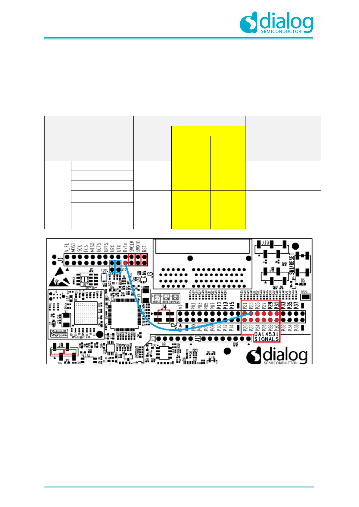
5 GPIOs and Pin Assignment and Functions of DA14531 DK PRO
All signals of the DA14531 PRO-DBs are provided to DA14531 PRO-MB. The signal names are
specific for the PRO-MB and do not have the same names as the signals of the PRO-DBs. The
reason is that the PRO-MB can be used for both DA14531 SoC and DA1458x family of SoCs,
whereas DA14531 SoC has fewer pins than DA1458x SoCs.
Please note that signals of DA14531 SoC (P0_0 to P0_10) are provided to ports 2 and 3 of the PROMB (P2_0 to P2_9, P3_0, and P3_1). So, on the breakout header J2 of the PRO-MB, the pins of
DA14531:
● P0_0 to P0_11 are mapped to P2_x, P3_0 and P3_1 for FCGQFN24
● P0_0 to P0_5 are mapped to P2_0 to P2_5 for WLCSP17
Figure 18: J2, Breakout Header of DA14531 PRO-MB
Due to the low GPIO count, function multiplexing is applied. Every function of the DA14531 DK PRO
is practically dependent on the PRO-MB GPIO configuration, as the configuration of the PRO-DB
requires soldering and de-soldering of resistors.
The PRO-MB configuration is realized with jumpers or cables. J1 on the PRO-MB is the main
configuration header (Figure 19).
PRO-DB configuration is also feasible. Please refer to Appendix D.

UM-B-114
DA14531 Development Kit Pro Hardware User Manual
User Manual
Revision 1.1
25-Oct-2019
CFR0012
23 of 80
© 2019 Dialog Semiconductor
Figure 19: J1, Configuration Header on DA14531 PRO-MB
The DA14531 PRO-DB GPIO pin assignment as well the configuration settings for the GPIOs of the
PRO-MB are presented below. The DA14531 DK PRO signals connectivity is depicted in the Table 2
where the GPIOs of DA14531 PRO-DB are mapped to the breakout header (J2) and the
configuration header (J1) of PRO-MB.
Table 2 also presents the available functions for every GPIO of DA14531.
Table 2: PRO-MB to DA14531 Signal Correspondence and Function Multiplexing
PRO_MB
Signals
DA14531 PRO-DB
Function 1
Function 2
Function 3
Signals
J2
FCGQFN24
WLCSP17
Enabled by J1
Settings
mikroBUS & Arduino
(MBUS & ARD)
Enabled by
Jumpers
P0_0
P0_4
P0_4
SCK
J1:5-6
(Default)
SCK_1
MBus1/ARD
P0_1
No available pins from
DA14531
AN_1
MBus1/ARD
P0_2
TX_1
MBus1/ARD
P0_3
P0_1
P0_1
FCS
J1:7-8
(Default)
A2
ARD
P0_4
P0_0
P0_0
UTX
J1:17 to
J2:21
(cable)
SDA_1
MBus1/ARD
P0_5
P0_3
P0_3
MISO
J1:9-10
(Default)
MISO_1
MBus1
URX
J1:15-16
P0_6
P0_0
P0_0
MOSI
J1:3-4
(Default)
MOSI_1
MBus1
SW2
J19:1-2
UCTS
J1:11-12
P0_7
P0_4
P0_4
URTS
J1:13 to
J2:25
(cable)
SCL_1
MBus1/ARD
SWCLK
P0_2
P0_2
SWCLK
J1:21-22
(Default)
SWDIO
P0_10
P0_5
SWDIO
J1:23-24
(Default)
P1_0
P0_9
PWM_1
MBus1/ARD
LED
J8:1-2
(Default)
P1_1
P0_10
RX_1
MBus1/ARD
SW3
J19:4-5
P1_2
No Available pins from
DA14531
INT_1
MBus1/ARD

UM-B-114
DA14531 Development Kit Pro Hardware User Manual
User Manual
Revision 1.1
25-Oct-2019
CFR0012
24 of 80
© 2019 Dialog Semiconductor
PRO_MB
Signals
DA14531 PRO-DB
Function 1
Function 2
Function 3
Signals
J2
FCGQFN24
WLCSP17
Enabled by J1
Settings
mikroBUS & Arduino
(MBUS & ARD)
Enabled by
Jumpers
P1_3
P0_11
CS_1
MBus1
CTRIG
J8:3-4
(Default)
P2_0
P0_0
P0_0
RST
J1: 25-26
(Default)
MOSI_2
MBus2
P2_1
P0_1
P0_1
AN_2
ARD
P2_2
P0_2
P0_2
SCL_2
MBus2/ARD
P2_3
P0_3
P0_3
MISO_2
MBus2
P2_4
P0_4
P0_4
SCK_2
MBus2
P2_5
P0_5
P0_5
RxTx
J1:19-20
TX_2
MBus2/ARD
J10:1 to
J1:15
J10:2 to
J1:17
P2_6
P0_6
RX_2
MBus2/ARD
P2_7
P0_7
CS_2
MBus2/ARD
P2_8
P0_8
SDA_2
MBus2/ARD
P2_9
P0_9
PWM_2
MBus2
P3_0
Note1
BRSTn
MBus1,2/ARD
P3_1
P0_11
INT_2
ARD
SW2
J19:2-3
(Default)
P3_2
No available pins from
DA14531
D2
ARD
P3_3
D3
ARD
P3_4
D4
ARD
P3_5
D5
ARD
P3_6
D6
ARD
P3_7
D7
ARD
Note 1 P3_10 is assigned to P0_10 (SWDIO) through the resistor R11 on DA14531 FCGQFN24 PRO-DB.
R11 is not populated.
5.1 DA14531 WLCSP17 PRO-DB, Default Setup
● The default configuration of D14531 WLCSP17 PRO-DB is:
○ Reset
○ JTAG and SPI data flash
● Dual UART or full UART are not enabled. To enable UART, refer to section 5.3.4
● Crystal 32.768 kHz is not enabled. To enable the crystal 32.768 kHz, refer to section F.1
● Resistor matrix for DA14531 WLCSP17 PRO-DB (and DA145xx-DEVKT-P PRO-MB signals are
presented in E.1.
● Please note that signals of DA14531 WLCSP17 PRO-DB are renamed on PRO-MB. The reason
is that PRO-MB can be used for the PRO-DBs of DA1458x family

UM-B-114
DA14531 Development Kit Pro Hardware User Manual
User Manual
Revision 1.1
25-Oct-2019
CFR0012
25 of 80
© 2019 Dialog Semiconductor
● For detailed description of the connection capabilities of DA14531 WLCSP17 PRO-DB circuitry,
please refer to Appendix D
Table 3: DA14531 WLCSP Signals Assignment
DA14531 PRO-DB
WLCSP17
PRO-MB
Signals
Signal Name
J1 & J2
Pin Number
Functions Enabled by Jumpers
Function
J1 Pins
P0_0
P2_0
J2:21
RST
J1:26
RST
J1: 25-26 (Default)
P0_6
J2:11
MOSI (Flash)
J1:3-4 (Default)
P0_1
P2_1
J2:22
P0_3
J2:8
FCS (Flash)
J1:7-8 (Default)
P0_2
P2_2
J2:23
SW_CLK
J1:22
SWCLK
J1:21-22 (Default)
P0_3
P2_3
J2:24
P0_5
J2:10
MISO (Flash)
J1:9-10 (Default)
P0_4
P2_4
J2:25
P0_0
J2:5
SCK (Flash)
J1:5-6 (Default)
P0_5
P2_5
J2:26
SW_DIO
J1:24
SWDIO
J1:23-24 (Default)
5.2 DA14531 FCGQFN24 PRO-DB, Default Setup
● The default configuration of DA14531 FCGQFN24 PRO-DB is:
○ Reset
○ JTAG
○ SPI data flash
○ and single wire UART
To enable these functions, apply the appropriate jumpers to the DA14531 PRO-MB
● Dual UART or full UART are not enabled. To enable UART, see section 5.3.4
● Crystal 32.768 kHz is not enabled. For enabling crystal 32.768 kHz, refer to section F.1
● Resistor matrix for FCGQFN24 PRO-DB and DA145xx-DEVKT-P PRO-MB signals are presented
in section E.2.
● Please note that signals of DA14531 FCGQFN24 PRO-DB are renamed on PRO-MB. The
reason is that PRO-MB can be used for the daughterboards of DA1458x family
● For detailed description of the connection capabilities of DA14531 FCGQFN24 PRO-DB circuitry,
please refer to Appendix D
UM-B-114
DA14531 Development Kit Pro Hardware User Manual
User Manual
Revision 1.1
25-Oct-2019
CFR0012
26 of 80
© 2019 Dialog Semiconductor
Table 4: DA14531 FCGQFN24 PRO-DB and PRO-MB Signals Assignment (Default)
DA14531
PRO-DB
FCGQFN24
PRO-MB
Signals
Signal
Name
J1&J2 Pin
Number
Functions Enabled by
Jumpers
Multiplexed Functions
Function
Jumpers
Function
Interface
Header
Pins
Numbers
P0_0
P2_0
J2:21
MOSI_2
MBus2
J17:6
RST
J1:26
J1: 25-26
(Default)
P0_6
J2:11
MOSI
(Flash)
J1:3-4
(Default)
P0_1
P2_1
J2:22
AN_2
Arduino
J12:9
P0_3
J2:8
FCS
(Flash)
J1:7-8
(Default)
P0_2
P2_2
J2:23
SCL_2
MBus2 &
Arduino
J18:5
SW_CLK
J1:22
SWCLK
J1:21-22
(Default)
P0_3
P2_3
J2:24
MISO_2
MBus2
J17:5
P0_5
J2:10
MISO
(Flash)
J1:9-10
(Default)
P0_4
P2_4
J2:25
SCK_2
MBus2
J17:4
P0_0
J2:5
SCK
(Flash)
J1:5-6
(Default)
P0_5
P2_5
J2:26 and
J1:20
RxTx
J1: 19-20
J10:1-J1:15
J10:2-J1:17
TX_2
MBus2 &
Arduino
J18:4 to
J12:4
P0_6
P2_6
J2:27
RX_2
MBus2 &
Arduino
J18:3 to
J12:5
P0_7
P2_7
J2:28
CS_2
MBus2 &
Arduino
J17:3
toJ12:6
P0_8
P2_8
J2:29
SDA_2
MBus2 &
Arduino
J18:6
toJ14:1
P0_9
P2_9
J2:30
PWM_2
MBus2
J18:1
P1_0
J2_13
LED
J8:1-2
(Default)
P0_10
SW_DIO
J1:24
SWDIO
J1:23-24
(Default)
P0_11
P3_1
J2:31
SW2
J19:2-3
(Default)
INT_2
Arduino
J14:2
P1_3
J2:16
C_TRIG
J8:3-4
(Default)
UM-B-114
DA14531 Development Kit Pro Hardware User Manual
User Manual
Revision 1.1
25-Oct-2019
CFR0012
27 of 80
© 2019 Dialog Semiconductor
5.3 PRO-MB Setup
The PRO-MB provides several debug interfaces and tools that can be used for development.
The DA14531 pin assignment for the available functions are presented in the following sections.
5.3.1 Reset
At power-on and before booting in the chip, reset is active high, and it is assigned to on P0_0. After
booting, reset assignment and operation is handled by software.
● On a DA14531 PRO-DB, the reset signal provided by the PRO-MB is connected to P0_0 for
WLCSP17 and FCGQFN24 through a 1 kΩ resistor
● On the PRO-MB, reset can be enabled either from the JTAG interface (T-RESET) or by pressing
the push button SW1
Please note that, to enable reset on an application, P0_0 must be enabled in both hardware and
software
Figure 20: RESET Circuit on DA14531 PRO-MB
Figure 21: Reset Pin Assignment on PRO-DBs for FCGQFN24 and WLCSP17

UM-B-114
DA14531 Development Kit Pro Hardware User Manual
User Manual
Revision 1.1
25-Oct-2019
CFR0012
28 of 80
© 2019 Dialog Semiconductor
5.3.2 JTAG
JTAG uses the Serial Wire Debug (SWD) protocol and consists of the SWDIO and SWCLK lines.
Depending on the package of DA14531, the SWDIO signal is assigned to different pins (Table 5).
Table 5: Configuration Settings for JTAG In DA14531 DK Pro
Function
The Signals
Comments
PRO-MB
DA14531 PRO-DB
Enabled by Jumpers
J2
FCGQFN24
WLCSP17
SW_CLK
J1:21-22 (Default)
SWCLK
P0_2
P0_2
SW_DIO
J1:23-24 (Default)
SWDIO
P0_10
P0_5
JTAG signals are also available on DA14531 PRO-DBs on headerJ4 (Figure 22).
Figure 22: Optional Debug Port
5.3.3 SPI Data Flash (U2)
SPI data flash is enabled by default. The SPI data flash is the MX25R2035 from Macronix (2 Mbit)
and located on DA14531 PRO-MB.
Ext-SPI slave mode is used to connect DA14531 to SPI data flash.
The flash is absolutely isolated from the rest of the circuit unless appropriate jumpers are. The
configuration for SPI data flash is presented in Table 6.
Table 6: Configuration Settings for SPI Data Flash in DA14531 DK Pro
Function
The Signals
Comments
PRO-MB
DA14531 PRO-DB
Enabled by Jumpers
J2
FCGQFN24
WLCSP17
MOSI
J1:3-4 (Default)
P0_6
P0_0
P0_0
FCS
J1:7-8 (Default)
P0_3
P0_1
P0_1
MISO
J1:9-10 (Default)
P0_5
P0_3
P0_3
SCK
J1:5-6 (Default)
P0_0
P0_4
P0_4

UM-B-114
DA14531 Development Kit Pro Hardware User Manual
User Manual
Revision 1.1
25-Oct-2019
CFR0012
29 of 80
© 2019 Dialog Semiconductor
V_FL
J1:1-2 (Default)
V3
VH-
VH-
Flash Voltage.
It is supplied with the voltage rail
of V
BAT_HIGH
Figure 23: SPI Data Flash Circuit in DA14531 DK Pro
5.3.4 UART
In the DA14531 DK PRO, UART is not enabled by default. Three modes can be used: single-wire
UART (section 0), 2-wire UART (section 5.3.4.1), or full UART (section 5.3.4.2). For the 2-wire or full
UART, the SPI data flash must be disabled.
Any GPIO pin can be set as UART. In the DA14531 DK PRO, specific pins are used for UART
signals (Table 7). Use short cables on DA14531 PRO-MB to bridge J2 pins (P2_0 to P3_1) and pins
of J1 (odd pin-numbers).
Table 7: UART Signals Assignment in DA14531 DK PRO
Function
The signals
Comments
PRO-MB
DA14531 PRO-DB
J2
FCGQFN24
WLCSP17
UTX
2-wire or Full Transmit
P2_0
P0_0
P0_0
Signals reused for SPI
Data Flash
URX
2-wire or Full UART
Receive
P2_1
P0_1
P0_1
UCTS
2-wire or Full UART
Clear to Send
P2_3
P0_3
P0_3
URTS
2-wire or Full UART
Request To Send
P2_4
P0_4
P0_4
RxTx
Single wire UART
Receive and Transmit
P2_3 P0_3
P2_5
P0_5
UM-B-114
DA14531 Development Kit Pro Hardware User Manual
User Manual
Revision 1.1
25-Oct-2019
CFR0012
30 of 80
© 2019 Dialog Semiconductor
Single-wire UART
● DA14531-WLCSP17: use P0_3 for single-wire UART. It is supported from SmartSnippet Toolbox.
A wire bridge must be used on PRO-MB.
● DA14531-FCGQFN24: use P0_5 for single-wire UART. it is supported from SmartSnippet
Toolbox. There is no need for bridge wire (Table 8).
Table 8: Single-wire UART Pin Assignment
Function
The Signals
Comments
PRO-MB
DA14531 PRO-DB
Enabled by Jumper/Wire-Bridge
J2
FCGQFN24
WLCSP17
RxTx
Jumper: J1: 19-20
P2_5
P0_5
No need to disable SPI Data
Flash.
Jumper: J10:1-J1:15
Jumper: J10:2-J1:17
wire: J1:19 to J2:24
P2_3
P0_3
In order not to conflict with
MISO, disable SPI Data
Flash. Remove jumpers:
J1: 1-2/J1: 3-4/J1:5-6/J1:78/J1:9-10
Jumper: J10:1-J1:15
Jumper: J10:2-J1:17
Figure 24: Single-wire UART for DA14531 WLCSP17 PRO-DB
5.3.4.1 2-wire UART Configuration
● UTX and URX signals are multiplexed with FCS (chip select) and MISO of SPI data bus
● Two wires are required to connect UTX and URX to DA14531 PRO-DBs
● Disable SPI data flash by removing jumpers on J1
● JTAG and Reset can be used

UM-B-114
DA14531 Development Kit Pro Hardware User Manual
User Manual
Revision 1.1
25-Oct-2019
CFR0012
31 of 80
© 2019 Dialog Semiconductor
Table 9: 2-wire UART Pin Assignment
Function
The Signals
Comments
PRO-MB
DA14531 PRO-DB
Enabled by Wire-Bridge
J2
FCGQFN24
WLCSP17
UTX
J1:17 to J2:21
P2_0
P0_0
P0_0
Remove jumper J1: 3-4
URX
J1:15 to J2:22
P2_1
P0_1
P0_1
Remove jumper J1: 7-8
Figure 25: 2-wire UART Connectivity
5.3.4.2 Full UART (4-wire) Configuration
● UTX and URX as well as UCTS and URTS signals are multiplexed with FCS, MISO, MOSI, and
SCK of the SPI data bus, respectively
● Four wires are required to connect UART signals to DA14531 PRO-DBs
● Disable SPI data flash by removing jumpers on J1
● JTAG and Reset can be used
Table 10: Full UART Pin Assignment
Function
The Signals
Comments
PRO-MB
DA14531 PRO-DB
Enabled by Wire-Bridge
J2
FCGQFN24
WLCSP17
UTX
J1:17 to J2:21
P2_0
P0_0
P0_0
Remove jumper J1: 3-4
URX
J1:15 to J2:22
P2_1
P0_1
P0_1
Remove jumper J1: 7-8
UCTS
J1:11 to J2:24
P2_3
P0_3
P0_3
Remove jumper J1: 9-10
URTS
J1:13 to J2:25
P2_4
P0_4
P0_4
Remove jumper J1: 5-6

UM-B-114
DA14531 Development Kit Pro Hardware User Manual
User Manual
Revision 1.1
25-Oct-2019
CFR0012
32 of 80
© 2019 Dialog Semiconductor
Figure 26: Full UART (4-wire) Connectivity
5.3.5 Push Buttons
● There are two available push buttons, SW2 and SW3, on DA14531 PRO-MB
● Push buttons are available mainly for DA14531 FCGQFN24 PRO-DB
● SW3 is connected to SWDIO signal (P0_10 for DA14531 FCGQFN24). Users must enable SW3
on software
● SW2 is assigned to P0_11 of DA14531 FCGQFN24 (P3_1 of PRO-MB)
Figure 27: Miscellaneous Peripherals

UM-B-114
DA14531 Development Kit Pro Hardware User Manual
User Manual
Revision 1.1
25-Oct-2019
CFR0012
33 of 80
© 2019 Dialog Semiconductor
Table 11: Configuration settings for push buttons
Function
PRO-MB
The Signals
Comments
DA14531 PRO-DB
Enabled by Jumpers
J2
FCGQFN24
WLCSP17
SW2
J19:1-2
P0_6
P0_0
P0_0
Reused in Flash, Reset, UART,
and mikroBUS. Before enabling
the signal, ensure that there is no
conflict on system operation.
J19:2-3
(Default)
P3_1
P0_11
SW3
J19:4-5
P1_1
P0_10
P0_10 is not available on
DA14531 for this function.
5.3.6 User LED (D5) and C-Trig (Software Cursor)
The user LED (D5) and the software cursor trigger (C-trig) are available only for DA14531
FCGQFN24 PRO-DB. The user LED is enabled by default and it is driven from P0_9 of DA14531
FCGQFN24 PRO-DB (P1_0 of PRO_MB). The C-Trig is used by the power profiler of SmartSnippet
Toolbox to enable the software cursor. It is connected to P0_11 of DA14531 FCGQFN24 PRO-DB
through a 1 kΩ resistor.
Figure 28: User LED and Software Trigger Circuit and Jumpers
Table 12: Configuration settings for miscellaneous peripherals
Function
The Signals
Comments
PRO-MB
DA14531 PRO-DB
Enabled by Jumpers
J2
FCGQFN24
WLCSP17
LED
J8:1-2 (Default)
P1_0
P0_9
NA
C_TRIG
J8:3-4 (Default)
P1_3
P0_11
NA
Also assigned to SW2.
In order not to disturb C-
TRIG operation, remove
the jumper from J18:2-3.

UM-B-114
DA14531 Development Kit Pro Hardware User Manual
User Manual
Revision 1.1
25-Oct-2019
CFR0012
34 of 80
© 2019 Dialog Semiconductor
5.3.7 mikroBUS 2 Interface
● mikroBUS 2 is used for DA14531 PRO-DB
● Two female headers (8 position 0.100", through hole, socket type) must be mounted on J17 and
J18
● DA14531 FCGQFN24 PRO-DB is suitable for mikroBUS operation due to its available pins
● SPI data bus is shared with SPI data flash or UART
Table 13: mikroBUS 2 Signals
Function
The Signals
Comments
PRO-MB
DA14531 PRO-DB
Available on Headers
J2
FCGQFN24
WLCSP17
MOSI_2
J17:5
P2_0
P0_0
P0_0
Also used from SPI Data Flash or
UART.
SCL_2
J18:5
P2_2
P0_2
P0_2
MISO_2
J17:6
P2_3
P0_3
P0_3
SCK_2
J17:4
P2_4
P0_4
P0_4
TX_2
J18:4
P2_5
P0_5
P0_5
Used for SWDIO of WLCSP17.
Used for single-wire UART of
FCGQFN24.
RX_2
J18:3
P2_6
P0_6
CS_2
J17:3
P2_7
P0_7
SDA_2
J18:6
P2_8
P0_8
PWM_2
J18:1
P2_9
P0_9
BRSTn
J17:2
P3_0
It is not enabled.
BRSTn can be connected to P0_10
(SWDIO) by mounting R11 on
FCGQFN24 PRO-DB.
V3
J17:7 V
BAT_HIGH
The same voltage rail applied to
V
BAT_HIGH
pin of DA14531 SoC.
V5
J18:7
Voltage provided from USB port,
V
BUS_HUB
= 5 V through R305.
Figure 29: MikroBus 2 Circuit

UM-B-114
DA14531 Development Kit Pro Hardware User Manual
User Manual
Revision 1.1
25-Oct-2019
CFR0012
35 of 80
© 2019 Dialog Semiconductor
5.3.8 Arduino Interface
Four female headers (0.100", through hole, socket type) must be mounted on J11, J12, J13, and J14.
Table 14: Arduino Signals
Function
The Signals
Comments
PRO-MB
DA14531 PRO-DB
Available on Headers
J2
FCGQFN24
WLCSP17
SCK_1
J13:4
P0_0
P0_4
P0_4
Multiplexed with SPI, UART, and
other Arduino Interface signals.
A2
J13:3
P0_3
P0_1
P0_1
SDA_1
J12:1
P0_4
P0_0
P0_0
SCL_1
J12:2
P0_7
P0_4
P0_4
PWM_1
J12:3
P1_0
P0_9
Multiplexed with User LED.
Can remove J8:1-2.
RX_1
J13:6
P1_1
P0_10
Multiplexed with SWDIO of
DA14531 FCGQFN24 PRO-DB. It
must be enabled in software.
AN_2
J12:9
P2_1
P0_1
P0_1
Multiplexed with SPI, UART, and
other Arduino Interface signals.
SCL_2
J12:10
P2_2
P0_2
P0_2
TX_2
J12:4
P2_5
P0_5
P0_5
Used for SWDIO of WLCSP17.
Used for single-wire UART of
FCGQFN24.
RX_2
J12:5
P2_6
P0_6
CS_2
J12:6
P2_7
P0_7
SDA_2
J14:1
P2_8
P0_8
BRSTn
J11:3
P3_0
It is not enabled.
INT_2
J14-2
P3_1
P0_11
V3
J11:4 V
BAT_HIGH
The same voltage rail applied to
V
BAT_HIGH
pin of DA14531 SoC.
V5
J11:5
VBUS_HUB voltage provided from
USB port.

UM-B-114
DA14531 Development Kit Pro Hardware User Manual
User Manual
Revision 1.1
25-Oct-2019
CFR0012
36 of 80
© 2019 Dialog Semiconductor
6 How to Configure Power of DA14531 DK PRO
On DA14531 DK PRO, users can:
● Set DA14531 SoC on Buck, Boost, or Bypass mode (applied to J5 on PRO-MB), Table 15
● Provide four different voltage rails to DA14531 SoC, that is, 1.1 V, 1.8 V, 3.0 V, and 3.3 V
(default) (applied on J4 on PRO-MB), Table 15
Jumper settings of J9 enables the current sensing circuit, Table 16. Jumpers are applied by default.
On DA14531 PRO DBs (WLCSP17 and FCGQFN24), users must set SW1 to buck position
permanently. The power circuit consisting of U2 and SW1 on PRO-DBs is not needed.
Figure 30: DA14531 PRO-DB Configuration and DA14531 PRO-MB Jumpers

UM-B-114
DA14531 Development Kit Pro Hardware User Manual
User Manual
Revision 1.1
25-Oct-2019
CFR0012
37 of 80
© 2019 Dialog Semiconductor
Table 15: DA14531 DCDC Configuration and Input Voltage
Board
Configuration
Setting
Comments
PRO-MB
J9:1-2
J9:3-4
Enabling the current sensing
circuit of PRO-MB
1.1 V
J5: no jumper
Voltage levels of V
LDO
V
LDO
generates V1 and V3
1.8 V
J5: 1-3
3.0 V
J5: 2-4
3.3 V (Default)
J5: 1-3
J5: 2-4
Boost
J4:1-2
V
BAT_LOW
supplied by V1,
enabling Boost mode
Buck (Default)
J4:3-4
J4:3-4
V
BAT_HIGH
supplied by V3,
enabling Buck mode
Bypass
J4:1-2
V
BAT_HIGH
and V
BAT_LOW
are
supplied from V3 and V1,
respectively, enabling bypass
mode
DA14531 PRO-DB
J1:1-2
J1:4-5
jumpers applied
Buck Mode
SW1: H
Table 16: Jumper Settings for J9
Jumper on J9
Function
Comments
J9: 1-2
J9: 3-4
V
LDO
supplies PRO-DB
Current sensing circuit enabled
See Figure 16
J9:2-3
V
LDO
supplies PRO-DB
Current sensing circuit is
bypassed
See Figure 16
J9: 3-4
BT1 supplies PRO-DB
Current sensing circuit enabled
BT1 must be mounted
See Figure 16
Example: to provide 3.0 V in buck mode, proceed with the following actions:
1. On DA14531 PRO-MB, apply jumpers to J5:2-4 and J4:3-4.
2. On DA14531 PRO-DB, set SW1 to the H position (buck mode) and apply jumpers to J1:1-2 and
J1:4-5
NOTE
Loss of communication between PC and DA14531 DK PRO may occur when the power configuration
forDA14531 DK PRO is changed. If it happens, power cycle the DA4531 DK PRO.
6.1 Battery Operation
On DA14531 DK PRO, the DA14531 system can be supplied from a 3 V coin cell battery, type
CR2032.
A coin cell battery can be applied to either a PRO-MB or a DA14531 PRO-DB.
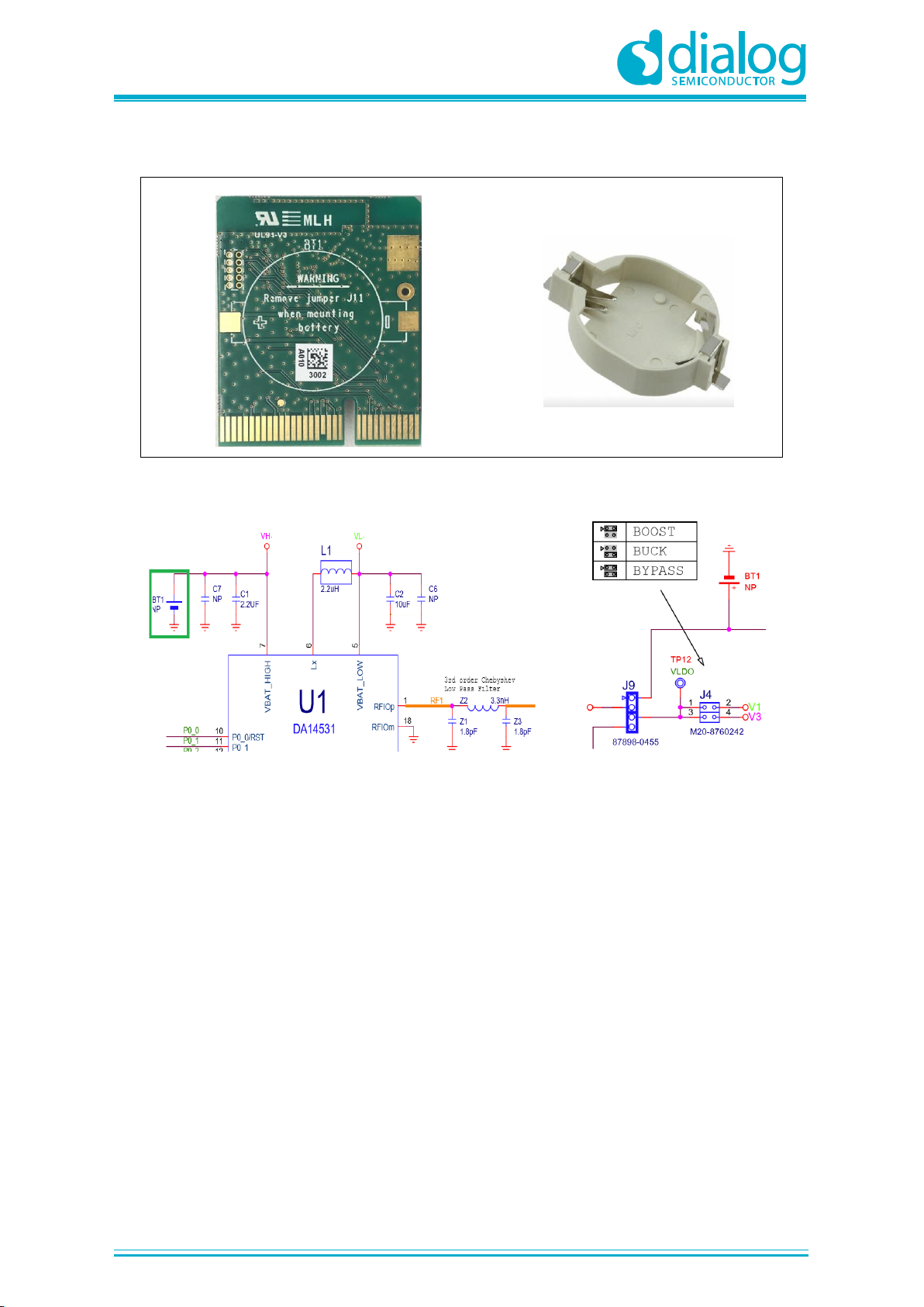
UM-B-114
DA14531 Development Kit Pro Hardware User Manual
User Manual
Revision 1.1
25-Oct-2019
CFR0012
38 of 80
© 2019 Dialog Semiconductor
When battery is mounted, power source from PRO-MB must be removed.
Figure 31: BT1 Position (Left). Battery Holder, BC2032-F1, to Be Soldered (Right)
Figure 32: DA14531 PRO-DB Schematic (Left). DA14531 PRO-MB, Header J4 Settings (Right)
6.1.1 Enabling Coin Cell Battery on DA14531 PRO-DB
To enable a coin cell battery on DA14531 PRO-DB, before powering on the DA14531 DK PRO,
make the following changes:
● On DA14531 PRO-DB:
○ Solder the battery socket on the solder side (BT1) by using BC2032-F1 (see Figure 31)
○ Insert a CR2032 coin cell battery
● On PRO-MB (see Figure 32, right)
○ Remove all jumpers from J4
○ Ensure that no battery is inserted in BT1
6.1.2 Enabling Coin Cell Battery on PRO-MB
To enable a coin cell battery on DA14531 PRO-MB, before powering on the DA14531 DK PRO,
make the following changes:
● On DA14531 PRO-DB: ensure that no battery is inserted in BT1 (see Figure 31)
● On PRO-MB (see Figure 32, right):
○ Remove the jumper on J9:1-2 and apply a jumper on J9:3-4

UM-B-114
DA14531 Development Kit Pro Hardware User Manual
User Manual
Revision 1.1
25-Oct-2019
CFR0012
39 of 80
© 2019 Dialog Semiconductor
○ Solder the battery socket on the solder side (BT1) by using BU2032SM-BT-GTR (see Figure
33)
○ Insert a CR2032 coin cell battery
Figure 33: BT1 Position on PRO-MB (Left). Battery Holder, BU2032SM-BT-GTR, to Be Soldered
(Right)

UM-B-114
DA14531 Development Kit Pro Hardware User Manual
User Manual
Revision 1.1
25-Oct-2019
CFR0012
40 of 80
© 2019 Dialog Semiconductor
7 First Steps with DA14531 DK PRO
The DA14531 DK PRO comes in with a pre-defined default configuration. However, due to the low
GPIO pin count, several functions are multiplexed and can be enabled as needed via jumpers. In the
default configuration, the DA14531 DK PRO supports the following functions:
● DA14531-FCGQFN24: reset, JTAG and SPI data flash. Single-wire UART is also supported with
proper jumper settings.
● DA14531-WLCSP17: reset, JTAG and SPI data flash
In the following sections, the supported features are detailed for each daughterboard.
7.1 Configuration of DA14531 DK PRO with a DA14531 FCGQFN24 PRO-DB
Figure 34: Default Setup of the DA14531 DK PRO with DA14531 FCGQFN24 PRO-DB

UM-B-114
DA14531 Development Kit Pro Hardware User Manual
User Manual
Revision 1.1
25-Oct-2019
CFR0012
41 of 80
© 2019 Dialog Semiconductor
In the DA14531 FCGQFN24 PRO-DB, the push button SW1 must be placed in the H position for
BUCK mode (Figure 34).
The DA14531 PRO-MB is delivered in a default configuration (Figure 34) which:
● Enables the on-board SPI data flash
● Enables the JTAG (SWD) debugging interface
● Enables single-wire UART by adding jumpers on J10:1 to J1:15 and J10:2 to J15:17 (marked by
blue)
● Enables the user push button SW2 and user LED D5
● Connects SW3 to SWDIO (JTAG interface) by removing the jumper
● Enables C-Trig. Please note that it is connected to the signal (P0_11) which drives SW2. If both
functionalities are required, assign one of the two functions to a free GPIO and wire accordingly.
● Allows the DA14531 to be reset (over JTAG or by using the SW1 push button)
● Sets DA14531 DCDC converter to Buck mode to provide 3.3 V
● Enables the current sensing circuit
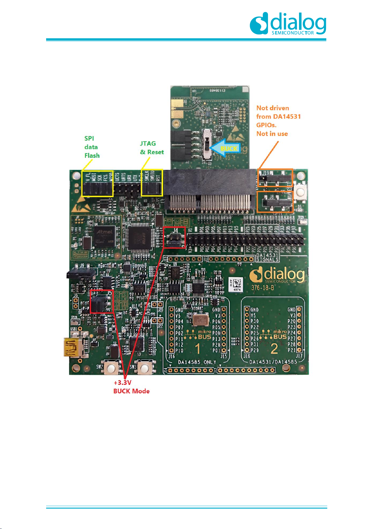
UM-B-114
DA14531 Development Kit Pro Hardware User Manual
User Manual
Revision 1.1
25-Oct-2019
CFR0012
42 of 80
© 2019 Dialog Semiconductor
7.2 Configuration of DA14531 DK PRO with a DA14531 WLCSP17 PRO-DB
Figure 35: Default Setup of the DA14531 DK PRO with a DA14531 WLCSP17 PRO-DB
In the DA14531 WLCSP17 PRO-DB, the push button SW1 must be placed in the H position for
BUCK mode (Figure 35).
The DA14531 PRO-MB is delivered in a default configuration (Figure 35) which:
● Enables the on-board SPI data flash
● Enables the JTAG (SWD) debugging interface
● Allows the DA14531 to be reset (over JTAG or by using the SW1 push button)
● Sets DA14531 DCDC converter to Buck mode to provide 3.3 V
● Enables the current sensing circuit
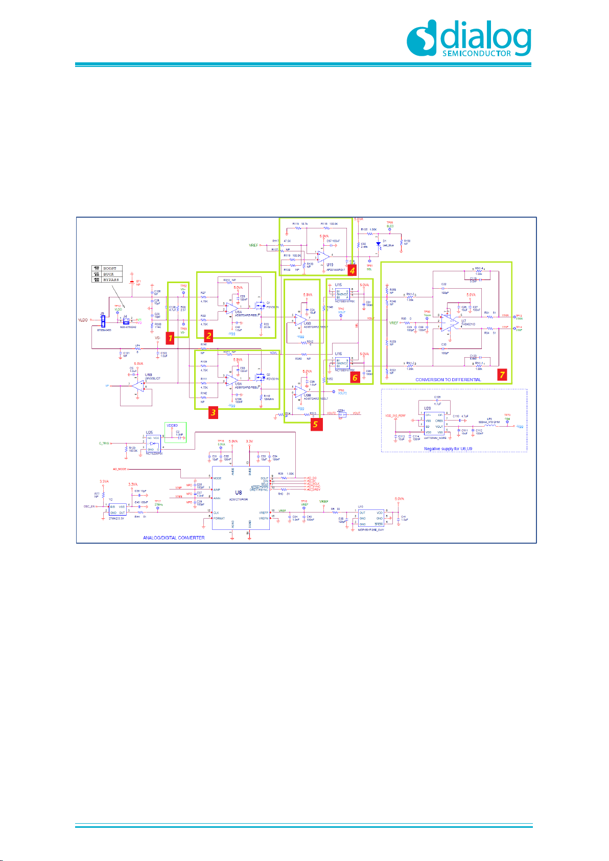
UM-B-114
DA14531 Development Kit Pro Hardware User Manual
User Manual
Revision 1.1
25-Oct-2019
CFR0012
43 of 80
© 2019 Dialog Semiconductor
8 Current Measurements
Current drawn from the DA14531 PRO-DB can be measured with a good accuracy by using the
current sensing circuit and the power profiler of Dialog’s SmartSnippets Toolbox.
In this section, the current measurement circuit as well as the setup and the measurements of the
power profiler are described, and the measurement accuracy is presented.
8.1 Current Measurement Circuit of PRO-MB
Figure 36: Current Measurement Circuit of DA14531 PRO-MB
Current measurement circuit is a section of the PRO-MB. The input to the circuit is the voltage across
the sense resistor (R28). The output is the differential pair VINP, VINN which are connected to the
inputs of the A/D converter.
The functional blocks of the current measurement circuit include:
● Sense resistor R28 (2.37 Ω)
● High scale C/V converter (Gain: 9.98 V/mA)
● Low scale C/V converter (Gain: 4989 V/mA)
● High/Low comparator: switches to high scale above ~300 μΑ and back to low scale below ~250
μA (with hysteresis)
● Voltage buffers. The V
SS
pin gets a -228 mV rail to allow the output to reach true zero
● Analog multiplexers: the low scale output is presented to the A/D converter with a negative
polarity
● Single-ended to differential converter: it converts the ground referenced input to a differential pair
aligned with the mid-scale reference voltage (V
REF
= 2.5 V) and a gain of ±0.5

UM-B-114
DA14531 Development Kit Pro Hardware User Manual
User Manual
Revision 1.1
25-Oct-2019
CFR0012
44 of 80
© 2019 Dialog Semiconductor
The differential amplifier outputs are connected to the ADC input. The digitally converted current
samples are sent to PC through the UART-to-USB IC (U12). Finally, the measured current is
presented to the PC converter and displayed in the power profiler of SmartSnippet Toolbox.
Figure 37: Current Measurement Presented in Power Profiler of SmartSnippets Toolbox
8.2 Power Profiler of Smartsnippet Toolbox
Dialog’s SmartSnippets Toolbox can be invoked from within the SmartSnippets Studio Welcome
page.
Alternately, it can run directly from the start menu under the section “Dialog SmartSnippets Studio
vx.x.xx\Dialog SmartSnippets Toolbox for SmartSnippets Studio vx.x.xx”.
Upon opening, the application starts with the settings/interface options page. An existing entry can be
selected from the list, or a new configuration can be created by pressing the “New” button (Figure
38).
At this point, to change the hardware setup, for example, to plug in another board, by pressing the
“Refresh” button (Figure 38), the list of available ports will be updated.
To select the chip version, when the “Detect” button (Figure 38) is pressed, the tool identifies the
exact part number of the SoC on the target board
For power measurements, users need to select an interface that allows the PC software
(SmartSnippets Toolbox) to communicate with the A/D converter through the correct SPI port (which
is camouflaged in the PC as a plain UART part. In Figure 38, the selected SPI port is COM18).
For power measurement, the “UART/SPI” option in Figure 38 is preferred, because JTAG is used for
downloading code from the IDE and debugging. The “Hybrid” option can also be used. But power
measurements are not feasible in the “UART-only” or “JTAG” option.

UM-B-114
DA14531 Development Kit Pro Hardware User Manual
User Manual
Revision 1.1
25-Oct-2019
CFR0012
45 of 80
© 2019 Dialog Semiconductor
Figure 38: SmartSnippets Toolbox Configuration
In “Hybrid” mode (Figure 39), the selection box automatically lists the only valid SPI/COM ports and
debugger serial numbers.
Figure 39: Hybrid Configuration
8.3 Power Profiler Setup
After selecting the proper option (UART/SPI or Hybrid) in Figure 38, press “Open” and the main
window of the Power Profiler application in SmartSnippets Toolbox will pop up (Figure 40). Press
“Config” button in the bottom right and check if everything is configured correctly (Figure 41).
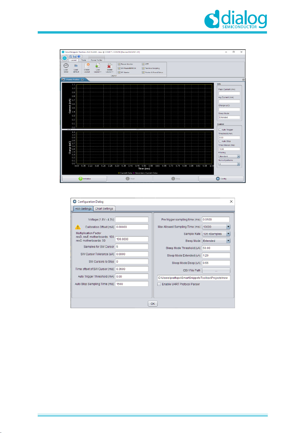
UM-B-114
DA14531 Development Kit Pro Hardware User Manual
User Manual
Revision 1.1
25-Oct-2019
CFR0012
46 of 80
© 2019 Dialog Semiconductor
Figure 40: Power Profiler of SmartSnippets Toolbox Main Window
Figure 41: Power Profiler Configuration
In a new profile, the “Voltage” box in the “H/W Settings” is typically empty and the “Calibration
Offset” is zero. Apply the correct voltage as configured in the PRO-MB LDO (typically, it is 3.3 V).
The calibration offset (mA) will be filled automatically with a calculated value. This value is good
enough for measuring with ±2% accuracy, so in most cases we can leave it as is.
Check the multiplication factor. For DA14531 it should be 100.
Optionally, set a max scale for the waveform window, because typically there are large peaks on
wake-up from sleep (charging capacitors), so the useful part of the signal is compressed to a very
small area. To set a max scale for the waveform window, access the “Chart Settings” tab (Figure
42) and set the max scale of “Current1” to 10 mA. Note that this does not affect in any way the
accuracy of measurement. It only zooms-in the waveform that is presented on the viewer window.
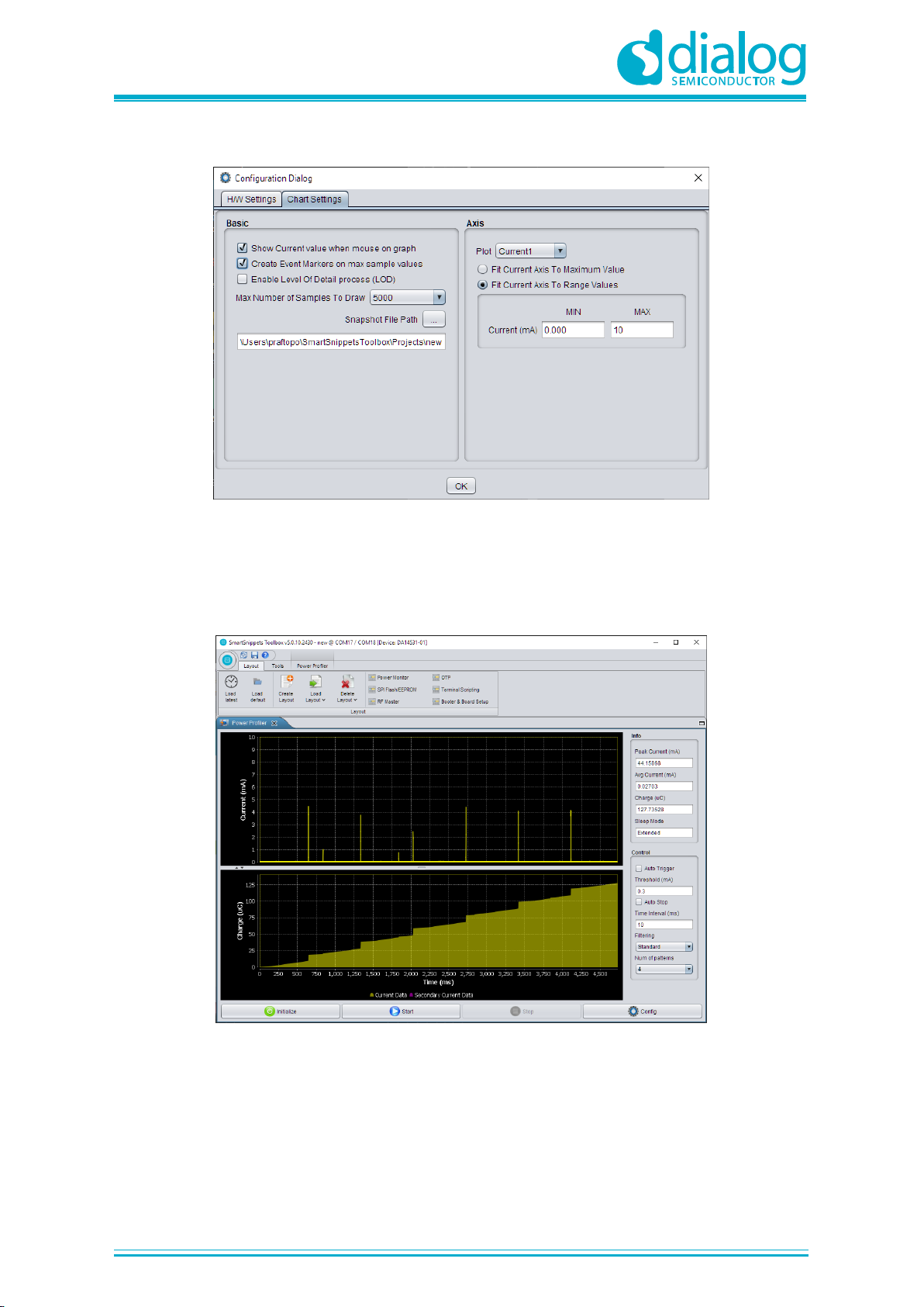
UM-B-114
DA14531 Development Kit Pro Hardware User Manual
User Manual
Revision 1.1
25-Oct-2019
CFR0012
47 of 80
© 2019 Dialog Semiconductor
Press “OK” and return to the measurement window.
Figure 42: Power Profiler Chart Settings
8.4 Measurements
In the measurement window (Figure 43), press “Initialize” on the bottom left (this step is only needed
at the first communication with the A/D converter) and then press “Start”.
Figure 43: Free Running Capture
A triggered capture can be used for acquiring a single waveform (Figure 44).

UM-B-114
DA14531 Development Kit Pro Hardware User Manual
User Manual
Revision 1.1
25-Oct-2019
CFR0012
48 of 80
© 2019 Dialog Semiconductor
Figure 44: Triggered Capture
Figure 45 shows a combination of the main Current1/Oscilloscope. This option can be selected from
the “Power Profiler” tab. The top window presents the free running waveform, while the bottom
window uses the trigger and time interval values to capture and print up to 10 of the most recent
waveforms in an oscilloscope fashion. Note that the “Auto Trigger” and “Auto Stop” checkboxes
under “Control” on the lower right-hand side must remain unchecked.
Figure 45: Oscilloscope Option

UM-B-114
DA14531 Development Kit Pro Hardware User Manual
User Manual
Revision 1.1
25-Oct-2019
CFR0012
49 of 80
© 2019 Dialog Semiconductor
8.5 Power Profiler Software Cursors
Users can insert a vertical cursor (SW cursor) in the Power Profiler display by toggling C-Trig
(mapped to P0_11 of DA14531) in the SW running on the ARM Cortex M0+ CPU.
The SW cursor provides an accurate correlation between the SW and the power profile of the system
in real time. The vertical line is not movable on the display window.
Figure 46: Power Profiler Software Cursors
8.6 Manual Calibration
For an ultimate measurement accuracy, it is necessary to perform a manual calibration by following
the step below:
1. Remove the daughter board, that is, the load, by physically disconnecting the PRO-DB from the
motherboard or temporarily removing the jumper from the connector J4.
2. In the main window of the Power Profiler, press “Config” and temporarily set the calibration offset
to zero (Figure 47).
Figure 47: Setting Offset to Zero

UM-B-114
DA14531 Development Kit Pro Hardware User Manual
User Manual
Revision 1.1
25-Oct-2019
CFR0012
50 of 80
© 2019 Dialog Semiconductor
3. Run a free running capture for a few seconds and note down the number in the “Avg Current
(mA)” box (Figure 48). Note that the last digits of the number keep changing slowly due to
temperature drift. It is important to periodically execute the calibration steps.
Figure 48: Measuring Offset
4. Finally, put this average value with a negative sign in the “Calibration Offset (mA)” box. CTRL-C
and CTRL-V also works.
Figure 49: Setting Calibration Offset
5. Re-insert the daughterboard or restore the jumper removed from J4 in the previous step.
NOTE
Please notice that the value in the Voltage box is 3 V. This is a typical value used across the industry for
comparing BLE power measurements. Therefore, the power configuration on DA14531 PRO-MB must be
updated accordingly (J5: 2-4).
UM-B-114
DA14531 Development Kit Pro Hardware User Manual
User Manual
Revision 1.1
25-Oct-2019
CFR0012
51 of 80
© 2019 Dialog Semiconductor
8.7 Accuracy of Current Measurement Circuit
The measuring range of the current measurement circuit in DA14531 PRO-MB is 1 μΑ to 240 mA.
The circuit accuracy is measured by applying a constant current, monitoring the output with the
SmartSnippets Toolbox, and compare the outcome.
In general, the inaccuracy presented in the current measurement circuit is less than 5% (practically
less than 2%) in most of the current range. There are two areas where the inaccuracy is of the order
of 10%, that is, from 1 μA to 10 μA and from 100 μΑ to 300 μΑ (Table 17).
Table 17: Accuracy of the Current Measurement Circuit
Current Range
Inaccuracy (%)
1 μΑ to 10 μΑ
<13%
10 μA to 100 μA
<5%
100 μA to 300 μA
<10%
300 μA to 240 mA
<5%
Figure 50: Current Measurement Circuit Response, Indicative Graph
1.E-06
1.E-05
1.E-04
1.E-03
1.E-02
1.E-01
1.E-06 1.E-05 1.E-04 1.E-03 1.E-02 1.E-01
measured current (A)
input current (A)
1.1V boost
1.8V buck
3.3V buck

UM-B-114
DA14531 Development Kit Pro Hardware User Manual
User Manual
Revision 1.1
25-Oct-2019
CFR0012
52 of 80
© 2019 Dialog Semiconductor
Figure 51: Current Measurement Circuit Inaccuracy, Indicative Graph
-30
-20
-10
0
10
20
30
1.E-06 1.E-05 1.E-04 1.E-03 1.E-02 1.E-01
error (%)
input current (A)
1.1V boost
1.8V buck
3.3V buck

UM-B-114
DA14531 Development Kit Pro Hardware User Manual
User Manual
Revision 1.1
25-Oct-2019
CFR0012
53 of 80
© 2019 Dialog Semiconductor
9 Known Issues
9.1 Switching Transient Artifacts of Current Measurement Circuit
When the current measurement circuit changes scale, it presents some small or large voltage step
on the A/D converter inputs. An ideal converter (infinite bandwidth) would produce a single spike at
the point of switching. But since the converter is not ideal, it produces a ringing like waveform (Figure
52).
Figure 52: A/D Converter Distortions
In Figure 52 we can identify three types of ringing artifacts created by the A/D converter:
● Switching from low to high scale (1)
● Not switching, but instead a signal with very steep fall is present (2)
● Switching from high to low scale and then another switch Low-High-Low creates this exaggerated
false peak (due to a large difference of the DC levels of the two C/V converters, 3)
9.2 Push Button SW3
SW3 is enabled on DA145xx DEVKT-P PRO-MB by P1_1. By default, this signal is not driven from
DA14531. Consequently, jumper J19:4-5 is not required in DA14531 DK PRO.
Figure 53: Disable SW3. Remove Jumper from J19:4-5
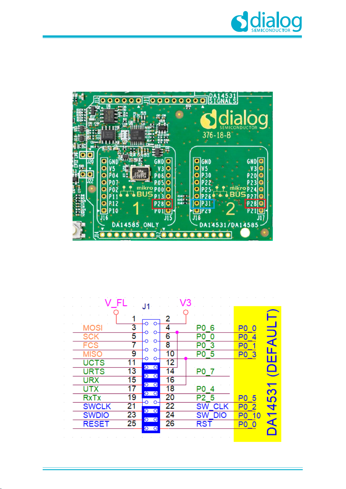
UM-B-114
DA14531 Development Kit Pro Hardware User Manual
User Manual
Revision 1.1
25-Oct-2019
CFR0012
54 of 80
© 2019 Dialog Semiconductor
9.3 mikroBUS Wrong Label
The label of pin 2 for headers J15 and J17 is wrong. This pin is connected to P3_0 and not to P2_8.
The label of pin 2 for J18 is wrong. There is a label of P31 but the pin is not connected.
Figure 54: mikroBUS Wrong Label
9.4 4-Wire UART Special Considerations
When the 4-wire UART functionality is used with DA14531 Pro-DB and the reset function is enabled
on P0_0, the chip will not boot and still remain in the reset state.
Figure 55: Full UART Configuration - CTS Issue

UM-B-114
DA14531 Development Kit Pro Hardware User Manual
User Manual
Revision 1.1
25-Oct-2019
CFR0012
55 of 80
© 2019 Dialog Semiconductor
As shown in Figure 55, the UCTS signal is shorted to P0_0 when a DA14531 PRO-DB is used. This
has been done to maintain compatibility with DA14585 daughterboards. The UCTS signal is an input
to the DA14531 and is driven high from the motherboard side (MB_RTS). If P0_0 is configured as
reset (active high), the motherboard will keep the DA14531 in reset indefinitely and prevent it from
booting (the Booter defaults this pin to the reset function between boot steps). To avoid this problem
there are several options:
● Disconnect the UCTS jumper and place it after the device has booted and P0_0 has been
configured properly by the firmware for the UCTS function
● Assign UCTS to another free GPIO and wire it accordingly

UM-B-114
DA14531 Development Kit Pro Hardware User Manual
User Manual
Revision 1.1
25-Oct-2019
CFR0012
56 of 80
© 2019 Dialog Semiconductor
Appendix A FCGQFN24 PRO-DB: DA14531-00FXDB-P_(376-04-F2)
A.1 Schematic
Figure 56: Schematic, FCGQFN24, DA14531-00FXDB-P_(376-04-F2)
SWDIO
SWCLK
C6
NP
C7
NP
Title :
Doc. Nr. Rev :
Date: Sheet: of
Dialog Semiconductor
N.E.O. Athinon- Patron 15
26441, Patra, Greece
tel. (+30) 2610390940
fax. (+30) 2610390941
Designer: F
DA14531/D2632 Development Kit Daughterboard
2 2Monday, August 12, 2019
Kalliopi Liantinioti
<Variant Name>
MB0_6
MB0_5
MB0_4
MB0_3
MB0_0
MB0_7
R14 0
BT1
NP
MB0_5
R23 NP
R24 NP
MB2_1
MB2_0
MB0_6
VBAT
MB2_0
MB1_0
MB1_1
MB2_3
MB2_2
MB2_1
MB2_6
MB2_5
MB2_4
MB2_9
MB2_8
MB2_7
MB3_0
L1
2.2uH
Z2 3.3nH
Z3
1.8pF
Z1
1.8pF
R32 NP
MB3_1
JTAG
BREAKOUT
HEADERS
4-PIN UART
SPI
FLASH
Y1
32.0000MHZ
1 3
2 4
MB2_3
MB2_4
R31 0
R15 NP
Z4
1.00pF
Z6
0.5pF
MB2_2
MB2_5
MB0_0
MB0_3
SWCLK
SWDIO
MB0_6
MB0_5
MB0_4
J1A
PCIE_64
A1A1A6
A6
B9
B9
B10
B10
B13
B13
B14
B14
A24
A24
B28
B28
B30
B30
A10
A10
A11
A11
A12
A12
B32
B32
A14
A14
A15
A15
A16
A16
A17
A17
A18
A18
A19
A19
A20
A20
A21
A21
A22
A22
B17
B17B1B1
A25
A25
B20
B20
B16
B16
B11
B11
B31
B31
B24
B24
A31
A31
A32
A32
MB1_3
MB0_7
J1B
PCIE_64
B15
B15
A28
A28
B3
B3
B18
B18
B22
B22
B19
B19
A27
A27
B26
B26
B12
B12B4B4
B5
B5A5A5
B6
B6B7B7
A7
A7A8A8
A9
A9
B25
B25
A26
A26
B27
B27
A29
A29A4A4
B8
B8
A13
A13
A23
A23
B23
B23
B29
B29
A30
A30
B2B2A2
A2
A3
A3
B21
B21
J2
M20-8890545R
DA14531
24-pin FCGQFN
U1
DA14531-QFN24
XTAL32Mm
4
RFIOm
18
RFIOp
1
GND_DC DC
21
XTAL32Mp
3
P0_8
17
P0_111P0_0/RST10P0_2/SWCLK
12
P0_3/XTAL32kp
13
P0_11
8
GND
20
GNDRF 2
2
P0_4/XTAL32km
14
P0_5
24
P0_10/SWDIO
9
P0_7
15
P0_6
22
Lx
6
VBAT_LOW
5
VSS
23
VBAT_HIGH
7
GNDRF 1
19
P0_9
16
R35 NP
R34 NP
UTX
VL+
URTS
UCTS
URX
VL-
VH+VH-
P0_0
R19 0
R20 0
R21 0
R22 0
MB2_4
MB2_3
MB2_1
MB2_0
RF2
RESET
Card Edge Connector (PCI-E)
1-WIRE UART(2)
MISO
CS#
MOSI
VBAT
SCLK
VH+
VL+
VH-
VH- VL-
R25 NP
R26 NP
MB0_4
(default)
(opt.1)
MB2_0MB0_5
R27 NP
R28 NP
MB0_5
R29 NP
P0_5
VL-
P0_10
P0_1
Z5 5.6nH
Y2
32.768KHZ
VH+
R33
NP
U2
TCR2EF11_LM_CT
IN
1
GND
2
CE
3
NC
4
OUT
5
P0_3
P0_4
VIN
VLDO
C2
10uF
CURRENT
MEASUREMENT
Z9 10pF
1.1V LDO
J3
NP_142-0761-861
1
234
Z7
NP
RF3
P0_2
P0_1
R11 NP
C3
1.0uF
APPLICABLE ONLY TO
DA14580DEVKT-P_B/C
FOR DA145xxDEVKT-P_D SET
TO BUCK (H) AND SELECT THE
DESIRED MODE FROM THE MB
P0_7
P0_6
P0_5
P0_9
P0_8
P0_11
P0_10
C4
1.0uF
SWDIO
SWCLK
DEBUGGING OPTION (NOT POPULATED)
C1
2.2UF
J5
Jtag_Conn_2x5_1mm27
VDD
7
DIO
4
CLK
3
URX
2
UTX
1
RST
6
VPP
5
GND1
8
NC1
9
GND2
10
VBAT
C5
NP
3rd order Chebyshev
Low Pass Filter
RF1
BYPASS
BOOST
SW1
JS203011JCQN
4
3
2 6
7
8
1 5
VL+
VIN
VBAT
VH+
VLDO
POWER MODE SELECTION
BUCK
(L)
(B)
(H)
ANT1
Antenna_IFA_ty pe_Right
MB2_1
MB2_0
MB2_7
MB2_6
MB2_5
MB2_4
MB2_3
MB2_2
MB2_9
MB2_8
MB3_0
MB3_1
VL+
R30 1.00k
P0_0
RST
R1 36
P0_0
R2 36
R3 36
P0_1
P0_2
R4 36
P0_3
R5 36
P0_4
R6 36
MISC. PERIPHERALS
RESET
MB1_3
MB1_1
MB1_0
P0_5
R7 36
R17 1.00k
R13 NP
P0_6
R8 36
R16 0
R18 1.00k
MB2_8
P0_7
R9 36
LED
POR
MB3_1
MB3_0
MB2_9
P0_8
R10 36
TRIG
BUTTON
P0_9
P0_10
R12 36
P0_11
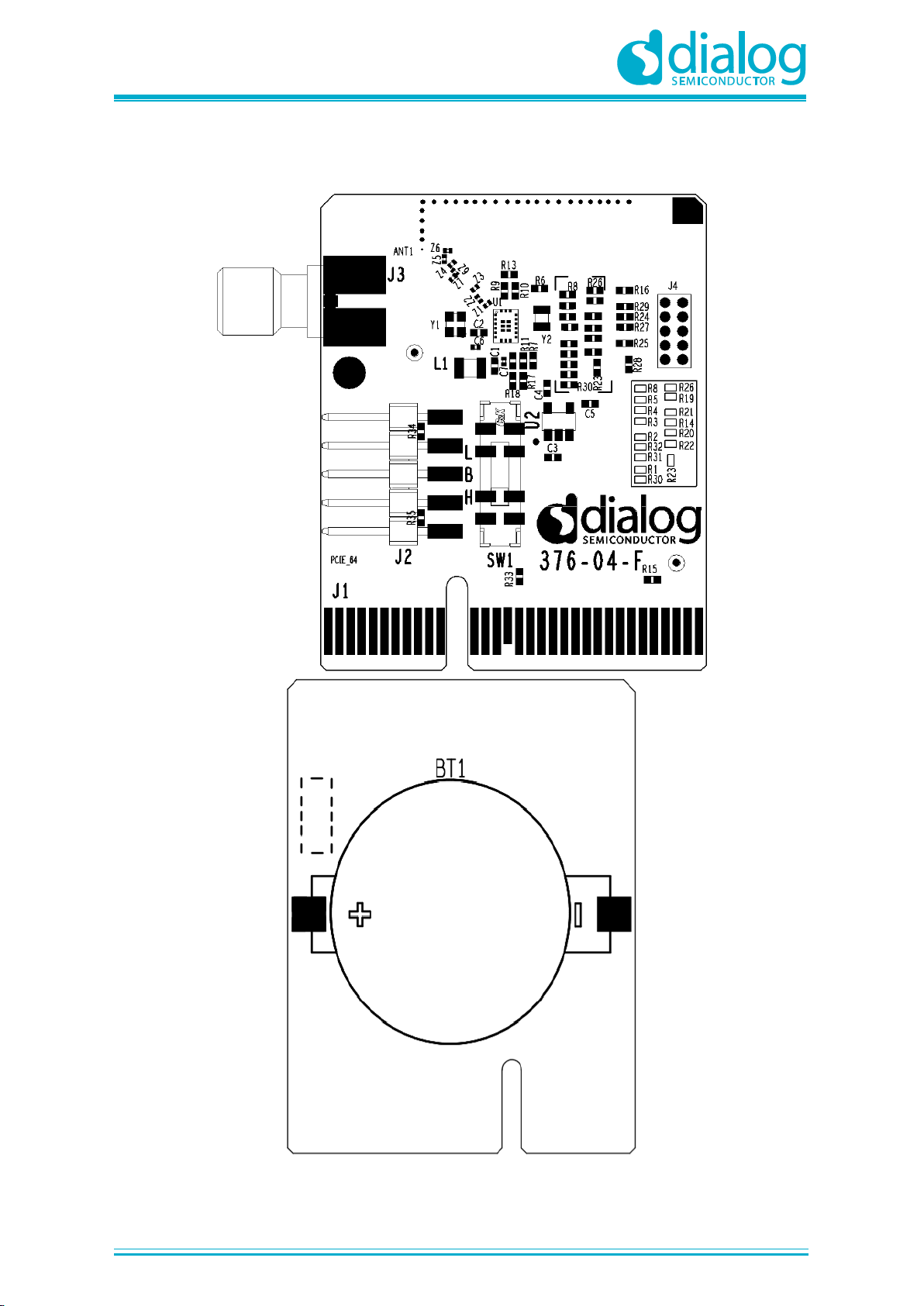
UM-B-114
DA14531 Development Kit Pro Hardware User Manual
User Manual
Revision 1.1
25-Oct-2019
CFR0012
57 of 80
© 2019 Dialog Semiconductor
A.2 Components Placement
Figure 57: Components on Top and Bottom Sides for FCGQFN24, DA14531-00FXDB-P_(376-
04-F2)
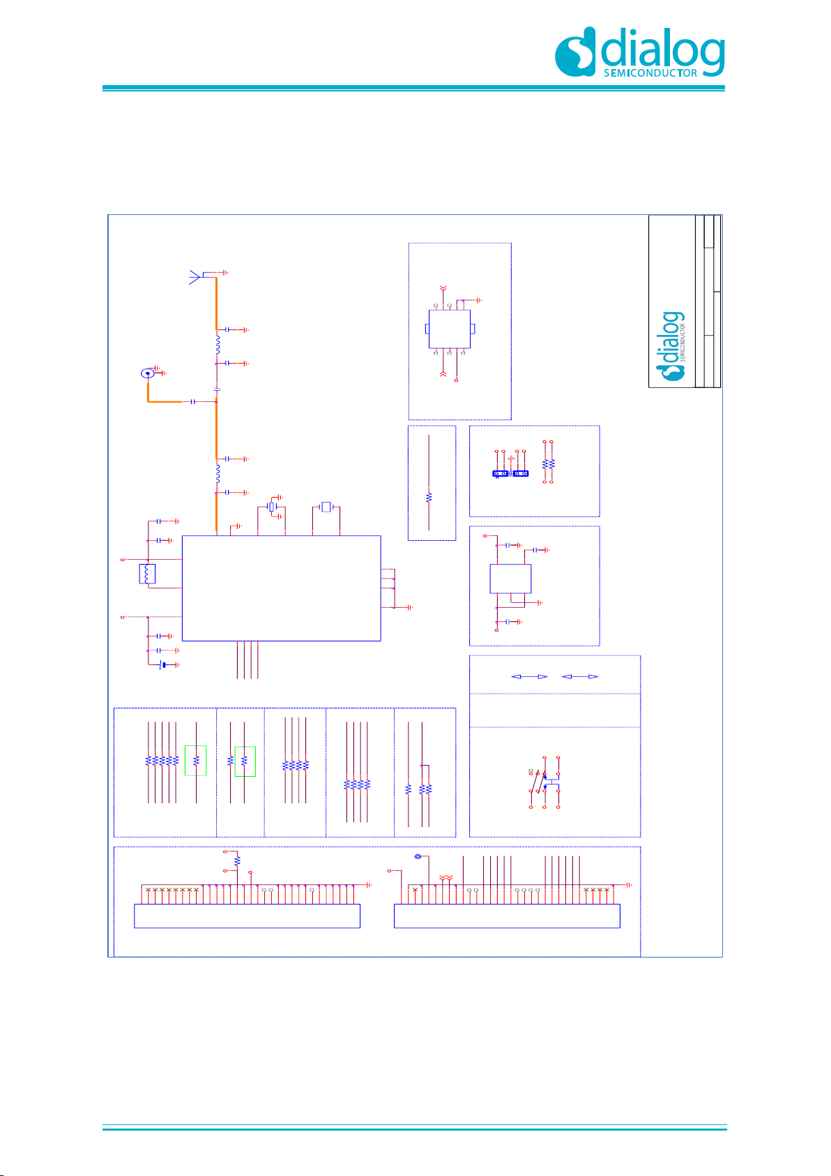
UM-B-114
DA14531 Development Kit Pro Hardware User Manual
User Manual
Revision 1.1
25-Oct-2019
CFR0012
58 of 80
© 2019 Dialog Semiconductor
Appendix B WLCSP17 PRO-DB: DA14531-00OGDB-P_(376-05-E)
B.1 Schematic
Figure 58: Schematic, WLCSP17, DA14531-00OGDB-P_(376-05-E)
SWDIO
SWCLK
MB0_6
MB0_5
MB0_4
MB0_3
MB0_0
MB0_7
R30 1.00K
BYPASS
BOOST
R14 0
BT1
NP_BC2032-F1
MB0_5 MB2_1
MB2_0
MB0_6
VBAT
MB2_0
MB2_3
MB2_2
MB2_1
MB2_5
MB2_4
SW1
JS203011JCQN
4
3
2 6
7
8
1 5
R33
NP
VH+
JTAG
BREAKOUT
HEADERS
4-PIN UART
SPI
FLASH
MB2_3
MB2_4
TP1
RST
MB2_2
MB0_0
R15 36
MB0_3
SWCLK
SWDIO
MB0_6
MB0_5
MB0_4
J1A
PCIE_64
A1
A1
A6
A6
B9
B9
B10
B10
B13
B13
B14
B14
A24
A24
B28
B28
B30
B30
A10
A10
A11
A11
A12
A12
B32
B32
A14
A14
A15
A15
A16
A16
A17
A17
A18
A18
A19
A19
A20
A20
A21
A21
A22
A22
B17
B17
B1
B1
A25
A25
B20
B20
B16
B16
B11
B11
B31
B31
B24
B24
A31
A31
A32
A32
MB0_7
J1B
PCIE_64
B15
B15
A28
A28
B3
B3
B18
B18
B22
B22
B19
B19
A27
A27
B26
B26
B12
B12
B4
B4
B5
B5
A5
A5
B6
B6
B7
B7
A7
A7
A8
A8
A9
A9
B25
B25
A26
A26
B27
B27
A29
A29
A4
A4
B8
B8
A13
A13
A23
A23
B23
B23
B29
B29
A30
A30
B2
B2
A2
A2
A3
A3
B21
B21
J2
M20-8890545R
P0_5
DA14531
17-ball WLCSP
U1
DA14531-WLCSP17
XTAL32Mm
E1
RFIOm
A3
RFIOp
A1
GND_DC DC
F2
XTAL32Mp
D2
P0_1
E5
P0_0/RST
F4
P0_2/SWCLK
C5
P0_3/XTAL32kp
B4
GND_RF 2
C1
P0_4/XTAL32km
A5
P0_5/SWDIO
D4
Lx
G3
VBAT_LOW
G1
VSS
E3
VBAT_HIGH
G5
GND_RF 1
C3
UTX
URTS
UCTS
URX
P0_0
Title :
Doc. Nr. Rev :
Date: Sheet: of
Dialog Semiconductor
N.E.O. Athinon- Patron 15
26441, Patra, Greece
tel. (+30) 2610390940
fax. (+30) 2610390941
Designer:376-05-E E
DA14531/D2632 Development Kit Daughterboard
2 2Friday , August 09, 2019
PR
<Variant Name>
Y1
32.0000MHZ
1 3
2 4
MB2_4
MB2_3
MB2_1
MB2_0
RESET
Card Edge Connector (PCI-E)
1-WIRE UART(2)
MISO
CS#
MOSI
VBAT
SCLK
VH+
VL+
VH-
VH- VL-
VL+
MB0_4
(default)
(opt.1)
MB2_0MB0_5
MB0_5
P0_5
VL-
C2
10uF
C1
2.2UF
L1
2.2uH
P0_3
P0_4
SWDIO
SWCLK
DEBUGGING OPTION (NOT POPULATED)
J5
Jtag_Conn_2x5_1mm27
VDD
7
DIO
4
CLK
3
URX
2
UTX
1
RST
6
VPP
5
GND1
8
NC1
9
GND2
10
VBAT
U2
TCR2EF11_LM_CT
IN
1
GND
2
CE
3
NC
4
OUT
5
VBAT
VIN
VIN
VLDO
VLDO
VH+
BUCK
POWER MODE SELECTION
DEFAULT BYPASS (B)
CURRENT
MEASUREMENT
Z1
1.8pF
Z2 3.3nH
Z3
1.8pF
3rd order Chebyshev
Low Pass Filter
RF1
Z7
NP
Z9 10pF
RF3
1.1V LDO
Z4
1.00pF
Z6
0.5pF
Z5 5.6nH
C6
NP
C7
NP
J3
NP_142-0761-861
1
234
P0_2
P0_1
R35 NP
R34 NP
VL-VL+
VH- VH+
C3
1.0uF
P0_5
C4
1.0uF
C5
NP
(H)
(L)
(B)
ANT1
Antenna_IFA_ty pe_Right
RF2
MB2_1
MB2_0
MB2_5
MB2_4
MB2_3
MB2_2
R1 36
R2 36
R3 36
R4 36
R5 36
R6 NP
VL+
R23 NP
R25 NP
R24 NP
R26 NP
R27 NP
R28 NP
R29 NP
P0_0
RST
P0_0
R19 0
R21 0
R20 0
P0_1
R22 0
P0_2
P0_3
P0_4
Y2
NP_32.768KHZ
MISC. PERIPHERALS
RESET
P0_5

UM-B-114
DA14531 Development Kit Pro Hardware User Manual
User Manual
Revision 1.1
25-Oct-2019
CFR0012
59 of 80
© 2019 Dialog Semiconductor
B.2 Components Placement
Figure 59: Components on Top and Bottom Sides for WLCSP17, DA14531-00OGDB-P_(376-05-
E)
UM-B-114
DA14531 Development Kit Pro Hardware User Manual
User Manual
Revision 1.1
25-Oct-2019
CFR0012
60 of 80
© 2019 Dialog Semiconductor
Appendix C PRO-MB
C.1 Schematic
Figure 60: DA14531 PRO-MB, headers and connectors
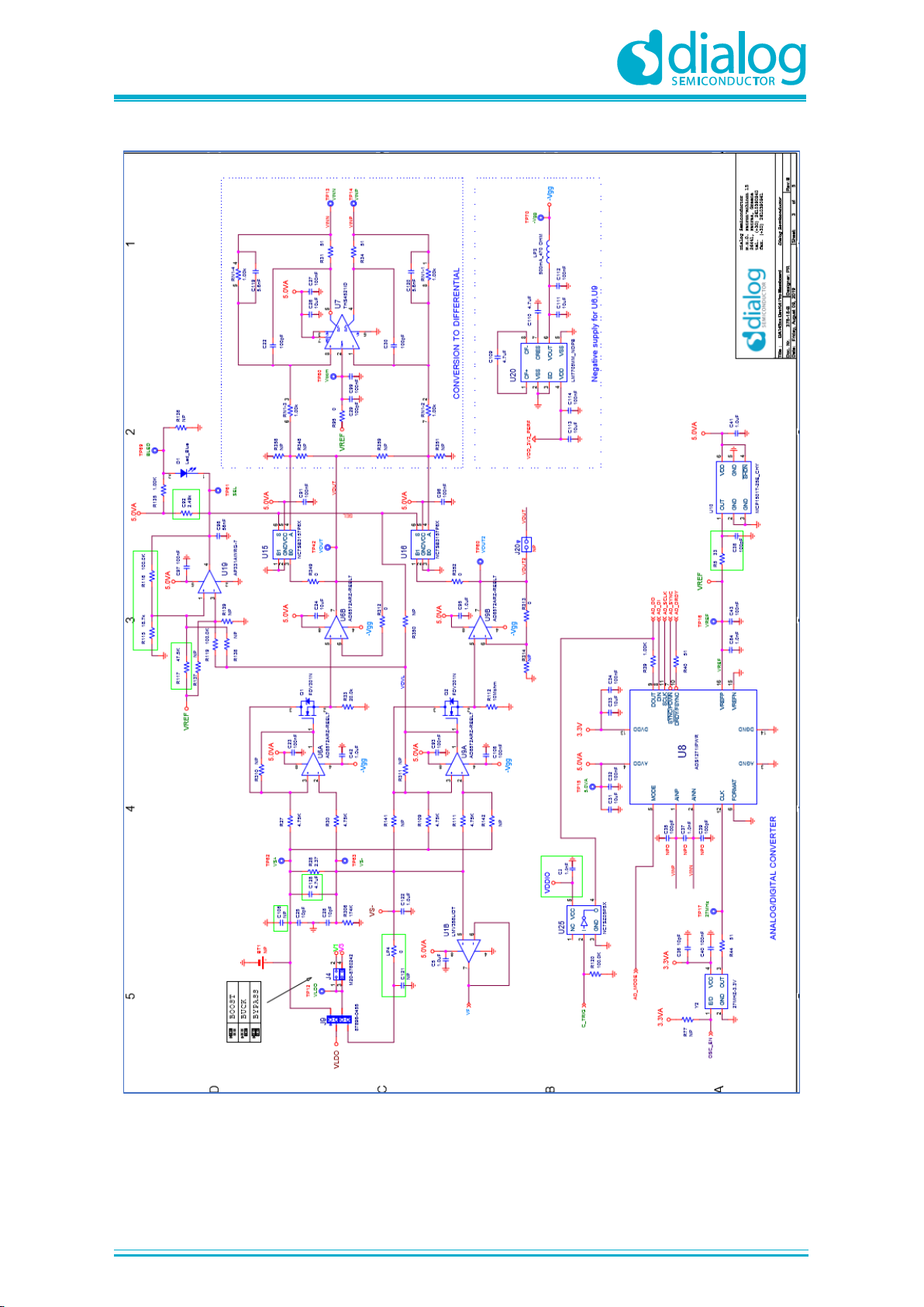
UM-B-114
DA14531 Development Kit Pro Hardware User Manual
User Manual
Revision 1.1
25-Oct-2019
CFR0012
61 of 80
© 2019 Dialog Semiconductor
Figure 61: DA14531 PRO-MB, Current Measurement Circuit
UM-B-114
DA14531 Development Kit Pro Hardware User Manual
User Manual
Revision 1.1
25-Oct-2019
CFR0012
62 of 80
© 2019 Dialog Semiconductor
Figure 62: DA14531 PRO-MB, JTAG MCU
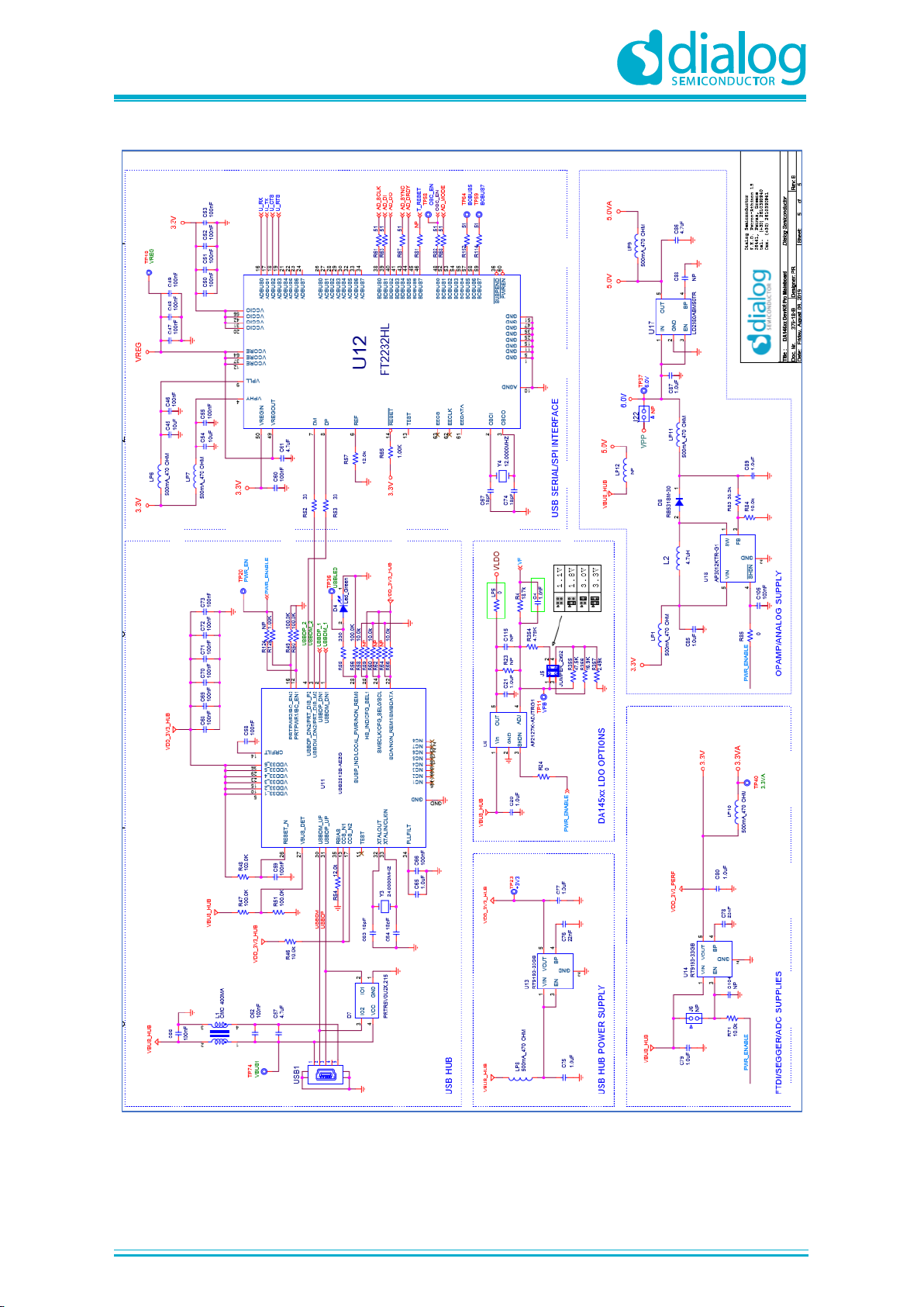
UM-B-114
DA14531 Development Kit Pro Hardware User Manual
User Manual
Revision 1.1
25-Oct-2019
CFR0012
63 of 80
© 2019 Dialog Semiconductor
Figure 63: DA14531 PRO-MB, USB Hub, USB to UART IC, and Power Section

UM-B-114
DA14531 Development Kit Pro Hardware User Manual
User Manual
Revision 1.1
25-Oct-2019
CFR0012
64 of 80
© 2019 Dialog Semiconductor
C.2 Components Placement
Figure 64: Components on Top Side of DA14531 PRO-MB
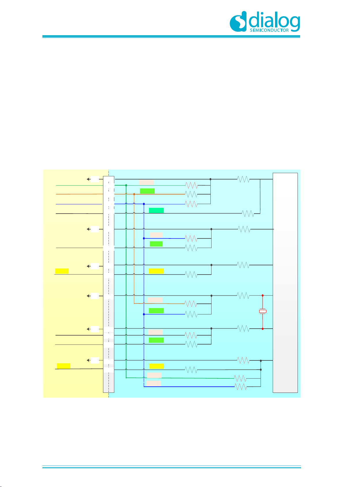
UM-B-114
DA14531 Development Kit Pro Hardware User Manual
User Manual
Revision 1.1
25-Oct-2019
CFR0012
65 of 80
© 2019 Dialog Semiconductor
Appendix D Detailed Description of Hardware Setup
D.1 DA14531 WLCSP17 PRO-DB, GPIOs Configuration, and R-matrix
D14531 WLCSP PRO-DB provides six pins. To serve all the available functions, a resistor matrix (RMatrix) is applied to DA14531 WLCSP PRO-DB.
Signal multiplication is completed with signal selection header (J1) on PRO-MB.
Functions available for DA14531 WLCSP17 PRO-DB are the SPI data bus, JTAG, Reset, UART, and
XTAL32K.
The default setup for the D14531 WLCSP17 PRO-DB is: Reset, JTAG, and SPI data bus (assigned
to SPI data flash).
Figure 65 and Table 18 show the resistor matrix for DA14531 WLCSP17 PRO-DB.
DA14531
WLCSP
P0_0
P0_1
P0_2
P0_3
P0_4
MB2_0
R1 = 36
MB0_4
R23 = NP
MB0_6
R22 = 0
MB0_5
R27 = NP
MB2_1
R2 = 36
MB0_5
R24 = NP
MB0_3
R20 = 0
MB2_2
R3 = 36
SWCLK
R14 = 0
MB2_3
R4 = 36
MB0_6
R25 = NP
MB0_5
R21 = 0
MB2_4
R5 = 36
MB0_7
R26 = NP
MB0_0
R19 = 0
RESET
R30 = 1K
P0_5
MB2_5
R6 = Not pop
MB0_4
R28 = NP
MB0_5
R29 = NP
SWDIO
R15 = 36
Y2
32.768 KHz
NP
UTX
URX
MISO
MOSI
UCTS
/CS
SCK
URTS
URX
UTX
SWCLK
SWDIO
P2_0
P2_1
P2_2
P2_3
P2_4
P2_5
P0_4
P0_6
P0_5
B6
A4
B8
B22
A7
A8
B7
A13
A27
A23
B23
B29
B26
B4
A9
P0_7
P0_0
P0_3
RST
PRO Motherboard
531_WLCSP PRO
daughterboard
Signals Naming
On PRO-Motherboard
Figure 65: System Configuration for DA14531 DK PRO with a DA14531 WLCSP17 PRO-DB
(Default)

UM-B-114
DA14531 Development Kit Pro Hardware User Manual
User Manual
Revision 1.1
25-Oct-2019
CFR0012
66 of 80
© 2019 Dialog Semiconductor
Table 18: DA4531 WLCSP17 PRO-DB Default Setup
DA14531 WLCSP17 PRO-DB Pin Connectivity
Interfaces
Signals
P0_0
P0_1
P0_2
P0_3
P0_4
P0_5
PRO-MB signals
P2_0
R1 P2_1
R2
P2_2
R3
P2_3
R4
P2_4
R5 P2_5
R6
UART
UTX
R23
R28
URX
R27
R24 R29
URTS
R26
UCTS
R25
SPI Data Flash
MOSI
R22
MISO
R21
SCS
R20
SCL
R19
JTAG
SWCLK
R14 SWDIO
R15
XTAL32K
XT32Kp
Y2
XT32Km
Y2
Other
Reset
R30
D.2 DA14531 FCGQFN24 PRO-DB, GPIOs Configuration, and R-matrix
DA14531 FCGQFN24 PRO-DB provides 12 pins. To serve all the available functions, a resistor
matrix (R-Matrix) is applied to DA14531 FCGQFN24 PRO-DB.
Signal multiplication is completed with the signal selection headers (J1, J8, and J19) on PRO-MB.
Functions available for DA14531 FCGQFN24 PRO-DB are the SPI data bus, JTAG, Reset, UART,
XTAL32K, LED, Key, and extension ports (mikroBUS and Arduino).
The default setup for the D14531 FCGQFN24 PRO-DB is: Reset, JTAG, and SPI data bus (assigned
to SPI data flash), single-wire UART, LED and a Key. Extension ports use multiplexed signals.
Figure 66 and Table 19 show the resistor matrix for FCGQFN24.

UM-B-114
DA14531 Development Kit Pro Hardware User Manual
User Manual
Revision 1.1
25-Oct-2019
CFR0012
67 of 80
© 2019 Dialog Semiconductor
DA14531
FCGQFN24
P0_0
P0_1
P0_2
P0_3
P0_4
MB2_0
R1 = 36
MB0_4
R23 = NP
MB0_6
R22 = 0
MB0_5
R27 =NP
MB2_1
R2 = 36
MB0_5
R24 = NP
MB0_3
R20 = 0
MB2_2
R3 = 36
SWCLK
R14 = 0
MB2_3
R4 = 36
MB0_6
R25 =NP
MB0_5
R21 = 0
MB2_4
R5 = 36
MB0_7 R26 =NP
MB0_0
R19 = 0
RESET
R30 = 1K
P0_5
MB2_5
R6 = 36
MB0_4
R28 = NP
R29 = NP
SWDIO
Y2, 32.768 KHz
NP
UTX
URX
MISO
MOSI
UCTS
/CS
SCK
URTS
UTX
SWCLK
P2_0
P2_1
P2_2
P2_3
P2_4
P2_5
P0_4
P0_6
P0_5
B6
A4
B8
B22
A7
A8
B7
A13
A27
A23
B23
B29
B26
B4
A9
P0_7
P0_0
P0_3
RST
531_QFN PRO
daughterboard
P0_10
R31 = 0
R11 = NP
MB3_1
A6
P3_0
R15 = NP
SWDIO
R12 = 36
P0_11
P0_8
P0_9
P0_6
P0_7
MB2_6
MB2_7
MB2_8
MB2_9
MB3_0
P2_6
P2_7
P2_8
P2_9
P3_1
PRO Motherboard
Signals Naming
On PRO-Motherboard
R7 = 36
R8 = 36
R9 = 36
R10 = 36
URX
A30
B2
A2
A3
B9
R13 = NP
R16 = 0
R17 = 1K
R18 = 1K
P1_0
P1_1
P1_3
A26
B25
A29
Figure 66: System Configuration for DA14531 DK PRO with a DA14531 FCGQFN24 PRO-DB
(Default)

UM-B-114
DA14531 Development Kit Pro Hardware User
Manual
User Manual
Revision 1.1
25-Oct-2019
CFR0012
68 of 80
© 2019 Dialog Semiconductor
Table 19: DA4531 FCGQFN24 PRO-DB Default Setup
DA4531 FCGQFN24 PRO-DB Pin Connectivity
Interfaces
Signals
P0_0 P0_1 P0_2 P0_3 P0_4 P0_5 P0_6 P0_7 P0_8 P0_9 P0_
10
P0_
11
PRO-MB
signals
P2_0
R1
P2_1
R2
P2_2
R3
P2_3
R4
P2_4
R5
P2_5
R6
P2_6
R7
P2_7
R8
P2_8
R9
P2_9
R10
P3_0
R11 P3_1
R12
UART
UTX
R23
R28
URX
R27
R24
R29
URTS
UCTS
R25
SPI Data
Flash
MOSI
R22
MISO
R21
SCS
R20
SCL
R19
JTAG
SWCLK
R14
SWDIO
R32
R15
R31
XTAL32K
XT32Kp
Y2
XT32K
m
Y2
Other
RESET
R30
R13
BUTTO
N
R17
LED
R16
SW_TRI
G
R18

UM-B-114
DA14531 Development Kit Pro Hardware User Manual
User Manual
Revision 1.0
25-Oct-2019
CFR0012
69 of 80
© 2019 Dialog Semiconductor
Appendix E SPI Data Flash, JTAG, and Single-Wire UART (Default)
This is the default configuration for DA14531 DK PRO shipped to users.
In the FCGQFN24 package, SWDIO is assigned to P0_10. P0_5 is used during boot as the single-
wire UART, RxTX. This is not feasible for the WLCSP17 package.
Table 20: Pin Assignment for DA14531 WLCSP17 PRO-DB
Configuration
P0_0
P0_1
P0_2
P0_3
P0_4
P0_5
SPI, JTAG, and single-wire UART
MOSI
/CS
SWLCK
MISO
MOSI
SWDIO
Table 21: Pin Assignment for DA14531 FCGQFN24 PRO-DB
Configuration
P0_0
P0_1
P0_2
P0_3
P0_4
P0_5
P0_10
SPI, JTAG, and single-wire UART
MOSI
/CS
SWLCK
MISO
MOSI
RxTx
SWDIO
E.1 DA14531 WLCSP17 PRO-DB and PRO-MB Settings
The resistors that are not mounted to DA14531 WLCSP17 PRO-DB do not appear in Figure 67
DA14531
WLCSP
P0_0
P0_1
P0_2
P0_3
P0_4
MB2_0
R1 = 36
MB0_6
R22 = 0
MB2_1
R2 = 36
MB0_3
R20 = 0
MB2_2
R3 = 36
SWCLK
R14 = 0
MB2_3
R4 = 36
MB0_5
R21 = 0
MB2_4
R5 = 36
MB0_0
R19 = 0
RESET
R30 = 1K
P0_5
MB2_5
R6 = Not pop
SWDIO
R15 = 36
Y2
32.768 KHz
NP
MISO
MOSI
/CS
SCK
SWCLK
SWDIO
P2_0
P2_1
P2_2
P2_3
P2_4
P2_5
P0_6
P0_5
B6
A4
B8
B22
A7
A8
B7
A13
A27
A23
B23
B29
B26
B4
A9
P0_0
P0_3
RST
PRO Motherboard
531_WLCSP PRO
daughterboard
Signals Naming
On PRO-Motherboard
Figure 67: System Configuration for DA14531 DK PRO with a DA14531 WLCSP17 PRO-DB
(Default)

UM-B-114
DA14531 Development Kit Pro Hardware User Manual
User Manual
Revision 1.0
25-Oct-2019
CFR0012
70 of 80
© 2019 Dialog Semiconductor
Table 22: The Components for DA14531 DK PRO in WLCSP17 Package
Package
Populated components
Removed components
PRO-MB
Apply jumpers:
J1:1-2, J1:3-4, J1:5-6, J1:7-8,
J1:9-10, J1:21-22, J1:23-24,
J1:25-26
J9:1-2, J9:3-4
J4: as per power configuration
J5: as per power configuration
DA14531-WLCSP17 PRO-DB
R1, R2, R3, R4, R5,
R14, R15, R19, R20, R21,
R22, R30
R6, R23, R24, R25, R26, R27,
R28, R29, R33, R34, R35, Y2
Figure 68: Jumper Settings for PRO-MB (Marked in Red)

UM-B-114
DA14531 Development Kit Pro Hardware User Manual
User Manual
Revision 1.0
25-Oct-2019
CFR0012
71 of 80
© 2019 Dialog Semiconductor
Figure 69: Resistor and Jumper Settings for DA14531 WLCSP17 PRO-DB
E.2 DA14531 FCGQFN24 PRO-DB and PRO-MB Settings
In the FCGQFN24 package, P0_5 is assigned to the single-wire UART signal RxTx. To enable this
on DA14531 DK PRO, three additional jumpers need to be added (marked in blue in Figure 71):
J1:19-20, J10:1 to J1:15, and J10:2 to J1:17.
The resistors that are not mounted to FCGQFN24 PRO-DB do not appear in Figure 70

UM-B-114
DA14531 Development Kit Pro Hardware User Manual
User Manual
Revision 1.0
25-Oct-2019
CFR0012
72 of 80
© 2019 Dialog Semiconductor
DA14531
FCGQFN24
P0_0
P0_1
P0_2
P0_3
P0_4
MB2_0
R1 = 36
MB0_6
R22 = 0
MB2_1
R2 = 36
MB0_3
R20 = 0
MB2_2
R3 = 36
SWCLK
R14 = 0
MB2_3
R4 = 36
MB0_5
R21 = 0
MB2_4
R5 = 36
MB0_0
R19 = 0
RESET
R30 = 1K
P0_5
MB2_5
R6 = 36
SWDIO
Y2, 32.768 KHz
NP
MISO
MOSI
/CS
SCK
SWCLK
P2_0
P2_1
P2_2
P2_3
P2_4
P2_5
P0_6
P0_5
B6
A4
B8
B22
A7
A8
B7
A13
A27
A23
B23
B29
B26
B4
A9
P0_0
P0_3
RST
531_QFN PRO
daughterboard
P0_10
R31 = 0
MB3_1
A6
SWDIO
R12 = 36
P0_11
P0_8
P0_9
P0_6
P0_7
MB2_6
MB2_7
MB2_8
MB2_9
P2_6
P2_7
P2_8
P2_9
P3_1
PRO
Motherboard
Signals Naming
On PRO-MB
R7 = 36
R8 = 36
R9 = 36
R10 = 36
A30
B2
A2
A3
B9
R13 = NP
R16 = 0
R18 = 1K
P1_0
P1_3
A26
B25
A29
P3_0
Figure 70: System Configuration for DA14531 DK PRO with a DA14531 FCGQFN24 PRO-DB
(Default)

UM-B-114
DA14531 Development Kit Pro Hardware User Manual
User Manual
Revision 1.0
25-Oct-2019
CFR0012
73 of 80
© 2019 Dialog Semiconductor
Table 23: The Components for DA14531 DK PRO in FCGQFN24 Package
PCBA
Populated Components
Not Populated Components
PRO-MB
Apply jumpers:
J1:1-2, J1:3-4, J1:5-6, J1:7-8,
J1:9-10, J1:21-22, J1:23-24,
J1:25-26
J9:1-2, J9:3-4
J4: as per power configuration
J5: as per power configuration
For single-wire UART, add
jumpers to:
J1:19-20,
J10:1 to J1:15,
J10:2 to J1:17
DA14531-FCGQFN24
R1, R2, R3, R4, R5, R6, R7, R8,
R8, R9, R10, R12, R14, R16, R17,
R18,
R19, R20, R21, R22,
R30, R31
R11, R13, R15, R23, R24, R25,
R26, R27, R28, R29, R33, R34,
R35, Y2
Figure 71: Jumper Settings for PRO-MB
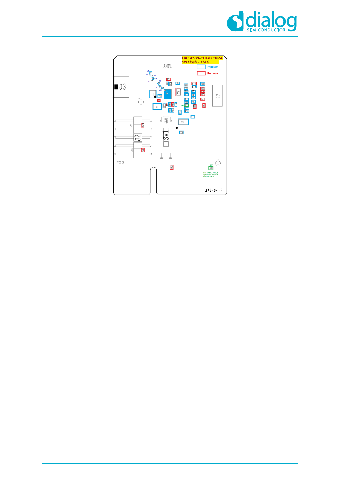
UM-B-114
DA14531 Development Kit Pro Hardware User Manual
User Manual
Revision 1.0
25-Oct-2019
CFR0012
74 of 80
© 2019 Dialog Semiconductor
Figure 72: Resistor and Jumper Settings for DA14531 FCGQFN24 PRO-DB
UM-B-114
DA14531 Development Kit Pro Hardware User Manual
User Manual
Revision 1.0
25-Oct-2019
CFR0012
75 of 80
© 2019 Dialog Semiconductor
Appendix F Enabling UART, JTAG and 32.768 kHz Crystal
F.1 UART (2-wire), JTAG, and 32.768 kHz Crystal
In this configuration, the 2-wire UART, JTAG, 32.768 kHz crystal, and reset are applied. No cables
are required because the signal assignment is done on the PRO-DB with proper resistor mounting. In
PRO-MB, the appropriate jumper setting is applied on J1.
Table 24: Pin Assignment for DA14531 WLCSP17 PRO-DB
Configuration
P0_0
P0_1
P0_2
P0_3
P0_4
P0_5
UART (2-wire), JTAG, and
32.768 kHz Crystal
UTX/Reset
URX
SWLCK
XTAL
XTAL
SWDIO
Table 25: Pin assignment for DA14531 FCGQFN24 PRO-DB
Configuration
P0_0
P0_1
P0_2
P0_3
P0_4
P0_10
UART (2-wire), JTAG, and
32.768 kHz Crystal
UTX/Reset
URX
SWLCK
XTAL
XTAL
SWDIO
Table 26: The Components for the Two Packages to Support 2-Wire UART, JTAG, and 32.768
kHz Crystal
Package
Populated components
Removed components
DA145xx PRO-MB
Apply jumpers:
J1:15-16, J1:17-18, J1:21-22, J1:23-
24, J1:25-26
J9:1-2, J9:3-4
J4: as per power configuration
J5: as per power configuration
DA14531- WLCSP17
R1, R2, R3, R4, R5,
R23, R24, R14, R15, R30,
Y2
R6, R19, R20, R21, R22, R25, R26
R27, R28, R29
R33, R34, R35
DA14531-FCGQFN24
R1, R2, R3, R6, R7, R8, R9, R10,
R12, R14, R16, R17, R18, R23,
R24, R30, R31, Y2
R4, R5, R11, R13, R15, R19, R20,
R21, R22, R25, R26, R27, R28, R29

UM-B-114
DA14531 Development Kit Pro Hardware User Manual
User Manual
Revision 1.0
25-Oct-2019
CFR0012
76 of 80
© 2019 Dialog Semiconductor
PRO-MB Jumpers (in Red)
WLCSP17
FCGQFN24
Figure 73: Resistor and Jumper Setting for PRO-MB (Top) and DA14531 PRO-DBs (Bottom) to
Support 2-Wire UART, JTAG, and 32.768 kHz Crystal
UM-B-114
DA14531 Development Kit Pro Hardware User Manual
User Manual
Revision 1.0
25-Oct-2019
CFR0012
77 of 80
© 2019 Dialog Semiconductor
F.2 Full UART and JTAG
In this configuration, the 4-wire full UART, JTAG, and reset are applied. No cables are required
because the signal assignment is done on the PRO-DB with proper resistor mounting. In PRO-MB,
the appropriate jumper setting is applied on J1.
Table 27: Pin Assignment for DA14531 WLCSP17 PRO-DB
Configuration
P0_0
P0_1
P0_2
P0_3
P0_4
P0_5
Full UART (4-wire) and JTAG
UTX/Reset
URX
SWLCK
UCTS
URTS
SWDIO
Table 28: Pin Assignment for DA14531 FCGQFN24 PRO-DB
Configuration
P0_0
P0_1
P0_2
P0_3
P0_4
P0_10
Full UART (4-wire) and JTAG
UTX/Reset
URX
SWLCK
UCTS
URTS
SWDIO
Table 29: The Components for the Two Packages to Support Full UART and JTAG
Package
Populated components
Removed components
PRO-MB
Apply jumpers
J1:11-12, J1:13-14, J1:15-16,
J1:17-18, J1:21-22, J1:23-24,
J1:25-26
J9:1-2, J9:3-4
J4: as per power configuration
J5: as per power configuration
DA14531 WLCSP17 PRO-DB
R1, R2, R3, R4, R5,
R14, R15, R23, R24, R25, R26,
R30
R6, R19, R20, R21, R22, R27,
R28, R29, R33, R34, R35, Y2
DA14531 FCGQFN24 PRO-DB
R1, R2, R3, R4, R5, R6, R7, R8,
R8, R9, R10, R12, R14, R16, R17,
R18, R23, R24, R25, R26, R30,
R31
R11, R13, R15, R19, R20, R21,
R22, R27, R28, R29, R33, R34,
R35, Y2
UM-B-114
DA14531 Development Kit Pro Hardware User Manual
User Manual
Revision 1.0
25-Oct-2019
CFR0012
78 of 80
© 2019 Dialog Semiconductor
PRO MB jumpers (in red)
WLCSP17
FCGQFN24
Figure 74: Resistor and Jumper Setting for PRO-MB (Top) and DA14531 PRO-DBs (Bottom) to
Support Full UART AND JTAG
UM-B-114
DA14531 Development Kit Pro Hardware User Manual
User Manual
Revision 1.0
25-Oct-2019
CFR0012
79 of 80
© 2019 Dialog Semiconductor
Revision History
Revision
Date
Description
1.1
24-Oct-2019
Editorial review.
1.0
15-Oct-2019
Initial version.
UM-B-114
DA14531 Development Kit Pro Hardware User Manual
User Manual
Revision 1.0
25-Oct-2019
CFR0012
80 of 80
© 2019 Dialog Semiconductor
Status Definitions
Status
Definition
DRAFT
The content of this document is under review and subject to formal approval, which may result in modifications or
additions.
APPROVED
or unmarked
The content of this document has been approved for publication.
Disclaimer
Unless otherwise agreed in writing, the Dialog Semiconductor products (and any associated software) referred to in this document are not
designed, authorized or warranted to be suitable for use in life support, life-critical or safety-critical systems or equipment, nor in applications
where failure or malfunction of a Dialog Semiconductor product (or associated software) can reasonably be expected to result in personal injury,
death or severe property or environmental damage. Dialog Semiconductor and its suppliers accept no liability for inclusion and/or use of Dialog
Semiconductor products (and any associated software) in such equipment or applications and therefore such inclusion and/or use is at the
customer’s own risk.
Information in this document is believed to be accurate and reliable. However, Dialog Semiconductor does not give any representations or
warranties, express or implied, as to the accuracy or completeness of such information. Dialog Semiconductor furthermore takes no
responsibility whatsoever for the content in this document if provided by any information source outside of Dialog Semiconductor.
Dialog Semiconductor reserves the right to change without notice the information published in this document, including, without limitation, the
specification and the design of the related semiconductor products, software and applications. Notwithstanding the foregoing, for any automotive
grade version of the device, Dialog Semiconductor reserves the right to change the information published in this document, including, without
limitation, the specification and the design of the related semiconductor products, software and applications, in accordance with its standard
automotive change notification process.
Applications, software, and semiconductor products described in this document are for illustrative purposes only. Dialog Semiconductor makes
no representation or warranty that such applications, software and semiconductor products will be suitable for the specified use without further
testing or modification. Unless otherwise agreed in writing, such testing or modification is the sole responsibility of the customer and Dialog
Semiconductor excludes all liability in this respect.
Nothing in this document may be construed as a license for customer to use the Dialog Semiconductor products, software and applications
referred to in this document. Such license must be separately sought by customer with Dialog Semiconductor.
All use of Dialog Semiconductor products, software and applications referred to in this document is subject to Dialog Semiconductor’s Standard
Terms and Conditions of Sale, available on the company website (www.dialog-semiconductor.com) unless otherwise stated.
Dialog, Dialog Semiconductor and the Dialog logo are trademarks of Dialog Semiconductor Plc or its subsidiaries. All other product or service
names and marks are the property of their respective owners.
© 2019 Dialog Semiconductor. All rights reserved.
RoHS Compliance
Dialog Semiconductor’s suppliers certify that its products are in compliance with the requirements of Directive 2011/65/EU of the European
Parliament on the restriction of the use of certain hazardous substances in electrical and electronic equipment. RoHS certificates from our
suppliers are available on request.
Contacting Dialog Semiconductor
United Kingdom (Headquarters)
Dialog Semiconductor (UK) LTD
Phone: +44 1793 757700
Germany
Dialog Semiconductor GmbH
Phone: +49 7021 805-0
The Netherlands
Dialog Semiconductor B.V.
Phone: +31 73 640 8822
North America
Dialog Semiconductor Inc.
Phone: +1 408 845 8500
Japan
Dialog Semiconductor K. K.
Phone: +81 3 5769 5100
Taiwan
Dialog Semiconductor Taiwan
Phone: +886 281 786 222
Hong Kong
Dialog Semiconductor Hong Kong
Phone: +852 2607 4271
Korea
Dialog Semiconductor Korea
Phone: +82 2 3469 8200
China (Shenzhen)
Dialog Semiconductor China
Phone: +86 755 2981 3669
China (Shanghai)
Dialog Semiconductor China
Phone: +86 21 5424 9058
Email:
enquiry@diasemi.com
Web site:
www.dialog-semiconductor.com
 Loading...