

Page 1

GreenPAK Designer
User Guide
Dialog Semiconductor
Corporate Headquarters
2560 Mission College Blvd
Santa Clara, CA 95054
USA
Phone: +1 408 845 8500
http://www.dialogsemiconductor.com
Dialog Semiconductor www.dialog-semiconductor.com
12/24/2020 1
GreenPAK Designer 6.25
GreenPAK
Page 2

Copyrights
Copyright © 2010-2020 Dialog Semiconductor. The information contained herein is subject to change without
notice. Dialog Semiconductor assumes no responsibility for the use of any circuitry other than circuitry embodied
in a Dialog product. Nor does it convey or imply any license under patent or other rights. Dialog products are not
warranted nor intended to be used for medical, life support, life saving, critical control or safety applications,
unless pursuant to an express written agreement with Dialog. Furthermore, Dialog does not authorize its products
for use as critical components in life-support systems where a malfunction or failure may reasonably be expected
to result in significant injury to the user. The inclusion of Dialog products in life-support systems application
implies that the manufacturer assumes all risk of such use and in doing so indemnifies Dialog against all charges.
GreenPAK Designer™, GreenPAK Programmer™ and GreenPAK™ are trademarks of Dialog Semiconductor. All
other trademarks or registered trademarks referenced herein are property of the respective corporations.
Any Source Code (software and/or firmware) is owned by Dialog Semiconductor (Dialog) and is protected by and
subject to worldwide patent protection (United States and foreign), United States copyright laws and international
treaty provisions. Dialog hereby grants to licensee a personal, non-exclusive, non-transferable license to copy,
use, modify, create derivative works of, and compile the Dialog Source Code and derivative works for the sole
purpose of creating custom software and or firmware in support of licensee product to be used only in conjunction
with a Dialog integrated circuit as specified in the applicable agreement. Any reproduction, modification,
translation, compilation, or representation of this Source Code except as specified above is prohibited without the
express written permission of Dialog.
Disclaimer: DIALOG MAKES NO WARRANTY OF ANY KIND, EXPRESS OR IMPLIED, WITH REGARD TO
THIS MATERIAL, INCLUDING, BUT NOT LIMITED TO, THE IMPLIED WARRANTIES OF MERCHANTABILITY
AND FITNESS FOR A PARTICULAR PURPOSE. Dialog reserves the right to make changes without further
notice to the materials described herein. Dialog does not assume any liability arising out of the application or use
of any product or circuit described herein. Dialog does not authorize its products for use as critical components in
life-support systems where a malfunction or failure may reasonably be expected to result in significant injury to
the user. The inclusion of Dialog product in a life-support systems application implies that the manufacturer
assumes all risk of such use and in doing so indemnifies Dialog against all charges. Use may be limited by and
subject to the applicable Dialog software license agreement.
Dialog Semiconductor www.dialog-semiconductor.com
12/24/2020 2
GreenPAK
GreenPAK Designer 6.25
Page 3

Contents
1. Introduction
1.1 Application Overview ............................................................................................................................ 5
1.2 System Requirements ......................................................................................................................... 5
1.3 Support ................................................................................................................................................ 6
1.4 Acronyms.............................................................................................................................................. 6
2. GreenPAK Designer Launcher................................................................................................................... 7
3. GreenPAK Designer
3.1 GreenPAK Designer Overview............................................................................................................. 8
3.1.1 Main Menu...................................................................................................................................... 10
3.1.2 Tool Bars........................................................................................................................................ 11
3.1.3 Work Area....................................................................................................................................... 13
3.1.4 Properties Panel............................................................................................................................. 14
3.1.5 Components List............................................................................................................................. 14
3.1.6 Color Scheme................................................................................................................................. 14
3.2 Creating a Project................................................................................................................................. 15
3.2.1 Updating Existing Projects.............................................................................................................. 15
3.2.2 Lock NVM Window......................................................................................................................... 15
3.2.3 Project Settings Window................................................................................................................. 16
3.3 Configuring Chip Components............................................................................................................. 17
3.3.1 Placing Components....................................................................................................................... 17
3.3.2 Setting Chip Components Parameters........................................................................................... 17
3.4 Specifying Interconnections.................................................................................................................. 18
3.4.1 Wire Types..................................................................................................................................... 20
3.4.2 Set/Erase Label.............................................................................................................................. 22
3.5 Specifying the Pinout ........................................................................................................................... 23
3.5.1 Port Connections............................................................................................................................ 23
3.5.2 Port Drive Modes............................................................................................................................ 23
3.6 Navigation............................................................................................................................................. 24
3.7 Keyboard commands............................................................................................................................ 24
3.8 GreenPAK Designer Settings............................................................................................................... 26
3.9 Legend Box.......................................................................................................................................... 28
3.10 Updating GreenPAK Designer............................................................................................................ 29
3.11 Help Window...................................................................................................................................... 30
3.12 Demo board and Demo mode............................................................................................................ 31
3.13 Snipping Tool...................................................................................................................................... 32
3.14 EPG Waveforms Editor....................................................................................................................... 33
4. Print Function
4.1. Print Editor........................................................................................................................................... 36
4.2. Print Editor Preview Window................................................................................................................ 43
4.3. Print..................................................................................................................................................... 45
5. Rules Checker........................................................................................................................................... 46
6. GreenPAK Debug Tool
6.1. Types of Areas..................................................................................................................................... 50
Dialog Semiconductor www.dialog-semiconductor.com
12/24/2020 3
GreenPAK
GreenPAK Designer 6.25
Page 4

6.2. Generators........................................................................................................................................... 54
6.2.1. General Option in Signal Wizard Modes........................................................................................ 55
6.2.2. Period Modes................................................................................................................................. 57
6.2.3. Logic Generator............................................................................................................................. 59
6.2.4. I2C Generator................................................................................................................................ 60
6.2.5. Signal (Analog) Generator............................................................................................................. 62
6.2.6. Custom Signal Wizard................................................................................................................... 69
6.2.7. VDD/VDD2 Power Signal Generator............................................................................................. 72
6.3. Expansion Connector........................................................................................................................... 73
6.4. Control Panel.......................................................................................................................................... 73
7. Asynchronous State Machine
7.1. ASM block............................................................................................................................................ 84
7.2. ASM Editor........................................................................................................................................... 85
8. GreenPAK Simulation................................................................................................................................ 87
9. Designing Overview
9.1. SLG46721 Properties Interpretation.................................................................................................... 97
A. Example Projects...................................................................................................................................... 131
B. Major features history ............................................................................................................................... 132
Dialog Semiconductor www.dialog-semiconductor.com
12/24/2020 4
GreenPAK
GreenPAK Designer 6.25
Page 5

1. Introduction
This document describes the installation and usage of Dialog GreenPAK® Designer software. This software can
be used as a stand-alone application for the firmware development and for GreenPAK chips programming. If the
information in this guide is not sufficient to resolve issues experienced with GreenPAK Designer, refer to the
resources listed under the Support section.
Features that are common for GreenPAK 3 Designer, GreenPAK 4 Designer, GreenPAK 5 Designer and
GreenPAK 6 Designer are described in chapters with a GreenPAK Designer general name. The differences are
described in separate chapters.
1.1 Application Overview
Each GreenPAK Designer (GreenPAK 3 Designer, GreenPAK 4 Designer, GreenPAK 5 Designer, GreenPAK 6
Designer) is a full-featured integrated development environment (IDE) that allows you to specify exactly how you
want the device to be configured. This provides you direct access to all GreenPAK device features and complete
control over the routing and configuration options. GreenPAK Designer will be used as a general name for
GreenPAK 3-6 Designer.
GreenPAK Designer has an integrated programming tool that allows you to program configured design into your
GreenPAK chip. With this tool you can also read an already programmed chip and export its data to the Designer.
Designer will generate a project, which has the same configuration as chip.
To start working with GreenPAK Designer please take the following steps:
Download and install GreenPAK Designer software;
Select what components you need;
Interconnect and configure components;
Specify the pinout;
Test your design with the Emulation Tool;
Use appropriate GreenPAK development platform to program your project into GreenPAK chip. You can
find your kit on Dialog's webstore.
1.2 System requirements
PC System Configuration
Minimum System Requirements for Dialog GreenPAK Designer:
CPU: 1800MHz
System Memory (RAM): 512MB
Graphics Card: 128MB
Free Hard Disk Space: 200MB
Operating System: Windows 7/8.1/10, MAC OS X (v10.8 or higher), Ubuntu 18.04 (32, 64-bit), Debian 10 (32, 64bit).
Dialog Semiconductor www.dialog-semiconductor.com
12/24/2020 5
GreenPAK
GreenPAK Designer 6.25
Page 6

1.3 Support
Free support for GreenPAK is available online at http://www.dialog-semiconductor.com
Also click Help- > Social in GreenPAK Designer and get access to Facebook, Twitter, LinkedIn and Dialog TV.
For software updates, please go to the Software page on our website.
You can find all these resources in the Help menu of GreenPAK Designer.
1.4 Acronyms
These are the acronyms used in the User Guide.
Table 1-1. Acronyms
Acronym Description
GPD GreenPAK Designer
GPP GreenPAK Programmer
IDE Integrated Development Environment
I/O Input/Output
IC Integrated Circuit
OE Output Enable
USB Universal Serial Bus
GPIO General Purpose Input / Output
GPI General Purpose Input
GPO General Purpose Output
NMOS N-channel MOSFET
(metal-oxide-semiconductor field-effect transistor)
PMOS P-channel MOSFET
(metal-oxide-semiconductor field-effect transistor)
ASM Asynchronous State Machine
Dialog Semiconductor www.dialog-semiconductor.com
12/24/2020 6
GreenPAK
GreenPAK Designer 6.25
Page 7

2. GreenPAK Designer Launcher
This section describes GreenPAK Designer launcher application and its features.
Figure 2-1. GreenPAK Designer Launcher User Interface
GreenPAK Designer launcher:
• Welcome – welcome page with short information and tips for new users.
• Develop – on this page user can select chip revision to start new project for required revision:
SLG46721V, SLG46722V, SLG46108V, SLG46110V, SLG46116V, SLG46117V, SLG46120V/P,
SLG46121V, SLG46125M, SLG46127M, SLG46169V, SLG46170V, SLG46621V, SLG46620V/G/-AG,
SLG46625-AP, SLG46140V, SLG46531V, SLG46532V, SLG46533V/M, SLG46534V, SLG46535V,
SLG46536V, SLG46537V/M, SLG46538V/M, SLG46538-AP, SLG46517M, SLG46580V, SLG46582V,
SLG46583V, SLG46585M, SLG46880V, SLG46880-AP, SLG46881V, SLG46824V/G, SLG46826V/G,
SLG46827-AG, SLG46828V, SLG46855V/-AP, SLG46857-AP, SLG46811V, SLG46867M, SLG47105V,
SLG47004V.
• Demo – on this page user can start GreenPAK Designer in Demo mode for selected Demo project and
read information about it.
• Recovery Files – page with restored files after crash or freeze. Files was saved with Autosave feature in
predetermined time intervals.
New – starts new project for selected chip revision (or double-click with left mouse button on selected chip
revision icon);
Open – opens existing project, automatically selects chip revision;
Close – close GreenPAK Designer Launcher.
Dialog Semiconductor www.dialog-semiconductor.com
12/24/2020 7
GreenPAK Designer 6.25
GreenPAK
Page 8

3. GreenPAK Designer
This section describes GreenPAK Designer application and its features.
3.1 GreenPAK Designer Interface Overview
GreenPAK Designer consists of: main menu, toolbar, main work area, output window, properties panel and
components list (see Figure 3-1, Figure 3-2).
Figure 3-1. GreenPAK User Interface
Dialog Semiconductor www.dialog-semiconductor.com
12/24/2020 8
GreenPAK
GreenPAK Designer 6.25
Page 9

Figure 3-2. GreenPAK 4 User Interface
Dialog Semiconductor www.dialog-semiconductor.com
12/24/2020 9
GreenPAK
GreenPAK Designer 6.25
Page 10

3.1.1. Main Menu
Main menu contains controls described below:
- File
New – start new or open existing project from GPAK Launcher;
Open – open existing project in GP Designer;
Clear – clear project and select revision for specified chip;
Open in current – open existing project for specified chip;
Save – save current project;
Save as – save current project in specified location;
Import NVM bits – load configuration bits from text file;
Export NVM bits – save configuration bits to text file;
Print – start Print Editor referring item 4;
Print Sch (Beta) – simple print feature without detailed block information;
Project Information;
Application Notes – opens examples web page;
Exit program – close GPD;
- Edit
Rotate Left – rotate a selected block counterclockwise;
Rotate Right – rotate a selected block clockwise;
Flip Horizontal – horizontal reflection of a selected block
Flip Vertical – vertical reflection of a selected block
Align Horizontal – horizontal alignment of selected blocks
Align Vertical – vertical alignment of selected blocks
Set Label – creating a text label for selected blocks
Erase Label – erasing text labels near selected blocks
Set Wire – enable wire creating mode;
Erase Wire – enable wire erase mode;
- View
Zoom in – increase the work area scale;
Zoom out – decrease the work area scale;
Fit work area – tune scale to show all blocks visible in project;
Zoom 1:1 – set default scale;
Full-screen mode – switch to full-screen mode
Pan mode – enable/disable scene move in pan mode;
Show hints – enable/disable hints for blocks on the scene;
Properties – show/hide Properties panel;
Component Library – list of external components for Software Simulation;
Components – show/hide Green PAK blocks list;
NVM Viewer – show/hide NVM bits viewer;
Rules Checker Output;
Dialog Semiconductor www.dialog-semiconductor.com
12/24/2020 10
GreenPAK
GreenPAK Designer 6.25
Page 11

- Tools
Debug – this tool is included for convenient project testing;
Rules Checker – checks current design for correct settings;
Comparison – compares bits of two projects;
ASM Editor – allows to configure the State Machine using state diagram and set the output
configuration for SM Output block;
I2C Tools – enhanced I2C tools with I2C snapshot Reconfigurator (only in GreenPAK 5-6
Designer);
- Options
Settings – default projects folder, autosave, toolbars position, recovery, shortcuts and update
options;
- Help
Help – show help window;
User Guides – open User guides web page;
Legend box – show the color legend box;
Dialog web site – open Dialog official web site;
Software and documentation – open Software & Dock web page;
Dialog web store – open Dialog chip store;
Design support – web page with training courses and videos;
Contact Us – web form with request;
Social – Dialog Semiconductor in social networks;
Application Notes – open examples web page;
Datasheet – open documentation web page;
Updater – open GreenPAK update tool;
About GreenPAK Designer – show information about GPD versions modification.
3.1.2. Tool-bars
Toolbar provides a quick access to frequently used functions. There are 8 tool-bars:
- File
New;
Open;
Save;
Print;
- Undo
Undo;
Redo;
- Wire
Set wire;
Erase Wire;
- Label
Set Label;
Erase Label;
Dialog Semiconductor www.dialog-semiconductor.com
12/24/2020 11
GreenPAK
GreenPAK Designer 6.25
Page 12

- Item editor
Rotate Left;
Rotate Right;
Flip Horizontal;
Flip Vertical;
Align Horizontal;
Align Vertical;
- Tools
Rules Checker;
Debug;
ASM Editor (only in GreenPAK 5-6 Designer);
Project Settings;
Project Info;
- Panel switcher
Properties;
Components;
NVM Viewer;
- Navigation
Zoom slider – adjust scale;
Zoom 1:1;
Fit work area;
Full screen mode;
Pan mode;
Show item hint;
Dialog Semiconductor www.dialog-semiconductor.com
12/24/2020 12
GreenPAK
GreenPAK Designer 6.25
Page 13

3.1.3. Work Area
Work area contains all blocks available in GreenPAK chip and their connections. In GreenPAK 4 Designer
(SLG46620V and SLG46621V) work area consist of 2 matrices: Matrix0 and Matrix1(Figure 3-4). The components
of each matrix can be interconnected through 10 input and 10 output ports.
Matrices window placement define buttons:
- Matrix 0 (full screen);
- Matrix 1 (full screen);
- Vertical placement (2 matrices);
- Horizontal placement (2 matrices);
- One of matrices in separate window or monitor.
Figure 3-4. Two matrices of GreenPAK 4 Designer.
Three types of components connection:
- Connectivity matrix connections (green) – user can connect any output to any input through wiring tool;
- Settings defined connections (orange) – these connections are predefined and depend on block settings;
- Buses (wide orange line) – buses also depend on block settings. All buses are 8-bit wide.
All blocks can be moved using mouse or keyboard (Ctrl+Arrow Keys or Alt+Arrow Keys) and rotated. You can
move a few blocks at the same time by using multiple select option. Rotation, flipping and alignment is also
available for more than one block at a time.
Dialog Semiconductor www.dialog-semiconductor.com
12/24/2020 13
GreenPAK
GreenPAK Designer 6.25
Page 14

3.1.4. Properties Panel
Properties panel contains all settings available for selected chip component. The panel is divided in two partitions:
Properties and Connections. Properties division contains settings and parameters that could be specified for a
selected block. Connection division contains settings which control the predefined connections to the selected
block. Last division could not be present in some blocks. Some parameters and settings are common for a few
blocks. There are 2 types of controlling elements Edit Box and Drop List. To change settings in Drop List you
can click and select action or place the mouse pointer over selected list and scroll by mouse wheel. To enter
value into the Edit Box you can use keyboard, mouse scroll or buttons at the right. After finishing all configurations
press Apply button to confirm changes. If you want to discard changes you can press Reset button with
options: reset settings to default or reset connections to default.
3.1.5. Components List
The Components list is an instrument that contains all blocks available in chip. It provides user with the possibility
to show/hide unused blocks. You cannot hide blocks that are connected by any type of lines. In the GreenPAK
chip there are connections which are beyond the connectivity matrix. They are controlled by settings of proper
components and cannot be fully disconnected. That's why there are some blocks that cannot be hidden. Hidden
blocks retain their configuration. For this reason, be sure to configure hidden components properly. You can show/
hide selected blocks by using the check/un-check feature on the list. In order to show a group of blocks, doubleclick on the check box of the desired group. In order to hide a group use a single click.
There are two buttons at the bottom of the components list – Show all (shows all blocks) and Hide all (hides all
blocks which are not connected to a circuit). Also user can use filter to find required components.
User can drag&drop any component from Component List to the workarea to the right place:
3.1.6 Color Scheme
Components:
Mode Description
Normal Selected
Turned on
Turned off
I/O PAD
Components Pin Tips:
Color Value
User can connect wire to this pin
Pin has already been connected (and there cannot be any other connections to this pin)
User can connect wire to this pin only after changing component option
Inner connection, user cannot connect wire to this pin
External I/O Pin (I/O from chip)
Dialog Semiconductor www.dialog-semiconductor.com
12/24/2020 14
GreenPAK
GreenPAK Designer 6.25
Page 15

3.2 Creating a Project
To create a new GreenPAK Designer project start GPD Launcher or go to File->New or click the “New” icon
on the toolbar. While creating new project in GreenPAK Designer please choose chip revision for current project
and specify operating conditions – VDD and Temperature.
Figure 3-4. Set Chip Revision and Operating conditions.
A new project will be created in current window and all unsaved changes will be lost. Also you can start a new
GreenPAK Designer copy and it will be loaded with the blank project. By default the project is configured for
minimal power consumption and some components are disabled. All disabled components are darker and colored
in red after selection. GreenPAK 3-6 projects use [.aap,.hvpak,.gp3,.gp4,.gp5,.gp6] file extension. It contains
information about position, rotation/flipping and configuration of chip blocks, all wire connections, and bit file
sequence settings of test mode, etc. Interface settings will not be saved in the Project file.
3.2.1 Updating Existing Projects
If you load an existing project created by a previous version of GreenPAK Designer and want to save changes, it
will be saved in the updated file format.
3.2.2 Lock NVM Window
Figure 3-5. NVM Options.
Lock status – blocks NVM reading. A programmed project becomes unavailable for chip reading. Though chip is
still applicable for the emulation.
Pattern ID – gives an ID (1-255) to the project. The ID will be put in the chip after programming, and also will be
read back during “chip reading” operation.
Dialog Semiconductor www.dialog-semiconductor.com
12/24/2020 15
GreenPAK
GreenPAK Designer 6.25
Page 16

3.2.3 Project Settings Window
Figure 3-6. Project Settings General tab
GPIO quick charge – this option will temporarily enable 2k resistor for ~1μs duration in parallel to internal
pull-up/downs during power on, before reset signal is released to internal blocks. For example, this option should
be used to ensure the internal pull-up rise-time is fast enough to be detected as high level during power-on.
Otherwise, a rising edge with weak internal pull-up can be quite slow, and miss detection as a high-level because
of too slow of risetime.
Figure 3-7. Project Settings Security tab
Lock status – blocks NVM reading/writing. A programmed project becomes unavailable for chip reading or for chip
writing via I2C Tools for chips with I2C Serial Communication (see chip datasheet). The chip is still applicable for
emulation.
Pattern ID – gives an ID (1-254/65534) to the project. The ID will be put in the chip after programming, and also
will be read while “chip reading” operates.
Dialog Semiconductor www.dialog-semiconductor.com
12/24/2020 16
GreenPAK
GreenPAK Designer 6.25
Page 17

3.3 Configuring Chip Components
3.3.1 Placing Components
When you open GreenPAK Designer it will start with a blank project. A blank project contains pins and blocks
which cannot be hidden. Components can be moved, rotated, flipped and aligned. In order to move a component,
simply drag it where you want by clicking the left mouse button. To rotate/flip/align component select it and press
the “Rotate/Flip/Align” buttons on the toolbar or select
Rotate/Flip/Align in the main menu.
3.3.2 Setting Chip Components Parameters
Each chip component has different parameters. Some components have parameters that are shared with other
components. Changes in one block cause changes in other blocks. Component settings are available at
component Properties panel (Figure 3-8) which appears after double-clicking on the component. Properties
panel consists of three parts: Properties, Connections, and Information. Properties section contains all settings of
a selected component. Connections section allows you to configure connections that couldn’t be made using
wiring tool. Information section contains short information about parameters of selected component. After making
changes in Properties panel click the “Apply” button to save changes. If you do not click the “Apply” button and
select another block, a save changes message box will appear.
Figure 3-8. Properties Panel
Reset connections and/or settings to default: this option allows to reset NVM bits, components properties, wire
connections from/to component.
Dialog Semiconductor www.dialog-semiconductor.com
12/24/2020 17
GreenPAK
GreenPAK Designer 6.25
Page 18

3.4 Specifying Interconnections
You can interconnect chip components to achieve the necessary functionality. To make a connection please select
Set wire on the Wire toolbar or from the main menu. Next, click the first and second pins that you want
to connect. After selecting the first pin, GPD highlights allowed connections in green. If you click the first pin and
then decide to exit line creating mode press Esc or the right mouse button.
Figure 3-9.
Also you can manually correct the created wires.
You can move horizontal lines up and down, vertical lines left and right (Figure 3-10).
Figure 3-10.
You can move points on the wire (Figure 3-11).
Figure 3-11.
In order to create additional points on the line use the double click (Figure 3-12).
Figure 3-12.
Dialog Semiconductor www.dialog-semiconductor.com
12/24/2020 18
GreenPAK
GreenPAK Designer 6.25
Page 19

Only the green color pins can be connected Using Wire Creating tool. Some components have pins that are not
allowed to be connected using wiring tool. Connections between such pins (orange dotted line and violet pin
color) and buses can be made only by changing settings in Connections section of the Properties panel of
proper components. In this case violet pins can change color to green and user can connect them using wiring
tool. Orange wires will be automatically generated. Orange wires also can be modified by user. Input pins without
connections are considered to be tied to ground.
In order to delete wire please select Erase wire at the Wire tool-bar and click on the selected wire.
Only green wires can be deleted.
Additional controls for add/remove wires:
Hold button to force wire mode:
• Shift: for Set Wire;
• Alt: for Erase Wire;
Action with multiple wires:
• Hold Ctrl+Shift and click on pin: add multiple wires from the same source pin;
• Hold Ctrl+Alt and click on wire: remove all wires from source pin;
• Hold Ctrl: works as Ctrl+Shift or Ctrl+Alt based on current wire mode;
Move network
Move network feature provides the fastest way to reconnect all matrix wires from any pin to another. Simply click
on wire with right mouse button and select Move network in Context menu
Figure 3-13. Move network in Context menu
Select new source from list in Move network window. User can select new source only from list of visible blocks or
from list of all blocks.
Dialog Semiconductor www.dialog-semiconductor.com
12/24/2020 19
GreenPAK
GreenPAK Designer 6.25
Page 20

Figure 3-14. Move network window
3.4.1 Wire Types
Figure 3-15. Green Line
Green lines in GreenPAK Designer software tools are used to mark manual wires. Using them you can manually
connect necessary blocks to operate in the desired way. You can connect block output to multiple inputs, but
wiring of different outputs to one input is impossible.
Figure 3-16. Orange Line
Orange lines are used to mark the internal functional bounds of the chip blocks. They do not have the impact on
chip operation until the proper function is used. These lines can’t be erased.
Dialog Semiconductor www.dialog-semiconductor.com
12/24/2020 20
GreenPAK
GreenPAK Designer 6.25
Page 21

Figure 3-17. Bold Orange Line
Bold orange lines (like the orange lines) mark the internal bounds. The difference is that the bold orange lines
mark 8-bit parallel data buses. These lines also cannot be erased. They do not have an impact on chip operation
until the proper function is used and the proper option is set.
Figure 3-18. Light Green Line
Light green lines are used to mark the shared connections. Their behavior is the same as the green lines.
Replacing wires by labels
This option converts wired connection to 2 labels (for output and input pins) and back (Figure 3-19). Name of the
label will be generated automatically: NETx, where x – random number. If output was connected to few inputs all
of them should have the same name. For changing the connection type use the context menu of the block, line or
label(NET).
Figure 3-19.Labeled connections
Available options for wire (context menu):
- Convert to labeled connection;
Available options for label (context menu):
- Convert to wired connection;
- Rename network;
- Remove connection.
Dialog Semiconductor www.dialog-semiconductor.com
12/24/2020 21
GreenPAK
GreenPAK Designer 6.25
Page 22

3.4.2 Set/Erase Label
Using Set/Erase Label the user can add/delete text label. The Set Label tool adds a text label to the selected
component or without connecting them to the specific component. The user can Attach label to component or
Detach label(s) from component(s). If no component is selected, then the user can select a component from the
list offered by the Set Label tool. The user can also choose text color. If the selected component already has a
label, Set Label tool can edit label text. If the user selects more than one component, it is possible to change the
text color without changing text in all components at once. If the user changes the text while more than one
component is selected, it will be changed on all selected components at once as well. Erase Label deletes text
label.
Figure 3-20. Add Label
Dialog Semiconductor www.dialog-semiconductor.com
12/24/2020 22
GreenPAK
GreenPAK Designer 6.25
Page 23

3.5 Specifying the Pinout
3.5.1 Port Connections
Pin blocks can be connected just like any other blocks using the Wiring Tool.
3.5.2 Port Drive Modes
GreenPAK chips have GPIO, GPO and GPI pin components. These components can be configured to work in the
following modes:
Digital in with Schmitt trigger;
Digital in without Schmitt trigger;
Low voltage digital in;
1x push pull;
2x push pull;
1x open drain NMOS;
2x open drain NMOS;
4x open drain NMOS;
1x open drain PMOS;
2x open drain PMOS;
1x 3-State Output;
2x 3-State Output;
Analog input;
Analog output;
Also, Pull-Up/Pull-Down resistors are configurable. To configure the pin component, open its parameters to set a
desired mode and pull-up/pull-down resistor. I/O pin components have input (IN), output (OUT) and output
enable (OE) pins. These pins are one-way directed, so you need to configure the pin component and connect the
proper pin. OUT pin is an output signal from the pin component. It corresponds to the signal from the input buffer.
IN pin is an input to the pin component. It accepts a signal from internal components. Output Enable (OE) signal
defines the Push-pull buffer state. Low OE signal switches buffer to Hi-Z state. High OE signal enables Push-pull
buffer regardless of selected component operating mode. It could be used for applications where bidirectional pins
are needed.
Dialog Semiconductor www.dialog-semiconductor.com
12/24/2020 23
GreenPAK
GreenPAK Designer 6.25
Page 24

3.6 Navigation
To navigate through project workspace use the View menu or toolbar. Use Zoom In , Zoom Out
buttons or slider to zoom workspace. If you want to see all project components click on Fit work area or
Zoom 1:1 . To navigate through work area you can use Pan mode . Pan mode also activates by
using middle mouse button.
To enable block's hint, press Show item hints button. A hint box pops up next to the item when the mouse
moves over the block.
3.7 Keyboard commands
To navigate through GreenPAK Designer use specific keyboard commands or shortcuts. List of commands
specified in the table:
Table 3-1. Keyboard commands
Keyboard command Action
Block moving on the scene
Alt+Arrow Keys Moves selected block on 1 pixel
Ctrl+Arrow Keys Moves selected block on 10 pixels
Connecting/Erasing wires
Hold Shift Forces Set wire while using Erase Wire
Hold Alt Forces Erase wire while using Set Wire
Hold Ctrl+mouse cursor Adds multiple wires from the same source
Hold Ctrl+Shift+mouse
cursor
Forces add of multiple wires from the same source while
using Erase Wire
Hold Ctrl+Alt+mouse
cursor
Forces remove of all wires from the network while using Set
Wire
Standard hotkeys
Ctrl+Z Undo
Ctrl+Y Redo
Ctrl+N New project
Ctrl+O Open project
Ctrl+S Save project
Ctrl+P Print Editor
Dialog Semiconductor www.dialog-semiconductor.com
12/24/2020 24
GreenPAK
GreenPAK Designer 6.25
Page 25

Ctrl+Q Exit program
Ctrl+L Rotate component Left
Ctrl+R Rotate component Right
Ctrl+H Flip component Horizontal
Ctrl+V Flip component Vertical
Ctrl+W Set Wire
Ctrl+E Erase Wire
Ctrl+F Filter on Components List
H Hide component
+ Zoom in
- Zoom out
F1 Help
F2 NVM Viewer
F3 Properties of component
F4 Components List
F5 Rules Checker
F9 Debug
F11 Fullscreen Mode
Debug hotkeys
Shift+E Emulation
Shift+I Info
Shift+L Log
Shift+N NVM Data
Shift+P Program
Shift+R Read
Shift+S Save Settings
Shift+T Test Mode
All other Designer main window actions can be configured by entering specific key sequence in Settings window
on Shortcuts tab. For ASM Editor user should enter key sequence in format: Ctrl+key.
Dialog Semiconductor www.dialog-semiconductor.com
12/24/2020 25
GreenPAK
GreenPAK Designer 6.25
Page 26

3.8 GreenPAK Designer Settings
GreenPAK Designer settings configure all basic options of program in several tabs (Figure 3-21). To open settings
select Options-> Settings in main menu.
Figure 3-21. Settings window
GreenPAK Designer settings window contains of tabs:
General:
• Default projects folder – defines path to users GPD project files;
• Projects recovery – activates autosave function, which allows to reduce the risk or impact of data loss in
case of a crash or freeze. Autosave function in predetermined time intervals will save your files and after
a critical problem will offer to restore these files in GreenPAK Designer Launcher on Projects files
recovery tab (Figure 3-22);
Dialog Semiconductor www.dialog-semiconductor.com
12/24/2020 26
GreenPAK
GreenPAK Designer 6.25
Page 27

Figure 3-22. Project files recovery tab in GPD Launcher
Designer:
• Pin hints – shows pin hints while block is selected or properties panel of component is visible:
• Look-Up Table (LUT) – allow usage of regular shape by default. For example, regular shape of NXOR:
Appearance:
• Window appearance – saves positions of toolbars/dock widgets and window geometry of GP Designer
work area;
• High DPI displays – enables GP Designer scalling on high DPI displays;
Shortcuts:
• On Shortcuts tab all GP Designer actions can be configured by entering specific key sequence. For ASM
Editor user should enter key sequence in format: Ctrl+key;
Updater:
• Scheduler – determines check for updates time: after Designer starts or Once per 1-7 days;
• Path – defines server for update and destination to download updates;
• Proxy – allow user to configure proxy for updates;
• Check configuration button – checks connection to server.
Default button:
• Resets settings to default parameters by categories or all at once.
Dialog Semiconductor www.dialog-semiconductor.com
12/24/2020 27
GreenPAK
GreenPAK Designer 6.25
Page 28

3.9 Legend Box
Legend box shows the color scheme of GreenPAK designer.
The user can open this window by clicking 'Legend box' button in 'Help' menu.
Figure 3-23. Legend Box View
Dialog Semiconductor www.dialog-semiconductor.com
12/24/2020 28
GreenPAK Designer 6.25
GreenPAK
Page 29

3.10. Updating GreenPAK Designer
There are two ways of updating the GreenPAK Designer:
• When updates are available – this information will be displayed. The user will get a chance to either
download a new version using the “OK”, or the “Cancel” to delay the update until the next program start.
After the download is finished, Designer automatically installs the software.
IMPORTANT: After finishing installation, restart the GreenPAK Designer software.
Figure 3-24. Updating GreenPAK Designer
• You can also find the latest GPD version at Software page of Dialog web site. For the best user
experience, keep your GreenPAK Designer up to date. Feel free to email suggested updates to the
developer to improve this program (Please refer to “About GreenPAK ” section of Help menu).
Configure Updater options on Updater tab in Designer Settings window (see Section 3.8 GreenPAK Designer
Settings)
Dialog Semiconductor www.dialog-semiconductor.com
12/24/2020 29
GreenPAK
GreenPAK Designer 6.25
Page 30

3.11 Help Window
To view information about a specific block, select the block and click 'Help' from the Help menu or press the 'F1'
button. A window will list the information about each block ('short info'). Press the 'detailed info' button for more
detailed information (Figure 3-25). If you don't select any block, you will be shown the information about all the
blocks. The 'Help' button on the property panel of each block provides the same information about the current
block.
Figure 3-25. Help Window
Dialog Semiconductor www.dialog-semiconductor.com
12/24/2020 30
GreenPAK
GreenPAK Designer 6.25
Page 31

3.12 Demo board and Demo mode
Demo board
Demo board is a special hardware with a mission to demonstrate some specific application of GreenPAK chip.
They have GreenPAK chip soldered on the board, already programmed with some specific project. They also
support I2C transferring that allows Designer to communicate with GreenPAK chip and change it NVM.
The exception is I2C Bridge which doesn’t have specific project and allows any project to be loaded in.
Demo board connection
After opening of Demo project, Designer waits for connecting of proper device:
Figure 3-26. Waiting for proper Demo board
Demo board detection
Figure 3-27. Demo board detected
After Proper Demo board detected (Figure 3-27), simple I2C tool activated:
• Write - sends current project’s NVM to device;
• I2C Virtual Inputs, I2C Virtual Outputs (with Add/Remove Probe tool) - opens I2C tools (see Section 6.4
Control Panel);
• I2C Reconfigurator – starts shapshots reconfigurator tool (see Section 6.4 Control Panel);
• Close - exits demo mode;
• Info button - shows all system and hardware information;
Designer’s Demo Mode
User can start designer in Demo mode, which means it will show specific project for selected demo and provide
tool to operate with demo board. Demo mode applies some restrictions on Designer functions as well as adds of a
new features. In general case it opens specific demo project, shows specific tool control panel and limits
operations with project file.
Exit demo mode
User can exit demo mode. This will decline all restrictions applied by demo mode, but keep current project open.
Dialog Semiconductor www.dialog-semiconductor.com
12/24/2020 31
GreenPAK
GreenPAK Designer 6.25
Page 32

3.13 Snipping Tool
Snipping Tool is screenshot tool for GreenPAK Designer workarea. It allows scene selection, copying or saving as
a file.
Click Tools → Snipping Tool, select style of screenshot area (Figure 3-28)
Figure 3-28. Snipping Tool window with style selection
Select area and copy to clipboard or save image in Bitmap/PNG/SVG format (Figure 3-29)
Figure 3-29. Snipping Tool window: export selection
Dialog Semiconductor www.dialog-semiconductor.com
12/24/2020 32
GreenPAK
GreenPAK Designer 6.25
Page 33

3.14 EPG Waveforms Editor
The Extended Pattern Generator (EPG) range is 92 bytes and at every rising edge of CLK input a byte from NVM
appears at the output. EPG shares its outputs with I2C Virtual Inputs. Configure Extended Pattern Generator in
EPG Waveforms Editor(Figure 3-30) using SPI, I2C, PWM or Manual type of generator.
Figure 3-30. EPG Waveforms Editor
Dialog Semiconductor www.dialog-semiconductor.com
12/24/2020 33
GreenPAK
GreenPAK Designer 6.25
Page 34
SPI generator has output pins, commands editor and samples resources meter (Figure 3-31).
Figure 3-31. SPI generator commands editor and resources meter
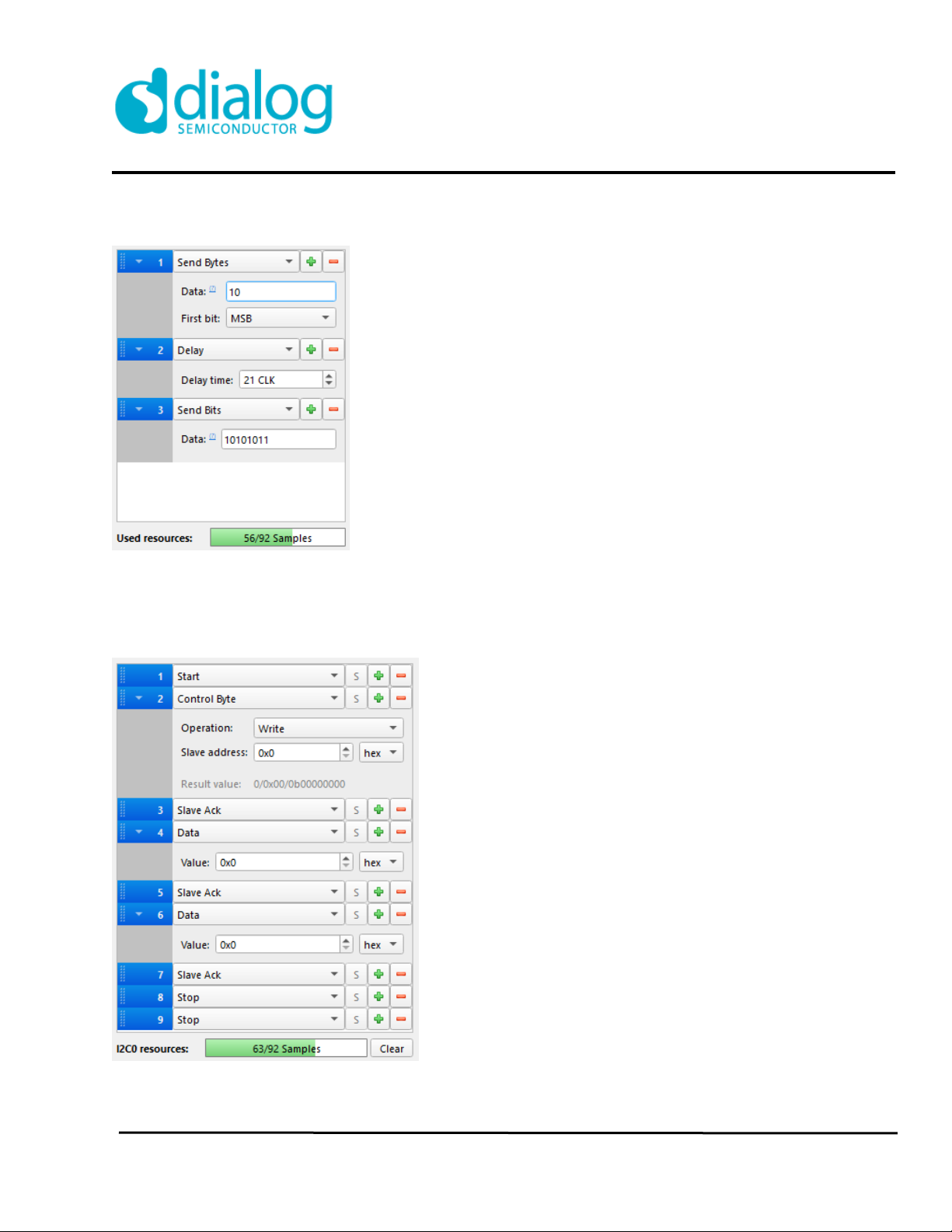
I2C generator has SDA and SCL output pins, commands editor and samples resources meter (Figure 3-32). In
editor user selects commands from list of Basic (start, stop, etc.) and GreenPAK access (Read/Write). “S” button
splits composite GP access commands in sequence of Basic commands.
Figure 3-32. I2C generator commands editor and resources meter
Dialog Semiconductor www.dialog-semiconductor.com
12/24/2020 34
GreenPAK
GreenPAK Designer 6.25
Page 35

PWM generator configures output pin, period duration, high level duration and phase shift (Figure 3-33).
Figure 3-33. PWM generator options
Manual generator configures output pin and bits values (Figure 3-34).
Figure 3-34. Manual generator options
Dialog Semiconductor www.dialog-semiconductor.com
12/24/2020 35
GreenPAK
GreenPAK Designer 6.25
Page 36
4. Print Function
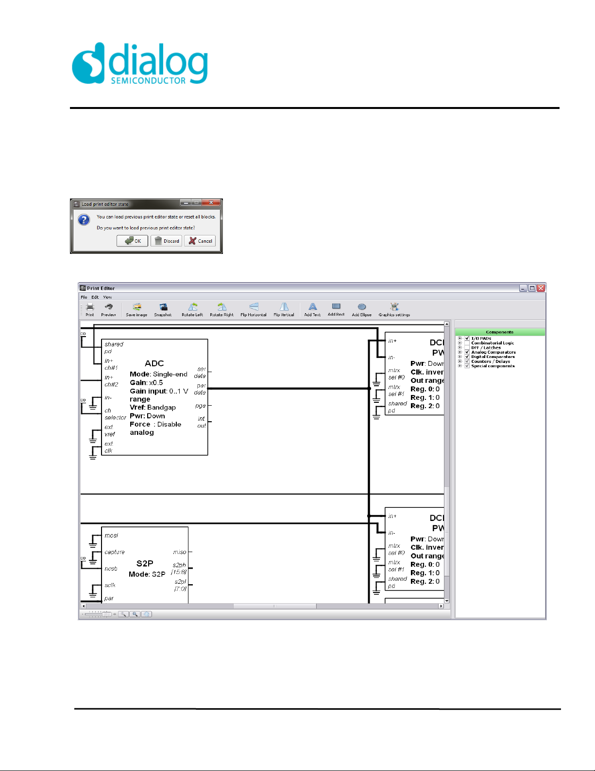
4.1. Print Editor
Print Editor feature consists of two main parts:
Editable working area, where the user can customize positions, view of components, and lines
connecting them.
Preview window where the user can set up the print preferences.
Editable working area shows all components which where used in the design.
Figure 4-1. Print Editor
Dialog Semiconductor www.dialog-semiconductor.com
12/24/2020 36
GreenPAK Designer 6.25
GreenPAK
Page 37
The Main Actions:
- User can hide or display any component using the Components list on the right.
- Each component in the work area is selectable and movable.
- Any component can be rotated or flipped.
Note: print editor settings will be saved before print editor's window is closed. It allows the user to repair previous
state during next opening.
Figure 4-2. Preview Window
Dialog Semiconductor www.dialog-semiconductor.com
12/24/2020 37
GreenPAK
GreenPAK Designer 6.25
Page 38
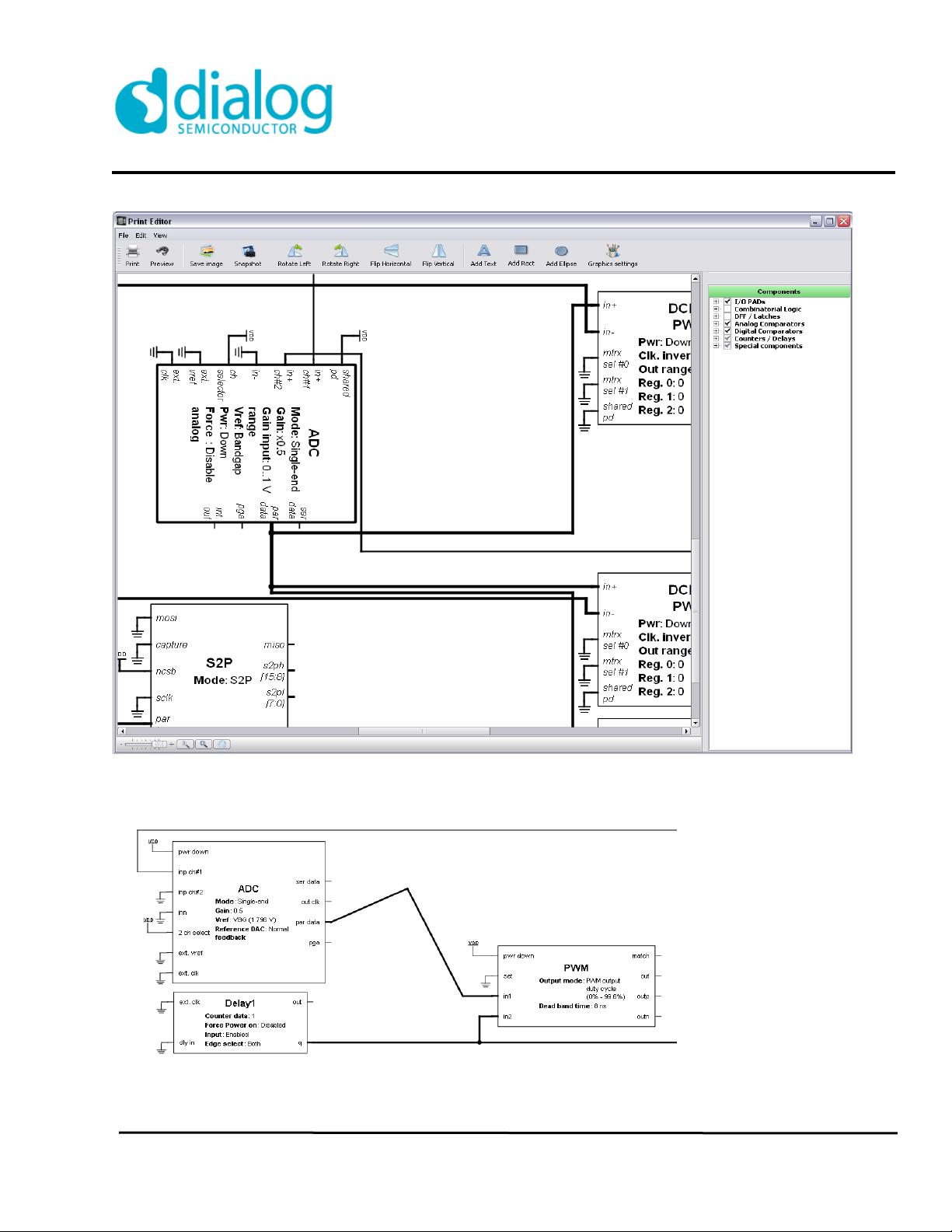
Figure 4-3. Preview Window
User can move lines and points to correct odd angled appearance.
Figure 4-4. Work sheet.
Working area
Dialog Semiconductor www.dialog-semiconductor.com
12/24/2020 38
GreenPAK
GreenPAK Designer 6.25
Page 39

Working area can be zoomed in or zoomed out.
User can add a text label to the schematics using the text tool.
Figure 4-5. Text Label
Figure 4-6. View with Text Label
Dialog Semiconductor www.dialog-semiconductor.com
12/24/2020 39
GreenPAK
GreenPAK Designer 6.25
Page 40

The user can add to the working area the custom figures including rectangle, rounded rectangle, ellipse etc.
Figure 4-7. Custom Figure
The user can also customize the main paint parameters.
Figure 4-8. Paint Parameters
You can see a small preview window which includes a painted rectangle with user-parameters.
Dialog Semiconductor www.dialog-semiconductor.com
12/24/2020 40
GreenPAK
GreenPAK Designer 6.25
Page 41

When the user adds a figure to the working area, one can customize the figure size by dragging black points on
the corners and sides. The user can view it only by moving the mouse pointer up to the figure.
Figure 4-9. Work Area
Dialog Semiconductor www.dialog-semiconductor.com
12/24/2020 41
GreenPAK
GreenPAK Designer 6.25
Page 42

The user can save a composed diagram into a graphics file or directly send it to the printer.
Figure 4-10. Save diagram
Dialog Semiconductor www.dialog-semiconductor.com
12/24/2020 42
GreenPAK Designer 6.25
GreenPAK
Page 43

4.2. Print Editor Preview Window
Preview window shows the composed and ready-to-print diagram. In this window, the user cannot change the
position of the components or the other elements in the diagram. The user can only choose the advanced settings
for printing or saving to the file.
Figure 4-11. Preview Window
Dialog Semiconductor www.dialog-semiconductor.com
12/24/2020 43
GreenPAK
GreenPAK Designer 6.25
Page 44
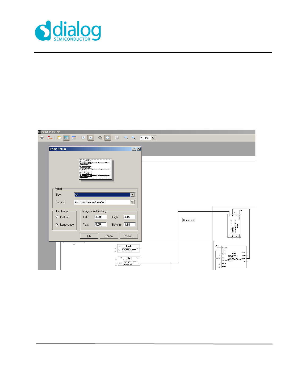
Main Actions
The user can:
• Choose orientation of the diagram on a paper (landscape or portrait)
• Fit the diagram to a page or keep the real size
• Fit to center
• Zoom in or zoom out
• Choose the size or type of paper
• Save the finished diagram into a PDF/Image file or print it out
Figure 4-12. Page Setup
Dialog Semiconductor www.dialog-semiconductor.com
12/24/2020 44
GreenPAK
GreenPAK Designer 6.25
Page 45
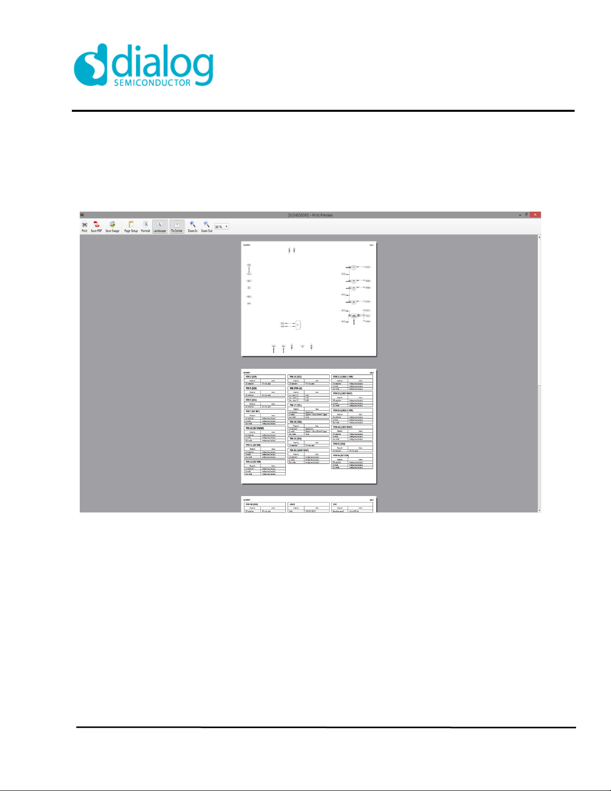
4.3. Print
Print window shows the composed and ready-to-print diagram with block properties and its values. In this window,
the user cannot change the position of the components or the other elements in the diagram. The user can only
choose the advanced settings for printing or saving to the file.
Figure 4-13. Print window with block properties and values
Print options:
• Choose orientation of the diagram on a paper (landscape or portrait)
• Fit diagram to center
• Zoom in or zoom out
• Choose the size or type of paper
• Save the finished diagram into a PDF/Image file
• Print diagram and block properties
Dialog Semiconductor www.dialog-semiconductor.com
12/24/2020 45
GreenPAK
GreenPAK Designer 6.25
Page 46
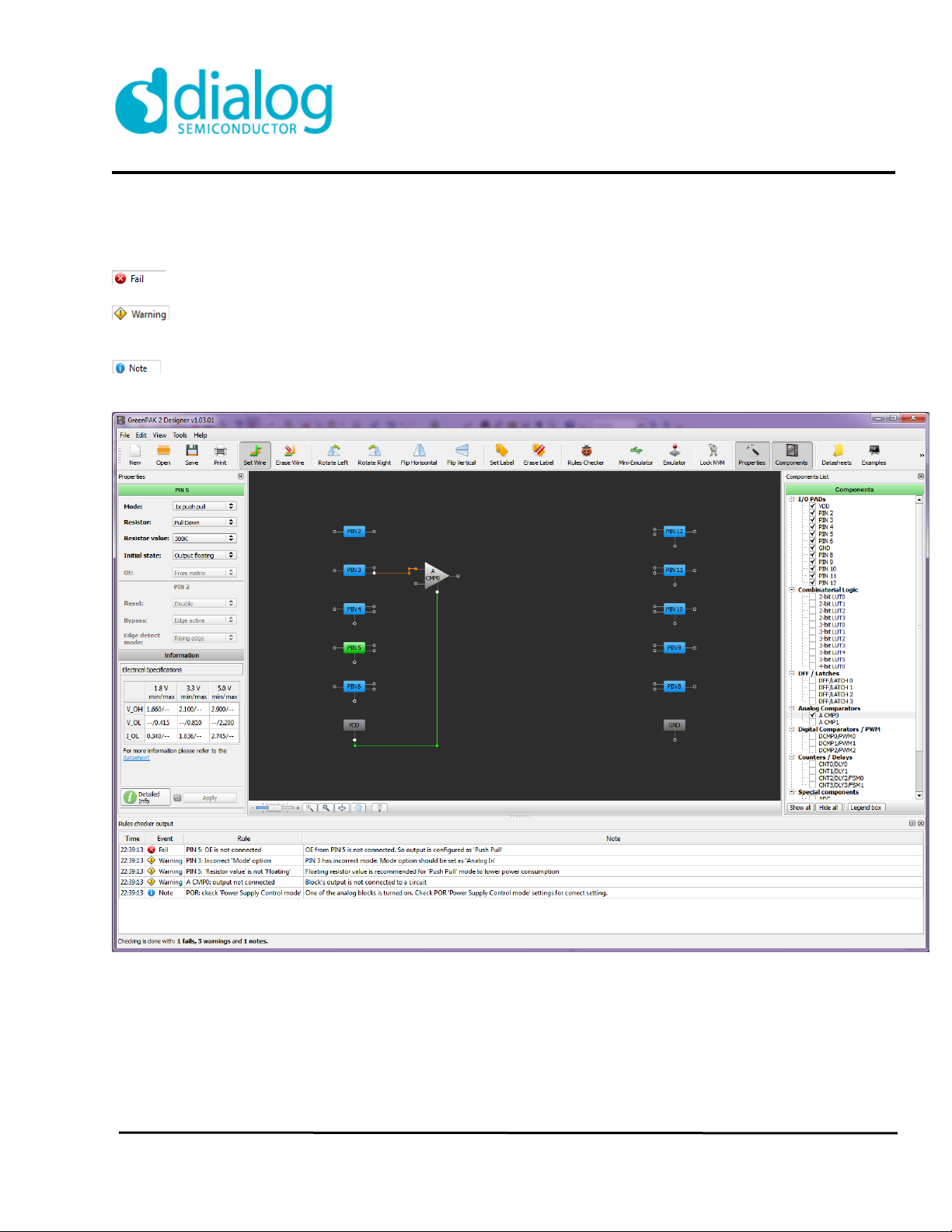
5. Rules Checker
This tool allows checking current project errors, for example, incorrect block connections or settings. Rules
Checker has three types of messages:
- this message is generated when there is a significant error in design that will not work under any
conditions.
- this message is generated when one or more blocks may contain incorrect connections or settings in
the design. This does not mean that there is an error. It only notifies the user to check the connections or settings
of the blocks.
- this message is generated to remind the user to check for correct settings.
Figure 5-1. Rules Checker Output
In order to check the design, click the Rules Checker button on the tool bar in Tools menu.
Rules Checker Window can be called by clicking Rules checker output in View menu.
Rules checker output consists of three parts:
1. Event – shows message type (Fail, Warning, Note).
2. Rule – information about the message.
3. Note – recommendations on how to correct the error or error explanation.
Dialog Semiconductor www.dialog-semiconductor.com
12/24/2020 46
GreenPAK
GreenPAK Designer 6.25
Page 47
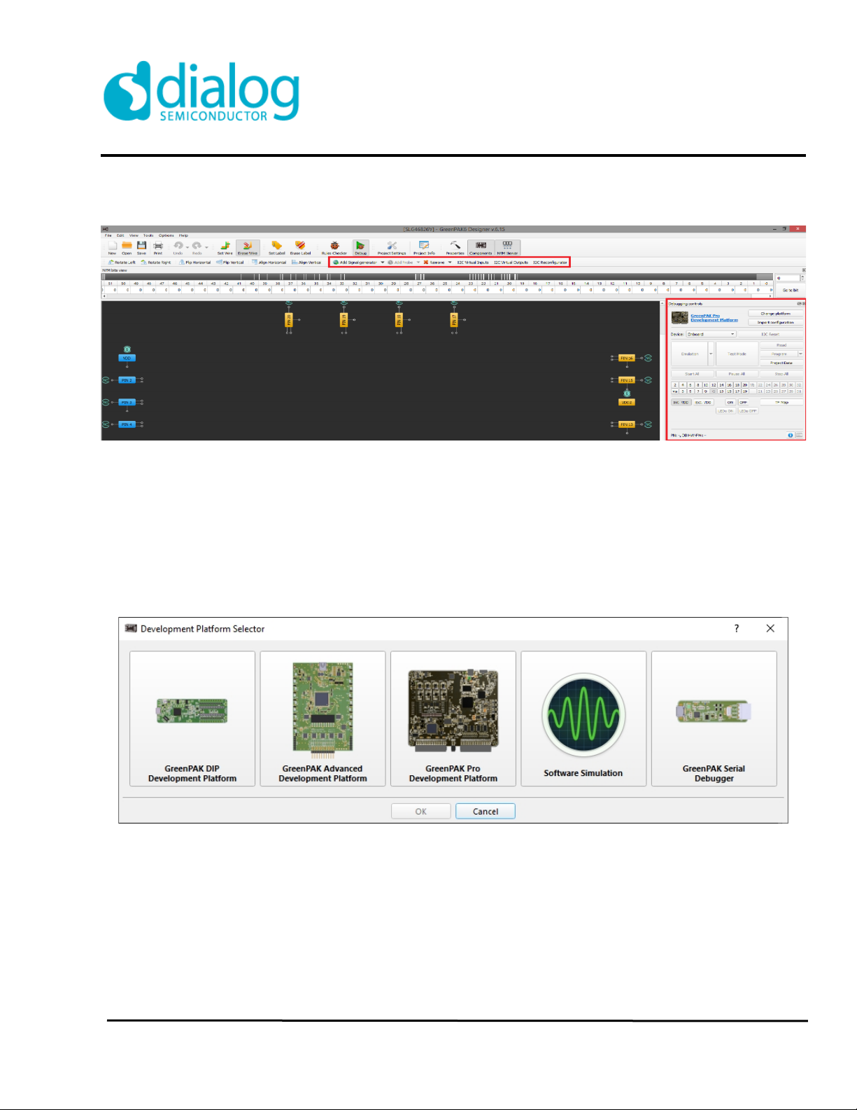
6. GreenPAK Debug Tool
Figure 6-1. Debug Panel and Debugging controls in GreenPAK Designer
Debug
Debug button starts Debug tool in GreenPAK Designer (Figure 6-1). The Debug tool enables electronic circuit
emulation and chip programming, which uses specific hardware platform to replicate the behavior of chip
components included in GreenPAK. Before starting the emulation process, add test points controls to configure
the emulation process.
Type of hardware platform
After start of Debugging tools select type of hardware platform with supported features (Figure 6-2):
Figure 6-2. Platform selector window
Dialog Semiconductor www.dialog-semiconductor.com
12/24/2020 47
GreenPAK
GreenPAK Designer 6.25
Page 48

Platfrorm Configuration Guide
Recommended Platform Configuration Guide contains information about suitable sockets, adapters and boards
for the specific chip. The user can pop up the guide by clicking on platform’s name into Debugging controls panel.
Figure 6-2. Recommended Platform Configuration Guide
Add test points controls
Debugging tool controls are used to configure input signals on external inputs of chip (proper test points on
development platform).
To manage chip input signals:
• Use the context menu on input pin with right mouse button click on NC (not connected) symbol (Figure 6-
3).
Figure 6-3. Add control context menu
Dialog Semiconductor www.dialog-semiconductor.com
12/24/2020 48
GreenPAK
GreenPAK Designer 6.25
Page 49
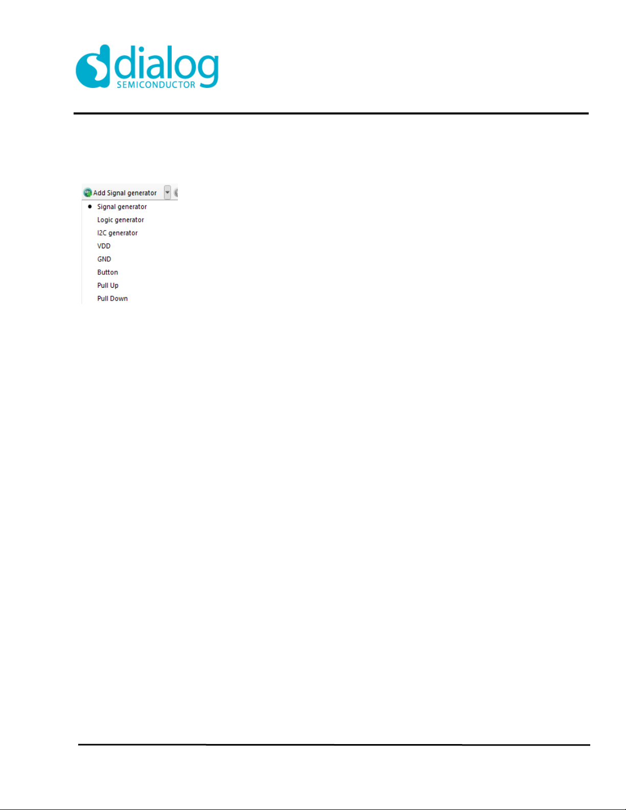
• Add control to TP with Add button on Debug panel (Figure 6-4). List of available controls on TP: Signal
generator/Logic generator/VDD/GND/Button/Pull up/Pull down.
Figure 6-4. Add button on Debug panel
Remove test points controls
Remove button removes test points controls by mouse click on it. TP become NC. Also user can set TP control as
N/C from context menu by clicking with right mouse button.
Dialog Semiconductor www.dialog-semiconductor.com
12/24/2020 49
GreenPAK
GreenPAK Designer 6.25
Page 50

6.1. Types of Areas
Fixed Inputs (Figure 6-5 – 6-9).
Figure 6-5. N/C (not connected)
Figure 6-6. Set to VDD
Figure 6-7. Set to GND
Figure 6-8. Pull Up
Figure 6-9. Pull Down
Dialog Semiconductor www.dialog-semiconductor.com
12/24/2020 50
GreenPAK
GreenPAK Designer 6.25
Page 51
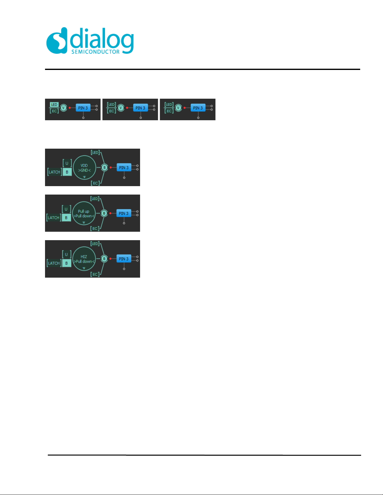
LED's (Figure 6-10)
Figure 6-10. Buffered LED, Buffered LED+Pull Up, Buffered LED+Pull Down
Configurable Input (Figure 6-11)
Figure 6-11. Configurable Button
The default connection can be set to either Upper connection or Bottom connection. Click your mouse over the
key U or B to change the value.
The user can configure each connection to VDD/GND, High-Z or Pull Up/Down.
Dialog Semiconductor www.dialog-semiconductor.com
12/24/2020 51
GreenPAK Designer 6.25
GreenPAK
Page 52

Figure 6-12. Default Key Connection
The switch has 2 modes: Latched, Unlatched, which can be configured from the context menu or click your mouse
over the key LATCH to change the value.
Figure 6-13. Key Mode
Dialog Semiconductor www.dialog-semiconductor.com
12/24/2020 52
GreenPAK
GreenPAK Designer 6.25
Page 53

User can assign Hot Key for 'Push' action. The assigned key will simulate mouse click over the key:
Figure 6-14. Choosing Hot Key
User can assign the same hot key to other Switches which allows changing the key values of all the Switches with
the same hot key at once.
Dialog Semiconductor www.dialog-semiconductor.com
12/24/2020 53
GreenPAK
GreenPAK Designer 6.25
Page 54
6.2. Generators
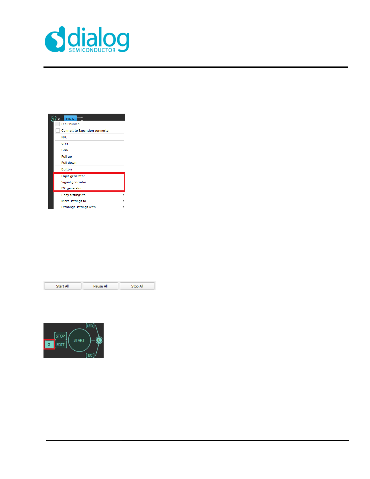
To defined TP can be connected 3 types of generators: Logic generator, Signal generator or I2C generator. User
can add generator with Add button to highlighted green pins or use context menu of the TP.
Figure 6-15. Choosing Generators
Each generator has its own settings. For the settings window to appear press the Edit button or double click on S
or L or SDA/SCL symbol at TP.
On the left, you can see the options table divided into 2 groups:
1. General – applied to all types of generators
2. Special for each generator
Start all generators with buttons at Debugging controls panel (Figure 6-16)
Figure 6-16. Managing Buttons
Note: these buttons can be controlled only by generators with an installed Global Linkage flag.
Figure 6-17. Global Linkage
Dialog Semiconductor www.dialog-semiconductor.com
12/24/2020 54
GreenPAK
GreenPAK Designer 6.25
Page 55

6.2.1. General Options in a Signal Wizard Mode
Figure 6-18. General Option
Generator: - generator selector
Shown period: Auto/Custom/1T/2T/3T/4T - set the period of a current
generator to be displayed
Global linkage Linked/Unlinked -if generator is linked, it will be
controlled by buttons “Start”,
“Stop” and “Pause” on the
Debugging controls
Repeat One shot/Cyclic/Custom - repeat option
Prestart state Low/Start point(V0)/High-Z -state before start
Prestart delay -delay before start
End state Keep last state/Prestart state -pin state after generation
Output type High-Z/Strong Drive/Open Drain, Drives High/
Open Drain, Drives Low/Resistive Pull Up/
Resistive Pull Down/ Resistive Pull Up/Down
- type of output
Pause type Last state/Low/High/High-Z -state when it is paused
Dialog Semiconductor www.dialog-semiconductor.com
12/24/2020 55
GreenPAK
GreenPAK Designer 6.25
Page 56
6.2.2. Period Modes
AUTO Mode
All generators with 'AUTO' option have one scale; this scale = MAX period of all generators with 'AUTO' option.
Figure 6-19. One Scale for All Generators
Dialog Semiconductor www.dialog-semiconductor.com
12/24/2020 56
GreenPAK
GreenPAK Designer 6.25
Page 57

Figure 6-20. User Can Change the Scale Manually
button turns on/off the mouse coordinates in the timing diagrams.
Dialog Semiconductor www.dialog-semiconductor.com
12/24/2020 57
GreenPAK
GreenPAK Designer 6.25
Page 58

CUSTOM Mode
Figure 6-21. Choosing Period Options
Dialog Semiconductor www.dialog-semiconductor.com
12/24/2020 58
GreenPAK
GreenPAK Designer 6.25
Page 59

6.2.3. Logic Generator
Figure 6-22. Logic Generator
Logic generator is used for generating the logic pulses.
Figure 6-23. 'Edit' button allows configuring the signal.
Configuration options:
Mode: Normal/Invert - signal mode
Pattern: 0 – low/ 1- high level - pattern of pulse levels
Repeat: One shot/Cyclic/Custom - repeat option
T/Level: - sets duration of level
Insert: - insert pulse before selected position;
Remove: - remove pulse from the selected position;
Levels count: - pulse count
Dialog Semiconductor www.dialog-semiconductor.com
12/24/2020 59
GreenPAK
GreenPAK Designer 6.25
Page 60
6.2.4. I2C Generator
Figure 6-24. I2C Generator
I2C generator allows a user to make an I2C signals based on logic generators. There are two logic generators
combined together as SDA and SCL lines. User can combine predefined I2C primitives to generate the needed
waveform in an appropriate way and choose SCL frequency.
SCL
Generates SCL signal applicable for I2C. SCL signal is the special kind of logic generator applicable only for
board configuration. SCL is only 'read-only'. The SCL clock configured by choosing predefined frequency. The set
of those frequencies depends on the development platform.
SDA
Generates configured SDA signal applicable for I2C. SDA signal is the special case of logic generator applicable
for sending data via I2C. In Signal Wizard special editor shows sequence of commands. User can do some
actions in command editor:
• change SCL pin for selected SDA;
• change Speed of I2C clock;
• control resource meter;
• сhange Slave Address for all commands in list;
• сlear list to basic commands: Start and Stop;
• add or remove commands by using +/- buttons;
• change command parameters;
• split Composite commands in sequence of Basic commands by using button “S”;
Figure 6-25. I2C Generator commands editor
Dialog Semiconductor www.dialog-semiconductor.com
12/24/2020 60
GreenPAK
GreenPAK Designer 6.25
Page 61
Figure 6-26. 'Edit' button or double click on SDA/SCL allows configuring the signal.
Configuration options:
SCL: Any available pin - selects pin to be the I2C clock channel
with defined frequency
Speed: 1-1000kHz - speed of I2C clock
Used resources: % - shows used resources after adding
commands to list
Change Slave Address hex - changes slave address in all commands
Clear - clears all commands from the list to Start
and Stop
Commands - list of I2C generator commands
Dialog Semiconductor www.dialog-semiconductor.com
12/24/2020 61
GreenPAK Designer 6.25
GreenPAK
Page 62

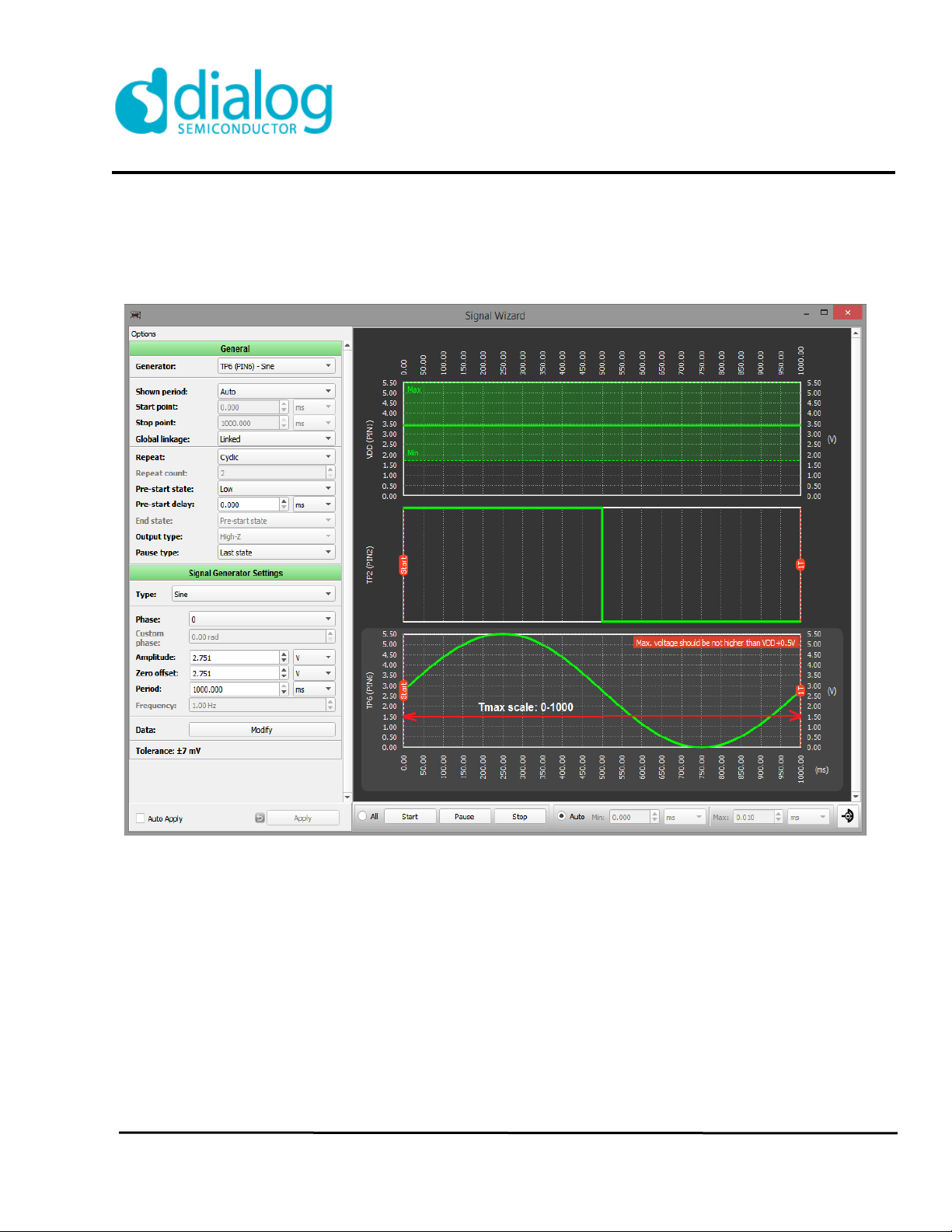
6.2.5. Signal (Analog) Generator
Figure 6-27. Signal Generator
Signal generator is used to generate analog signals: Constant Voltage level, Sine, Trapeze(Trapezoid), Logic
pattern and User-defined.
Logic and signal generators can be started/paused/stopped using orange buttons or through the context menu.
The user can also assign the hot keys for start/pause.
More than one generator can use the same hot button to start/pause at once. This is how to start more than one
generator at the same time.
Figure 6-28. Sets Start/Pause Hot Key
Dialog Semiconductor www.dialog-semiconductor.com
12/24/2020 62
GreenPAK
GreenPAK Designer 6.25
Page 63

Signal Generator Settings
Type: Const voltage level/Trapeze/Logic pattern/Sine/Custom - type of waveform;
Constant value:
U:
- voltage level;
Figure 6-29. Constant Value
Dialog Semiconductor www.dialog-semiconductor.com
12/24/2020 63
GreenPAK
GreenPAK Designer 6.25
Page 64

Figure 6-30. Sine
Sine settings:
Repeat: One shot/Cyclic/Custom - repeat option
Phase: Custom/0/Pi:2/Pi/3Pi:2 - φ0
Custom phase:
- show phase in a radian
Amplitude: - amplitude
Zero offset: - zero offset
Period: - period
Frequency:
- shows frequency
Data: - change signal using Custom Signal Wizard
Dialog Semiconductor www.dialog-semiconductor.com
12/24/2020 64
GreenPAK
GreenPAK Designer 6.25
Page 65

Figure 6-31. Trapezoid (Triangle, Sawtooth)
Trapeze Settings:
Mode: Normal/Invert -signal mode
Umax/Umin -max/min voltage level
T1, T2, T3, T4 -duration of trapezoid
If T3 = 1 signal is a triangle.
If T3 = 1, T2 = 2 or T4 = 2 signal is a saw.
Dialog Semiconductor www.dialog-semiconductor.com
12/24/2020 65
GreenPAK
GreenPAK Designer 6.25
Page 66

Figure 6-32. Duration of Trapezoid
Dialog Semiconductor www.dialog-semiconductor.com
12/24/2020 66
GreenPAK
GreenPAK Designer 6.25
Page 67

Figure 6-33. Logic pattern
Configuration options:
Mode: Normal/Invert - signal mode
Levels adjustment: Standard/Custom - sets standard Umax/min for all levels or
U for each level
Umax/min: - Umax/min for all levels
Pattern: 0 – low/ 1- high level - pattern of pulse levels
Repeat: One shot/Cyclic/Custom - repeat option
T/Level: - sets duration of level
Insert: - insert pulse before selected position;
Remove: - remove pulse from the selected position;
Count: - pulse count
Dialog Semiconductor www.dialog-semiconductor.com
12/24/2020 67
GreenPAK
GreenPAK Designer 6.25
Page 68
Figure 6-34. Custom Signal (Arbitrary waveform)
Custom Signal Settings:
Repeat: One shot/Cyclic/Custom - repeat option;
Data: Set Signal - change signal using Custom Signal Wizard
Dialog Semiconductor www.dialog-semiconductor.com
12/24/2020 68
GreenPAK
GreenPAK Designer 6.25
Page 69

6.2.6. Custom Signal Wizard
Figure 6-35. Drawing Signal (Arbitrary waveform)
Toolbar: Clear - clear data
Add Point/Add Peak/Continuous
Ramp/Remove Point
- draw mode
Data panel - turn on/off the data table
Import points - copy points from another
application
Lock X/Y - lock point position for X or Y
axes
Close - close window with current
signal
Dialog Semiconductor www.dialog-semiconductor.com
12/24/2020 69
GreenPAK
GreenPAK Designer 6.25
Page 70

Figure 6-36. Peak
Figure 6-37. Continuous Ramp
Dialog Semiconductor www.dialog-semiconductor.com
12/24/2020 70
GreenPAK
GreenPAK Designer 6.25
Page 71
Remove Point: Removes selected point. Double-clicking on the point will also remove it.
Data panel: Turns on/off the data table. User can remove/change values for selected point or add new point
between two existing points.
Figure 6-38. Import Points
User can insert points from another application and set separators options:
Decimal separator: point/comma;
Column separator: auto/tab(“\t”)/other;
Row separator: auto(line feed)/ tab(“\t”)/other;
Figure 6-39. Data Panel
Dialog Semiconductor www.dialog-semiconductor.com
12/24/2020 71
GreenPAK
GreenPAK Designer 6.25
Page 72
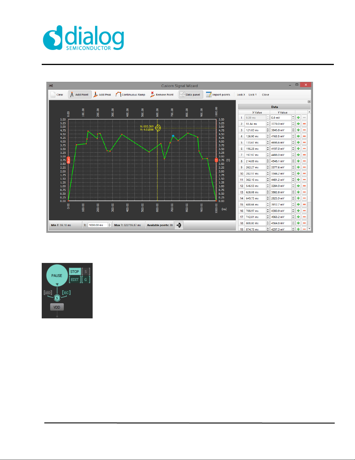
Figure 6-40. Cursor
6.2.7. VDD/VDD2 Power Signal Generator
Figure 6-41. VDD/VDD2 Power Signal Generator
Simple signal generator for VDD/VDD2 with its own options.
The additional power supply (VDD2) on some chip revisions provides the ability to interface two independent
voltage domains within the same design. Users can configure pins, dedicated to each power supply, as inputs,
outputs, or both (controlled dynamically by internal logic) to both VDD and VDD2 voltage domains. Using the
available macro-cells designers can implement mixed-signal functions bridging both domains or simply pass
through level-translation in both HIGH to LOW and LOW to HIGH directions.
Sync Power Rails [S] mode means that VDD and VDD2 will share the same power settings. VDD2 will have the
same power options as VDD. Sync power options is available only for VDD/VDD2 power generators.
Dialog Semiconductor www.dialog-semiconductor.com
12/24/2020 72
GreenPAK
GreenPAK Designer 6.25
Page 73

6.3. Expansion Connector
User can connect/disconnect I/O pads of GreenPAK with the expansion connector on the board.
Figure 6-42. Expansion Connector
6.4. Control panel
Figure 6-43. Debugging controls
Change platform:
Select type of hardware platform with supported features
Import configuration:
Allows user import configuration of test points from another platforms.
Device:
Allows user work with external chip on specified device address
I2C Reset:
If I2C serial communication is established with the device, it is possible to reset the device to initial power up
conditions, including configuration of all macrocells, and all connections provided by the Connection Matrix. This
is implemented by setting register I2C reset bit to “1”, which causes the device to re-enable the Power-On Reset
(POR) sequence, including the reload of all register data from NVM.
Dialog Semiconductor www.dialog-semiconductor.com
12/24/2020 73
GreenPAK
GreenPAK Designer 6.25
Page 74

Emulation:
• Emulation - the current project will be loaded to the chip (but not programmed), and will be ready for test
on the hardware board.
• Emulation (sync) – in addition to Emulation, each change that is made in the project, will be immediately
loaded to the chip.
In the case when Int. VDD and VDD key on the Expansion connector are turned off, a warning message will pop
up (Figure 6-44).
Figure 6-44. Incorrect Power Configuration
Test mode:
Test mode is used for connecting or disconnecting the chip’s I/O pads to TP controls, configured by user.
Also, a user can check the programmed chip using the test mode without emulation. In order to do this: turn on
the test mode and internal VDD button. The test mode can work without power on the chip. User will control the
power manually.
Read:
Read chip using hardware board.
Program:
Program chip with the current project. For some chip models user can configure programming process by clicking
Programming options at Program button. Choose programming options:
• Program NVM - programs chip NVM;
• Program EEPROM - programs chip EEPROM;
Project Data:
The table of NVM and EEPROM(optionally for some chip) bits.
Pattern ID – gives an ID (1-255) to the project. The ID will be put in the chip after programming, and also will be
read back while in “chip reading” operation.
Lock status – blocks NVM reading/writing. A programmed project becomes unavailable for chip reading/writing.
Use current project’s sequence for Programming and Emulation process – user can choose to use current
project's sequence for programing and emulation process.
Use this sequence for Programming and Emulation process – user can choose current sequence for
programming and emulation process.
Reload from current project – user can load bit sequence from current project.
Clear – sets all bits to false.
Export – save data to text file.
Import – load data from text file.
Open in new Designer's window – open current bit sequence in new Designer’s window.
Dialog Semiconductor www.dialog-semiconductor.com
12/24/2020 74
GreenPAK
GreenPAK Designer 6.25
Page 75

Figure 6-45. Project Data
In GreenPAK Designer for chips with I2C Serial Communication new columns describes register flags in I2C tools
and NVM Data window:
- I2C Legend:
• Green – Supported;
• Red - Not supported;
• Yellow - Partly supported (operation is supported for some part of data block);
- I2C Operations:
• R - I2C Read;
• W - I2C Write;
Dialog Semiconductor www.dialog-semiconductor.com
12/24/2020 75
GreenPAK
GreenPAK Designer 6.25
Page 76
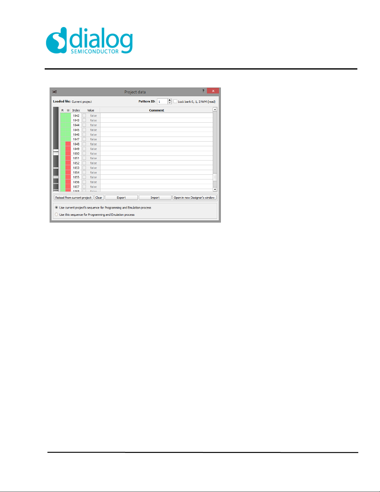
Figure 6-46. I2C operations in NVM Data window
Chip Details:
Show details about chip and board
Log:
Show log.
Dialog Semiconductor www.dialog-semiconductor.com
12/24/2020 76
GreenPAK
GreenPAK Designer 6.25
Page 77

Test points configuration:
- Save current configuration of a test points to the project file
- Delete selected configuration
- Import new configurations from project files or platforms
Figure 6-47. Test Points Configuration
Support for multiple devices:
This feature allows user to connect few supported hardware boards and select specific one for performing the
operations.
Figure 6-48. Multiple hardware devices
Blink:
Selected board blinks to notify its selection
Refresh button:
Refresh button updates chip information in bottom right corner of the Debug tool.
Socket Test:
This feature allows testing the socket connectors to ensure that it works properly and doesn't have influence on
emulation or reading/programming processes.
Figure 6-49. Socket Test Results
Dialog Semiconductor www.dialog-semiconductor.com
12/24/2020 77
GreenPAK
GreenPAK Designer 6.25
Page 78

I2C Tools
Start Debug to start work with I2C tools:
Figure 6-50. I2C Tools in Debug tool
The I2C Serial Communication Block (I2C) in the chip allows an I2C bus Master to read and write information via
a serial channel directly to the RAM registers. This allows the remote re-configuration of macro-cells. The user
has the flexibility to read and write registers not associated with NVM memory. Those registers are the signal
outputs of macro-cells in the device, giving the I2C bus Master the capability to remotely read the current value of
any macro-cell. Up to 16 GreenPAK I2C slave devices can share the same serial bus. You can choose any
external device address and work with external chip using Device selector in Debug tool: Onboard or any of 16
GreenPAK I2C slave devices:
The I2C cell also has dedicated registers (I2C Virtual Output bits) as well as dedicated arrays in memory (RAM
Array Table) only accessible through I2C. The I2C Virtual Outputs are also signals that enter the matrix. To start
I2C Tools Emulation or Test Mode is required.
I2C Tools has 3 separate windows:
I2C Virtual Inputs:
• Counters/Delays – the counter/delay data in the device can be read and write via I2C;
• I2C Virtual Inputs – the I2C Virtual Inputs OUT0-OUT7 value in the device can be read and write via I2C;
• Registers – the current value of all device registers can be read and write via I2C;
• Log – shows log of read/write operations.
Dialog Semiconductor www.dialog-semiconductor.com
12/24/2020 78
GreenPAK
GreenPAK Designer 6.25
Page 79

I2C Virtual Outputs:
• Probes (Matrix inputs) – the current level on blocks output pins in the device can be read via I2C. User
can add probes to any pin(or to all visible pins) or remove probe(or all probes);
• Counted Data – the current count value in some counters (see Datasheet for selected chip revision) in the
device can be read via I2C.
I2C Reconfigurator
Figure 6-51. I2C Reconfigurator
I2C Reconfigurator allows user to change data dynamically on chip by sending NVM snapshots into chip.
Snapshot of the NVM sequence saves configuration of macrocells and connections between macrocells. The user
Dialog Semiconductor www.dialog-semiconductor.com
12/24/2020 79
GreenPAK
GreenPAK Designer 6.25
Page 80
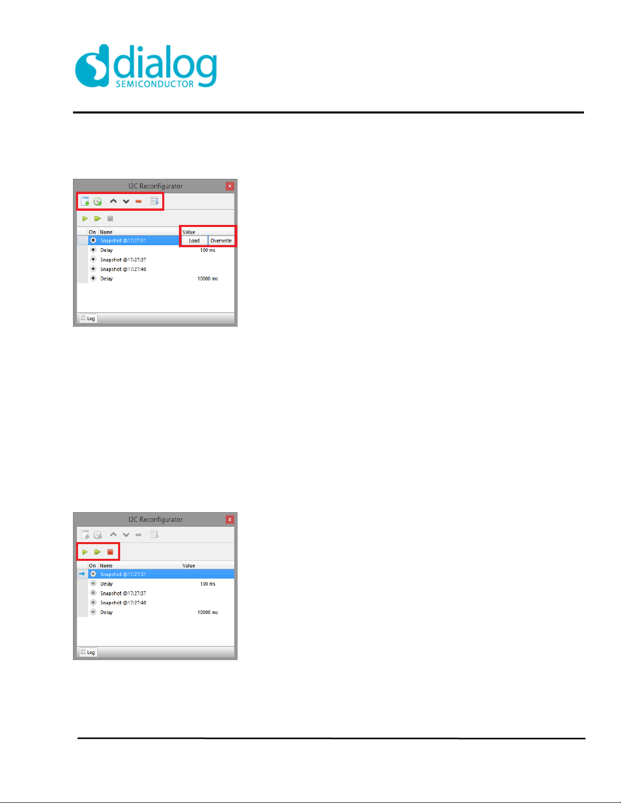
can configure list of snapshots and send into the chip in two ways: send one by one or send all. Also delays
between snapshots can be added.
Snapshot configuration:
• Snapshot – button adds snapshot of workarea to the list;
• Delay – button adds delay between snapshots to the list;
• Up – moves selected list item up one level;
• Down – moves selected list item down one level;
• Remove – removes selected list item;
• Reconfiguration scenario – shows main snapshot and it changes.
Also snapshot has value:
• Load – loads snapshot data to the project;
• Overwrite – overwrites snapshot with project data;
Snapshot operation:
• Send one – send one snapshot to the chip;
• Send all – send all snapshots from the list to the chip;
• Stop – stops sending snapshots.
Dialog Semiconductor www.dialog-semiconductor.com
12/24/2020 80
GreenPAK
GreenPAK Designer 6.25
Page 81

External chip
DIP/Advanced/Pro platforms
To start work with external chip for DIP, Advanced and PRO platforms:
1. Connect socket with External chip to Development Board via pins:
• Corresponding I2C pins (SCL, SDA);
• VDD pin;
• GND pin;
For DIP/Advanced Development board: connect socket with External chip to Expansion connectors pins:
DIP Expansion connectors:
Advanced Expansion connectors:
For PRO Development board: connect socket with External chip to external port on GreenPAK PRO Development
Board (right connector):
Dialog Semiconductor www.dialog-semiconductor.com
12/24/2020 81
GreenPAK
GreenPAK Designer 6.25
Page 82

2. Disconnect Onboard chip to proceed with the External chip (For DIP/Advanced/Pro platfroms)
3. Start GreenPAK Designer and select revision of connected External chip
4. Start Debug tool and select Development platform
5. Select Device address as 0001b (used by default for empty chip) or corresponding address programmed
to the chip.
Attention: if external socket properly connected to development board and proper Device address selected - chip
detects after clicking Update chip info button or automatically after starting any chip operation:
6. Now user can use all Debugging chip controls: Emulation/Test mode/Read/Program for external chip
Attention: Ext. VDD (Va) expansion should not be enabled if exist voltage on external VDD port. It automatically
disconnects while starting Emulation/Test mode operations for chip with existing external voltage with warning
message.
Dialog Semiconductor www.dialog-semiconductor.com
12/24/2020 82
GreenPAK
GreenPAK Designer 6.25
Page 83
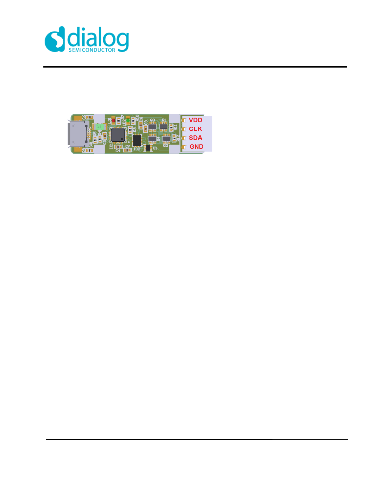
Serial Debugger
To start work with external chip on Serial Debugger platform:
1. Connect chip with wires to Serial Debugger pins (VDD, CLK, SDA, GND):
2. Start GreenPAK Designer and select revision of connected External chip
3. Start Debug tool and select Serial Debugger platform
4. Select Device address as 0001b (used by default for empty chip) or corresponding address programmed
to the chip or select
5. Specify VDD configuration: Internal (chip will be powered from Serial Debugger board) or External (chip
should be powered from external power source)
6. Now user can use all Debugging chip controls: Emulation/Test mode/Read/Program on Serial Debugger
platform
Dialog Semiconductor www.dialog-semiconductor.com
12/24/2020 83
GreenPAK
GreenPAK Designer 6.25
Page 84
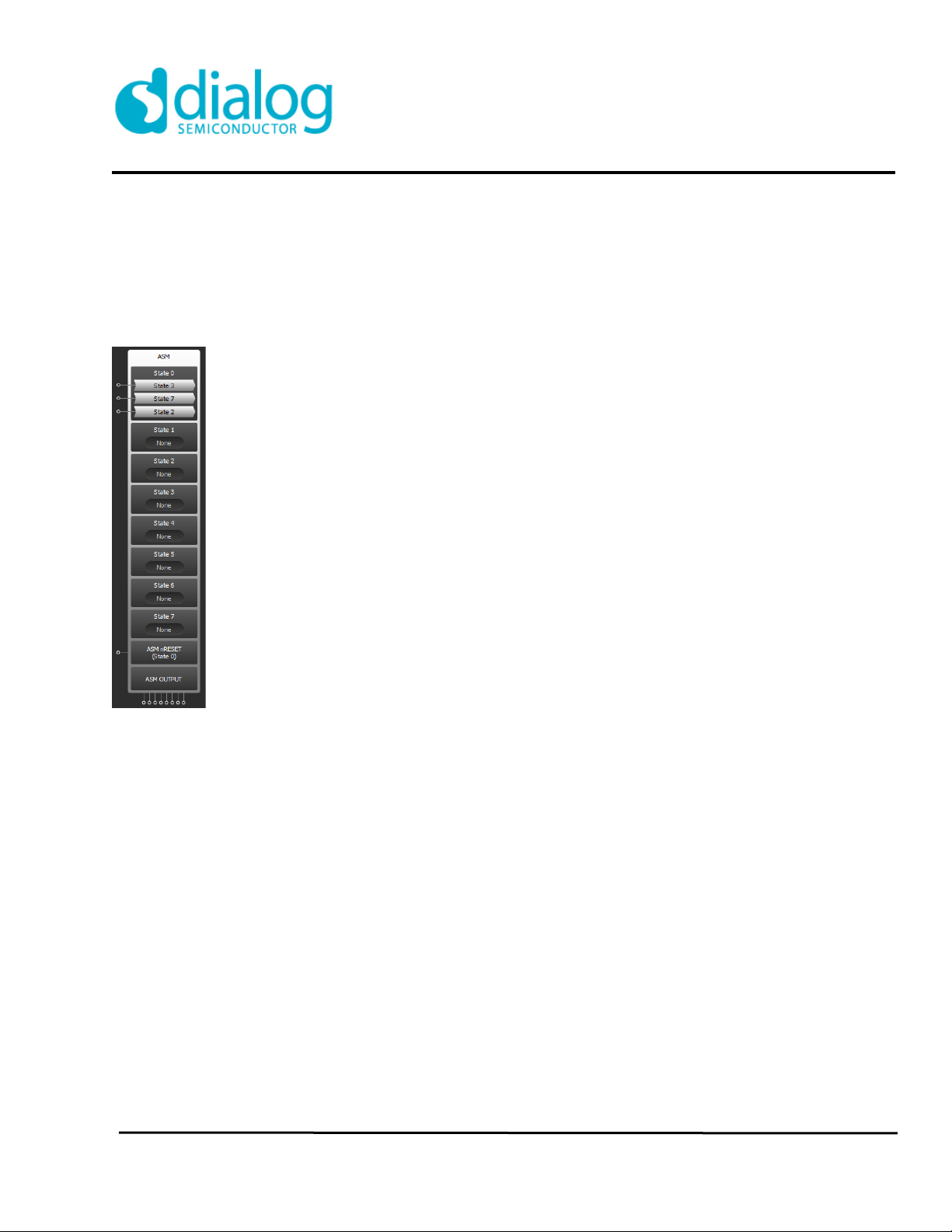
7. Asynchronous State Machine (ASM)
7.1 ASM block
The ASM block is an 8-state asynchronous state machine. There are 24 state transition inputs, one nRESET
input, and 8 output lines. The ASM block is defined using state transitions and state outputs.
Figure 7-1. ASM block.
Transitions
The state machine is constructed by defining the one-way connections between two states gated by a transition
control input. The state machine will transition to another state any time these two conditions are met: the current
state has a transition connection to another state, and that transition enable signal is HIGH. The transition enable
signals are controlled by the 24 inputs, and there are 3 transition enable signals per state.
Outputs
The ASM block has 8 outputs to the connection matrix. You can define the output of the 8 outputs based on the
current state. This is done in the properties tab by double clicking the desired output for a given state and output
line to invert its output.
Editing the ASM block
The ASM block can be defined through either the properties panel on the left, or the ASM editor. The ASM editor
is a graphical interface for defining the ASM and editing labels. Double-click on any ASM component to open ASM
Editor.
In the properties tab, you can select a state, edit its name, and configure all of its transition enable switches. Also,
you can define the ASM Outputs, edit the label names for each output, and set the Initial/reset state. In the context
menu of ASM block you can split ASM block to separate states blocks and to separate transitions (figure 7-2).
Dialog Semiconductor www.dialog-semiconductor.com
12/24/2020 84
GreenPAK
GreenPAK Designer 6.25
Page 85

Figure 7-2. Split ASM block to States/Transitions.
Initial/reset state
The ASM block will power up to the state defined as the Initial/reset state. It is by default State 0, but can be
changed to any state. It also defines which state the ASM will be reset to. When the logic on nRESET is LOW, the
ASM will be kept at the Reset state until the logic at nRESET goes HIGH.
7.2. ASM Editor
ASM editor(figure 7-3) allows to configure the ASM block using state diagram and set the output configuration for ASM Output block ASM configuration should be applied using Apply button on the toolbar to be set to the NVM.
States
State colors:
• Green: regular state;
• Blue: selected state;
• Red: initial (reset) state;
• Gray: state connections limit reached;
Move
State can be moved by dragging it’s central part using left mouse button. Dragging the border circle will have no effect.
Context menu
• Edit name: set state’s name;
• Initial state: sets current state as initial;
• Hide: hides current state.
Transitions
Add/remove links
• To create new link turn on 'Set Link’ mode and click on the border circle of source state, then click
anywhere on state-destination or 'Esc’ to cancel;
• To erase link - turn on 'Erase Link’ mode and click on the link which should be erased.
Edit shape
Link’s shape sets automatically after states change their position. Modifying of the existing shape is available in two ways:
• Simple edit: one-point editing by dragging the link;
• Flexible edit: two-points editing by entering in 'Edit path’ mode using link’s context menu;
Dialog Semiconductor www.dialog-semiconductor.com
12/24/2020 85
GreenPAK
GreenPAK Designer 6.25
Page 86
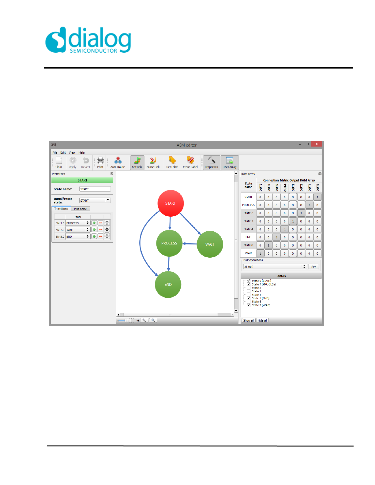
Context menu
• Set Label: sets the text label onto link;
• Erase Label: removes the text label;
• Edit path: flexible two-point editing of link’s shape.
Figure 7-1. ASM Editor.
Dialog Semiconductor www.dialog-semiconductor.com
12/24/2020 86
GreenPAK
GreenPAK Designer 6.25
Page 87

8. GreenPAK Simulation
Simulation Tools in GreenPAK Designer:
Figure 8-1. Software Simulation Tools.
Software Simulation
The Software Simulation mode enables electronic circuit simulation, which uses mathematical models to replicate
the behavior of chip components included in GreenPAK and some external components. To start Software
Simulation click on Debug button and select Software Simulation in Development Platform Selector. Before
starting the analysis, use Schematic Library and Add Probes to configure the simulation environment parameters
as shown on Figure 8-2.
Figure 8-2. Basic Simulation Tools
Dialog Semiconductor www.dialog-semiconductor.com
12/24/2020 87
GreenPAK
GreenPAK Designer 6.25
Page 88

Add Components from Schematic Library
Figure 8-3. Schematic Library
Click on component to add it to external I/O pin on chip (Figure 8-3). Voltage source(s) and GND added to
corresponded pins in chip by default. Components cannot be added to any internal macrocell. All components can
be configured from Properties panel after select or by double click on it as on Figure 8-5.
Component connects to external I/O pins with Set Wire tool. All available connections are highlighted with green
color as on Figure 8-4.
Figure 8-4. Add wire to External Component
Dialog Semiconductor www.dialog-semiconductor.com
12/24/2020 88
GreenPAK
GreenPAK Designer 6.25
Page 89
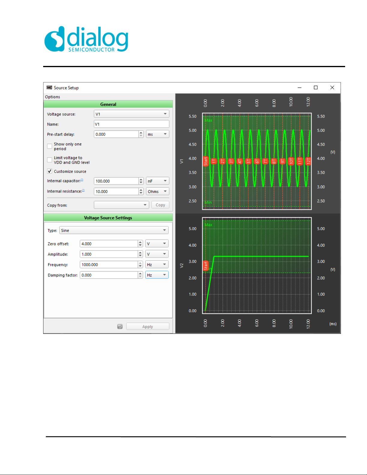
Figure 8-5. Voltage Source Setup Window
Dialog Semiconductor www.dialog-semiconductor.com
12/24/2020 89
GreenPAK
GreenPAK Designer 6.25
Page 90

General
Voltage source Source selector
Name Custom source name
Pre-start delay Delay before start
Show only one period Shows one period of voltage source
Customize source:
Internal capacitor
Internal resistance
Copy from Copy parameters from any voltage source
Voltage source settings
Type DC, Trapeze, Sine, Exponential,
Custom signal, Logic pattern, Clock
generator
- type of waveform
Please see for the reference the voltage source settings in Emulation tool (Chapter 8, 10)
Add Probe Button
Adds probes to block outputs which shows simulation results graphs over time. Probes are used to capture the
output signal from specific node. Probes can be added to the output from any pins, as well as the outputs for any
internal resource. User can add probes to all visible pins from context menu.
Remove Button
Removes probe by mouse click on it or all probes from context menu.
Dialog Semiconductor www.dialog-semiconductor.com
12/24/2020 90
GreenPAK
GreenPAK Designer 6.25
Page 91

Simulation pins configuration:
- Save current configuration of pins to the project file
- Delete selected configuration
- Import new configurations from project files of the same chip revision
Simulation Debugging controls
Select Analysis Type before starting Simulation. There are 2 types of Software Simulation: Transient and
Parametric DC.
Transient Analysis
Transient Analysis settings in Debugging controls window define period of time for simulation, maximum time
step, source voltage and temperature (Figure 8-6). Note: If there is a change in the state of any probes, there will
be a step generated at that time, the “Maximum time step” variable will only insure that if no probe data changes
for this period, another step will be generated.
Figure 8-6. Transient Analysis Window
Dialog Semiconductor www.dialog-semiconductor.com
12/24/2020 91
GreenPAK
GreenPAK Designer 6.25
Page 92
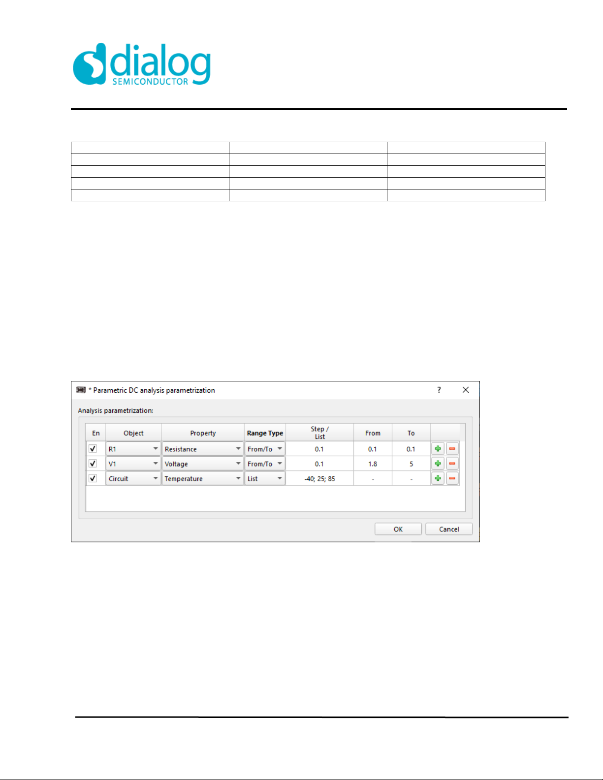
Transient analysis parameters:
Parameter Max time value Min time value
Ending time 1000s 0.0001ms
Maximum time step 20s 0.0001us
VDD 6V 0.001mV
Temperature (oC) -40 +85
Parametric DC Analysis
Customize Schematic Library objects properties by using Parametric DC analysis in Software Simulation.
Parameter sweep can be configured in the Parametric DC analysis parametrization dialog. Open parametrization
settings button on the Debugging Controls. Analysis parametrization can vary active parameters for external
components, circuit temperature, and some GreenPAK macrocell properties (e.g. Resistance (initial data) for
Digital Rheostats)(Figure 8-7). Parametric DC data has 2 range type:
• From/To: Step, From, To parameters;
• List: list of values separated by semicolon;
Figure 8-7. Parametric DC Analysis Window
Dialog Semiconductor www.dialog-semiconductor.com
12/24/2020 92
GreenPAK
GreenPAK Designer 6.25
Page 93

Parameter Probes
Figure 8-8. Parameter probes window
Parameter Probes gives ability to monitor the internal chip values in simulation, f. e. counted value in
Counter/Delay blocks. Add parameter probe by selecting component and property (Figure 8-8) and start
simulation.
Estimated completion time
Software estimates the run time in three broad categories: green, yellow and red, based on sample points. As a
general rule, green runs will complete quickly (less than 10 secs), yellow runs within one min, and red takes
longer. Run time also varies based on the speed of your computer so the estimated times vary widely. Longer run
times will also require greater resources on your computer, including CPU and memory resources.
Note that it is possible to define simulation runs that will exceed the available resources on your computer, which
can potentially make your computer unstable. This may be true any time the estimated run time is categorized as
“red”.
To start simulation, set Analysis Type, required parameters and click Start simulation. After simulation performed,
user will see Simulation results (Figure 8-9).
Dialog Semiconductor www.dialog-semiconductor.com
12/24/2020 93
GreenPAK
GreenPAK Designer 6.25
Page 94

Simulation Results Window
Figure 8-9. Simulation Results Window
The simulation result window has section:
1. Plot Widget: displays the waveforms;
2. Groups List: contains a list of all captured signals (probes) and source generators in groups;
Add group: contains a list of signals that currently are displayed on Plot widget.
a. User adds the signal from Groups section to the custom group to display it.
b. It calls ‘Groups’, because each waveform after adding to the Group section becomes a group of 1
waveform. User can select multiple waveforms at the same time and add them as a new group of
analog[A], digital[D] or parameter probes[B] waveforms (Figure 8-10).
3. Measurements: contains a list of measurements for added plot markers;
4. Toolbars: contains operations with plot area, waveforms style, groups management and export
waveforms/group data.
Dialog Semiconductor www.dialog-semiconductor.com
12/24/2020 94
GreenPAK
GreenPAK Designer 6.25
Page 95

Figure 8-10. Add group menu
In the Plot Widget, the user has following controls:
Action Hotkey
Pan mode Press middle mouse button
Marker A Ctrl + LMB
Marker B Ctrl + RMB
Clear all markers Esc or context menu → Clear markers
Zoom in/out X Ctrl + mouse wheel
Zoom in/out Y Shift + mouse wheel
Reset scales Context menu → Reset scales
Dialog Semiconductor www.dialog-semiconductor.com
12/24/2020 95
GreenPAK
GreenPAK Designer 6.25
Page 96
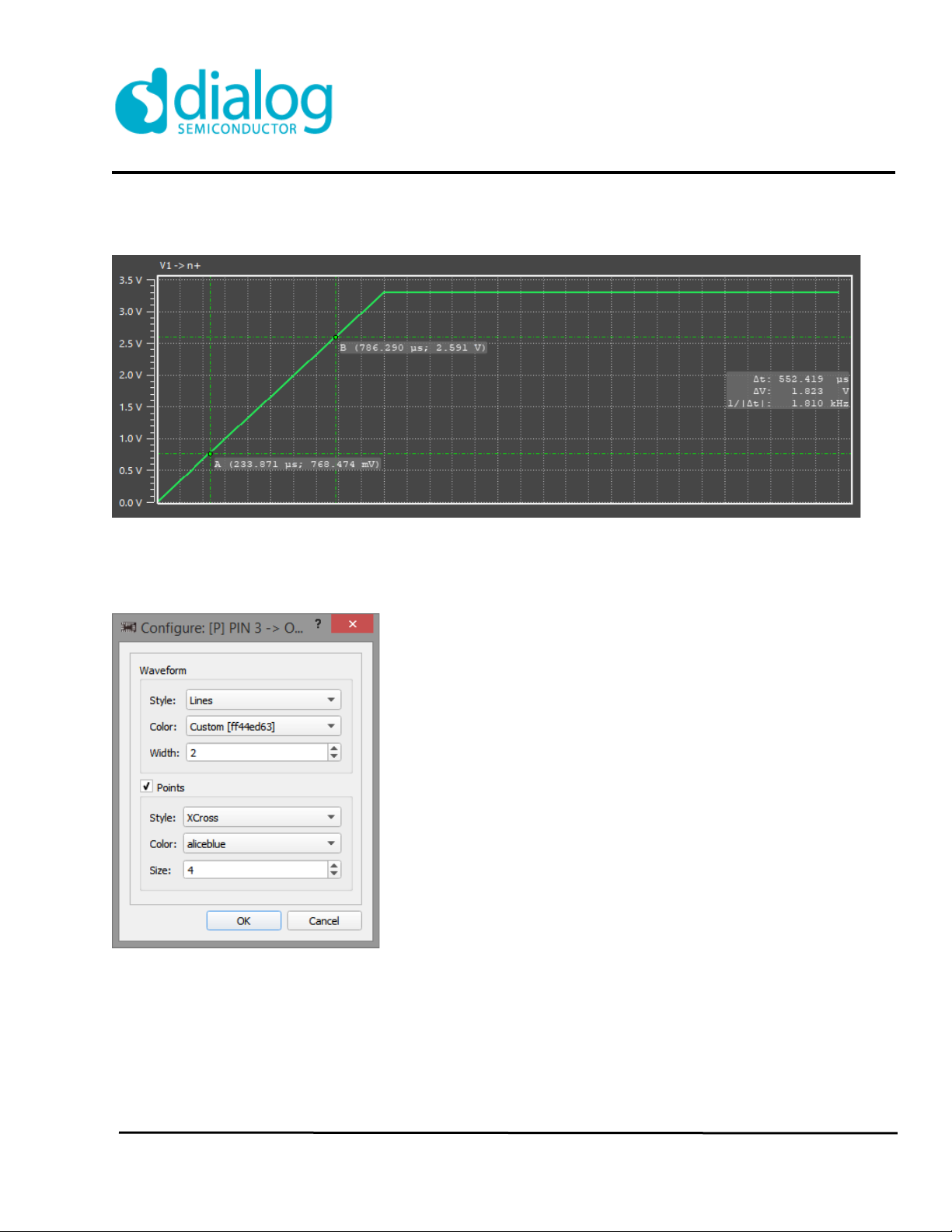
Markers and dt and dV parameters on plot widget showed in Figure 8-11 below:
Figure 8-11. Markers on Plot Widget
In Waveforms window user can configure waveforms scale and waveform base points parameters (style, color,
width/size) by clicking on Waveform style button:
Figure 8-12. Waveform Plot Configuration Window
In Groups window user has the option to:
Add group from analog[A] or digital[D] waveforms;
Remove waveforms from plot widget;
Organize order of waveforms;
Dialog Semiconductor www.dialog-semiconductor.com
12/24/2020 96
GreenPAK
GreenPAK Designer 6.25
Page 97
9. Designing Overview
9.1. SLG4672x Properties Interpretation
Pin2
Dialog Semiconductor www.dialog-semiconductor.com
12/24/2020 97
GreenPAK
GreenPAK Designer 6.25
Page 98
Dialog Semiconductor www.dialog-semiconductor.com
12/24/2020 98
GreenPAK
GreenPAK Designer 6.25
Page 99
Matrix OE IO Structure (for Pins 3, 5, 7, 9, 13, 14, 16, 18, 19)
Dialog Semiconductor www.dialog-semiconductor.com
12/24/2020 99
Only PINs 7,13,14,18,19
GreenPAK Designer 6.25
GreenPAK
Page 100

Dialog Semiconductor www.dialog-semiconductor.com
12/24/2020 100
GreenPAK
GreenPAK Designer 6.25
 Loading...