

Page 1

User manual
DA1468x/DA1510x PRO-
Development kit
UM-B-060
Abstract
PRO-Development kit consists of PRO motherboard (224-12-x) and PRO daughterboard (224-14-x
or 224-15-x)
Page 2

Contents
Abstract ..................................................................................................................................... 1
Contents .................................................................................................................................... 2
Figures ....................................................................................................................................... 4
Tables ........................................................................................................................................ 6
1. Terms and definitions ........................................................................................................... 7
2. References ........................................................................................................................... 7
3. Introduction ......................................................................................................................... 8
4. System overview .................................................................................................................. 9
Features ................................................................................................................................ 9
General description............................................................................................................... 9
5. PRO motherboard ................................................................................................................10
Overview ............................................................................................................................. 10
.................................................................... 11
PRO motherboard pin assignment ....................................................................... 13
PRO motherboard Jumper settings ...................................................................... 14
.......................................................................................... 15
.................................................................................................................... 17
....................................................................................... 18
............................................................... 19
HCI / UART header (J15) ....................................................................................... 19
Full UART configuration HCI / UART header (J15) ................................................ 20
..................................................................................................... 22
USB to UART (U12) ............................................................................................... 22
USB to JTAG (U4) .................................................................................................. 23
................................................................. 25
......................................................................................... 26
Power section ..................................................................................................................... 27
6. PRO-daughterboards ...........................................................................................................29
Overview of DA1468x/DA1510x daughterboards .............................................................. 29
Pin assignments .................................................................................................................. 32
............................................................................................................. 34
Page 3

UM-B-060
DA1468x/DA1510x PRO-Development kit
Hardware Description Manual
Revision 1.6
30-Nov-2018
3 of 56
© 2018 Dialog Semiconductor
Crystals ................................................................................................................................ 34
Battery Options ................................................................................................................... 35
Switch SW2 Settings ............................................................................................................ 37
............................................... 38
7. Known Limitations ...............................................................................................................41
Development Kit operation with only USB1 is connected .................................................. 41
Reset (older versions) ........................................................................................... 41
Charging a “0V Li-Poly battery” ............................................................................ 41
Coin Cell Battery ................................................................................................... 41
Current measurements ........................................................................................ 41
RF performance degradation in certain RF channels .......................................................... 41
RF-VCO related degradation ................................................................................. 41
RF degradation on CH14 ....................................................................................... 41
Current measurement circuit limitations ........................................................................... 41
Measuring below 1.9V .......................................................................................... 41
Full-scale measurement is voltage-depended...................................................... 42
Voltage drop due to series resistance .................................................................. 42
Calibration ............................................................................................................ 42
Fixed offset current (bleeding resistor) ................................................................ 43
Leakage when the system is powered only from VBAT ....................................... 43
8. Appendix A: Revision history ...............................................................................................44
PRO-Motherboard .............................................................................................................. 44
PRO- AQFN Daughterboard (DA1510x/DA14680x_ DB_AQFN_vD) ................................... 45
PRO- WLCSP Daughterboard (DA1510x/ DA14680x_DB_WLCSP_vE) ................................ 45
9. Appendix B: Schematic and pcb silkscreen ...........................................................................46
PRO Motherboard Schematics and pcb silkscreen ............................................................. 46
PRO AQFN60 daughterboard Schematics and pcb silkscreen ............................................ 51
PRO WLCSP daughterboard Schematics and pcb silkscreen .............................................. 51
Revision history .........................................................................................................................55
Page 4

UM-B-060
DA1468x/DA1510x PRO-Development kit
Hardware Description Manual
Revision 1.6
30-Nov-2018
4 of 56
© 2018 Dialog Semiconductor
Figures
Figure 1: PRO development kit, motherboard and daughterboard ...................................................... 8
Figure 2: PRO development kit block diagram .................................................................................... 10
Figure 3: The PCBA of PRO motherboard (224-12-E) .......................................................................... 11
Figure 4: PRO motherboard mating connectors ................................................................................. 12
Figure 5: Signals interconnection of PRO Development kit ................................................................ 14
Figure 6: Jumper’s placement on the motherboard .......................................................................... 15
Figure 7: Evaluation/debugging section .............................................................................................. 16
Figure 8: The block diagram of the debugging section ....................................................................... 16
Figure 9: RESET connectivity on PRO Motherboard ............................................................................ 18
Figure 10: Level translator schematic ................................................................................................. 19
Figure 11: HCI/UART header (J15) ....................................................................................................... 19
Figure 12: Full UART signals connectivity ............................................................................................ 20
Figure 13: Jumper’s placement for Full UART functionality ................................................................ 21
Figure 14: USB HUB circuitry ............................................................................................................... 22
Figure 15: USB to UART (U12) ............................................................................................................. 23
Figure 16: USB to JTAG (U4) ................................................................................................................ 24
Figure 17: Push button and general purpose LED schematic .............................................................. 25
Figure 18: White LED ........................................................................................................................... 25
Figure 19: The current sense circuitry ................................................................................................. 26
Figure 20: PRO development kit power components ......................................................................... 27
Figure 21: Power components location on PRO motherboard ........................................................... 27
Figure 22: VLDO linear voltage regulator, supplied from USB2 (DBG) ................................................ 28
Figure 23 : OPAMP/Analog power supply ........................................................................................... 29
Figure 24: PRO AQFN60 daughterboard top view and bottom view .................................................. 30
Figure 25: QSPI Data Flash V33 or V18 Selectable Power Supply ....................................................... 31
Figure 26: QSPI Data Flash 0 Ohms termination resistors .................................................................. 31
Figure 27: Typical CR2032 (non-rechargeable) coin cell battery ........................................................ 35
Figure 28: Recommended way of removing the coin cell battery from the battery holder ............... 35
Figure 29: Connection of the Li-Po battery ......................................................................................... 36
Page 5

UM-B-060
DA1468x/DA1510x PRO-Development kit
Hardware Description Manual
Revision 1.6
30-Nov-2018
5 of 56
© 2018 Dialog Semiconductor
Figure 30: DA1468x_AQFN_vD Daughterboard switch SW2 Setting .................................................. 37
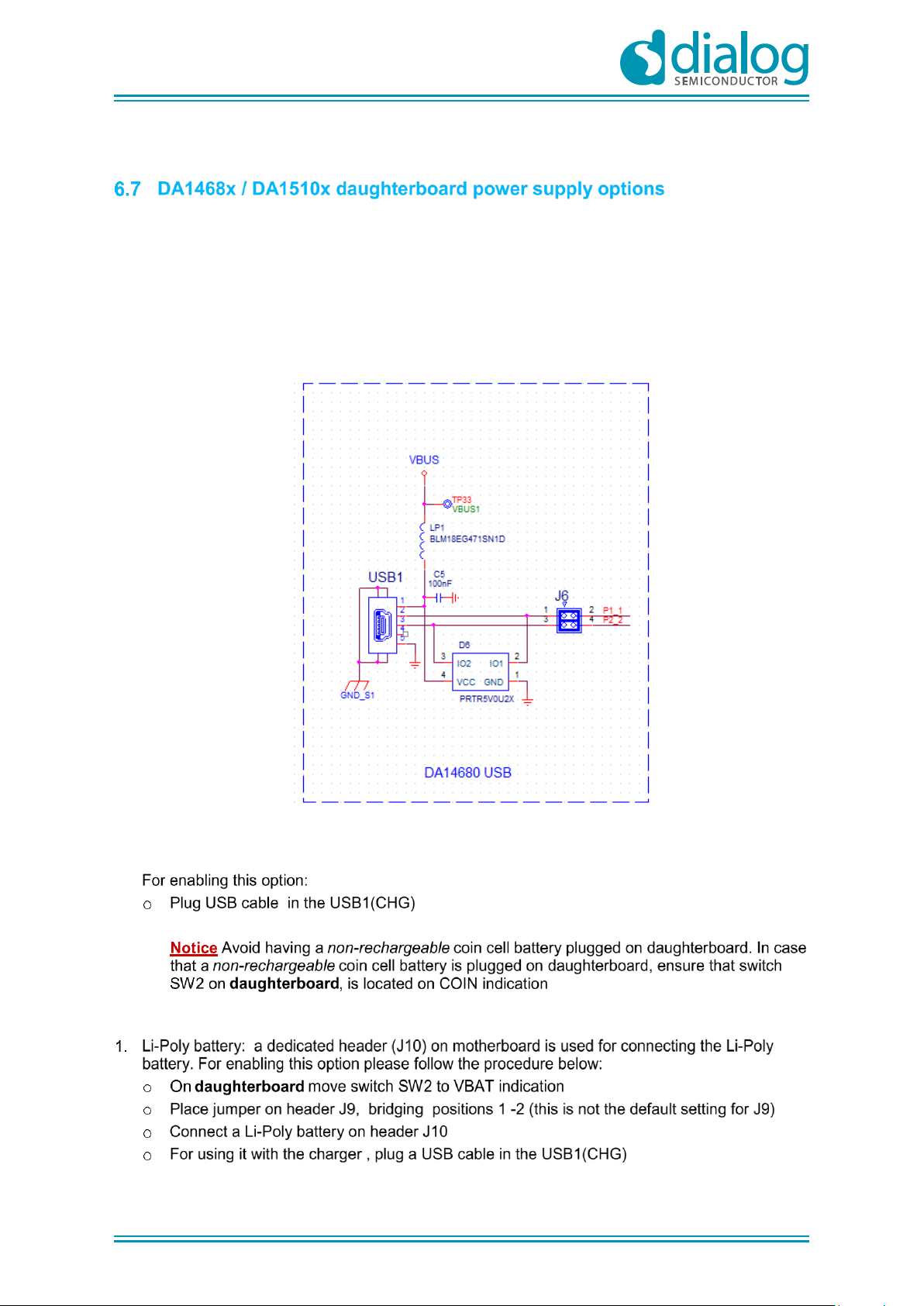
Figure 31: USB1 (CHG) port ................................................................................................................. 38
Figure 32: LiPoly battery connection diagram .................................................................................... 39
Figure 33: For enabling NTC hardware option .................................................................................... 39
Figure 34: DA1468x/DA1510x daughterboard power source selection ............................................. 40
Figure 35: VLDO (=3.0V) Power supply to RPO AQFN/WLCSP daughterboards ................................. 40
Figure 36 Shorting jumpers for lower VBAT ........................................................................................ 42
Figure 37 PowerProfiler Calibration Offset ......................................................................................... 43
Figure 38: PRO motherboard, interconnection to PRO daughterboard ............................................. 46
Figure 39: PRO motherboard, Segger ON J-link .................................................................................. 47
Figure 40: PRO motherboard, power measurement .......................................................................... 48
Figure 41: PRO motherboard, power section ..................................................................................... 49
Figure 42: PRO motherboard SILKSCREEN .......................................................................................... 50
Figure 43: PRO AQFN schematic ......................................................................................................... 51
Figure 44: PRO AQFN60 SILKSCREEN ................................................................................................... 52
Figure 45: PRO WLCSP53 SCHEMATIC ................................................................................................. 53
Figure 46: PRO WLCSP53 SILKSCREEN ................................................................................................. 54
Page 6

UM-B-060
DA1468x/DA1510x PRO-Development kit
Hardware Description Manual
Revision 1.6
30-Nov-2018
6 of 56
© 2018 Dialog Semiconductor
Tables
Table 1: PRO motherboard / daughterboard pin assignment............................................................. 13
Table 2: Jumper settings on motherboard .......................................................................................... 14
Table 3: Evaluation / debugging pins .................................................................................................. 17
Table 4: Signals using a voltage level translation/isolation chip ......................................................... 18
Table 5: DA1468x/DA1501x pin assignment of UART Signals ............................................................. 20
Table 6: Connector J1 pin assignment to WLSP/AQFN SoC ................................................................ 32
Table 7: Connector J2 pin assignment to WLSP/AQFN SoC ................................................................ 33
Table 8: Y1, 16MHz, Crystal characteristics......................................................................................... 34
Table 9: Y2, 32 KHz, Crystal characteristics ......................................................................................... 34
Table 10: PRO Motherboard revision history ...................................................................................... 44
Table 11: PRO-AQFN daughterboard revision history ......................................................................... 45
Table 12: PRO-WLCSP daughterboard revision history ....................................................................... 45
Page 7

UM-B-060
DA1468x/DA1510x PRO-Development kit
Hardware Description Manual
Revision 1.6
30-Nov-2018
7 of 56
© 2018 Dialog Semiconductor
1. Terms and definitions
BT Bluetooth
BLE Bluetooth Low Energy
PRO Professional
Devkit Development Kit
SW Software
USB Universal Serial Bus
JTAG Join Test Action Group
UART Universal Asynchronous Receiver/Transmitter
SPI Serial Peripheral Interface
LED Light Emitting Diode
LDO Low-Dropout
SOC System on Chip
2. References
Datasheet of DA14680/682, Low Power Bluetooth Smart 4.2 SoC with FLASH
Datasheet of DA14681/683, Low Power Bluetooth Smart 4.2 SoC
Datasheet of DA15100, Combo Bluetooth Smart and 802.15.4 SoC with FLASH
Datasheet of DA15101, Combo Bluetooth Smart and 802.15.4 SoC
Page 8

UM-B-060
DA1468x/DA1510x PRO-Development kit
Hardware Description Manual
Revision 1.6
30-Nov-2018
8 of 56
© 2018 Dialog Semiconductor
3. Introduction
The PRO Development kit hardware set up is described on this document. The block diagram, the
boards, the various sections, the settings as well as the connectivity is presented.
The PRO development kit consists of the PRO motherboard and the PRO daughterboard (two
variants available, AQFN60 and WLCSP). The development kit supports DA14680, DA14681,
DA14682, DA14683, DA15100 and DA15101 SoCs of Dialog Semiconductor.
Special attention for the deployment of this kit has been given in providing a trouble-free user
experience.
Figure 1: PRO development kit, motherboard and daughterboard
Page 9

UM-B-060
DA1468x/DA1510x PRO-Development kit
Hardware Description Manual
Revision 1.6
30-Nov-2018
9 of 56
© 2018 Dialog Semiconductor
4. System overview
Features
■ Highly integrated Dialog Semiconductor DA1468x/DA1510x SoC supported
■ DA1468x/DA1510x SoCs can be accessed over UART and/or JTAG with no additional external
hardware
■ Access on all GPIOs provided from the chipReset push button
■ General purpose LED and Push Button
■ White LED connected to dedicated PWM pin (LED1 pin)
■ Current monitoring circuit associated with appropriate software on PC
■ Powered from either USB2 (DBG) connector or Li-Po Battery
■ JTAG and UART interface over USB2 (DBG) connector for development purposes
■ Option for Coin-Cell battery on the daughterboard (non-rechargeable, no current monitored)
■ Dedicated USB (USB1-CHG) connector for charging a Li-Po battery
■ DA1468x/DA1510x different package easily replaceable by replacing the daughterboard
■ QSPI flash on daughterboard for DA14681, DA14683 and DA15101
■ 2.4GHz printed inverted-F antenna on the daughterboard
■ RF mechanical switch for conducted RF measurements on the daughterboard
■ Breakout headers with clearly marked signals
■ 16 MHz system and 32.768 KHz low-power crystals on the daughterboard
■ Fixed 3.0V/1.8V and a variable (1.9 to 4.3V) LDO power options
General description
The PRO development kit consists of the motherboard (Pro motherboard) and the PRO
daughterboard (two variants available, AQFN60 and WLCSP):
• PRO motherboard with board number: 224-12-E
• AQFN60 daughterboard, with board number: 224-14-D
• WLCSP daughterboard with board number: 224-15-E
Individual daughterboards are populated with each different version of SoC. For DA14681,
DA14683 and DA15101 an external Flash is populated and there are daughterboard options with
the SOC in aQFN-60 or WLCSP-53 package. For DA14680, DA14682 and DA15100 no external
Flash is populated and these are available only in the aQFN-60 package.
Page 10

UM-B-060
DA1468x/DA1510x PRO-Development kit
Hardware Description Manual
Revision 1.6
30-Nov-2018
10 of 56
© 2018 Dialog Semiconductor
DA1468x/DA1510x
U1
Vbat1
Vbat2
USB2
(DBG)
UART to USB
(FTDI), U12
JTAG to USB
(SEGGER), U4
H
U
B
U11
Vbus
Dp/Dm
SW2
SENSE
daughterboard
QSPI
vddioq
32KHz
16MHz
Break-out Headers
LDO
3.0V
D1
White Led
D2
LED
161
RESET
K2
HCI
LED1
P1_5
UART
JTAG
PRO- motherboard
RFIO
Jmp
K1
J10, Li-Poly
BATTERY
Connector
en
Level
Translator, U3
connectorpower
debugging
2
1
1
(GHG)
USB1
J9
BT1
Coin
P1_6
J15
J3, J4
Board
Figure 2: PRO development kit block diagram
DA1468x/DA1510x SoC is carried on the PRO daughterboard. PRO motherboard provides power
supply options to SoC, external reset, JTAG, UART, power measurements, as well as configuring
and monitoring capabilities. PRO motherboard and PRO daughterboard are the main components of
the PRO development kit.
5. PRO motherboard
Overview
Board number
• 224-12-E
Ports
• USB1 (CHG) for charging purpose
• USB2 (DBG) for evaluation and debugging purposes
Interfaces
• UART
• JTAG
Page 11

UM-B-060
DA1468x/DA1510x PRO-Development kit
Hardware Description Manual
Revision 1.6
30-Nov-2018
11 of 56
© 2018 Dialog Semiconductor
Connectivity – Expansion connectors
• AQFN/WLCSP daughterboards (J1, J2)
• Breakout headers (J3, J4)
Power source selection
• USB2 (DBG)
• Li-Poly battery
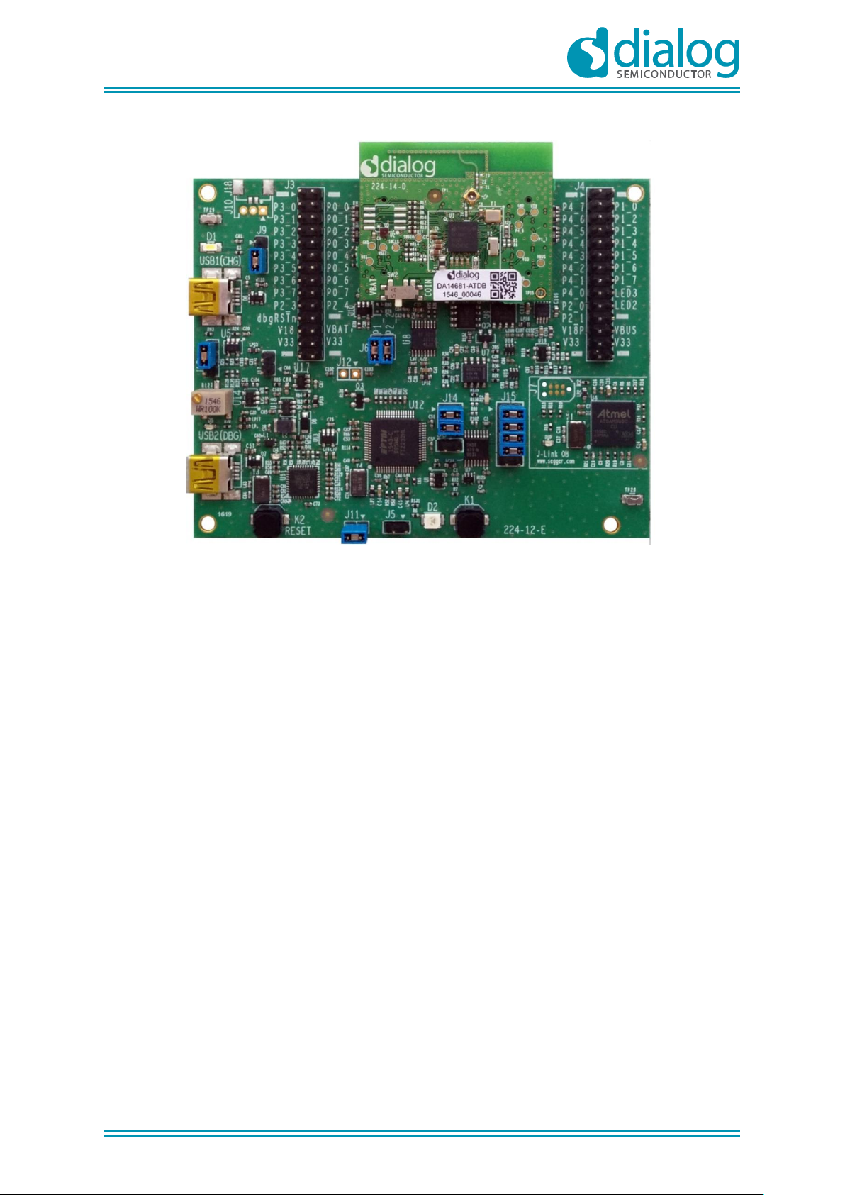
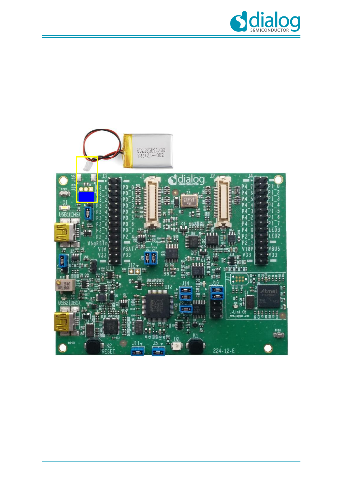
Figure 3: The PCBA of PRO motherboard (224-12-E)
PRO motherboard description can be separated into the following sections:
- Signal monitoring/interface (connector section): In this section the jumper settings are described.
- Evaluation / Debugging section: provides connectivity of the PRO Development kit to PC through
UART and JTAG ports. Only the current that is drawn from the daughterboard is monitored and its
value is fed into the PC via UART. Finally, user can reset the chip via the push button (K2).
- Power section: all power components available on the motherboard are described. Moreover,
power supplying option of the AQFN and WLCSP daughterboards is presented.
The PRO motherboard provides a detachable board interface and a pair of break out connectors.
The interface is for a daughterboard, which comes in AQFN60 and WLCSP versions:
J1/J2: interfaces with DA1468x/DA1510x daughterboards
Page 12

UM-B-060
DA1468x/DA1510x PRO-Development kit
Hardware Description Manual
Revision 1.6
30-Nov-2018
12 of 56
© 2018 Dialog Semiconductor
J3/J4: breakout connectors where DA1468x/DA1510x SoC signals can be accessed.
J4
J3
J1
J2
Break out
connectors
PRO daughterboards
Mating connectors
Figure 4: PRO motherboard mating connectors
Page 13

UM-B-060
DA1468x/DA1510x PRO-Development kit
Hardware Description Manual
Revision 1.6
30-Nov-2018
13 of 56
© 2018 Dialog Semiconductor
PRO motherboard pin assignment
On table below, the pin assignment on the connectors of the PRO motherboard is provided. There
are two columns, one for WLCSP and one for AQFN package of the DA1468x/D1510x SoCs.
Table 1: PRO motherboard / daughterboard pin assignment
Pin
name
WLCSP
AQFN60
Daughter
board
Breakout
headers
comments
P0_0
FL_CLK
J1.4
J3.4
Only for DA14681/ DA14683/DA15101
For DA14680/ DA14682/DA15100
these pins are Not Connected
P0_1
FL_D0
J1.6
J3.6
P0_2
FL_D1
J1.8
J3.8
P0_3
FL_D2
J1.10
J3.10
P0_4
FL_D3
J1.12
J3.12
P0_5
FL_CS
J1.14
J3.14
P0_6
SWDIO
J1.16
J3.16
P0_7
GPIO
J1.18
J3.18
P1_0
GPIO
J2.4
J4.4
Through header J5
P1_1
USBN
J2.31
Through header J6
P1_2
GPIO
J2.6
J4.6
P1_3
UTX
J2.8
J4.8
P1_4
URTS(out) / LED
(D2)
J2.10
J4.10
Through header J5. Only one can be
assigned
P1_5
URXTS
J2.12
J4.12
Through header J5
P1_6
UCTS(in) / BUTTON
(K1)
J2.14
J4.14
Through header J5. Only one can be
assigned
P1_7
GPIO
J2.16
J4.16
P2_0
Xtal32p
J2.23
J4.19
Through no populated resistors on
daughterboard
P2_1
Xtal32n
J2.25
J4.21
Through no populated resistors on
daughterboard
P2_2
USBP
J2.33
Through header J6
P2_3
URX
J1.19
J3.19
P2_4
SWCLK
J1.28
J3.20
P3_0
GPIO
J1.3
J3.3
Only available with aQFN
daughterboard
P3_1
GPIO
J1.5
J3.5
P3_2
GPIO
J1.7
J3.7
P3_3
GPIO
J1.9
J3.9
P3_4
GPIO
J1.11
J3.11
P3_5
GPIO
J1.13
J3.13
P3_6
GPIO
J1.15
J3.15
P3_7
GPIO
J1.17
J3.17
P4_0
GPIO
J2.17
J4.17
P4_1
GPIO
J2.15
J4.15
P4_2
GPIO
J2.13
J4.13
P4_3
GPIO
J2.11
J4.11
P4_4
GPIO
J2.9
J4.9
P4_5
GPIO
J2.7
J4.7
P4_6
GPIO
J2.5
J4.5
P4_7
GPIO
J2.3
J4.3
LED1
LED1
J1.27
Not applied on Break-out headers
LED2
LED2
J2.24
J4.20
Only available with aQFN
daughterboard
LED3
LED3
J2.22
J4.18
Page 14

UM-B-060
DA1468x/DA1510x PRO-Development kit
Hardware Description Manual
Revision 1.6
30-Nov-2018
14 of 56
© 2018 Dialog Semiconductor
PRO
daughterboard
J1 J2J3 J4
J15
SWDIO_P0_6
SWCLK_P2_4
P2_3
P2_3
P1_3
P1_5
P1_6
URX
UTX
RTS
CTS
J5
J8
K1
D2
NTC
J10
P1_4
J14
SWDIO
SWCLK
LED1
D1
J6
J11
C_TRIG
P1_1
P2_2
USBP
USBN
RN5 & RN7
RN1 & RN3
RST
10K
33Ω 33Ω
Sensor Lab Board (Optional)
PRO-Motherboard
J12
V12
V14
Jumper
Board
Header
Resistor
Figure 5: Signals interconnection of PRO Development kit
PRO motherboard Jumper settings
Table 2: Jumper settings on motherboard
header
Default Jumper
position
function
J5
1-2
P1_5 to RTS
J6
Mounted 1-2
Mounted 3-4
USB1(CHG), signals Dp/Dm are connected to
DA1468x/DA1510x
J8
1-2
P1_6 to CTS
J9
Mounted 2-3
DA1468x/DA1510x Daughterboard is supplied from 23: VLDO
1-2: Li-Poly
J11
Not mounted
Enables triggering from chip. To be used on current
sense circuitry
J12
No jumper allowed
Monitoring V12 (pin1) and V14 (pin2)
J13
Mounted 1-2
Mounted 1-2 : VLDO produces 3.0V
Mounted 2-3 : VLDO adjustable through R127
Not Mounted: VLDO produces 1.8V
J14
Mounted
JTAG connection to external PC is enabled
J15
Mounted 1-2 & 3-4
UART (TX, RX) connection to external PC is enabled.
For enabling full UART, mount 5-6 and 7-8.
J17
Not mounted
Mounted: force Power Enable of PRO motherboard
power devices (e.g., U5, U18 etc.)
Page 15

UM-B-060
DA1468x/DA1510x PRO-Development kit
Hardware Description Manual
Revision 1.6
30-Nov-2018
15 of 56
© 2018 Dialog Semiconductor
J15
J8
J14
J11
J5
J6
J12
J9
J11
J13
Figure 6: Jumper’s placement on the motherboard
Page 16

UM-B-060
DA1468x/DA1510x PRO-Development kit
Hardware Description Manual
Revision 1.6
30-Nov-2018
16 of 56
© 2018 Dialog Semiconductor
J3
Current
Sense
USB to JTAG (U4)
K1
D2
USB HUB
(U11)
USB to UART
(U12)
J4
J1
J2
Level
Translator (U3)
LED1
Figure 7: Evaluation/debugging section
U11
USB HUB
(USB2512B)
U12
USB to UART
(FT2232HL)
U4
USB to JTAG
(SAM3U2A/Segger)
Current sense
J15
AD
bus
Uart
bus
P1_3
P2_3
Swdio/P0_6
Swclk / P2_4
USB2
(DBG)
usb
bus
usb
bus
u_tx
u_rx
u_rts
u_cts
P1_5
P1_6
J1/J2
PRO Daughterboard header
reset
Key/leds
U3
Voltage
translator
(TXB106PW)
Uart
bus
Figure 8: The block diagram of the debugging section
Page 17

UM-B-060
DA1468x/DA1510x PRO-Development kit
Hardware Description Manual
Revision 1.6
30-Nov-2018
17 of 56
© 2018 Dialog Semiconductor
Table 3: Evaluation / debugging pins
Function
DA1468x/DA1510x
BREAKOUT
headers
Test
points
Pin
name
AQFN60
Pin
WLCSP
Pin
pins
UART
UART transmit (TX)
P1_3
B23
B6
J4.8
TP48
UART receive (RX)
P2_3
A35
B5
J3.19
TP50
UART RTS
P1_5
A28
B2
J4.12
TP51
UART CTS
P1_6
B12
E2
J4.14
TP52
JTAG
JTAG data (SWDIO)
P0_6
B8
F4
J3.16
TP49
JTAG clock (SWCLK)
P2_4
A14
F5
J3.20
TP54
BUTTONs
RESET (K2)
RST
A21
G1
J3.21 (inverted)
K1 (multiplexed)
P1_6
B12
E2
J4.14
LEDs
D1 (White LED)
LED1
B10
G2
TP35
(through
R5)
D2 (orange LED)
P1_5
A28
B2 TP34
D3 (Segger green LED)
TP9
D4 (USB HUB green)
TP36
D5 (U14, green)
TP41
RESET pin of Da1468x/DA1510x is driven through inverter U2, from:
- USB to JTAG chip (U4)
- USB to UART chip (U12). This option is not enabled
- An active-low signal applied to J3-21
After inversion the reset signal (RST) is driven to daughter board connector (J1)
Reset button (K2) connects the RST pin directly with V33, therefore creates a hardware reset on the
SOC regardless the state of other possible sources. This is useful in case the daughterboard is
supplied from a battery while the PRO-Motherboard is not powered at all.
Page 18

UM-B-060
DA1468x/DA1510x PRO-Development kit
Hardware Description Manual
Revision 1.6
30-Nov-2018
18 of 56
© 2018 Dialog Semiconductor
Figure 9: RESET connectivity on PRO Motherboard
DA1468x/DA1510x SoC is accessed from a PC through UART and JTAG (U12 and U4 respectively).
U12 and U4 are supplied with 3.3V. In the case that the SoC IO voltage rail is significantly less than
3.3V a miscommunication may occur, e.g. a discharged battery supplies the SoC. For avoiding this, a
voltage translation circuitry has been added.
The selected chip (TXB0106) is a 6-Bit Bidirectional Level-Shifting and Voltage Translator with
automatic direction detection.
Table 4: Signals using a voltage level translation/isolation chip
Pin name
Signal name
P0_6
SWDIO
P2_4
SWCLK
P1_3
TX
P2_3
RX
P1_5
RTS
P1_6
CTS
Page 19
UM-B-060
DA1468x/DA1510x PRO-Development kit
Hardware Description Manual
Revision 1.6
30-Nov-2018
19 of 56
© 2018 Dialog Semiconductor
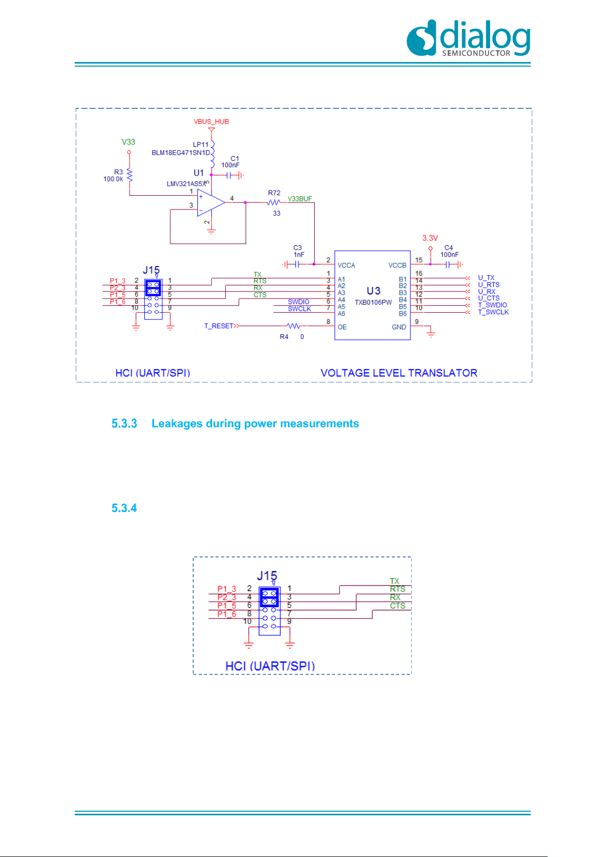
Figure 10: Level translator schematic
Current leakages occur through UART and JTAG interfaces during sleep mode. For measuring the
real power consumption during sleep modes (especially Hibernation), UART and JTAG must be
isolated from the rest of the (debugging) circuit. This is achieved by removing the jumpers from J15
and J14 for UART and JTAG respectively.
HCI / UART header (J15)
J15 interconnects DA1458x/DA1510x SoC UART signals with U12, USB to UART (FT2232HL) chip.
By removing jumpers, J15 can be used as a HCI header for other embedded hardware.
Figure 11: HCI/UART header (J15)
On-board USB/UART: by default, only TX and RX signals are connected with the jumpers placed.
RTS and CTS are multiplexed with other functions. For a full UART functionality, jumpers need to be
added between RTS – P1_5 and CTS – P1_6.
Page 20

UM-B-060
DA1468x/DA1510x PRO-Development kit
Hardware Description Manual
Revision 1.6
30-Nov-2018
20 of 56
© 2018 Dialog Semiconductor
Table 5: DA1468x/DA1501x pin assignment of UART Signals
DA1468x/DA1510x
Pin name
Signal name
Multiplexed with
functions
P1_3
TX P2_3
RX
P1_5
RTS
• LED, through J5
P1_6
CTS
• K1 push button through
jumper J8
• NTC through R89
Full UART configuration HCI / UART header (J15)
Full UART configuration is supported by enabling RTS and CTS. In this configuration:
- Jumpers in red must be placed in J15 between pin 5-6 and pins 7-8 for RTS and CTS
respectively. (Figure 12)
- Jumpers should be removed from J5 and J8. By this way signal P1_5 and P1_6 are not
connected anymore to LED D2 and key K1, respectively (Figure 12)
Figure 12: Full UART signals connectivity
Page 21
UM-B-060
DA1468x/DA1510x PRO-Development kit
Hardware Description Manual
Revision 1.6
30-Nov-2018
21 of 56
© 2018 Dialog Semiconductor
Figure 13: Jumper’s placement for Full UART functionality
Page 22
UM-B-060
DA1468x/DA1510x PRO-Development kit
Hardware Description Manual
Revision 1.6
30-Nov-2018
22 of 56
© 2018 Dialog Semiconductor
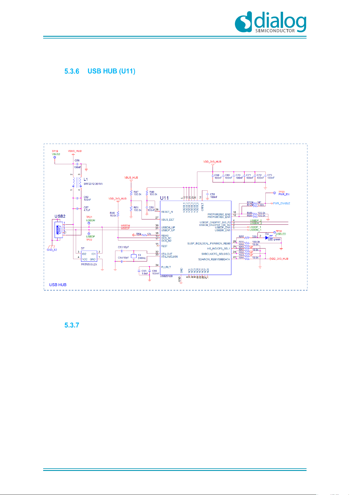
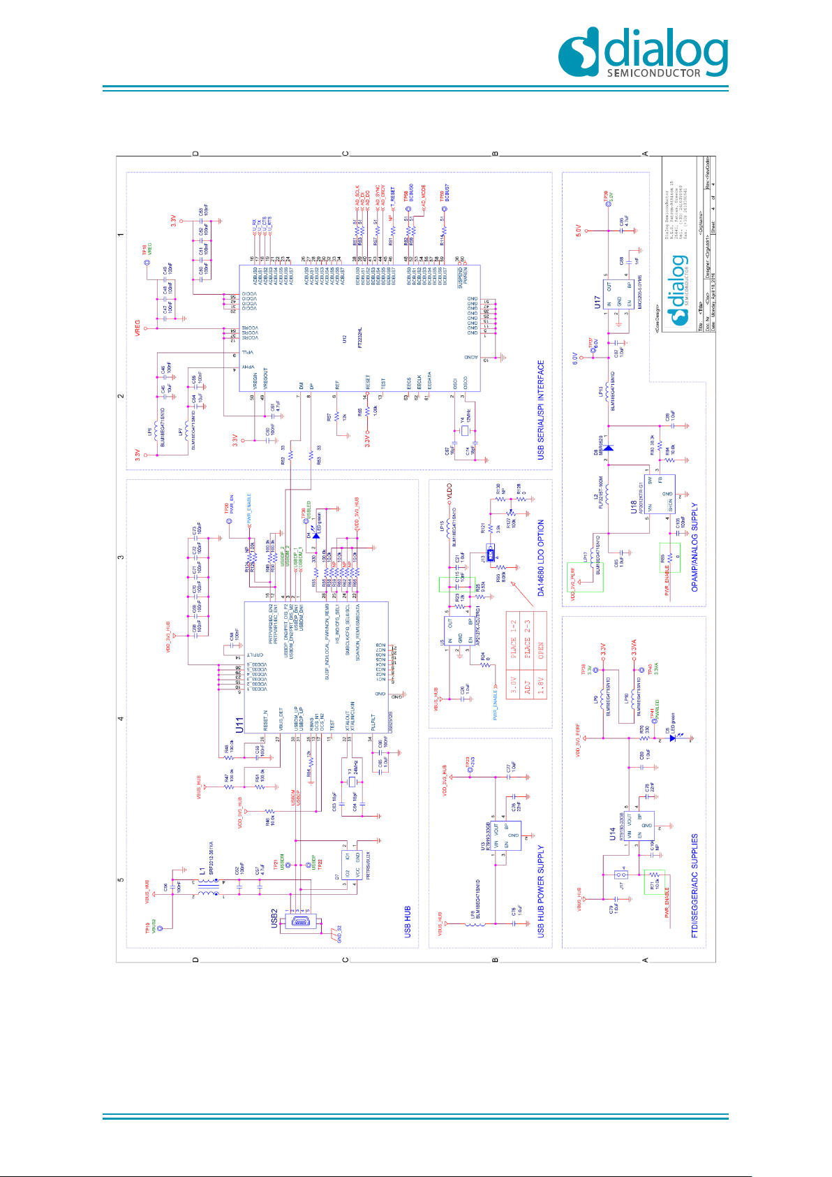
USB HUB is implemented by U11, USB2512B. This chip is supplied with 3.3V from U13.
The signal PWR_ENABLE is generated from U11 and it is an active high signal. It enables the power
components (LDOs and dc/dc converter), for UART, JTAG and current sensing circuit.
Operation is indicated via green LED D4. A 24MHz crystal (Y3) is required for the chip operation.
Figure 14: USB HUB circuitry
USB to UART (U12)
The USB to UART function is implemented by U12 FT2232HL.
Functions served by U12 are the following:
- Connectivity of PC to the DA1468x/DA1510x SoC UART port
- Connectivity of PC to current sense circuitry.
o SPI connection with ADC (U8)
o Software cursor triggering, (U_TRIG)
- Reset capability through T_RESET signal (not enabled)
The chip is supplied with a 3.3V from U14. A 12MHz crystal (Y4) is required for the chip operation.
Page 23
UM-B-060
DA1468x/DA1510x PRO-Development kit
Hardware Description Manual
Revision 1.6
30-Nov-2018
23 of 56
© 2018 Dialog Semiconductor
Figure 15: USB to UART (U12)
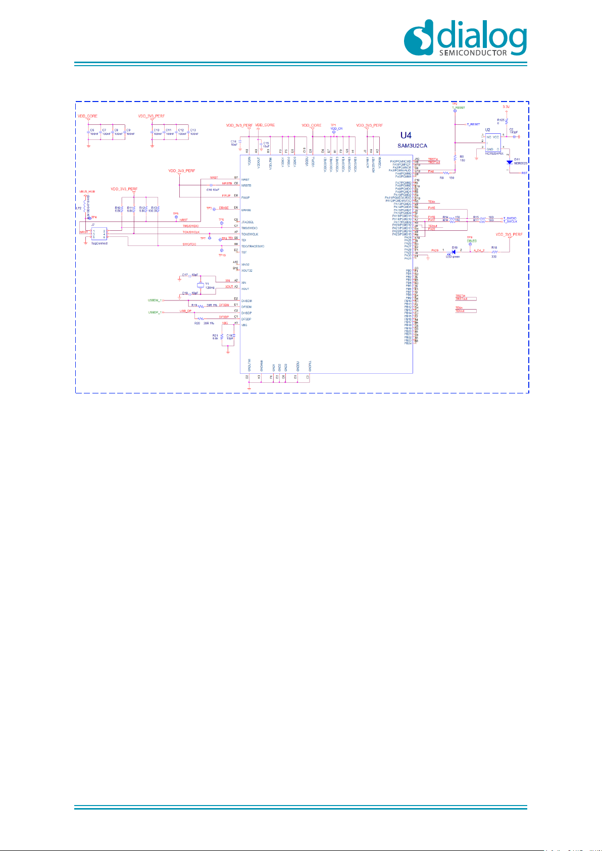
USB to JTAG (U4)
The USB to JTAG function is implemented by U4 SAM3U2CA. On the ROM of U4, software from
Segger is loaded. Functions served by U4:
- Connectivity of PC to DA1468x/DA1510x JTAG port
- Reset capability through T_RESET signal
Operation is indicated via red LED D3.
This chip is supplied with a 3.3V from U14. U14 is enabled from PWR_ENABLE signal.
TP58
BCBUS0
TP59
BCBUS7
R114 51
R61 51
AD_SCLK
R63 51
AD_DI
AD_MODE
AD_DO
R68 51
AD_SYNC
R67 51
Y4
12MHz
R81 NP
C74
18pF
C67
18pF
C55
100nF
C54
10uF
T_RESET
C46
100nF
C45
10uF
3.3V
3.3V
LP6
BLM18EG471SN1D
C48
100nF
C47
100nF
C49
100nF
VREG
C50
100nF
C51
100nF
C52
100nF
C53
100nF
R65
1.00k
AD_DRDY
3.3V
R82 51
3.3V
C61
3.3uF
C60
100nF
R52 33
R53 33
TP18
VREG
R57
12k
LP7
BLM18EG471SN1D
U12
FT2232HL
VPHY
4
OSCO
3
OSCI
2
AGND
10
DM
7
DP
8
TEST
13
VPLL
9
VCORE12VCORE37VCORE
64
VCCIO20VCCIO31VCCIO56VCCIO
42
GND1GND5GND11GND15GND25GND35GND47GND
51
ADBUS0
16
ADBUS1
17
ADBUS2
18
ADBUS3
19
ADBUS4
21
ADBUS5
22
ADBUS6
23
ADBUS7
24
ACBUS0
26
ACBUS1
27
ACBUS2
28
ACBUS3
29
ACBUS4
30
ACBUS5
32
ACBUS6
33
ACBUS7
34
BDBUS0
38
BDBUS1
39
BDBUS2
40
BDBUS3
41
BDBUS4
43
BDBUS5
44
BDBUS6
45
BDBUS7
46
BCBUS0
48
BCBUS1
52
BCBUS2
53
BCBUS3
54
BCBUS4
55
BCBUS5
57
BCBUS6
58
BCBUS7
59
VREGIN
50
VREGOUT
49
RESET
14
PWREN
60
SUSPEND
36
EECS
63
EECLK
62
EEDATA
61
REF
6
U_CTS
U_RTS
U_TX
U_RX
TO USB
HUB
(U11)
UART
To Level
Translator
(U3)
To Current Sense
Circuitry
USB SERIAL/SPI INTERFACE
Page 24
UM-B-060
DA1468x/DA1510x PRO-Development kit
Hardware Description Manual
Revision 1.6
30-Nov-2018
24 of 56
© 2018 Dialog Semiconductor
Figure 16: USB to JTAG (U4)
Page 25
UM-B-060
DA1468x/DA1510x PRO-Development kit
Hardware Description Manual
Revision 1.6
30-Nov-2018
25 of 56
© 2018 Dialog Semiconductor
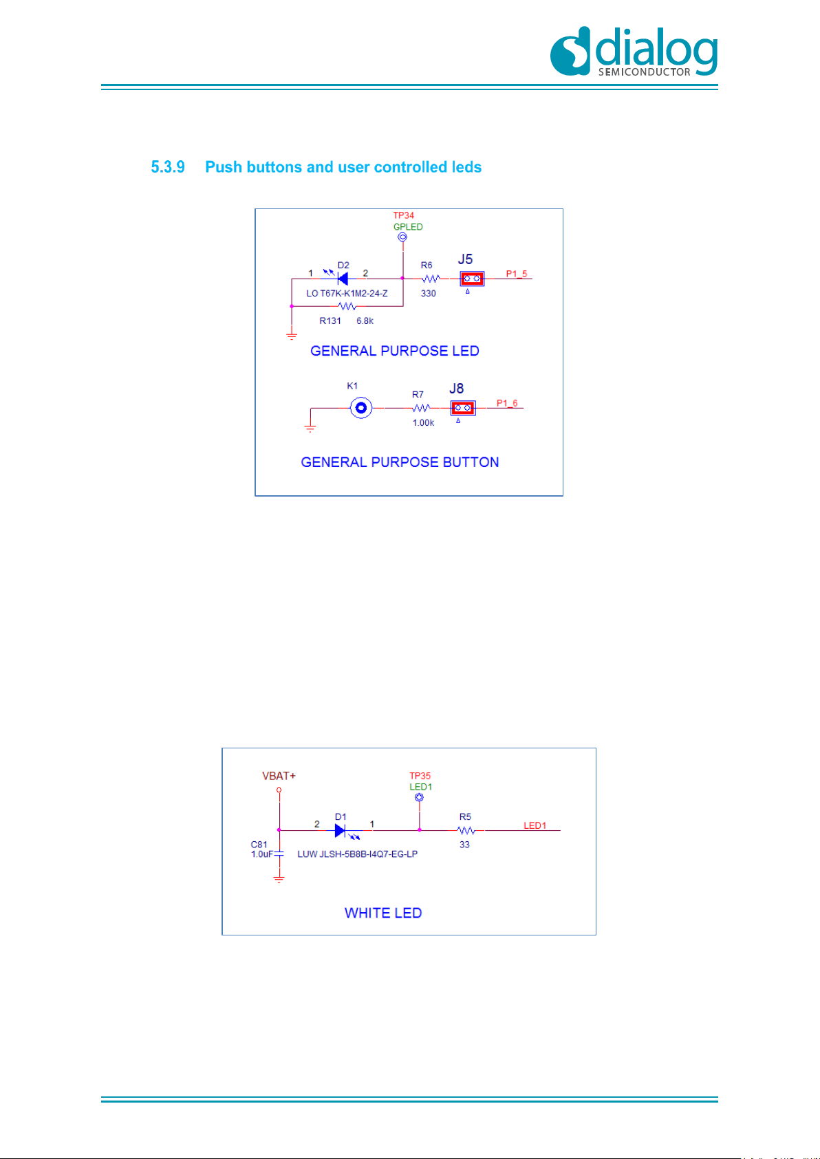
Figure 17: Push button and general purpose LED schematic
- K1 is connected to P1_6 through a jumper on header J15. Please notice that via header J13,
P1_6 is also connected to CTS.
- K2 is connected to Reset line of SoC.
- D1 (White Led): driven from LED1. LED1 is controlled directly from the DA1468x/DA1510x
SoC. LED1 is not available on the J3/J4 expanding headers.
- D2 (Orange Led): driven from P1_5 through header J14. Please notice that via header J13,
P1_5 is connected also to RTS.
Figure 18: White LED
Page 26

UM-B-060
DA1468x/DA1510x PRO-Development kit
Hardware Description Manual
Revision 1.6
30-Nov-2018
26 of 56
© 2018 Dialog Semiconductor
The supply current to PRO daughterboard (AQFN60 or WLCSP53) is monitored and measured by
the current sense circuitry. The current measurement samples are fed to PC through U4. The most
important components:
- Current sense resistor (R20=2.37 Ω, 1%) : This adds a voltage drop to the voltage supplied
to the system
- Opamp section (U6, U7, U9, U15, U16, and U17): The monitored voltage is amplified
simultaneously by U6 and U9 with a gain of 10 and 5000 respectively. U19, accompanied by
U15 and U16 decides which of the two measurements will be fed to Analog to Digital
converter. In this way, a wide range, from very low currents (sub-micro range) to higher than
100mA can be measured
- Conversion to a Differential Analog output (U7): converts signal to differential over reference
voltage and feeds this to the A/D converter (U8)
- Bleeding resistor (C100). This adds a small permanent leakage to aid in low-current
accuracy. This leakage is subtracted automatically when using the PowerProfiler software
Figure 19: The current sense circuitry
Page 27

UM-B-060
DA1468x/DA1510x PRO-Development kit
Hardware Description Manual
Revision 1.6
30-Nov-2018
27 of 56
© 2018 Dialog Semiconductor
Power section
USB1
(CHG)
USB2
(DBG)
DA1468x /
DA1510x
SoC
LDO
3.0V
LDO
3.3V
USB HUB
FTDI
SEGGER
V18/V18P
V33
SW2
PRO motherboard
J9
daughterboard
U5
U13
VBUS_HUB
VDD_3V3_HUB
LDO
3.3V
U14
VDD_3V3_PERF
OPAMP
SUPPLIES
BOOST
U18
LDO
5V
ADC
U17
VBUS
VBAT
J10
BT1
VDDIO
VBAT+
VBUS
Power_enable (from HUB)
Figure 20: PRO development kit power components
U5
USB1
USB2
U14
R127
U17
U18
U13
J10
GND
GND
Figure 21: Power components location on PRO motherboard
Page 28

UM-B-060
DA1468x/DA1510x PRO-Development kit
Hardware Description Manual
Revision 1.6
30-Nov-2018
28 of 56
© 2018 Dialog Semiconductor
Figure 22
Figure 22: VLDO linear voltage regulator, supplied from USB2 (DBG)
Page 29

UM-B-060
DA1468x/DA1510x PRO-Development kit
Hardware Description Manual
Revision 1.6
30-Nov-2018
29 of 56
© 2018 Dialog Semiconductor
Figure 23 : OPAMP/Analog power supply
6. PRO-daughterboards
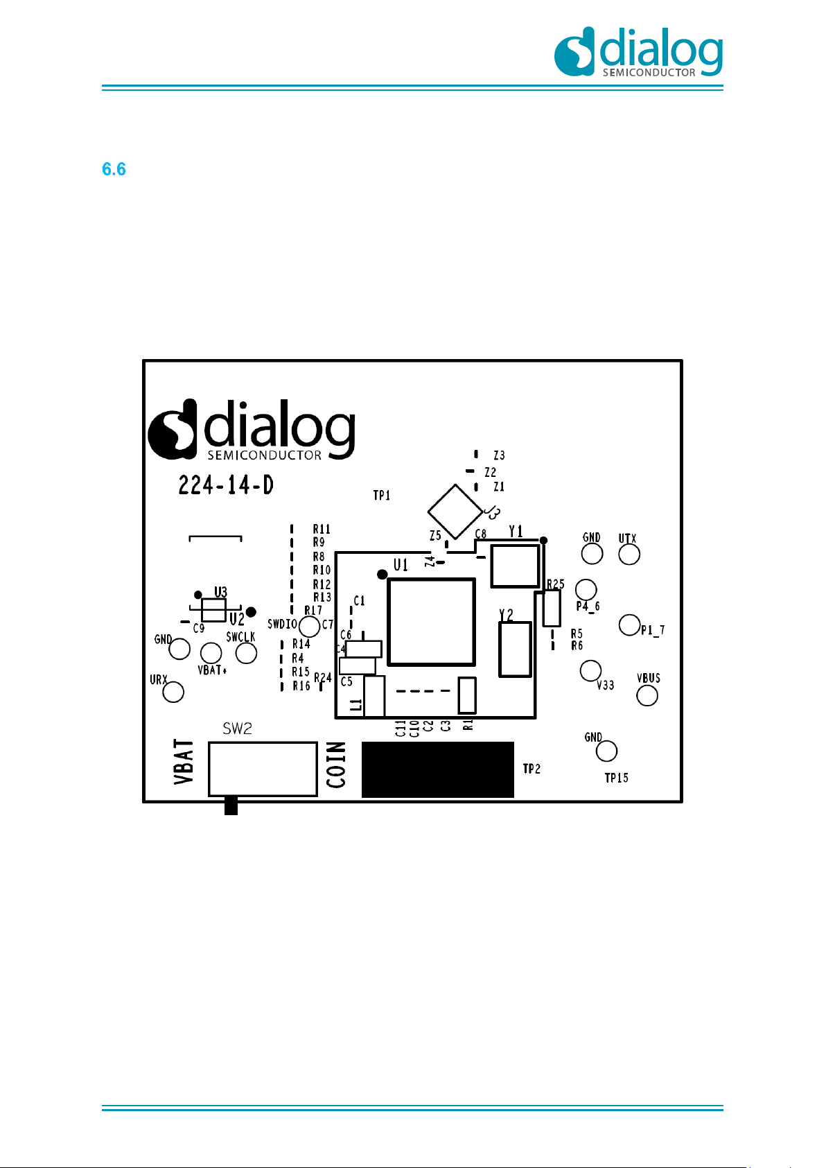
There are two daughterboards currently available:
• PRO AQFN60 daughterboard: 224-14-D
• PRO WLCSP53 daughterboard: 224-15-E
Overview of DA1468x/DA1510x daughterboards
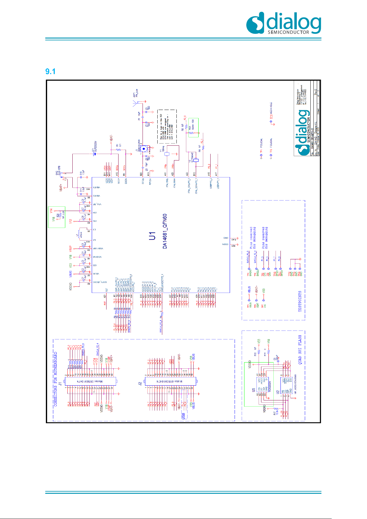
The daughterboard is designed to be used in conjunction with the PRO motherboard. Figure 24
presents PRO AQFN60 board. The basic features of the daughterboards are:
SoC
DA1468x/DA1410x AQFN60 for PRO AQFN60 / 224-14-D
DA1468x/DA1410x WLCSP53 for PRO WLCSP53 / 224-15-E
Flash Memory
• W25Q80EW (8Mbit) QSPI Flash Memory, WLCSP package - default
• W25Q16DW (16M-bit) QSPI Flash Memory, (not populated) - optional
• 1.8V power supply - default
• 3.0V power supply – optional
• Signals connected to the PRO-Motherboard through 0-ohm resistors
Clock Inputs
• 16MHz crystal
• 32KHz crystal
Two 40-pin expansion connectors
• DA14680 I/O pins as well as ground and power lines are brought out to two expansion
connectors
• The expansion connectors are placed at bottom
Coin cell holder
• Compatible with a standard CR2032 coin cell battery
Power source selection
Page 30

UM-B-060
DA1468x/DA1510x PRO-Development kit
Hardware Description Manual
Revision 1.6
30-Nov-2018
30 of 56
© 2018 Dialog Semiconductor
• Between PRO-Motherboard and coin cell battery
RF Interface
• SMD RF switch used for evaluation/ testing
• Integrated IFA antenna
• Matching network
Power selection
Mounting
connectors
Flash Termination
resistors
Coin Cell
RF
switch
QSPI
Figure 24: PRO AQFN60 daughterboard top view and bottom view
The daughterboard is plugged on top of the PRO motherboard via two low-profile 40-pin SMD
connectors which are placed at the bottom side of the PCB. Daughterboard has a mount option for a
coin cell battery holder. Power supply selection is available between the PRO-Motherboard and the
coin cell battery through switch SW2. This allows the daughterboard to operate as a standalone
device once programmed (Figure 24).
The daughterboard is also equipped with an external QSPI data flash from Winbond. The
W25Q80EW flash supports the standard Serial Peripheral Interface (SPI), Dual/Quad I/O SPI as well
as 2 clocks instruction cycle Quad Peripheral Interface (QPI), Serial Clock, Chip Select, Serial Data
I/O0 (DI), I/O1(D0), I/O2 (/WP) and I/O3(/HOLD). A 0 Ohm resistor is placed in series with QSPI
supply to allow measurements with the QSPI switched off. QSPI supply is selectable (V33 or V18)
and the same supply voltage is connected to VDDIO on DA1468x/DA1510x (Figure 25). A network of
0 ohms termination resistors is placed in series with the QSPI bus to allow isolation of QSPI data
flash from the rest of the system in case the flash is not used (Figure 26).
Page 31

UM-B-060
DA1468x/DA1510x PRO-Development kit
Hardware Description Manual
Revision 1.6
30-Nov-2018
31 of 56
© 2018 Dialog Semiconductor
Figure 25: QSPI Data Flash V33 or V18 Selectable Power Supply
Figure 26: QSPI Data Flash 0 Ohms termination resistors
The daughterboard provides an SMD RF switch and an integrated printed IFA antenna. The SMD RF
switch is used for RF evaluation/testing. The RF switch is MM8130-2600 supplied by Murata.
Verification of the circuit performance is accomplished by simply inserting an external plug in the
board mounted receptacle. This action re-directs the circuit from normal condition to the plug side.
Removing the plug restores circuit back to its normal condition. Murata offers several options for
mating plugs, MXHS83QH3000 is such an option1.
1
It is in preproduction phase and can be supplied from particular suppliers
R22
10.0k
R27 0
R26 NP
C9
100nF
P0_4
P0_0
P0_1
U2
W25Q16DWSSIG, No Pop
CS1VCC
8
DO2HOLD
7
WP3CLK
6
GND4DIO
5
DUAL QUAD SPI FLASH
VDDIO
V33
VDDIO
FL_CS
V18
P0_2
P0_3
P0_5
U9
W25Q80EWBY IG
VCC
A1
/CS
A2
/HOLD
B1
DO
B2
CLK
C1
/WP
C2
DI
D1
GND
D2
R35 0
Page 32

UM-B-060
DA1468x/DA1510x PRO-Development kit
Hardware Description Manual
Revision 1.6
30-Nov-2018
32 of 56
© 2018 Dialog Semiconductor
Pin assignments
The pin assignment of the two 40-pin connectors to the WLCSP/AQFN SoC can be seen below:
Table 6: Connector J1 pin assignment to WLSP/AQFN SoC
Connector pin
number
Signal
Name
WLCSP pin
assignment
AQFN pin
assignment
Comments
1, 2
GND 3
P3_0 A37 4
P0_0
B8
B1
FL_CLK
5
P3_1 A12
6
P0_1
A7
A2
FL_D0
7
P3_2 A10 8
P0_2
B7
A3
FL_D1
9
P3_3 A7 10
P0_3
A8
A1
FL_D2
11
P3_4 A9 12
P0_4
C8
A4
FL_D3
13
P3_5 A20 14
P0_5
C7
A5
FL_CS
15
P3_6 A22 16
P0_6
F4
B8
SWDIO
17
P3_7 B14 18
P0_7
A6
A34 19
P2_3
B5
A35
RX
20, 21
GND 22, 23
- 24
V14 25
RST
G1
A21 26
V12 27
LED1
G2
28
P2_4
F5
A14
SWCLK
29. 30
VDDIO 31, 32
GND 33, 34
V18 35, 36
V18+ 37, 38
VBAT+ 39, 40
GND
Page 33

UM-B-060
DA1468x/DA1510x PRO-Development kit
Hardware Description Manual
Revision 1.6
30-Nov-2018
33 of 56
© 2018 Dialog Semiconductor
Table 7: Connector J2 pin assignment to WLSP/AQFN SoC
Connector pin
number
Signal
Name
WLCSP pin
assignment
AQFN pin
assignment
Comments
1, 2
GND 3
P4_7 A36
GPIO
4
P1_0
C2
B15
ML8511_OUT (analog in)
5
P4_6 B22
GPIO
6
P1_2
C1
A27
I2C_SDA
7
P4_5 A33
GPIO
8
P1_3
B6
B23
TX
9
P4_4 A32
GPIO
10
P1_4
D1
A26
PDM_DATA
11
P4_3 A31
GPIO
12
P1_5
B2
A28
RTS(out)/LED
13
P4_2 B17
GPIO
14
P1_6
E2
B12
CTS(in)/BUTTON
15
P4_1 B16
SPI_CS
16
P1_7
D2
A25
PDM_CLK
17
P4_0 A24
GPIO
18, 19
- 20, 21
GND 22
LED2 A19 23
P2_0
E1
A23
Xtal32p
24
LED3 B11 25
P2_1
F1
B13
Xtal32n
26
GND 27
VBAT- 28
VBAT- 29, 30
GND 31
P1_1
F3
A17
USBN
32
- 33
P2_2
G3
A16
USBP
34
- 35, 36
GND 37, 38
V33 39. 40
VBUS
Page 34

UM-B-060
DA1468x/DA1510x PRO-Development kit
Hardware Description Manual
Revision 1.6
30-Nov-2018
34 of 56
© 2018 Dialog Semiconductor
Crystals
Table 8: Y1, 16MHz, Crystal characteristics
Reference designator
value
Part Number
7M-16.000MEEQ-T
Frequency
16MHz
Accuracy
±10ppm
Load Capacitance (CL)
10pF
Shunt Capacitance (C0)
3pF
Equivalent Series Resistance (ESR)
100 Ω
Drive Level (PD)
50μW
Table 9: Y2, 32 KHz, Crystal characteristics
Reference designator
value
Part Number
ABS07-32.768KHZ-7-T
Frequency
32.768KHZ
Accuracy
±20ppm
Load Capacitance (CL)
7pF
Shunt Capacitance (C0)
0.9 ~ 1.2pF
Equivalent Series Resistance (ESR)
70 KΩ
Drive Level (PD)
0.5μW
Page 35

UM-B-060
DA1468x/DA1510x PRO-Development kit
Hardware Description Manual
Revision 1.6
30-Nov-2018
35 of 56
© 2018 Dialog Semiconductor
Battery Options
There are two different battery types that can be used in conjunction with the pro daughterboard:
• A coin cell battery (rechargeable or non-rechargeable)
• A rechargeable Li-Po battery
Figure 27: Typical CR2032 (non-rechargeable) coin cell battery
This battery is placed at the bottom of the daughterboard in the dedicated battery holder as shown in
Figure 34. The battery needs to be inserted by sliding in first the part that will fit inside the metallic
clip of the battery holder.
However, extra attention is needed when removing the coin cell battery from its holder, if this is not
done properly then the plastic battery holder can be subject to breaking.
The recommended way of removing the coin cell battery is shown at Figure 28.
Figure 28: Recommended way of removing the coin cell battery from the battery holder
Page 36
UM-B-060
DA1468x/DA1510x PRO-Development kit
Hardware Description Manual
Revision 1.6
30-Nov-2018
36 of 56
© 2018 Dialog Semiconductor
A slotted screwdriver needs to be inserted at the point shown in Figure 28 between the metallic clip
of the battery holder and the coin cell battery itself, then by lifting the screwdriver up the coin cell
battery will pop out without damaging the plastic surroundings of the battery holder.
A rechargeable battery can also be used by following the procedure described at section 6.7.
A 3x1 through-hole male header (J10) or a two pins JST-PH Series header (J18) can be soldered on
PRO-Motherboard for connecting the Li-Po battery.
J10
Figure 29: Connection of the Li-Po battery
Page 37
UM-B-060
DA1468x/DA1510x PRO-Development kit
Hardware Description Manual
Revision 1.6
30-Nov-2018
37 of 56
© 2018 Dialog Semiconductor
Switch SW2 Settings
Same settings are applied for the two daughterboards (WLCSP and AQFN).
Switch SW2:
Move switch to indication COIN for coin cell battery selection
Move switch to indication VBAT for power supply selection
Figure 30: DA1468x_AQFN_vD Daughterboard switch SW2 Setting
Page 38
UM-B-060
DA1468x/DA1510x PRO-Development kit
Hardware Description Manual
Revision 1.6
30-Nov-2018
38 of 56
© 2018 Dialog Semiconductor
USB1 port/charger input (USB1/CHG): the SoC VBUS pin is supplied directly from the USB port.
Please notice that on this Pro Kit, only the DA1468x/DA1510x SoC is supplied from this port.
J6 connects the USB port pins to USBN (P1_1/J2.31) and USBP (P2_2/J2.33). Before hardware
Rev.E1 a value of 33 ohm was used for the USB termination resistors in series with the USB signals,
in the latest Rev.E1 these have been replaced with 0 ohm for improved compatibility with certain
USB host controllers and USB cables. It is advised for customers having a Rev.E board to replace
the USB termination resistors (R100, R101 which are located near J2) with 0 ohm.
Figure 31: USB1 (CHG) port
making sure that the charger is not
enabled
Page 39

UM-B-060
DA1468x/DA1510x PRO-Development kit
Hardware Description Manual
Revision 1.6
30-Nov-2018
39 of 56
© 2018 Dialog Semiconductor
Figure 32: LiPoly battery connection diagram
Figure 33: For enabling NTC hardware option
R89 NP
NTC
R102 NP
P1_4
P1_6
BATTERY CHARGING
Page 40

UM-B-060
DA1468x/DA1510x PRO-Development kit
Hardware Description Manual
Revision 1.6
30-Nov-2018
40 of 56
© 2018 Dialog Semiconductor
Figure 34: DA1468x/DA1510x daughterboard power source selection
Figure 35: VLDO (=3.0V) Power supply to RPO AQFN/WLCSP daughterboards
Page 41

UM-B-060
DA1468x/DA1510x PRO-Development kit
Hardware Description Manual
Revision 1.6
30-Nov-2018
41 of 56
© 2018 Dialog Semiconductor
7. Known Limitations
Development Kit operation with only USB1 is connected
Reset (older versions)
In older hardware versions of the PRO-Motherboard, before the current rev.E, the operation of Reset
function through push button K2 can’t be performed.
Charging a “0V Li-Poly battery”
Several types of Li-Poly battery are equipped with a protection circuit. The circuit protects batteries
from deep discharging, by disconnecting them from the circuit. On this state, battery presents 0V
across its terminals.
Charging a 0V Li-Poly battery when only USB1 is connected (USB2 is not connected) might not
operate, due to leakages from DA1468x/DA1510x daughterboard to debugging section of PROMotherboard. This can be avoided by removing jumpers J11, J14 and J15.
Coin Cell Battery
Current measurements
RF performance degradation in certain RF channels
RF-VCO related degradation
A loss up to 1dB in receive sensitivity can be randomly seen in channels 7,15,23,31 and 37, due to
RF VCO leakage on harmonics of the system clock (16MHz).
RF degradation on CH14
A loss up to 1dB in receive sensitivity can be observed in channel 14, due to digital noise originating
from the 27MHz oscillator on the PRO-Motherboard (the clock for the ADC converter in the current
measurement circuit).
Current measurement circuit limitations
Measuring below 1.9V
When operating DA1468x/DA1510x daughterboards with VBAT ≤ 1.9V, the power management of
SoC switches to bypass mode. In this case, a “smoothing” effect is observed on the measured
current waveforms. To avoid this, it is recommended to place additional jumpers on J3/J4, shorting
together V18/V18P/VBAT+/V33.
Page 42

UM-B-060
DA1468x/DA1510x PRO-Development kit
Hardware Description Manual
Revision 1.6
30-Nov-2018
42 of 56
© 2018 Dialog Semiconductor
Figure 36 Shorting jumpers for lower VBAT
Full-scale measurement is voltage-depended
The full scale current for voltages (VBAT) higher than 2.5V is 250mA. For voltages 2.5V to 1.7V, the
full scale is proportionally reduced. For example, for 2.1V and 1.8V supply the maximum current we
can measure is 210mA and 180mA respectively.
Voltage drop due to series resistance
The current sense resistor (2.37Ω) plus the additional resistance of PCB tracks creates a significant
voltage drop for large currents. Keep this in mind when measuring systems that handle currents
larger than the typical 20-30mA.
Calibration
A simple calibration procedure should be applied in the PowerProfiler software for each PROMotherboard, for optimum performance. The steps are:
▪ Set calibration offset on Power Profiler configuration to zero.
▪ Remove the daughterboard and any other load that may be connected to VBAT+ (on J3)
▪ Measure the current for a short period, e.g. 1 second
▪ Place the measured average value on the related Config setting “Calibration Offset (mA)”,
while negating the sign
▪ Measuring again should return an average value very close to zero
Page 43

UM-B-060
DA1468x/DA1510x PRO-Development kit
Hardware Description Manual
Revision 1.6
30-Nov-2018
43 of 56
© 2018 Dialog Semiconductor
Figure 37 PowerProfiler Calibration Offset
Please note that the calibration value depends on the voltage level of VBAT+, so repeat the
procedure after changing the voltage to a different value.
If the current needs to be measured with external ampere-meter or power source, the instrument
should be nulled, using a similar procedure.
Fixed offset current (bleeding resistor)
A resistor was added on VBAT+, in place of the unpopulated capacitor C100. This adds a small fixed
leakage, which improves the accuracy when measuring very low currents (below 10μΑ). In order to
obtain this accuracy, the offset on PowerProfiler just needs to be calibrated, as described in sd.
As the fixed leakage current depends on the supply voltage (VBAT), for the default 3.0V, it is
approximately equal to 17.24μΑ.
Leakage when the system is powered only from VBAT
In case that a daughterboard runs on a battery or external supply and it is plugged on the PROMotherboard while the PRO-Motherboard itself is not powered, a leakage of the order of 1.5mA can
be measured.
Page 44

UM-B-060
DA1468x/DA1510x PRO-Development kit
Hardware Description Manual
Revision 1.6
30-Nov-2018
44 of 56
© 2018 Dialog Semiconductor
8. Appendix A: Revision history
PRO-Motherboard
Table 10: PRO Motherboard revision history
Version
Comments
B00
Initial Release
B01
Changed R72, R79 to 33 ohm
Changed R121 to 3.9k
Changed R112, R113 to 10M
Changed R128 to 0 ohm
C00
Added space for version control label
C01
Changed LP1 to 0.56 ohm resistor
D00
Optimizations on the current measurement circuit
Changed reset button logic (so that it will work independent from
the presence of power in the support circuits)
Added D11 in series with RST (avoid leakage on RESET
pressing)
Added U20 (negative bias for U9)
D01
Changed R119 to 100k
Changed R118 to 10k
Changed C43 to 100nF
Changed C43 to 100nF
E00
Added option for battery charging analysis (not populated)
Added D12 (blue LED sleep/awake status)
Changed TP28, TP29 to 1206 probe pins (cost reduction)
Modified power input of U18 to VDD_3V3_PERF
Added C115, LDO FC cap
Added R134,TP64 (option for future expansion)
Added J18 (option for battery connector)
Modified power input of U20 to VDD_3V3_PERF
Changed LP1 part reference to R133
Changed R71 to 10k
Changed R85 to 0 ohm
Page 45

UM-B-060
DA1468x/DA1510x PRO-Development kit
Hardware Description Manual
Revision 1.6
30-Nov-2018
45 of 56
© 2018 Dialog Semiconductor
PRO- AQFN Daughterboard (DA1510x/DA14680x_ DB_AQFN_vD)
Table 11: PRO-AQFN daughterboard revision history
Version
Comments
A
Initial Release
B
Add R24=2.2K for V14 rail power at power up
Change value of C4 to 10uF
Replace SW2 pin header connector with slide switch CUS-12TB
Replace J3 RF Switch with Murata MM8130-2600
Add second choice for QSPI FLASH , U3, W25Q80EW
Replace L1 part number (L2012 , lower DC Resistance)
Change C8 from 1uF to 4.7uF
Change C3 from 10uF to 4.7uF
Connect R24 to V18 instead of VDDIO
Change pin assignment for UTX (P1_3) URX (P2_3)
C
Add Resistor R25=10MOhm to XTAL32Kp
Make Resistor R24=2.2K NP
Make W25Q80EW populated
D
Modify silkscreen to add label
Please notice that revC and revD are functionally identical. Only difference is marking.
PRO- WLCSP Daughterboard (DA1510x/ DA14680x_DB_WLCSP_vE)
Table 12: PRO-WLCSP daughterboard revision history
Version
Comments
A
Initial Release
B
Add R24=2.2K for V14 rail power at power up
Change value of C4 to 10uF
Replace SW2 pin header connector with slide switch CUS-12TB
Replace J3 RF Switch with Murata MM8130-2600
Add second choice for QSPI FLASH , U3, W25Q80EW
Change C8 from 1uF to 4.7uF
Replace L1 part number (L2012 , lower DC Resistance)
C
Connect R24 to V18 instead of VDDIO
Change pin assignment for UTX (P1_3) URX (P2_3)
D
Add Resistor R25=10MOhm to XTAL32Kp
Make Resistor R24=2.2K NP
Make W25Q80EW populated
E
Modify silkscreen for label
Please notice that revD and revE are functionally identical. Only difference is marking.
Page 46

UM-B-060
DA1468x/DA1510x PRO-Development kit
Hardware Description Manual
Revision 1.6
30-Nov-2018
46 of 56
© 2018 Dialog Semiconductor
9. Appendix B: Schematic and pcb silkscreen
PRO Motherboard Schematics and pcb silkscreen
Figure 38: PRO motherboard, interconnection to PRO daughterboard
Page 47

UM-B-060
DA1468x/DA1510x PRO-Development kit
Hardware Description Manual
Revision 1.6
30-Nov-2018
47 of 56
© 2018 Dialog Semiconductor
Figure 39: PRO motherboard, Segger ON J-link
Page 48

UM-B-060
DA1468x/DA1510x PRO-Development kit
Hardware Description Manual
Revision 1.6
30-Nov-2018
48 of 56
© 2018 Dialog Semiconductor
Figure 40: PRO motherboard, power measurement
Page 49
UM-B-060
DA1468x/DA1510x PRO-Development kit
Hardware Description Manual
Revision 1.6
30-Nov-2018
49 of 56
© 2018 Dialog Semiconductor
Figure 41: PRO motherboard, power section
Page 50

UM-B-060
DA1468x/DA1510x PRO-Development kit
Hardware Description Manual
Revision 1.6
30-Nov-2018
50 of 56
© 2018 Dialog Semiconductor
Figure 42: PRO motherboard SILKSCREEN
Page 51
UM-B-060
DA1468x/DA1510x PRO-Development kit
Hardware Description Manual
Revision 1.6
30-Nov-2018
51 of 56
© 2018 Dialog Semiconductor
PRO AQFN60 daughterboard Schematics and pcb silkscreen
Figure 43: PRO AQFN schematic
Page 52

UM-B-060
DA1468x/DA1510x PRO-Development kit
Hardware Description Manual
Revision 1.6
30-Nov-2018
52 of 56
© 2018 Dialog Semiconductor
Figure 44: PRO AQFN60 SILKSCREEN
Page 53
UM-B-060
DA1468x/DA1510x PRO-Development kit
Hardware Description Manual
Revision 1.6
30-Nov-2018
53 of 56
© 2018 Dialog Semiconductor
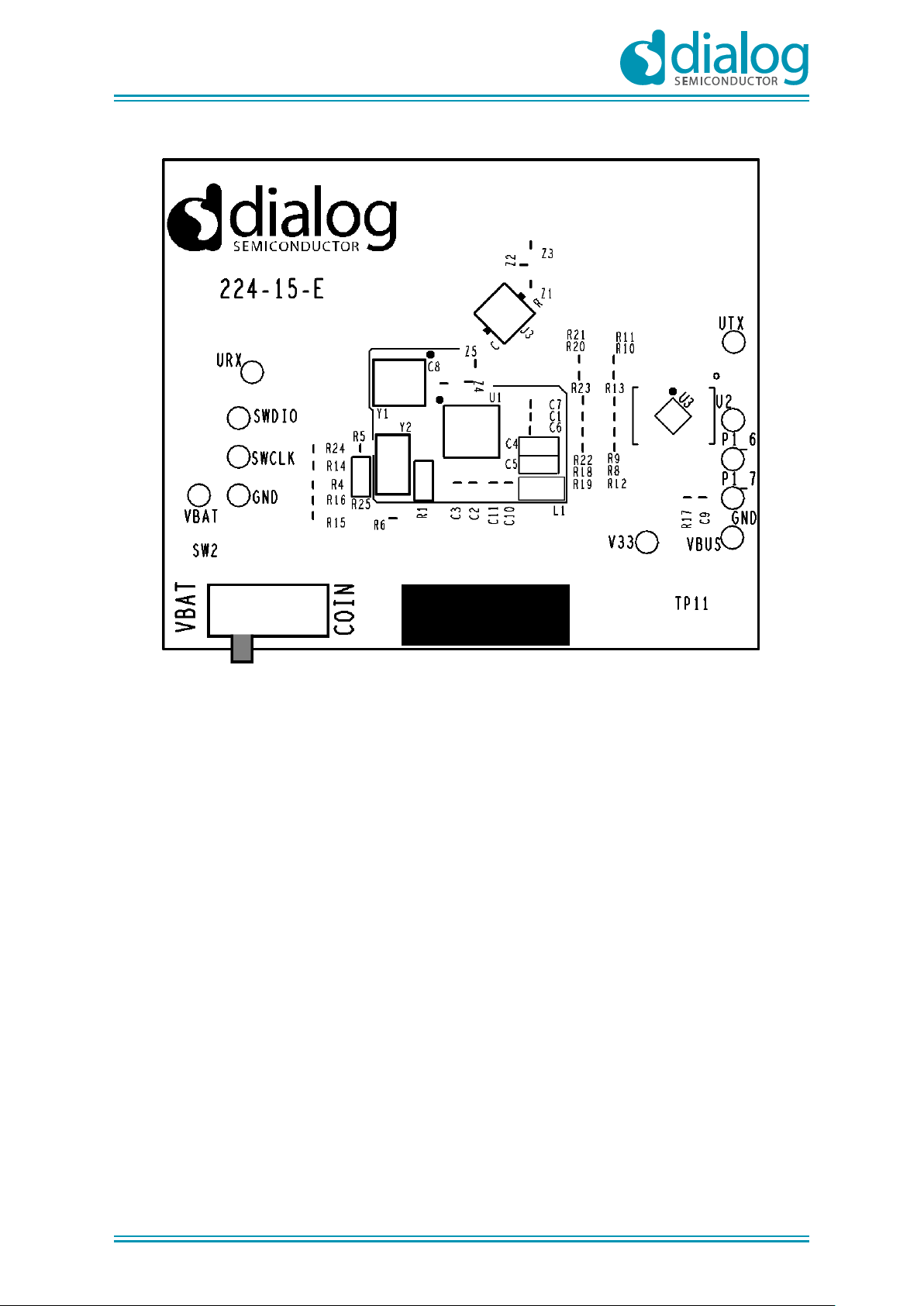
PRO WLCSP daughterboard Schematics and pcb silkscreen
Figure 45: PRO WLCSP53 SCHEMATIC
Page 54
UM-B-060
DA1468x/DA1510x PRO-Development kit
Hardware Description Manual
Revision 1.6
30-Nov-2018
54 of 56
© 2018 Dialog Semiconductor
Figure 46: PRO WLCSP53 SILKSCREEN
Page 55

UM-B-060
DA1468x/DA1510x PRO-Development kit
Hardware Description Manual
Revision 1.6
30-Nov-2018
55 of 56
© 2018 Dialog Semiconductor
Revision history
Revision
Date
Description
1.0
9-July-2015
Initial version.
1.1
26-May-2016
Text corrections
1.2
12-July- 2016
Update PRO-Motherboard data (revE).
Remove USB dongle
1.3
25-July- 2016
Added revision history
1.4
16-Sept-2016
USB termination resistors note
1.5
11-Sept-2017
Table 3 corrections
1.6
30-Nov-2017
Remove Sensor Lab
Page 56
UM-B-060
DA1468x/DA1510x PRO-Development kit
Hardware Description Manual
Revision 1.6
30-Nov-2018
56 of 56
© 2018 Dialog Semiconductor
Status definitions
Status
Definition
DRAFT
The content of this document is under review and subject to formal approval, which may result in
modifications or additions.
APPROVED
or unmarked
The content of this document has been approved for publication.
Disclaimer
Information in this document is believed to be accurate and reliable. However, Dialog Semiconductor does not give any
representations or warranties, expressed or implied, as to the accuracy or completeness of such information. Dialog
Semiconductor furthermore takes no responsibility whatsoever for the content in this document if provided by any information
source outside of Dialog Semiconductor.
Dialog Semiconductor reserves the right to change without notice the information published in this document, including without
limitation the specification and the design of the related semiconductor products, software and applications.
Applications, software, and semiconductor products described in this document are for illustrative purposes only. Dialog
Semiconductor makes no representation or warranty that such applications, software and semiconductor products will be
suitable for the specified use without further testing or modification. Unless otherwise agreed in writing, such testing or
modification is the sole responsibility of the customer and Dialog Semiconductor excludes all liability in this respect.
Customer notes that nothing in this document may be construed as a license for customer to use the Dialog Semiconductor
products, software and applications referred to in this document. Such license must be separately sought by customer with
Dialog Semiconductor.
All use of Dialog Semiconductor products, software and applications referred to in this document are subject to Dialog
Semiconductor’s Standard Terms and Conditions of Sale, unless otherwise stated.
© Dialog Semiconductor. All rights reserved.
RoHS Compliance
Dialog Semiconductor complies to European Directive 2001/95/EC and from 2 January 2013 onwards to European Directive
2011/65/EU concerning Restriction of Hazardous Substances (RoHS/RoHS2).
Dialog Semiconductor’s statement on RoHS can be found on the customer portal https://support.diasemi.com/. RoHS
certificates from our suppliers are available on request.
Contacting Dialog Semiconductor
United Kingdom (Headquarters)
Dialog Semiconductor PLC
Phone: +44 1793 757700
Germany
Dialog Semiconductor GmbH
Phone: +49 7021 805-0
The Netherlands
Dialog Semiconductor B.V.
Phone: +31 73 640 8822
North America
Dialog Semiconductor Inc.
Phone: +1 408 845 8500
Japan
Dialog Semiconductor K. K.
Phone: +81 3 5425 4567
Taiwan
Dialog Semiconductor Taiwan
Phone: +886 281 786 222
Singapore
Dialog Semiconductor Singapore
Phone: +65 64 849929
China
Dialog Semiconductor China
Phone: +86 21 5178 2561
Korea
Dialog Semiconductor Korea
Phone: +82 2 3469 8291
Email:
enquiry@diasemi.com
Web site:
www.dialog-semiconductor.com
 Loading...