

Page 1

User Manual
DA14585/DA14586 Getting
Started Guide with the Basic
Development Kit
UM-B-048
Abstract
This guide is intended to help customers setup the hardware development environment, install
required software, download, and run an example application on the DA14585/586 Basic
development Kit development platform.
Page 2

UM-B-048
DA14585/DA14586 Getting Started Guide with the Basic Development Kit
User Manual
Revision 2.0
09-Jul-2018
CFR0012-00 Rev 2
2 of 29
© 2018 Dialog Semiconductor
Contents
Abstract ................................................................................................................................................ 1
Contents ............................................................................................................................................... 2
1 Figures ............................................................................................................................................ 3
2 Tables ............................................................................................................................................. 3
3 Terms and Definitions ................................................................................................................... 4
4 Prerequisites .................................................................................................................................. 4
5 Introduction.................................................................................................................................... 5
5.1 Kit Content ............................................................................................................................ 5
6 The DA14585/586 Hardware ......................................................................................................... 6
6.1 The Basic Kit board ............................................................................................................... 6
6.2 Configuring the Basic Kit Board by Jumper Settings ............................................................ 6
6.3 Board Layout ......................................................................................................................... 8
6.4 Connecting the Basic Kit to the host PC ............................................................................... 9
7 DA14585/586 Software Installation ............................................................................................ 10
7.1 Requirements of the Development PC ............................................................................... 10
7.2 Driver Installation ................................................................................................................ 10
7.3 Configuring the Serial Port for UART .................................................................................. 11
7.3.1 Using Serial Port .................................................................................................. 11
7.4 Troubleshooting .................................................................................................................. 12
8 Software Development Tools ..................................................................................................... 12
8.1 SmartSnippets™ Installation ............................................................................................... 13
8.2 KEIL Installation .................................................................................................................. 15
9 Build a DA14585/586 Application .............................................................................................. 16
9.1 The Blinky Peripheral Example Application ........................................................................ 16
9.2 The Barebone BLE Example Application ............................................................................ 21
9.3 Troubleshooting .................................................................................................................. 24
9.4 What Next ? ........................................................................................................................ 24
10 Appendices .................................................................................................................................. 25
10.1 Appendix A: Using the Basic Development Kit ................................................................... 25
10.2 Appendix B: Latency Timer of the FTDI cable .................................................................... 25
10.3 Appendix C: Power Management: measuring current ........................................................ 26
11 Revision history .......................................................................................................................... 28
12 Status definitions ........................................................................................................................ 28
13 Disclaimer .................................................................................................................................... 28
14 RoHS Compliance ....................................................................................................................... 29
Page 3

UM-B-048
DA14585/DA14586 Getting Started Guide with the Basic Development Kit
User Manual
Revision 2.0
09-Jul-2018
CFR0012-00 Rev 2
3 of 29
© 2018 Dialog Semiconductor
1 Figures
Figure 1: The DA14585/586 Basic Kit ................................................................................................... 6
Figure 2: The DA14585/586 Basic Kit Jumper Setting .......................................................................... 6
Figure 3: Jumper 4 Layout..................................................................................................................... 7
Figure 4: Data direction of UART within J4 ........................................................................................... 7
Figure 5: DA14585/586 Boot from external SPI memory ...................................................................... 8
Figure 6: DA14585/586 Basic Board layout .......................................................................................... 8
Figure 7: Windows Driver Installation .................................................................................................. 10
Figure 8: Device Manager Port ........................................................................................................... 11
Figure 9: Start Tera Term .................................................................................................................... 11
Figure 10: Setting Up the Port and Testing Connectivity via Tera Term ............................................. 12
Figure 11: SmartSnippets Studio Install Link ...................................................................................... 13
Figure 12: Automatically Install J-Link ................................................................................................. 14
Figure 13: Select SmartSnippets™ Studio Install Directory ................................................................ 14
Figure 14: Keil Lite version .................................................................................................................. 15
Figure 15: CMSIS Package Installation ............................................................................................... 15
Figure 16: CMSIS Package Installation Successful ............................................................................ 16
Figure 17: Blinky Project directory ....................................................................................................... 17
Figure 18: Blinky Project Keil Workspace ........................................................................................... 17
Figure 19: Blinky Project Options ........................................................................................................ 18
Figure 20: Blinky Project Scatter File .................................................................................................. 18
Figure 21: Blinky Project: Debug Option ............................................................................................. 19
Figure 22: Blinky Project: Jlink setup .................................................................................................. 19
Figure 23: Blinky Project: Project Building .......................................................................................... 20
Figure 24: Blinky Project: Start Debug Session .................................................................................. 20
Figure 25: Keil Lite Pop Up Window .................................................................................................... 20
Figure 26: Blinky Project: Code Execution .......................................................................................... 21
Figure 27: Blinky Project: Blinky message on COM28 terminal .......................................................... 21
Figure 28: Barebone BLE Project directory ......................................................................................... 22
Figure 29: Barebone BLE: KEIL Project Layout .................................................................................. 22
Figure 30: Barebone BLE: Interacting with BLE Application ............................................................... 23
Figure 31: Hardware Settings for Basic Development Kit ................................................................... 25
Figure 32: FTDI Latency Timer ........................................................................................................... 25
Figure 33: Setup of DA14585 Basic Development Kit during power measurement ........................... 26
Figure 34: Setup of DA14586 Basic Development Kit during power measurement ........................... 26
2 Tables
Table 1: Parameters for Connecting to UART..................................................................................... 12
Table 2: Blinky Example UART and LED Jumper Configuration ........................................................ 24
Table 3: Blinky Example SWD Debugger Jumper Configuration ........................................................ 24
Table 4: Revision history ..................................................................................................................... 28
Table 5: Status Definitions................................................................................................................... 28
Table 6: Dialog Semiconductor ........................................................................................................... 29
Page 4

UM-B-048
DA14585/DA14586 Getting Started Guide with the Basic Development Kit
User Manual
Revision 2.0
09-Jul-2018
CFR0012-00 Rev 2
4 of 29
© 2018 Dialog Semiconductor
3 Terms and Definitions
BLE Bluetooth Low Energy
COM Communication Port
CS Chip Select
DBG Debug
EEPROM Electrically Erasable Programmable Memory
FTDI Future Technology Devices International
GPIO General Purpose Input/Output
IDE Integrated Development Environment
IRQ Interrupt Request
LED Light Emitting Diode
OS Operating System
OTP One Time Programmable
PC Personal Computer
RF Radio frequency
SDK Software Development Kit
SoC System on Chip
SPI Serial Peripheral Interface
SRAM Static Random Access Memory
SW Software
SWD Serial Wire Debug
TCK JTAG Test Clock
TMS JTAG Test Mode Select
UART Universal Asynchronous Receiver/Transmitter
USB Universal Serial Bus
4 Prerequisites
• Minimum hardware requirements:
– Windows Operating System, 1 GHz, 32-bit or 64-bit processor
– 1 GB of system memory (RAM)
– 2 GB of available disk space
• Basic Development Kit DA14585/586 and accessories
• Serial-port terminal software (for example, Tera Term)
• A USB connection supporting USB-Serial (FTDI)
Page 5

UM-B-048
DA14585/DA14586 Getting Started Guide with the Basic Development Kit
User Manual
Revision 2.0
09-Jul-2018
CFR0012-00 Rev 2
5 of 29
© 2018 Dialog Semiconductor
5 Introduction
The DA14585/586 is a family of Bluetooth Smart SoC devices that operate at very low power levels
while providing world-class RF performance.
The devices are available in a small footprint while still offering a large flexibility in configuration of the
on-chip interfaces making them suitable for a wide range of applications. More information can be
found in the DA14585 Datasheet.
The development kit includes a set of hardware (for example, a development board with an on-board
debugger) and is supported by a Software Development Kit (SDK) (that is, a development toolchain,
source code examples, and so on), and documentation.
The purpose of this guide is to provide an overview of the DA14585/586 Basic Development Kit Board
and describe the setup of the hardware and installation of the software tools to fully use the board.
The following hardware and software elements are required to use the DA14585/586 Development Kit:
• The Basic Development kit
• SmartSnippets™ Studio which can be installed on Windows, see Section 8.
• Windows users should download and install terminal software such as RealTerm, Putty or Tera
Term. This document uses Tera Term for its examples.
The rest of guide is organized as follows:
• Section 6 describes the hardware components and their initial installation and setup.
• Sections 7 and 8 describe the installation of the SmartSnippets™ DA14585/586 SDK software,
along with all necessary tools.
• Section 9 contains all steps for downloading and executing your first DA14585/586 Applications.
5.1 Kit Content
The Basic Development Kit parts can be ordered via various distributors. The Basic Development Kit
contains the following:
• Bluetooth low energy Board
• Mini USB-cable
• Coin cell battery (CR2032)
Page 6

UM-B-048
DA14585/DA14586 Getting Started Guide with the Basic Development Kit
User Manual
Revision 2.0
09-Jul-2018
CFR0012-00 Rev 2
6 of 29
© 2018 Dialog Semiconductor
6 The DA14585/586 Hardware
The basic Development Kit consists of a single basic Board containing the DA14585/586 BLE SoC in
QFN40 package. For the schematics and layout of the board in full detail, please refer to the respective
documents on the portal.
6.1 The Basic Kit board
Figure 1 illustrates the physical layout of the Basic Kit board. The basic Kit board provides the
necessary hardware to enable:
• Full digital connectivity with external hardware using UART, SPI, GPIO, and I2C
• USB based debugging capabilities using the SEGGER J-Link on-board debugger
Figure 1: The DA14585/586 Basic Kit
6.2 Configuring the Basic Kit Board by Jumper Settings
The DA14585/586 supports booting from UART. The jumper settings are displayed below:
Figure 2: The DA14585/586 Basic Kit Jumper Setting
Page 7

UM-B-048
DA14585/DA14586 Getting Started Guide with the Basic Development Kit
User Manual
Revision 2.0
09-Jul-2018
CFR0012-00 Rev 2
7 of 29
© 2018 Dialog Semiconductor
Figure 3 shows the layout of the header jumper, J4.
Figure 3: Jumper 4 Layout
Note: Please notice that the signals connected on the DA14585/586 SoC are located on the left
pins row of header J4 as shown in Figure 4.
Figure 4: Data direction of UART within J4
Note:
UART connectivity is enabled by shorting header as presented in Figure 2.
UART connection between DA14585/586 and the MCU that provides communication
over USB to a PC is realized through P0_4, P0_5 (for null mode), P0_6 and P0_7 (for full
UART).
For DA14585, data flash through SPI connectivity is enabled with the jumper configuration which is
presented in Figure 5.
Please notice that for DA14586, this configuration is meaningless and it must be avoided. DA14586
SoC incorporates the flash internally (2Mbits).
Page 8

UM-B-048
DA14585/DA14586 Getting Started Guide with the Basic Development Kit
User Manual
Revision 2.0
09-Jul-2018
CFR0012-00 Rev 2
8 of 29
© 2018 Dialog Semiconductor
Figure 5: DA14585/586 Boot from external SPI memory
6.3 Board Layout
The layout of the basic board is displayed in Figure 6.
Figure 6: DA14585/586 Basic Board layout
Page 9

UM-B-048
DA14585/DA14586 Getting Started Guide with the Basic Development Kit
User Manual
Revision 2.0
09-Jul-2018
CFR0012-00 Rev 2
9 of 29
© 2018 Dialog Semiconductor
Components of Basic development kit:
• U1: Dialog BLE SoC, DA14585 or DA14586 in QFN40 package. DCDC converter of SoC is
configured in Buck mode. Two crystals are used, 16MHz and 32.768 KHz.
• U5 or U7: SPI data flash, MX25R2035. Two packages are available, U5 –WSON
MX25R2035FM1IH0 and U7-SOIC8 - MX25R2035FZUIL0 – (default). For DA14586, flash
memory is not mounted.
• U4: MCU where Segger license is applied. UART and JTAG connectivity is provided to
DA14585/586 SoC
• SW1: Reset push button. By pressing the button, used can hardware reset the processor
• J4: 28 pins header. Signal and power pins of DA14585/586 are provided. Also the interconnection
between BLE processor and Segger license MCU for JTAG and UART is done through jumpers.
• J5: 3 pins connector. DA14585/586 can be supplied by either 3.3V generated from on the
development kit or by coin cell battery applied on the bottom side of the development kit.
• J9: two pins header. It enables user LED. LED is driven from P1_0.
• J10: 10 pins header. It is used for monitoring DA14585/586 port 2 pins.
• J11: 10 pins header. Only P3_0 is provided on pin 1. Please notice that for DA14586, P3_0 is
not used.
Note: The schematic diagrams, BOM, and Gerber files are illustrated in detail in the
Development Kit Documentation.
6.4 Connecting the Basic Kit to the host PC
The Basic Kit includes an embedded J-Link debugger which allow easy communication with the
development host over USB.
The DA14585/586 SoC is configured only in Buck mode on this development kit. A choice can be made
between 3.3 V (via USB: J5 1-2) or VDD (a coin cell: J5 2-3). No battery is needed when running via
the mini-USB cable.
Note: The basic Kit is connected to the host PC over the connector marked as USB (J3), as
shown in Figure 6 using a standard mini-USB cable.
Page 10

UM-B-048
DA14585/DA14586 Getting Started Guide with the Basic Development Kit
User Manual
Revision 2.0
09-Jul-2018
CFR0012-00 Rev 2
10 of 29
© 2018 Dialog Semiconductor
7 DA14585/586 Software Installation
This section describes the installation procedure for the drivers, the configuration of the serial port, and
all necessary steps to verify the connection with the PC. It also provides solutions to problems that
may occur.
7.1 Requirements of the Development PC
For proper evaluation and application development using the DA14585/586 SoC and the Basic
Development Kit, an external host is required. This external host must have a Windows already
installed and USB ports as described in Section 6.
7.2 Driver Installation
On first connection to a host PC running Microsoft Windows, the system will detect several devices
and will automatically install all necessary drivers. If the system is configured to use Windows Update,
this may take several minutes to complete.
When the driver installation is complete, the system displays a window similar to the one presented in
Figure 7.
Figure 7: Windows Driver Installation
There is one virtual COM port created by the Windows driver. This COM port (COM28 in this example)
provides a UART interface between the PC and the DA14585/586 device. For current measurement
please refer to the Figure 36 in Appendix C.
You can find also more information about the Power Profiler, see the SmartSnippets Toolbox User
Manual (UM-B-083).
Note: The COM port number assigned to the might be different to the one shown in Figure 7.
The COM port number can be found in the Windows Device Manager (Control Panel > Device Manager
> Ports (COM & LPT)) as shown in Figure 8.
Page 11

UM-B-048
DA14585/DA14586 Getting Started Guide with the Basic Development Kit
User Manual
Revision 2.0
09-Jul-2018
CFR0012-00 Rev 2
11 of 29
© 2018 Dialog Semiconductor
Figure 8: Device Manager Port
7.3 Configuring the Serial Port for UART
Several development tools require UART to be routed to the FTDI serial port. Refer to Figure 32 in
Appendix B for the Basic Development Kit board connection verification and on how to properly
configure the specific port.
7.3.1 Using Serial Port
To make sure that the communication between the board and the Windows development host is
properly established, it is necessary to verify the UART connection between the two nodes.
On the Windows host, Tera Term can be used to validate the connection to the by Basic Development
Kit following these steps:
1. Connect the Basic Development Kit board to the PC via USB cable. The location of the board's
USB port is shown in Figure 6.
2. Use the Windows Device Manager to verify that the host discovered the COM28 serial port in this
case. See Figure 8.
3. Open Tera Term from the Windows Start menu as shown in Figure 9.
Figure 9: Start Tera Term
4. In the Tera Term: New connection dialog, select Serial, then select the COM Port to use, and
click OK.
5. Select Setup > Serial Port and configure your UART port using the parameters shown in Table 1
(you need to be an administrator on your local machine), see Figure 10.
Page 12

UM-B-048
DA14585/DA14586 Getting Started Guide with the Basic Development Kit
User Manual
Revision 2.0
09-Jul-2018
CFR0012-00 Rev 2
12 of 29
© 2018 Dialog Semiconductor
Settings
Values
Baud rate
115200
Data bits
8
Parity
None
Stop bits
1
Flow Control
None
Table 1: Parameters for Connecting to UART
Figure 10: Setting Up the Port and Testing Connectivity via Tera Term
7.4 Troubleshooting
If there are any problems with the connection to PC some possible solutions might be:
• Check for possible cabling issues by using a different USB cable.
• Connect the two elements using a different USB port on the host PC.
Note: If none of these actions resolve the issue, please contact Dialog Tools Forums.
8 Software Development Tools
Dialog SmartSnippets™ Studio is a royalty-free software development platform for Smartbond™
devices. It fully supports the DA14585/586 family of devices.
For the DA14585/586, KEIL must be used for compilation and debug instead of using the supplied
SmartSnippets GNU ARM GCC. KEIL needs to be installed separately (it is not included).
Page 13

UM-B-048
DA14585/DA14586 Getting Started Guide with the Basic Development Kit
User Manual
Revision 2.0
09-Jul-2018
CFR0012-00 Rev 2
13 of 29
© 2018 Dialog Semiconductor
SmartSnippets™ Studio contains:
• SmartSnippets™ Toolbox which covers all software development requirements, including:
– programming and loading of firmware into SRAM, OTP, and Flash
– power profiling
• SmartSnippets™ documentation
The SmartSnippets™ IDE is enabled by an on-board J-Link debugger from SEGGER. This offers
standard debug capabilities such as single stepping, setting breakpoints, software download and many
more. For more details on the debugger capabilities, visit https://www.segger.com/.
8.1 SmartSnippets™ Installation
The installation procedure for SmartSnippets™ Studio is described in detail in UM-B-057
SmartSnippets Studio User Manual.
A summary of the steps is given here.
1. Download the latest version of SmartSnippets™ Studio from Software and tools, as shown
Figure 11.
Figure 11: SmartSnippets Studio Install Link
2. Run the SmartSnippets™ Studio installer (.msi). Several of the required tools are automatically
installed, others need to be manually downloaded and installed.
3. Select to install the latest version of SEGGER J-Link GDB server and click Next.
Page 14

UM-B-048
DA14585/DA14586 Getting Started Guide with the Basic Development Kit
User Manual
Revision 2.0
09-Jul-2018
CFR0012-00 Rev 2
14 of 29
© 2018 Dialog Semiconductor
Figure 12: Automatically Install J-Link
4. Select the destination folder for the SmartSnippets™ Studio and click Next.
Figure 13: Select SmartSnippets™ Studio Install Directory
The SmartSnippets™ Studio is installed.
Note:
The default Windows installation folder for SmartSnippets™ Studio is C:\DiaSemi.
When Windows Defender is turned ON it will prevent the file SmartSnippets™ Studio
installer (.msi) from automatically running, click Run Anyway when prompted.
Administrator access is required to install SmartSnippets Studio software components.
Page 15

UM-B-048
DA14585/DA14586 Getting Started Guide with the Basic Development Kit
User Manual
Revision 2.0
09-Jul-2018
CFR0012-00 Rev 2
15 of 29
© 2018 Dialog Semiconductor
8.2 KEIL Installation
KEIL µVision IDE must be downloaded and installed separately, registration is required.
1. Download and install the Keil tools from https://www.keil.com/demo/eval/arm.htm.
Note: The Keil development tools can be run as a Lite/Evaluation version without a product
license, see Figure 14 (File > License Management). This Lite/Evaluation version has a 32 kB of
code (in ROM) limitation.
Figure 14: Keil Lite version
2. When the install is complete, a list of packs is shown, see Figure 15. If you do not see this list:
a. Click the Packs Installer button (or select Project > Manage > Pack Installer).
b. Click the Check for Updates button to show an updated list of packs.
3. Click on the Install or Update button next to the “ARM::CMSIS” package if it is not up to date.
Figure 15: CMSIS Package Installation
Page 16

UM-B-048
DA14585/DA14586 Getting Started Guide with the Basic Development Kit
User Manual
Revision 2.0
09-Jul-2018
CFR0012-00 Rev 2
16 of 29
© 2018 Dialog Semiconductor
If the installation was successful, the Pack Installer window will show the summary displayed in Figure
16.
Figure 16: CMSIS Package Installation Successful
9 Build a DA14585/586 Application
This section explains how the user can build, program, and run a simple software application on the
board.
It provides step-by-step instructions for loading the example as a project in the Keil environment, setting
it up and building it, and finally executing it via the debug environment on any of the DA14585/586
devices.
Make sure that you have all required tools installed as described in Section 7 and Section 8.
The DA14585/586 Software Development Kit (SDK) includes examples running on the Pro and the
Basic Development Kits. The examples are provided with preconfigured KEIL projects.
The SDK zip archive is downloaded from the customer support web page.
More details are provided in the DA14585 & DA14586 Software Developer's Guide (UM-B-080).
9.1 The Blinky Peripheral Example Application
Blinky is a simple application which demonstrates basic initialization of DA14585/586 and LED blinking.
After downloading the SDK, the blinky source code example can be found in the directory called
peripheral_examples.
1. Open the folder containing the SDK files. This is the folder where you extracted the SDK zip file.
Page 17

UM-B-048
DA14585/DA14586 Getting Started Guide with the Basic Development Kit
User Manual
Revision 2.0
09-Jul-2018
CFR0012-00 Rev 2
17 of 29
© 2018 Dialog Semiconductor
2. In <sdk_root_directory>\projects\target_apps\peripheral_examples\blinky\Keil_5, double-click
blinky.uvproj to open the project in Keil.
Figure 17: Blinky Project directory
The development environment should look like this when the project is opened with Keil:
Figure 18: Blinky Project Keil Workspace
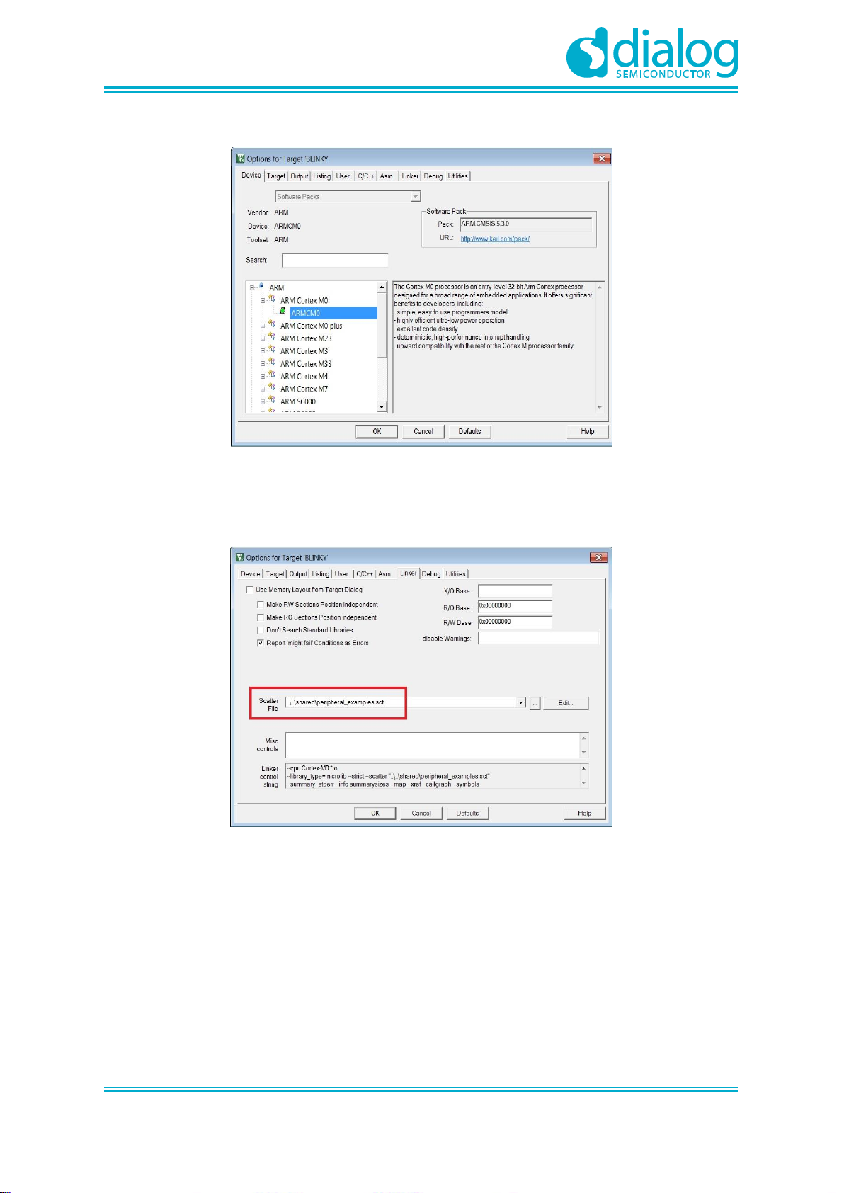
3. Click on the Target Options button, then click on the Device tab. The dialog should look like this.
Page 18
UM-B-048
DA14585/DA14586 Getting Started Guide with the Basic Development Kit
User Manual
Revision 2.0
09-Jul-2018
CFR0012-00 Rev 2
18 of 29
© 2018 Dialog Semiconductor
Figure 19: Blinky Project Options
4. Click on Linker. Scatter files (.sct) are used for selecting memory areas.
Figure 20: Blinky Project Scatter File
5. Click on Debug and ensure J-LINK/J-TRACE Cortex is selected and that the Initialization File
is set correctly to .sysram.ini.
Page 19

UM-B-048
DA14585/DA14586 Getting Started Guide with the Basic Development Kit
User Manual
Revision 2.0
09-Jul-2018
CFR0012-00 Rev 2
19 of 29
© 2018 Dialog Semiconductor
Figure 21: Blinky Project: Debug Option
6. Click on Settings and check that the SW Device has been detected correctly.
Figure 22: Blinky Project: Jlink setup
7. Click OK to save the settings in both windows. All settings have now been saved and you can
continue to build the example.
8. Build the project by pressing F7 key, or clicking the Build button, see Figure 23.
Page 20

UM-B-048
DA14585/DA14586 Getting Started Guide with the Basic Development Kit
User Manual
Revision 2.0
09-Jul-2018
CFR0012-00 Rev 2
20 of 29
© 2018 Dialog Semiconductor
Figure 23: Blinky Project: Project Building
9. Make sure you have a UART connection between your PC and the motherboard, as shown in
Figure 8. Check the COM number on your PC.
10. Open Tera Term, choose the COM port from step 9, and click OK.
11. Select Setup > Serial Port to configure the port as shown in Table 1.
12. In Keil, select Debug > Start/Stop Debug Session.
Figure 24: Blinky Project: Start Debug Session
13. If a non-licensed version of Keil is used, the following dialog is displayed. Click OK.
Figure 25: Keil Lite Pop Up Window
14. Press F5 or click the Run button to start code execution.
Page 21

UM-B-048
DA14585/DA14586 Getting Started Guide with the Basic Development Kit
User Manual
Revision 2.0
09-Jul-2018
CFR0012-00 Rev 2
21 of 29
© 2018 Dialog Semiconductor
Figure 26: Blinky Project: Code Execution
When the blinky message is displayed on your UART terminal screen and the green LED is blinking
you have successfully programmed and started the blinky program on DA14585/586 Demo board.
Figure 27: Blinky Project: Blinky message on COM28 terminal
9.2 The Barebone BLE Example Application
The Barebone BLE example application demonstrates basic BLE procedures such as advertising,
connection, updating connection parameters, and implementation of the Device Information Service
Server (DISS). See the Bluetooth SIG for more details.
1. Open the folder containing the SDK files. This is the folder where you extracted the SDK zip file.
2. In <sdk_root_directory>\projects\target_apps\ble_examples\ble_app_barebone\Keil_5, double-
click ble_app_barebone.uvproj to open the project in Keil.
Page 22

UM-B-048
DA14585/DA14586 Getting Started Guide with the Basic Development Kit
User Manual
Revision 2.0
09-Jul-2018
CFR0012-00 Rev 2
22 of 29
© 2018 Dialog Semiconductor
Figure 28: Barebone BLE Project directory
Figure 29 shows the Keil project layout.
Figure 29: Barebone BLE: KEIL Project Layout
3. To execute the code and run the example, repeat steps 3 to 14 in The Blinky Peripheral Example
Application.
The barebone application does not use the UART and so the only jumpers required are those for
the debugger interface as noted in Table 3.
4. Use the Android application BLE Scanner to scan for, and connect to, the DIALOG-BRBN app,
see Figure 30.
Page 23

UM-B-048
DA14585/DA14586 Getting Started Guide with the Basic Development Kit
User Manual
Revision 2.0
09-Jul-2018
CFR0012-00 Rev 2
23 of 29
© 2018 Dialog Semiconductor
Figure 30: Barebone BLE: Interacting with BLE Application
Your BLE application is now running and advertising using the default advertiser string: "DIALOGBRBN".
Note: In this example, we used an Android application but you can also use the LightBlue iOS
application to connect an iPad/iPod/iPhone device to the application.
Page 24

UM-B-048
DA14585/DA14586 Getting Started Guide with the Basic Development Kit
User Manual
Revision 2.0
09-Jul-2018
CFR0012-00 Rev 2
24 of 29
© 2018 Dialog Semiconductor
GPIO
Function
Jumper
P0_4
UART2 TX
Connect J4.11 - J4.12
P0_5
UART2 RX
Connect J4.13 - J4.14
P1_0
LED
Connect J9.1 – J9.2
JTAG
Function
Jumper
TMS
SWD IO
Connect J4.25 - J4.26
TCK
SWD CLK
Connect J4.27 - J4.28
9.3 Troubleshooting
• If you can't see any blinky messages in your UART terminal and the LED is not blinking, check
the UART and LED jumper configuration, see Table 2. You can also make sure that the hardware
configuration is set for, see Figure 31 in Appendix A
Table 2: Blinky Example UART and LED Jumper Configuration
If you can't start a debug session, check the SWD debugger jumper configuration, see Table 3.
Table 3: Blinky Example SWD Debugger Jumper Configuration
If you have trouble with the J-link firmware or any issue with SDK operation, refer to the DA1458x/68x
Development Kit J-Link Interface Application Note AN-B-052.
Note: If none of these actions resolved the issue, please contact Dialog Software Forum.
9.4 What Next ?
This tutorial does not cover all the topics relevant to software development environments, it describes
the first steps necessary to get started with the Pro Development Kit. The following links provide more
information on DA14585/586:
• DA14585 Product Brief: To know more about the SmartBond™ DA14585 SoC.
• DA14586 Product Brief: To know more about the SmartBond™ DA14586 SoC.
• UM-B-079: DA14585/586 SDK 6 Software Platform Reference: To know more about software
architecture.
• UM-B-080: DA14585/586 SDK 6 Software Developer’s Guide: To build more BLE and peripheral
examples.
• Codeless Tutorial: To quick start your IoT application and learn more about AT commands.
• Sleep mode configurations and power measurement: To learn more DA14585/586 Power
management.
• Application Hardware Design Guideline : To learn how to prepare schematics and PCB layouts
for your application.
Page 25

UM-B-048
DA14585/DA14586 Getting Started Guide with the Basic Development Kit
User Manual
Revision 2.0
09-Jul-2018
CFR0012-00 Rev 2
25 of 29
© 2018 Dialog Semiconductor
10 Appendices
10.1 Appendix A: Using the Basic Development Kit
The user_periph_setup.h file contains hardware settings related to the used. The default is the
ProDev Kit.
Figure 31: Hardware Settings for Basic Development Kit
10.2 Appendix B: Latency Timer of the FTDI cable
If an external FTDI cable is used to burn the OTP (or to download the image into the external memory),
the latency timer of the FTDI cable has to be changed from 15 ms to <10 ms.
To change the latency timer:
1. In the Windows Device Manager, expand the list of COM ports.
2. Right click on the required COM port and select Properties.
3. In the Port Settings tab, click Advanced.
4. Set the Latency Timer to < 10 ms.
Figure 32: FTDI Latency Timer
Page 26

UM-B-048
DA14585/DA14586 Getting Started Guide with the Basic Development Kit
User Manual
Revision 2.0
09-Jul-2018
CFR0012-00 Rev 2
26 of 29
© 2018 Dialog Semiconductor
10.3 Appendix C: Power Management: measuring current
The design of the DA14585 and DA14586 Basic Development Kit is made in such a way that the
microcontroller can be isolated completely from the rest of the board. This is illustrated in the block
diagram shown in Figure 33 and Figure 34 that showing the connections of the jumpers J4, J5 and
J6.
Figure 33: Setup of DA14585 Basic Development Kit during power measurement
Figure 34: Setup of DA14586 Basic Development Kit during power measurement
Page 27

UM-B-048
DA14585/DA14586 Getting Started Guide with the Basic Development Kit
User Manual
Revision 2.0
09-Jul-2018
CFR0012-00 Rev 2
27 of 29
© 2018 Dialog Semiconductor
Steps how to do the power measurements:
1. Connect the Current Meter to jumper J5.
2. Mount the jumpers needed for downloading the software.
3. Download the software.
4. Start the software.
5. Wait till software has reached ‘Deep Sleep’.
6. Dismount all the jumpers.
Now almost all the DA14585/586 pins are isolated and only the current meter and GND are connected.
7. Read the current.
For additional info: see AN-B-015 DA14580/581 Supply current measurements. See chapter 4.4 Deep
Sleep current measurement.
Page 28

UM-B-048
DA14585/DA14586 Getting Started Guide with the Basic Development Kit
User Manual
Revision 2.0
09-Jul-2018
CFR0012-00 Rev 2
28 of 29
© 2018 Dialog Semiconductor
Revision
Date
Description
1.0
27-Aug-2015
Initial version for DA1458x family with SDK 5.
1.1
20-Oct-2015
Minor Update in Keil installation instructions.
1.2
22-Jan-2017
Add DA14585/586.
2.0
09-Jul-2018
First HTML released version. Keep only DA14585/586.
Status
Definition
DRAFT
The content of this document is under review and subject to formal approval,
which may result in modifications or additions.
APPROVED or
unmarked
The content of this document has been approved for publication.
11 Revision history
Table 4: Revision history
12 Status definitions
Table 5: Status Definitions
13 Disclaimer
Information in this document is believed to be accurate and reliable. However, Dialog Semiconductor
does not give any representations or warranties, expressed or implied, as to the accuracy or
completeness of such information. Dialog Semiconductor furthermore takes no responsibility
whatsoever for the content in this document if provided by any information source outside of Dialog
Semiconductor.
Dialog Semiconductor reserves the right to change without notice the information published in this
document, including without limitation the specification and the design of the related semiconductor
products, software and applications.
Applications, software, and semiconductor products described in this document are for illustrative
purposes only. Dialog Semiconductor makes no representation or warranty that such applications,
software and semiconductor products will be suitable for the specified use without further testing or
modification. Unless otherwise agreed in writing, such testing or modification is the sole responsibility
of the customer and Dialog Semiconductor excludes all liability in this respect.
Customer notes that nothing in this document may be construed as a license for customer to use the
Dialog Semiconductor products, software and applications referred to in this document. Such license
must be separately sought by customer with Dialog Semiconductor.
All use of Dialog Semiconductor products, software and applications referred to in this document are
subject to Dialog Semiconductor’s Standard Terms and Conditions of Sale, unless otherwise stated.
Dialog and the Dialog logo are trademarks of Dialog Semiconductor plc or its subsidiaries. All other
product or service names are the property of their respective owners.
© 2018 Dialog Semiconductor. All rights reserved.
Page 29

UM-B-048
DA14585/DA14586 Getting Started Guide with the Basic Development Kit
User Manual
Revision 2.0
09-Jul-2018
CFR0012-00 Rev 2
29 of 29
© 2018 Dialog Semiconductor
Contacting Dialog
Semiconductor
name
contacting-dialogsemiconductor
:class: ContactHeading
United Kingdom
(Headquarters)
Dialog Semiconductor
PLC
Phone: +44 1793 757700
Germany
Dialog Semiconductor
GmbH
Phone: +49 7021 805-0
The Netherlands
Dialog Semiconductor
B.V.
Phone: +31 73 640 8822
North America
Dialog Semiconductor
Inc.
Phone: +1 408 845
8500
Japan
Dialog Semiconductor
K. K.
Phone: +81 3 5769
5100
Taiwan
Dialog Semiconductor
Taiwan
Phone: +886 281 786
222
Hong Kong
Dialog
Semiconductor Hong
Kong
Phone: +852 2607
4271
Korea
Dialog
Semiconductor
Korea
Phone: +82 2 3469
8200
China (Shenzen)
Dialog
Semiconductor
China
Phone: +86 755
2981 3669
China (Shanghai)
Dialog
Semiconductor
China
Phone: +86 21
5424 9058
Email:
enquiry@diasemi.com
Web site:
https://www.dialogsemiconducto
r.com/
Table 6: Dialog Semiconductor
14 RoHS Compliance
Dialog Semiconductor complies to European Directive 2001/95/EC and from 2 January 2013 onwards
to European Directive 2011/65/EU concerning Restriction of Hazardous Substances (RoHS/RoHS2).
Dialog Semiconductor’s statement on RoHS can be found on the DA1458x RoHS 2 declaration. RoHS
certificates from our suppliers are available on request.
 Loading...