

ANZALPHA
2A
Product description:
-Module Guideline Bluetooth module operating manual
2AANZ
and efficient mono wireless transmission solution. It’s adopt domestic Jieli Bluetooth chip AC6925B.
It’s provides the module with high quality sound and compatibility, and overall performance more
optimized.
2AANZ
module to the application products, connect with power, then it can achieve the wireless music
transfer, enjoy the funny of wireless music.
Application fields:
This module is used for short distance music transfer, is easy to connect with smart computer,
phone, PDA etc. Products’ Bluetooth device, to gain the wireless music transfer.
※ Bluetooth speaker
※ Bluetooth headphone
※ Hands-free calls
※ Wireless transfer audio.
ALPHA
ALPHA
-Module Bluetooth module is smart wireless audio data input product, is a low cost
-Module Bluetooth module is using for driveless mode. You only need input the
Product Specification:
Item No.
Bluetooth version Bluetooth V5.0+EDR
Support bluetooth
agreement:
Working Ampere
Standby Voltage < 300uA
Working Voltage 3.3V-5.5V
Temperature Range
Wireless Range
T r a n s m i t P o w e r Class2 Max 4dB
2AANZ
AVRCP 1.0,GAVDP 1.0,AVDTP 1.0,A2DP 1.2,
Hands-Free Profile 1.5,Headset Profile v1.1
≤30mA
-40ºC to +80ºC
>10 M
ALPHA
-Module

Sensitivity -80dBm@0.1%BER
Frequency Range 2.402GHz-2.480GHz
External interface
PIO,UART
Audio Performance High quality music
Audio signal to noise ratio
Distortion
≥75dB
≤0.1%
Module size 46.00X35.00X1.00mm
Product Size drawing:

:
Warning:
This device complies with Part 15 of the FCC Rules. Operation is subject to the following two
conditions : (1) this device may not cause harmful interference, and (2) this device must accept any
interference received, including interference that may cause undesired operation.
Warning: Changes or modifications to this unit not expressly approved by the party responsible for
compliance could void the user’s authority to operate the equipment.
NOTE: This equipment has been tested and found to comply with the limits for a Class B digital
device, pursuant to Part 15 of the FCC Rules. These limits are designed to provide reasonable
protection against harmful interference in a residential installation. This equipment generates, uses
and can radiate radio frequency energy and, if not installed and used in accordance with the
instructions, may cause harmful interference to radio communications.
However, there is no guarantee that interference will not occur in a particular installation. If this
equipment does cause harmful interference to radio or television reception, which can be determined
by turning the equipment off and on, the user is encouraged to try to correct the interference by one
or more of the following measures:
Reorient or relocate the receiving antenna.
Increase the separation between the equipment and receiver.
Connect the equipment into an outlet on a circuit different from that to which
the receiver is connected.
Consult the dealer or an experienced radio/TV technician for help
This device complies with Part 15, Part 15.247 of the FCC Rules. The FCC ID for this device is
2AANZ
If the FCC ID is not visible with the module is installed inside another device,then it must be still
responsible for the FCC compliance requirement of the end product which referring to the enclosed
module and it also must display a label, such as the following:
Contains Transmitter module FCC ID:
The Module can be installed in Portable device only, and it can not be installed in any Mobile Device.
The host product manufacturer is responsible for compliance to any other FCC rules that apply to the host
not covered by the m odular transmitter grant of certification. The final host product still requires Part 15
Subpart B compliance testing with the modular transmitter installed. The end user manual shall include all
required regulatory information / warning as shown in this manual, include: The portable has been
evaluated to meet general RF exposure requirement. The device can be used in portable exposure
condition without restriction.
ALPHA
.
2AANZ
ALPHA
or contains FCC ID:
2AANZ
ALPHA

Antenna Specification
Summary
ITEM ANT SPEC
Model Name 2.4G ANT
Horizontal Vertical
Center
Frequency
MAX. Gain -0.58dB
Polarization Horizontal and Vertical
Azimuth Beam
Pattern
Impedance 50 Ohm
Antenna Length 38.20mm
Manufacture ZHUHAI JIELI TECHNOLOGY CO.,LTD
2400MHz 2400MHz 2500MHz 2400MHz 2400MHz 2500MHz
-1.26 -0.76 -0.58 -5.25 -2.46 -1.86
Omni-directional
Antenna Photo & Length (mm)

Horizontal:
Power (dBm)
2400 MHz 2450 MHz 2500 MHz
Max: 0 Min: -40 Scale: 5/div
Gain(dB) Frequency
(MHz)
2400 -1.26174 -30.0801 -7.18716
2450 -0.765802 -36.5604 -7.48023
2500 -0.585582 -22.0315 -6.59127
Max Min Avg

Vertical:
2400 MHz 2450 MHz 2500 MHz
Power (dBm)
Max: 0 Min: -30 Scale: 5/div
Gain(dB) Frequency
(MHz)
2400 -5.2537 -22.1424 -12.4294
2450 -2.4652 -24.5837 -10.4702
2500 -1.86120 -29.5214 -9.20432
Max Min Avg
ANT Test Labs:Attestation of Global Compliance Co., Ltd.

Hardware Design Guidance
Power supply、ground wire
1、 Ground wire
The bluetooth ground wire are divided into AGND、PGND、and GND:
a)
AGND and GND must be strictly distinguished, connected at the battery entrance or in the front of IC
ground side; in the case of limited PCB board space, priority should be given to ensuring the connectivity of
GND and the battery ground circuit, and the route must be thick .
b) PGND and GND must be strictly distinguished,PGND go back to chip side behind of base pin and connect
GND nearby.
2、DCDC Picture 1. DC-DC switching power circuit
DC-DC
Like picture 1,
red color);L2/C3/C4/C9 should be as close as possible to the base pin in layout;C3/C4/C9 ground circuit must return
to the PGND pin at the shortest distance (no holes and as thick as possible), L2 + 1.5V routing must first pass the C4
(106) capacitort then go into IC (refer to picture 2);L2 should be as far away from the easily disturbed parts (such as
RF and DAC) as possible;. Do not install any signal line under the inductor or L2 should choose winding inductor or
power laminated inductor with minimum impedance
switching power circuit is composed ofSW、
Picture 2. Ground Circuit of DC-DC Switching Power Supply
PGND
、BT_
AVDD、
L2、C3、C4、C9 (marked

+1.5V power supply should as thick as possible and ,routing should first pass the capacitor then go into IC,it
is not allow to through the hole connect IC after passing capacitor .
3、LDOIN
LDOIN decoupling capacitor C5 is placed as close as possible to the pin of the chip and connected to PGND,
same time LDOIN should be as thick as possible, routing should first pass the capacitor then go into IC
4、VDDIO
The decoupling capacitor C6 of VDDIO should place as close as possible to the chip 2 pin side.
Signal line
1、Crystal oscillator Picture 3.
a) CrystaloscillatorY1shouldplace ascloseaspossibletothechippin,capacitor C23、C24 centralizedlayout(avoidC23、C24atthe
eachsideof crystaloscillator),andfindtheshortestwaytothechippin2(VSSIO);
b)IncaseofPCBsizeislimited,C24isallowedtobeplacednearthechipandmakesureitistheshortestdistancebacktochippin
2(VSSIO).
c)
CrystaloscillatorY1 requires good stability and consistency,frequency deviation within (±
10PPM);the siz e of loading capacitor C23 and C24 de pend on the size of crystal oscillator loading
capacitor,be subjected to actual testing(recommend use JL matched crystal oscillator).
2、RF antenna Picture 4. Antenna layout

a)RFtry place at the PCB side, can not have metal components on both front and back sides, use three side hollow-out way (top,left and right like picture 4).
Picture5.
b)RF and DAC circuit must in 1800layout to minimize the interference from RF to DAC .
c)If PCB have enough space be sure to use inverted F-shaped antenna.
d)Try to place RF like I -shaped.
3、DAC、MIC、VCOM、DACVDD
a)
DAC circuits and solder joints must be placed 180 degrees with RF to reduce the radiation and
interference from RF.
b) DAC circuits and solder joints ,AGND on the back or not, must not place under the DC-DC power
GND,otherwise there will be high- frequency noise, refer to picture 6.
Picture6. Wrong Layout and Routing of DAC Circuit Placed under DC-DC Power Circuit
c)MIC circuits and solder joints ,VCOM and DACVDD decoupling capacitors,withorwithoutAGND,otherwise
easilybeinterferedbyRFandmakehighfrequencynoise.
d) Do not lay “digital GND” under the three signal lines DACL、DACR and VCOMO ,aswellas anti-
interferencecapacitorsand inductors, stay awayfrom“digitalGND”.

Additions
Picture7. DAC restrain RF interference circuit
1、RF antenna、TDD radiation noise
a)Picture7 is the circuit of DAC retrain RF antenna and TDD interference,itisrecommendedtoreserve,ifhas
limitedspacethencanjustreserveR6/R7/R8.
b)DAC、power supply lead and speaker cavity should avoid the RF position, the back of RF is the best position
for speaker and battery connection point.(Note: the noise disposing circuit of DAC will increase cost,if
solution design is reasonable enough and not highly require noise it can not be reserved.
2、ESD disposing
Picture8. ESD static electricity disposing circuit
a) Likepicture8nearthechipDACVDD pin,AGND of C1 decoupling capacitor tandem connect capacitor
105 to GND nearby.
b) Likepicture8nearthechipRTCVDD pin ,RTCVDD tandem connect magnetic bead L1 ,then tandem
connectGNDof capacitor C3.(Note: ESD dispose willincrease material, it cannot be considered if solution
have no this requirement.)

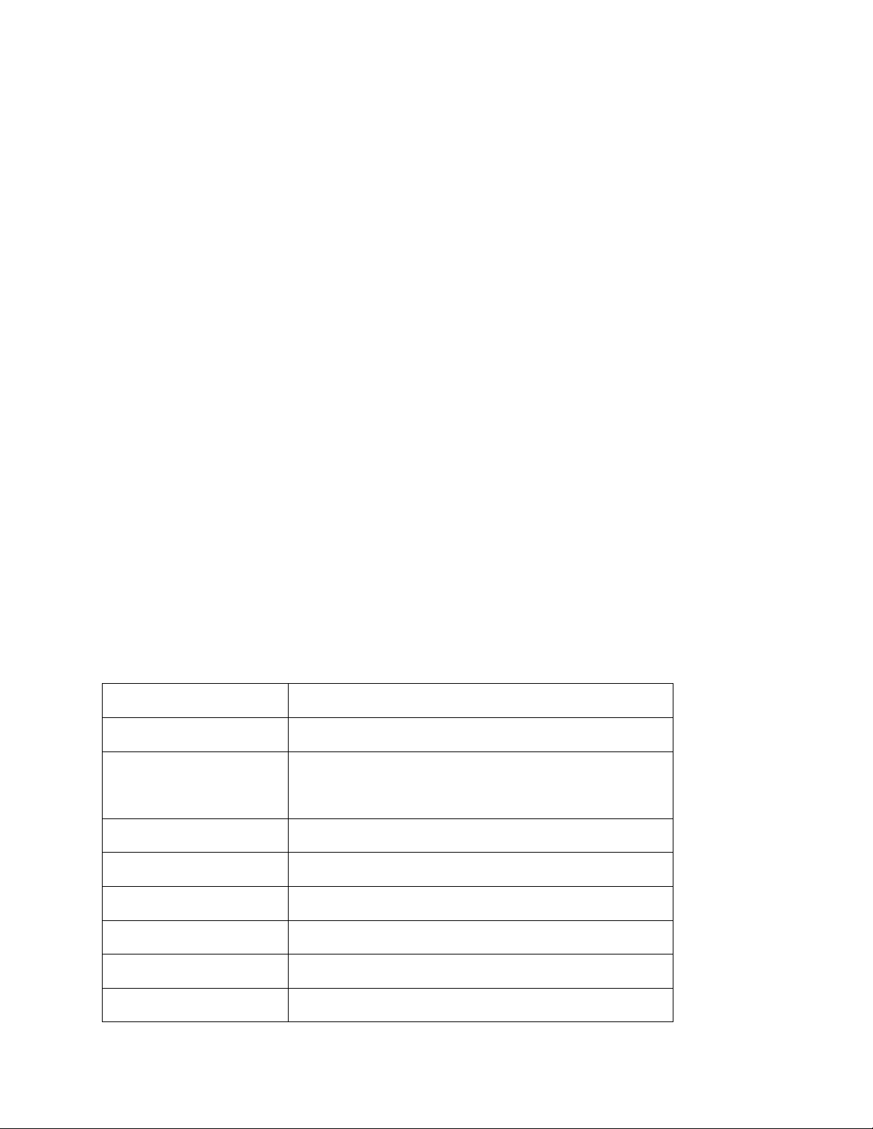
Version information
Date Version
No.
2016.03.30 V1.0
2016.04.28 V1.1
2016.05.18 V1.2
Description
Original version
1、 increased +1.5V power supply description
2、increasedLDOIN power supply description
3、 increased crystal oscillatordescription( point b )
4、 increased RF layout description(point d )
5、 increased DAC description(point c and d )
1、 increased ground description.
2、 the decoupling capacitor of LDOIN connect PGND.
3、 updated picture 1 and 2.
 Loading...