

Page 1
www.d.comChapter 1 Introduction
1
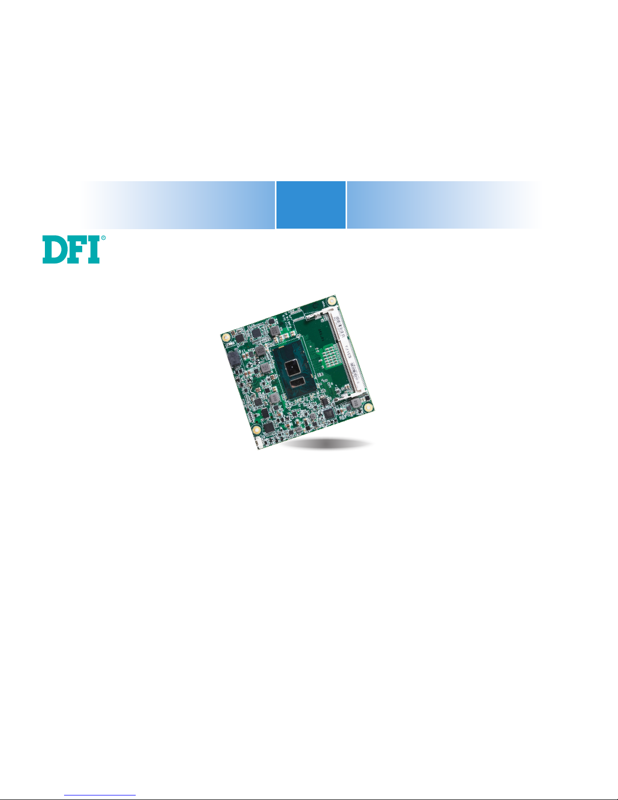
SU968
COM Express Compact Module
User’s Manual
A41300702
Page 2

www.d.comChapter 1 Introduction
2
Copyright
This publication contains information that is protected by copyright. No part of it may be reproduced in any form or by any means or used to make any transformation/adaptation without
the prior written permission from the copyright holders.
This publication is provided for informational purposes only. The manufacturer makes no
representations or warranties with respect to the contents or use of this manual and specifically disclaims any express or implied warranties of merchantability or fitness for any particular
purpose. The user will assume the entire risk of the use or the results of the use of this document. Further, the manufacturer reserves the right to revise this publication and make changes
to its contents at any time, without obligation to notify any person or entity of such revisions
or changes.
Changes after the publication’s first release will be based on the product’s revision. The website
will always provide the most updated information.
© 2017. All Rights Reserved.
Trademarks
Product names or trademarks appearing in this manual are for identification purpose only and
are the properties of the respective owners.
COM Express Specification Reference
PICMG® COM Express ModuleTM Base Specification.
http://www.picmg.org/
FCC and DOC Statement on Class B
This equipment has been tested and found to comply with the limits for a Class B digital
device, pursuant to Part 15 of the FCC rules. These limits are designed to provide reasonable protection against harmful interference when the equipment is operated in a residential
installation. This equipment generates, uses and can radiate radio frequency energy and, if not
installed and used in accordance with the instruction manual, may cause harmful interference
to radio communications. However, there is no guarantee that interference will not occur in a
particular installation. If this equipment does cause harmful interference to radio or television
reception, which can be determined by turning the equipment off and on, the user is encouraged to try to correct the interference by one or more of the following measures:
• Reorient or relocate the receiving antenna.
• Increase the separation between the equipment and the receiver.
• Connect the equipment into an outlet on a circuit different from that to which the receiver
is connected.
• Consult the dealer or an experienced radio TV technician for help.
Notice:
1. The changes or modifications not expressly approved by the party responsible for compliance could void the user’s authority to operate the equipment.
2. Shielded interface cables must be used in order to comply with the emission limits.
Page 3

www.d.comChapter 1 Introduction
3
Chapter 1 - Introduction............................6
Specifications ...........................................................................6
Features .................................................................................7
Chapter 2 - Concept..................................8
COM Express Module Standards................................................8
Specification Comparison Table .................................................9
Chapter 3 - Hardware Installation ............ 10
Board Layout .........................................................................10
Block Diagram .......................................................................10
Mechanical Diagram ...............................................................11
System Memory .....................................................................12
Connectors ............................................................................ 13
CPU Fan Connector ................................................................... 13
COM Express Connectors .......................................................... 13
COM Express Connectors .......................................................... 14
COM Express Connectors Signals and Descriptions ....................... 15
Standby Power LED ...............................................................22
Cooling Option ....................................................................... 22
Installing SU968 onto a Carrier Board ..................................... 23
Installing the COM Express Debug Card ..................................25
Chapter 4 - BIOS Setup .......................... 27
Overview .............................................................................. 27
Insyde BIOS Setup Utility .......................................................28
Main ....................................................................................... 28
Advanced ............................................................................... 28
Security .................................................................................. 35
Boot ....................................................................................... 36
Exit ........................................................................................ 38
Updating the BIOS ................................................................. 39
Notice: BIOS SPI ROM ........................................................... 39
Chapter 5 - Supported Software .............. 41
Chapter 6 - RAID ................................... 55
Chapter 7 - Intel AMT Settings ............... 59
Appendix A - Troubleshooting .................. 72
Table of Contents
Appendix B - Insyde BIOS Standard Status POST Code
........................................................................74
Page 4
www.d.comChapter 1 Introduction
4
About this Manual
An electronic file of this manual is included in the DVD. To view the user’s manual in the DVD,
insert the DVD into a DVD-ROM drive. The autorun screen (Main Board Utility DVD) will appear. Click “User’s Manual” on the main menu.
Warranty
1. Warranty does not cover damages or failures that arised from misuse of the product,
inability to use the product, unauthorized replacement or alteration of components and
product specifications.
2. The warranty is void if the product has been subjected to physical abuse, improper installation, modification, accidents or unauthorized repair of the product.
3. Unless otherwise instructed in this user’s manual, the user may not, under any circumstances, attempt to perform service, adjustments or repairs on the product, whether in or
out of warranty. It must be returned to the purchase point, factory or authorized service
agency for all such work.
4. We will not be liable for any indirect, special, incidental or consequencial damages to the
product that has been modified or altered.
Static Electricity Precautions
It is quite easy to inadvertently damage your PC, system board, components or devices even
before installing them in your system unit. Static electrical discharge can damage computer
components without causing any signs of physical damage. You must take extra care in handling them to ensure against electrostatic build-up.
1. To prevent electrostatic build-up, leave the system board in its anti-static bag until you are
ready to install it.
2. Wear an antistatic wrist strap.
3. Do all preparation work on a static-free surface.
4. Hold the device only by its edges. Be careful not to touch any of the components, contacts
or connections.
5. Avoid touching the pins or contacts on all modules and connectors. Hold modules or connectors by their ends.
Safety Measures
To avoid damage to the system:
• Use the correct AC input voltage range.
To reduce the risk of electric shock:
• Unplug the power cord before removing the system chassis cover for installation or servicing. After installation or servicing, cover the system chassis before plugging the power
cord.
Important:
Electrostatic discharge (ESD) can damage your processor, disk drive and other components. Perform the upgrade instruction procedures described at an ESD workstation only. If such a station is not available, you can provide some ESD protection by
wearing an antistatic wrist strap and attaching it to a metal part of the system chassis. If a wrist strap is unavailable, establish and maintain contact with the system
chassis throughout any procedures requiring ESD protection.
Page 5

www.d.comChapter 1 Introduction
5
About the Package
The package contains the following items. If any of these items are missing or damaged,
please contact your dealer or sales representative for assistance.
• One SU968 board
• One DVD
• One Heat Sink (Height: 23.8mm)
Optional Items
• COM332-B Carrier Board Kit
• Heat spreader (Height: 11mm)
The board and accessories in the package may not come similar to the information listed
above. This may differ in accordance with the sales region or models in which it was sold. For
more information about the standard package in your region, please contact your dealer or
sales representative.
Before Using the System Board
Before using the system board, prepare basic system components.
If you are installing the system board in a new system, you will need at least the following
internal components.
• Storage devices such as hard disk drive, CD-ROM, etc.
You will also need external system peripherals you intend to use which will normally include at
least a keyboard, a mouse and a video display monitor.
Page 6
www.d.comChapter 1 Introduction
6
WatchDog
Timer
Output &
Interval
System Reset, Programmable via Software from 1 to 255 Seconds
Security TPM Available Upon Request
Power Type 12V, 5VSB, VCC_RTC (ATX mode)
12V, VCC_RTC (AT mode)
Consumption Typical: I7-6600U: 12V @ 0.86A (10.28Watt)
Max.: I7-6600U: 12V @ 1.372A (16.46Watt)
OS Support Windows 7 (/WES7) 32/64-bit
Windows 8.1 (64-bit)
Windows 10 IoT Enterprise 64-bit
Debian 8 (with VESA graphic driver)
CentOS 7 (with VESA graphic driver)
Ubuntu 15.10 (Intel graphic driver available)
Environment Temperature Operating
: 0 to 60°C
: -45 to 80°C -40 to 85°C (with heat spreader)
Storage: -40 to 85°C
Humidity Operating: 5 to 90% RH
Storage: 5 to 90% RH
MTBF 921,923 hrs @ 25°C; 460,715 hrs @ 45°C; 256,677 hrs @ 60°C
Calculation Model: Telcordia Issue 2, Method Case 3
Environment: GB, GC – Ground Benign, Controlled
Mechanical Dimensions COM Express® Compact
95mm (3.74") x 95mm (3.74")
Compliance PICMG COM Express® R2.1, Type 6
Chapter 1 - Introduction
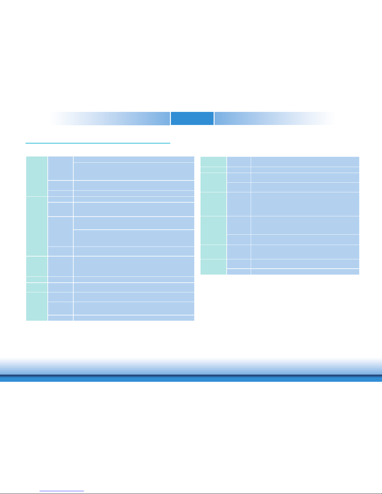
Specifications
Chapter 1
System Processor 6th Generation Intel® CoreTM Processors, BGA 1 356
Intel® CoreTM i7-6600U Processor, Dual Core, 4M Cache, 2.6GHz (3.4GHz), 15W
Intel® CoreTM i5-6300U Processor, Dual Core, 3M Cache, 2.4GHz (3.0GHz), 15W
Intel® CoreTM i3-6100U Processor, Dual Core, 3M Cache, 2.3GHz, 15W
Intel® Celeron® Processor 3955U, Dual Core, 2M Cache, 2.0GHz, 15W
Memory Two 204-pin SODIMM up to 16GB
Dual Channel DDR3L 1600MHz
BIOS Insyde SPI 128Mbit
Graphics Controller Intel® HD Graphics GT Series
Feature OpenGL 5.0, DirectX 12, OpenCL 2.1
HW Decode:
AVC/H.264, MPEG2, VC1/WMV9, JPEG/MJPEG, HEVC/H265, VP8, VP9
HW Encode: AVC/H.264, MPEG2, JPEG, HEVC/H265, VP8, VP9
Display 1 x VGA/DD I (DDI available upon request)
1 x LVDS/ eDP (eDP available upon request)
1 x DDI
VGA: resolution up to 2560x1600 @ 60Hz
LVDS: dual channel 24-bit, resolution up to 1920x1200 @ 60Hz
HDMI: resolution up to 4096x2160 @ 24Hz or 2560x1600 @ 60Hz
DP++: resolution up to 4096x2304 @ 60Hz
Triple Displays VGA + LVDS + DDI
DDI + eDP + DDI
Expansion Interface 5 PCIe x1 or 4 PCIe x1 + 1 PCIe x4 or 3 PCIe x1 + 2 PCIe x2
1 x LPC
1 x I2C
1 x SMBus
2 x UART (TX/RX)
Audio Interface HD Audio
Ethernet Controller 1 x Intel® I219LM with iAMT11.0 PCIe (10/100/1000Mbps)
(only Core i7/i5 supports iAMT)
I/O USB 4 x USB 3.0
8 x USB 2.0
SATA 3 x SATA 3.0 (up to 6Gb/s) (Core i7/i5)
2 x SATA 3.0 (up to 6Gb/s) (Celeron)
RAID 0/1/5/10 (Core i7/i5 )
DIO 1 x 8-bit DIO
Page 7

www.d.comChapter 1 Introduction
7
Chapter 1
Features
• Watchdog Timer
The Watchdog Timer function allows your application to regularly “clear” the system at the set
time interval. If the system hangs or fails to function, it will reset at the set time interval so
that your system will continue to operate.
• DDR3L
DDR3L SDRAM provides backward compatibility to DDR3 memory modules but can operate at
the same or at a lower power level.
• Graphics
The integrated Intel® HD graphics engine delivers an excellent blend of graphics performance
and features to meet business needs. It provides excellent video and 3D graphics with outstanding graphics responsiveness. These enhancements deliver the performance and compatibility needed for today’s and tomorrow’s business applications. It supports VGA/DDI, LVDS/
eDP and DDI interfaces for 3 display outputs.
• Serial ATA
Serial ATA is a storage interface that is compliant with SATA 1.0a specification. With speed of
up to 6Gb/s (SATA 3.0), it improves hard drive performance to be faster than the standard
parallel ATA, which only has data transfer rate of 100MB/s. The bandwidth of the SATA 3.0 will
be limited by carrier board design.
• Gigabit LAN
The Intel® I219LM with iAMT11.0 Gigabit LAN controller supports up to 1Gbps data transmission (only Core i7/i5 supports iAMT).
• USB
The system board supports the new USB 3.0. It is capable of running at a maximum transmission speed of up to 5 Gbit/s (625 MB/s) and is faster than USB 2.0 (480 Mbit/s, or 60 MB/s)
and USB 1.1 (12Mb/s). USB 3.0 reduces the time required for data transmission, reduces
power consumption, and is backward compatible with USB 2.0. It is a marked improvement
in device transfer speeds between your computer and a wide range of simultaneously
accessible external Plug and Play peripherals.
Page 8
www.d.comChapter 2 Concept
8
Chapter 2
Chapter 2 - Concept
106.00
91.00
70.00
51.00
4.00
18.00
6.00
0.00
16.50
4.00
0.00
Extended
BasicCompact
Mini
74.20
80.00
91.00
121.00
151.00
Common for all Form Factors
Extended only
Basic only
Compact only
Compact and Basic only
Mini only
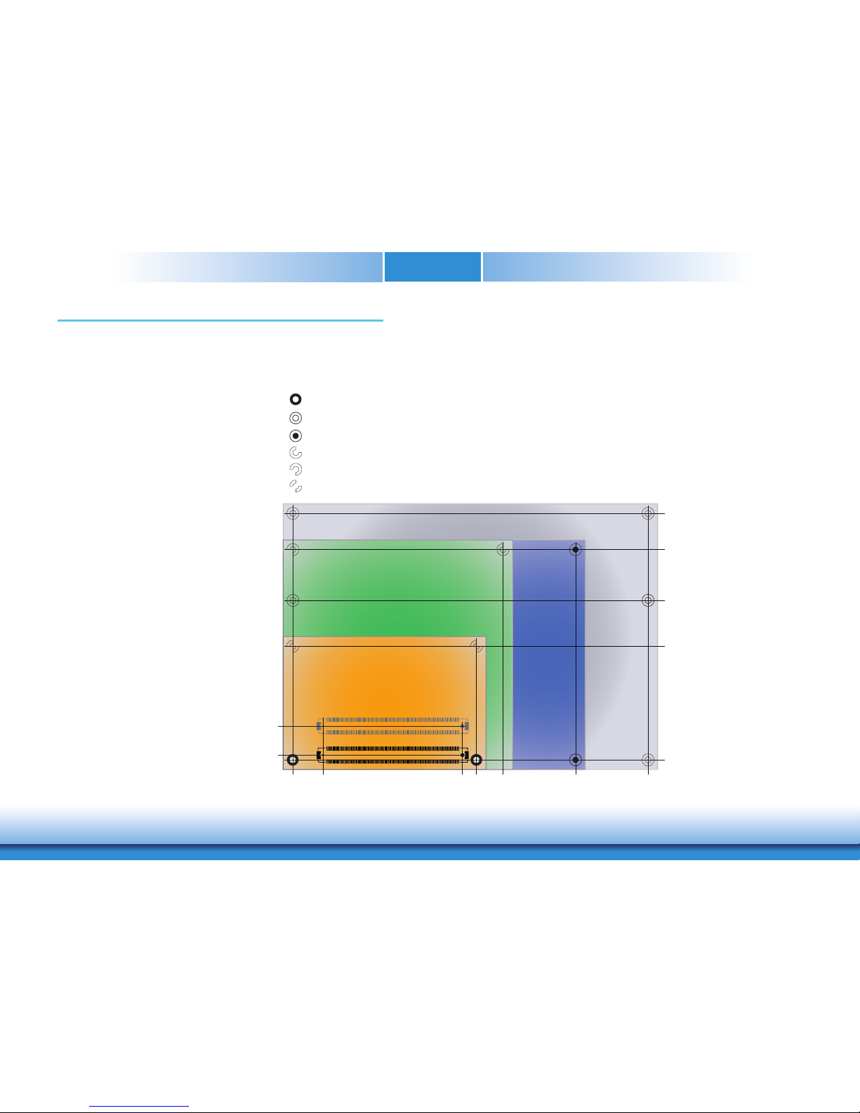
COM Express Module Standards
The figure below shows the dimensions of the different types of COM Express modules.
SU968 is a COM Express Compact module. The dimension is 95mm x 95mm.
Page 9
www.d.comChapter 2 Concept
9
Chapter 2
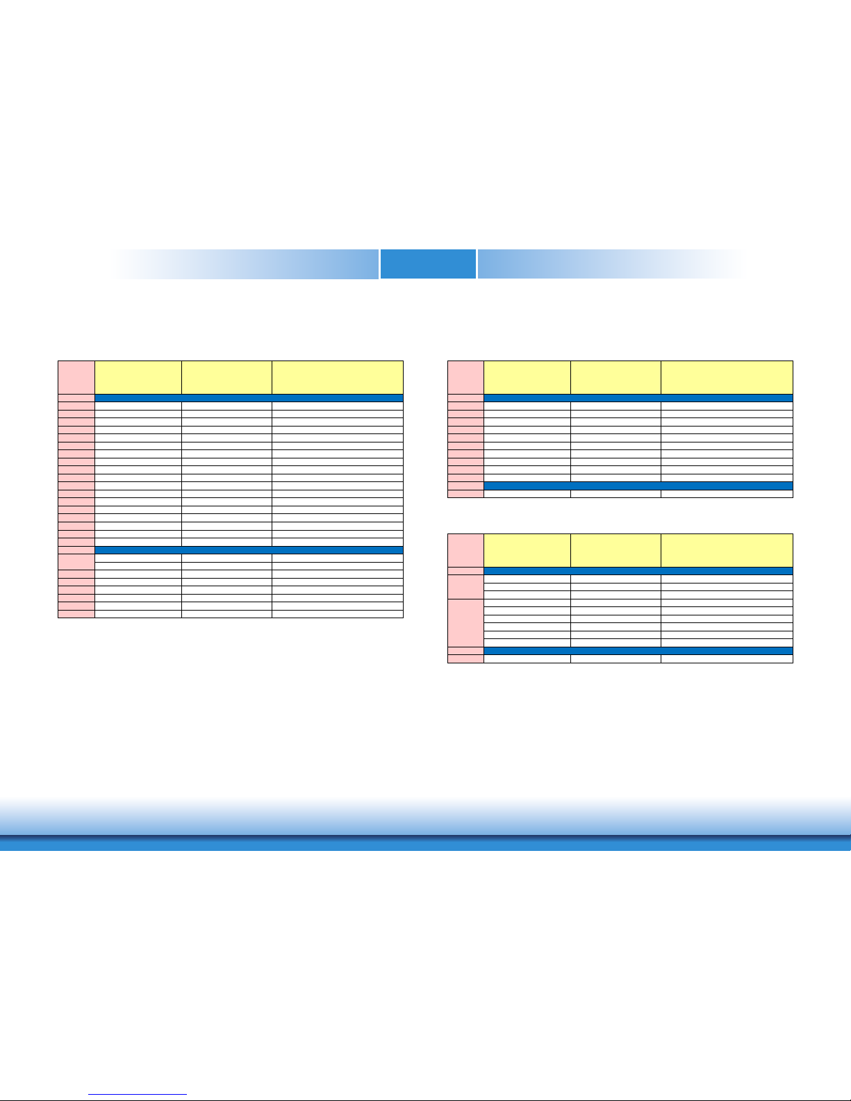
Specification Comparison Table
Module Pin-out - Required and Optional Features C-D Connector. PICMG® COM.0 Revision 2.1
The table below shows the COM Express standard specifications and the corresponding specifications supported on the SU968 module.
• 5 Indicates 12V-tolerant features on former VCC_12V signals.
• 6 Cells in the connected columns spanning rows provide a rough approximation of features
sharing connector pins.
Connector Feature
COM Express Module Base
Specification Type 6
(No IDE or PCI, add DDI+ USB3)
Min / Max
DFI SU968
Type 6
A-B
A-B
PCI Express Lanes 0 - 5 1 / 6 6
A-B LVDS Channel A 0 / 1 1
A-B LVDS Channel B 0 / 1 1
A-B eDP on LVDS CH A pins 0 / 1 1
A-B VGA Port 0 / 1 0/1 (Option : DDI2 or VGA)
A-B TV-Out NA NA
A-B DDI 0 NA NA
A-B
5
Serial Ports 1 - 2 0 / 2 2
A-B CAN interface on SER1 0 / 1 0
A-B SATA / SAS Ports 1 / 4
3 (with Intel® Celeron®: 2)
A-B AC’97 / HDA Digital Interface 0 / 1 1
A-B USB 2.0 Ports 4 / 8 8
A-B USB Client 0 / 1 0
A-B USB 3.0 Ports NA NA
A-B LAN Port 0 1 / 1 1
A-B Express Card Support 1 / 2 2
A-B LPC Bus 1 / 1 1
A-B SPI 1 / 2 1
A-B
SDIO (muxed on GPIO) 0 / 1 0
General Purpose I/O 8 / 8 8
A-B SMBus 1 / 1 1
A-B I2C 1 / 1 1
A-B Watchdog Timer 0 / 1 1
A-B Speaker Out 1 / 1 1
A-B External BIOS ROM Support 0 / 2 1
A-B Reset Functions 1 / 1 1
A-B
6
System I/O
System Management
Connector Feature
COM Express Module Base
Specification Type 6
(No IDE or PCI, add DDI+ USB3)
Min
/
Max
DFI SU968
Type 6
A-B
A-B Thermal Protection 0 / 1
1
A-B Battery Low Alarm 0 / 1
1
A-B Suspend/Wake Signals 0 / 3
1
A-B Power Button Support 1 / 1
1
A-B Power Good 1 / 1
1
A-B VCC_5V_SBY Contacts 4 / 4
4
A-B
5
Sleep Input 0 / 1
1
A-B
5
Lid Input 0 / 1
1
A-B
5
Fan Control Signals 0 / 2
2
A-B Trusted Platform Modules 0 / 1
1
A-B
A-B VCC_12V Contacts 12 / 12
12
Power
Power Management
Connector Feature
COM Express Module Base
Specification Type 6
(No IDE or PCI, add DDI+ USB3)
Min / Max
DFI SU968
Type 6
C-D
PCI Express Lanes 16 - 31
0 / 16
0
PCI Express Graphics (PEG) 0 / 1
0
Muxed SDVO Channels 1 - 2 NA
NA
PCI Express Lanes 6 - 15 0 / 2
2
PCI Bus - 32 Bit NA
NA
PATA Port NA
NA
LAN Ports 1 - 2 NA
NA
DDIs 1 - 3 0 / 3 1/2 (Option : DDI2 or VGA)
USB 3.0 Ports 0 / 4
4
C-D
C-D VCC_12V Contacts 12 / 12
12
System I/O
Power
C-D
6
C-D
6
Page 10
www.d.comChapter 3 Hardware Installation
10
Chapter 3
Chapter 3 - Hardware Installation
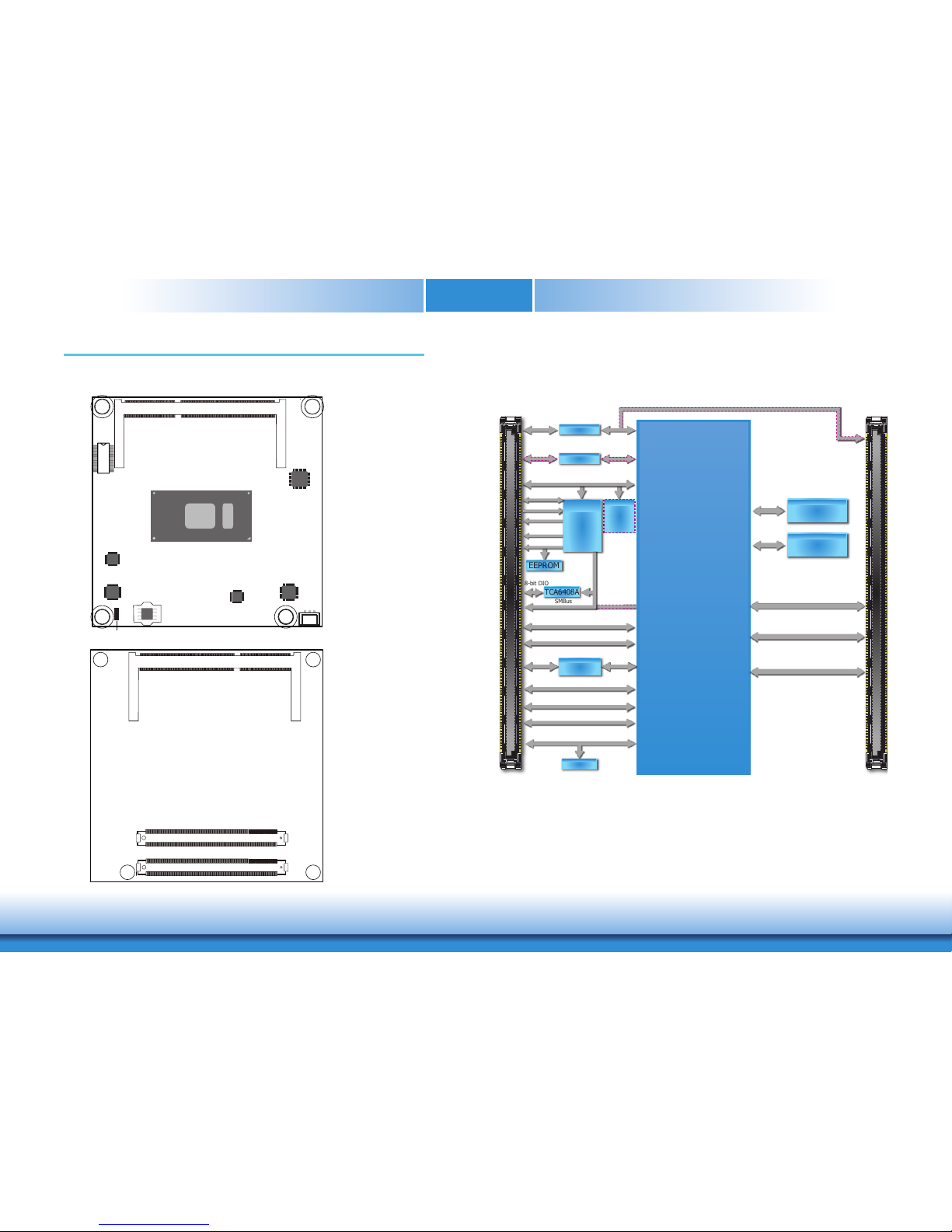
Board Layout
Top View
Bottom View
Block Diagram
EEPROM
SATA 3.0 3x
USB 3.0 4x
A / B
SMBus
6th Generation
Intel
®
Core™ i7/i5/i3
Intel® GLAN
I219LM
MDI
SPI Flash
SPI Bus
C / D
DDR3L 1600MHz
SODIMM
Channel A
PCIe x1
PCIe x1 (4 x1/2 x2/1 x4)
LPC Bus
8-bit DIO
WDT
I
2
C Bus
TPM
1.2/2.0
(optional)
Serial Port 0,1
Fan PWM/
TACH_IN
SLP/LID
TCA6408A
Embedded
Controller
IT8528E
DDI Port 1
HDA
USB 2.0 8x
eDP/DDI
(optional)
PTN3460
LVDS
(optional)
DDI
(optional)
CH7517
VGA
DDI Port 2
PCIe x1 (2 x1/1 x2)
PCIe x1 (2 x1)
DDR3L 1600MHz
SODIMM
Channel B
CPU Fan
1
SPI Flash BIOS
Intel
I219LM
Intel
BGA 1356
DDR3L_1 SODIMM
iTE
IT8528VG
PWMIC
NXP
PTN3460
Chrontel
CH7517
TPM (optional)
COM Express connector
C1
D1
C110
D110
B1
B110
A1
A110
COM Express connector
DDR3L_2 SODIMM
Page 11

www.d.comChapter 3 Hardware Installation
11
Chapter 3
Mechanical Diagram
Heat Sink
SU968 Module
20.3
1.5
+0.1
-0
3.5ā0.05
1.5
95
95
17
7
3
R3
Top View
Bottom View
0
4
16.50
45.28
809195
0
4
6
18
46.64
91
95
-+
208
0
4
6
18
91
95
0
4
16.50
80
95
1
71
73
DIMM2
Page 12

www.d.comChapter 3 Hardware Installation
12
Chapter 3
System Memory
Standby
Power LED
The system board is equipped with two 204-pin SODIMM sockets supporting up to 16GB
system memory and dual channel DDR3L 1600MHz memory interface.
DDR3L_1
SODIMM
Important:
Electrostatic discharge (ESD) can damage your board, processor, disk drives, add-in
boards, and other components. Perform installation procedures at an ESD workstation
only. If such a station is not available, you can provide some ESD protection by wearing an antistatic wrist strap and attaching it to a metal part of the system chassis. If
a wrist strap is unavailable, establish and maintain contact with the system chassis
throughout any procedures requiring ESD protection.
Important:
When the Standby Power LED is red, it indicates that there is power on the board.
Power-off the PC then unplug the power cord prior to installing any devices. Failure to
do so will cause severe damage to the board and components.
System Memory
Top View
Bottom View
DDR3L_2
SODIMM
Page 13
www.d.comChapter 3 Hardware Installation
13
Chapter 3
Connectors
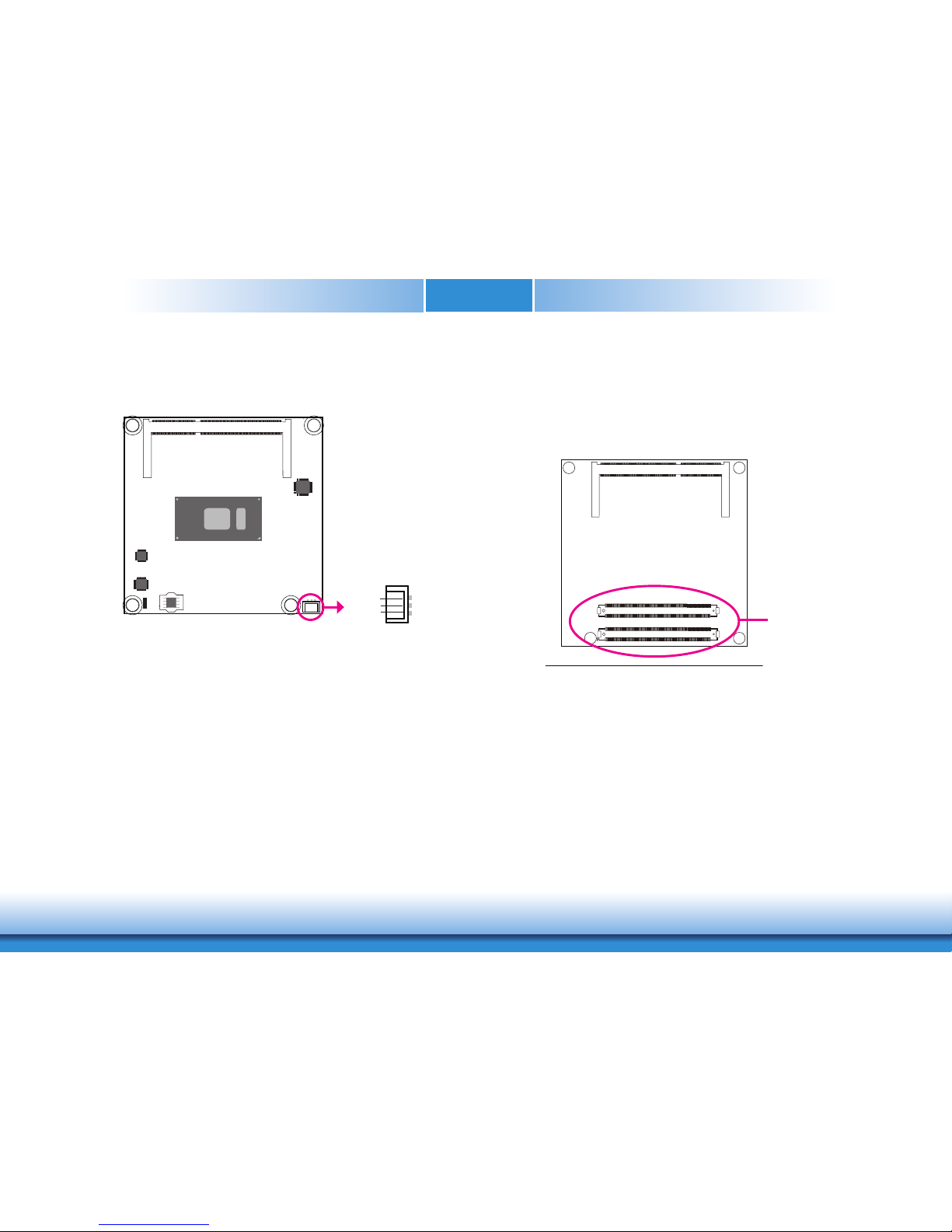
CPU Fan Connector
Connect the CPU fan’s cable connector to the CPU fan connector on the board. The cooling fan
will provide adequate airflow throughout the chassis to prevent overheating the CPU and board
components.
BIOS Setting
“PC Health Status” submenu in the Advanced menu of the BIOS will display the current speed
of the cooling fan. Refer to chapter 4 of the manual for more information.
3
1
Sense
+12V
Ground
COM Express Connectors
The COM Express connectors are used to interface the SU968 COM Express board to a carrier
board. Connect the COM Express connectors (located on the solder side of the board) to the
COM Express connectors on the carrier board.
Refer to the “Installing SU968 onto a Carrier Board” section in this chapter for more information.
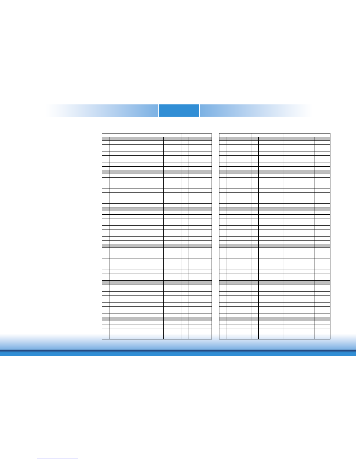
Refer to the following pages for the pin functions of these connectors.
COM Express Connectors
Page 14
www.d.comChapter 3 Hardware Installation
14
Chapter 3
COM Express Connectors
A1 GND (FIXED) B1 GND (FIXED)
A56 PCIE_TX4- B56 P CIE_RX4-
C1 GND (FIXED) D1 GND (FIXED)
C56 NA D56 NA
A2 GBE0_MDI3- B2 GBE0_ACT#
A57 GND B57 GPO2
C2 GND D2 GND
C57 TYPE1# D57 TYPE2#
A3 GBE0_MDI3+ B3 LPC_FRA ME#
A58 PCIE_TX3+ B58 PCIE_RX3+
C3 USB_SSRX0- D3 USB_SSTX0-
C58 NA D58 NA
A4 GBE0_LINK100# B4 LPC_AD0
A59 PCIE_TX3- B59 PCIE_RX3-
C4 USB_SSRX0+ D4 USB_SSTX0+
C59 NA D59 NA
A5 GBE0_LINK1000# B5 LPC_AD1
A60 GND (FIXED) B60 GND (FIXED)
C5 GND D5 GND
C60 GND (FIXED) D60 GND (FIXED)
A6 GBE0_MDI2- B6 LPC_ AD2
A61 PCIE_TX2+ B61 PCIE_RX2+
C6 USB_SSRX1- D6 USB_SSTX1-
C61 NA D61 NA
A7 GBE0_MDI2+ B7 LPC_A D3
A62 PCIE_TX2- B62 PCIE_RX2-
C7 USB_SSRX1+ D7 USB_SSTX1+
C62 NA D62 NA
A8 GBE0_LINK# B8 NA
A63 GPI1 B63 GP O3
C8 GND D8 GND
C63 RSVD
D63 RSVD
A9 GBE0_MDI1- B9 NA A64 PCIE_TX1+ B64 PCIE_RX1+ C9 USB_SSRX2- D9 USB_SSTX2- C64 RSVD D64 RSVD
A10 GBE0_MDI1+ B10 LPC_CLK
A65
PCIE_TX1-
B65
PCIE_RX1- C10 USB_SSRX2+ D10 USB_SSTX2+
C65 NA D65 NA
A11 GND (FIXED) B11 GND (FIXED) A66 GND B66 WAKE0# C11 GND (FIXED) D11 GND (FIXED) C66 NA
D66 NA
A12 GBE0_MDI0- B12 PWRBTN# A67 GPI2
B67 NA
C12 USB_SSRX3- D12 USB_SSTX3-
C67 RSVD
D67 GND
A13 GBE0_MDI0+ B13 SMB_CK A68 PCIE_TX0+
B68 PCIE_RX0+
C13 USB_SSRX3+ D13 USB_SSTX3+
C68 NA
D68
NA
A14 GBE0_CTREF B14 SMB_DAT A69 PCIE_TX0-
B69 PCIE_RX0-
C14 GND D14 GND
C69 NA
D69
NA
A15 SUS_S3# B15 SMB_ALERT# A70 GND(FIXED)
B70 GND (FIXED)
C15 NA D15 DDI1_CTRLCLK_AUX+
C70 GND (FIXED) D70 GND (FIXED)
A16 SATA0_TX+ B16 S ATA1_TX+
A71 LVDS_A0+ B71 LVDS_B0+
C16 NA D16 DDI1_CTRLDATA_AUX-
C71 NA D71 NA
A17 SATA0_TX- B17 S ATA1_TX-
A72 LVDS_A0- B72 LVDS_B0-
C17 RSVD D1 7 RSVD
C72 NA
D72
NA
A18 SUS_S4# B18 SUS_STAT#
A73 LVDS_A1+ B73 LVDS_B1+
C18 RSVD D1 8 RSVD
C73 GND D7 3 GND
A19 SATA0_RX+ B19 SATA1_RX+
A74 LVDS_A1- B74 LVDS_B1-
C19 PCIE_RX6 + D19 PCIE_TX6+
C74 NA D74 NA
A20 SATA0_RX- B20 SATA1_RX-
A75 LVDS_A2+ B75 LVDS_B2+
C20 PCIE_RX6 - D2 0 PCIE_TX6-
C75 NA D75 NA
A21 GND (FIXED) B21 GND (FIXED)
A76 LVDS_A2- B 76 LVDS_B2-
C21 GND (FIXED) D21 GND (FIXED)
C76 GND D76 GND
A22 SATA2_TX+ B22 NA
A77 LVDS_VDD_EN B77 LVDS_B3+
C22 PCIE_RX7 + D22 PCIE_TX7+
C77 RSVD D77 RSVD
A23 SATA2_TX- B23 NA
A78 LVDS_A3+ B78 LVDS_B3-
C23 PCIE_RX7 - D2 3 PCIE_TX7-
C78 NA D78 NA
A24 SUS_S5# B24 PWR_OK
A79 LVDS_A3- B 79 LVDS_BKLT_EN
C24 DDI1_HPD D24 RSVD
C79 NA D79 NA
A25 SATA2_RX+ B25 NA
A80 GND (FIXED) B80 GND (FIXED)
C25 NA D25 RSVD
C80 GND (FIXED) D80 GND (FIXED)
A26 SATA2_RX- B26 NA
A81 LVDS_A_CK+ B81 LVDS_B_CK+
C26 NA D26 DDI1_PAIR0+
C81 NA D81 NA
A27 BATLOW# B27 WDT A82 LVDS_A_CK- B82 LVDS_B_CK- C27 RSVD D27 DDI1_ PAIR0- C82 NA D82 NA
A28 (S)ATA_ACT# B28 NA A83 LVDS_I2C_CK B83 LVDS_BKLT_CTRL C28 RSVD D28 RS VD C83 RSVD D83 RSVD
A29 AC/HDA_SYNC B29 AC/HDA _SDIN1 A84 LVDS_I2C_DAT B84 VCC_5V_SBY C29 NA D2 9 DDI1_PAIR1 + C84 GND D84 GND
A30 AC/HDA _RST# B30 AC/HDA _SDIN0 A85 GPI3 B85 VCC_5V_SBY C30 NA D30 DDI1_PAIR1- C8 5 NA D85 NA
A31 GND (FIXED) B31 GND (FIXED) A86 RSVD B86 VCC_5V_SBY C31 GND (FIXED) D31 GND (FIXED) C86 NA D86 NA
A32 AC/HDA _BITCLK B32 SPKR A87 RSVD B87 VCC_5V_SBY C32 DDI2_ CTRLCLK_AUX+ D32 DDI1_PAIR2+ C87 GND D87 GND
A33 AC/HDA _SDOUT B33 I2C_CK A88
PCIE0_CK_REF+
B88 BIOS_DIS1# C3 3 DDI2_CTRLDATA_AUX- D33 DD I1_PAIR2- C88 NA D88 NA
A34 BIOS_DIS0# B34 I2C_DAT A89
PCIE0_CK_REF-
B89 VGA_RED C34 DDI2_DDC_AUX_SEL D34 DDI1_DDC_AUX_SEL C89 NA D8 9 NA
A35 THRMTRIP# B35 THRM# A90 GND (FIXED) B90 GND (FIXED) C35 RSVD D35 RSVD C90 GND (FIXED) D90 GND (FIXED)
A36 USB6- B36 USB7- A91 SPI_POWER B91 VGA_GRN C36 NA D36 DDI1_PAIR3+ C91 NA D91 NA
A37 USB6+ B37 USB7+ A92 SPI_MISO B92 VGA_BLU C37 NA D37 DDI1_PAIR3 - C9 2 NA D92 NA
A38 USB_6_7_OC# B38 USB_4_5_OC# A93 GPO0 B93 VGA_HSYNC C38 NA D38 RSVD C93 GND D93 GND
A39 USB4- B39 USB5- A94 SPI_CLK B94 VGA_VSYNC C39 NA D39 DDI2_PAIR0+ C94 NA D94 NA
A40 USB4+ B40 USB5+ A95 SPI_MOSI B95 VGA_I2C_CK C40 NA D40 DDI2_PAIR0- C95 NA D95 NA
A41 GND (FIXED) B41 GND (FIXED) A96 TPM_PP B96 VGA_I2C_DAT C41 GND (FIXED) D4 1 GND (FIXED) C96 GND D96 GND
A42 USB2- B42 USB3- A97 TYPE10# B97 SPI_CS# C42 NA D42 DDI2_PAIR1+ C97 RSV D D97 RSVD
A43 USB2+ B43 USB3+ A98 SER0_TX B98 RSVD C43 NA D43 DDI2_PAIR1- C98 NA D98 NA
A44 USB_2_3_OC# B44 USB_0_1_OC# A99 SER0_RX B99 RSVD C44 NA D44 DDI2_HPD C9 9 NA D99 NA
A45 USB0- B45 USB1- A100 GND (FIXED) B100 GND (FIXED) C4 5 RSVD D45 RS VD C100 GND (FIXED) D100 GND (FIXED)
A46 USB0+ B46 USB1+ A101 SER1_ TX B101 FAN_PWMOUT C46 NA D46 DDI2_PAIR2+ C101 NA D101 NA
A47 VCC_RTC B47 EXCD1_PERST# A102 SER1_RX B102 FAN_TA CHIN C47 NA D47 DDI2_PAIR2- C102 NA D102 NA
A48 EXCD0_PERST# B48 EXCD1_CPPE# A103 LID# B103 SLEEP# C48 RSVD D48 RSVD C103 GND D103 GND
A49 EXCD0_CPPE# B49 SYS_RESET# A104 VCC_12V B104 VCC_12V C49 NA D49 DDI2_PAIR3+ C104 VCC_12V D1 04 VCC_12V
A50 LPC_SERIRQ B50 CB_RESET# A105 VCC_12V B105 VCC_12V C50 NA D50 DDI2_PAIR3- C105 VCC_12V D105 VCC_12V
A51 GND (FIXED) B51 GND (FIXED)
A106 VCC_12V B106 VCC_12V
C51 GND (FIXED) D51 GND (FIXED)
C106 VCC_12V D106 VCC_12V
A52 PCIE_TX5+ B52 PCIE_RX5+
A107 VCC_12V B107 VCC_12V
C52 NA D52 NA
C107 VCC_12V D107 VCC_12V
A53 PCIE_TX5- B53 PCIE_RX5-
A108 VCC_12V B108 VCC_12V
C53 NA D53 NA
C108 VCC_12V D108 VCC_12V
A54 GPI0 B54 GPO1
A109 VCC_12V B109 VCC_12V
C54 TYPE0# D54 PEG_LANE_REV#
C109 VCC_12V D109 VCC_12V
A55 PCIE_TX4+ B55 PCIE_RX4+
A110 GND (FIXED) B110 GND (FIXED)
C55 NA D55 NA
C110 GND (FIXED) D110 GND (FIXED)
Row C
Row D
Row A
Row B
Row C
Row D
Row A
Row B
C1 GND (FIXED) D1 GND (FIXED)
C56 NA D56 NA
C2 GND D2 GND
C57 TYPE1# D57 TYPE2#
C3 USB_SSRX0- D3 USB_SSTX0-
C58 NA D58 NA
C4 USB_SSRX0+ D4 USB_SSTX0+
C59 NA D59 NA
C5 GND D5 GND
C60 GND (FIXED) D60 GND (FIXED)
C6 USB_SSRX1- D6 USB_SSTX1-
C61 NA D61 NA
C7 USB_SSRX1+ D7 USB_SSTX1+
C62 NA D62 NA
C8 GND D8 GND
C63 RSVD
D63 RSVD
C65 NA D65 NA
D66 NA
C12 USB_SSRX3- D12 USB_SSTX3-
C67 RSVD
D67 GND
C13 USB_SSRX3+ D13 USB_SSTX3+
C68 NA
D68
NA
C14 GND D14 GND
C69 NA
D69
NA
C15 NA D15 DDI1_CTRLCLK_AUX+
C70 GND (FIXED) D70 GND (FIXED)
C16 NA D16 DDI1_CTRLDATA_AUX-
C71 NA D71 NA
C17 RSVD D1 7 RSVD
C72 NA
D72
NA
C18 RSVD D1 8 RSVD
C73 GND D7 3 GND
C19 PCIE_RX6 + D19 PCIE_TX6+
C74 NA D74 NA
C20 PCIE_RX6 - D2 0 PCIE_TX6-
C75 NA D75 NA
C21 GND (FIXED) D21 GND (FIXED)
C76 GND D76 GND
C22 PCIE_RX7 + D22 PCIE_TX7+
C77 RSVD D77 RSVD
C23 PCIE_RX7 - D2 3 PCIE_TX7-
C78 NA D78 NA
C24 DDI1_HPD D24 RSVD
C79 NA D79 NA
C25 NA D25 RSVD
C80 GND (FIXED) D80 GND (FIXED)
C26 NA D26 DDI1_PAIR0+
C81 NA D81 NA
C51 GND (FIXED) D51 GND (FIXED)
C106 VCC_12V D106 VCC_12V
C52 NA D52 NA
C107 VCC_12V D107 VCC_12V
C53 NA D53 NA
C108 VCC_12V D108 VCC_12V
C54 TYPE0# D54 PEG_LANE_REV#
C109 VCC_12V D109 VCC_12V
C55 NA D55 NA
C110 GND (FIXED) D110 GND (FIXED)
Row C
Row D
Row C
Row D
Page 15
www.d.comChapter 3 Hardware Installation
15
Chapter 3
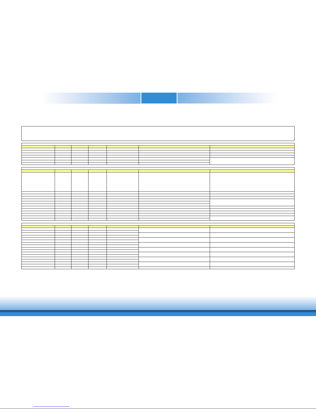
COM Express Connectors Signals and Descriptions
Signal Pin# Module Pin Type Pwr Rail /Tolerance SU968 Carrier Board Description
AC/HAD_RST# A30 O CMOS 3.3V Suspend/3.3V Connect to CODEC pin 11 RESET# Reset output to CODEC, active low.
AC/HDA_SYNC A29 O CMOS 3.3V/3.3V Connect to CODEC pin 10 SYNC Sample-synchronization signal to the CODEC(s).
AC/HDA_BITCLK A32 I/O CMOS 3.3V/3.3V Connect to CODEC pin 6 BIT_CLK Serial data clock generated by the external CODEC(s).
AC/HDA_SDOUT A33 O CMOS 3.3V/3.3V Connect to CODEC pin 5 SDATA_OUT Serial TDM data output to the CODEC.
AC/HDA_SDIN2 B28 I/O CMOS 3.3V Suspend/3.3V NA
AC/HDA_SDIN1 B29 I/O CMOS 3.3V Suspend/3.3V
AC/HDA_SDIN0 B30 I/O CMOS 3.3V Suspend/3.3V Connect 33 Ω in series to CODEC0 pin 8 SDATA_IN
Signal Pin# Module Pin Type Pwr Rail /Tolerance SU968 Carrier Board Description
GBE0_MDI0+ A13 I/O Analog 3.3V max Suspend Connect to Magnetics Module MDI0+/-
Gigabit Ethernet Controller 0: Media Dependent Interface Differential
Pairs 0,1,2,3. The MDI can operate in 1000, 100 and 10 Mbit / sec
modes. Some pairs are unused in some modes, per the following:
1000BASE-T 100BASE-TX 10BASE-T
MDI[0]+/- B1_DA+/- TX+/- TX+/ MDI[1]+/- B1_DB+/- RX+/- RX+/ MDI[2]+/- B1_DC+/-
MDI[3]+/- B1_DD+/GBE0_MDI0- A12 I/O Analog 3.3V max Suspend
GBE0_MDI1+ A10 I/O Analog 3.3V max Suspend Connect to Magnetics Module MDI1+/GBE0_MDI1- A9 I/O Analog 3.3V max Suspend
GBE0_MDI2+ A7 I/O Analog 3.3V max Suspend Connect to Magnetics Module MDI2+/GBE0_MDI2- A6 I/O Analog 3.3V max Suspend
GBE0_MDI3+ A3 I/O Analog 3.3V max Suspend Connect to Magnetics Module MDI3+/GBE0_MDI3- A2 I/O Analog 3.3V max Suspend
GBE0_ACT# B2 OD CMOS 3.3V Suspend/3.3V Connect to LED and recommend current limit resistor 150 Ω to 3.3VSB Gigabit Ethernet Controller 0 activity indicator, active low.
GBE0_LINK# A8 OD CMOS 3.3V Suspend/3.3V NC Gigabit Ethernet Controller 0 link indicator, active low.
GBE0_LINK100# A4 OD CMOS 3.3V Suspend/3.3V Gigabit Ethernet Controller 0 100 Mbit / sec link indicator, active low.
GBE0_LINK100# A4 OD CMOS 3.3V Suspend/3.3V Connect to LED and recommend current limit resistor 150 Ω to 3.3VSB
GBE0_LINK1000# A5 OD CMOS 3.3V Suspend/3.3V Connect to LED and recommend current limit resistor 150 Ω to 3.3VSB
Signal Pin# Module Pin Type Pwr Rail /Tolerance SU968 Carrier Board Description
SATA0_TX+ A16 O SATA AC coupled on Module AC Coupling capacitor
SATA0_TX- A17 O SATA AC coupled on Module AC Coupling capacitor
SATA0_RX+ A19 I SATA AC coupled on Module AC Coupling capacitor
SATA0_RX- A20 I SATA AC coupled on Module AC Coupling capacitor
SATA1_TX+ B16 O SATA AC coupled on Module AC Coupling capacitor
SATA1_TX- B17 O SATA AC coupled on Module AC Coupling capacitor
SATA1_RX+ B19 I SATA AC coupled on Module AC Coupling capacitor
SATA1_RX- B20 I SATA AC coupled on Module AC Coupling capacitor
SATA2_TX+ A22 O SATA AC coupled on Module AC Coupling capacitor
SATA2_TX- A23 O SATA AC coupled on Module AC Coupling capacitor
SATA2_RX+ A25 I SATA AC coupled on Module AC Coupling capacitor
SATA2_RX- A26 I SATA AC coupled on Module AC Coupling capacitor
SATA3_TX+ B22 O SATA AC coupled on Module NA
SATA3_TX- B23 O SATA AC coupled on Module NA
SATA3_RX+ B25 I SATA AC coupled on Module NA
SATA3_RX- B26 I SATA AC coupled on Module NA
ATA_ACT# A28 I/O CMOS 3.3V / 3.3V PU 10K to 3.3V Connect to LED and recommend current limit resistor 220Ω to 3.3V ATA (parallel and serial) or SAS activity indicator, active low.
Pin Types
I Input to the Module
O Output from the Module
I/O Bi-directional input / output signal
OD Open drain output
AC97/HDA Signals and Descriptions
Serial TDM data inputs from up to 2 CODECs.
Gigabit Ethernet Signals and Descriptions
Serial ATA or SAS Channel 0 transmit differential pair.
Connect to SATA0 Conn RX pin Serial ATA or SAS Channel 0 receive differential pair.
Connect to SATA1 Conn TX pin
Connect to SATA2 Conn TX pin
Serial ATA or SAS Channel 3 transmit differential pair.
Serial ATA or SAS Channel 3 receive differential pair.
Connect to SATA2 Conn RX pin Serial ATA or SAS Channel 2 receive differential pair.
Serial ATA or SAS Channel 2 transmit differential pair.
Connect to SATA1 Conn RX pin Serial ATA or SAS Channel 1 receive differential pair.
SATA Signals and Descriptions
Connect to SATA0 Conn TX pin
Serial ATA or SAS Channel 1 transmit differential pair.
Gigabit Ethernet Controller 0 1000 Mbit / sec link indicator, active low.
Page 16
www.d.comChapter 3 Hardware Installation
16
Chapter 3
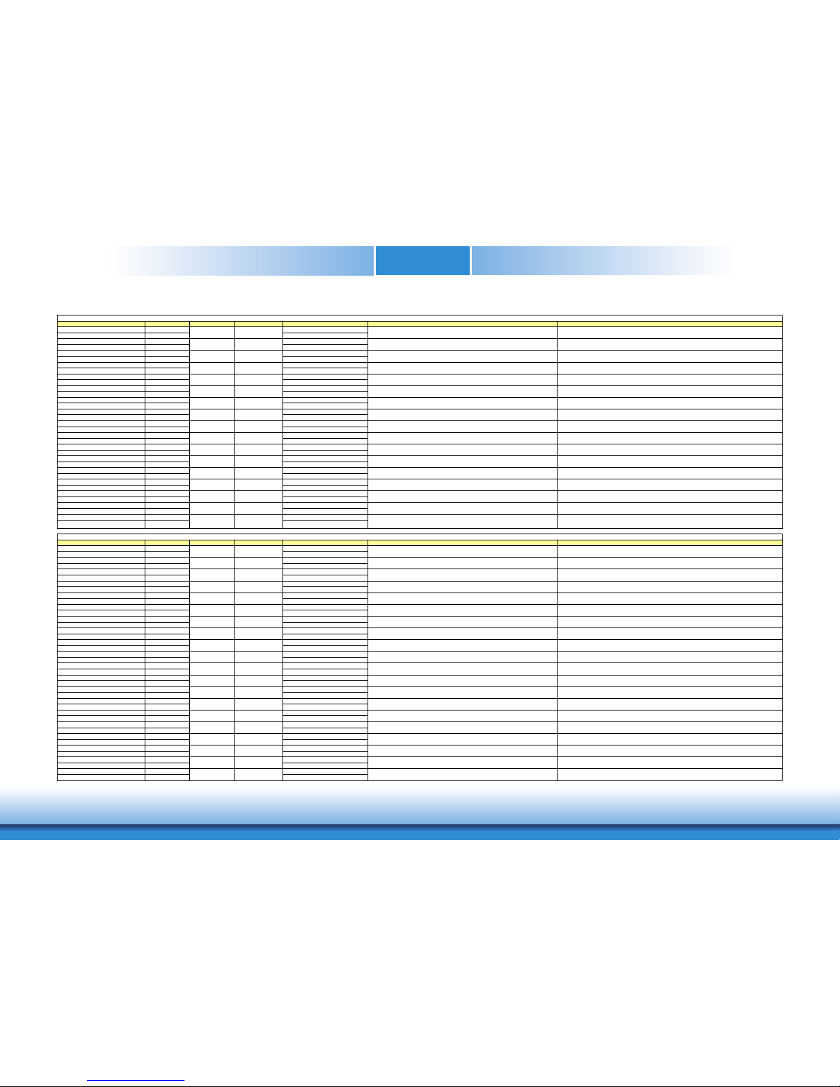
Signal Pin# Module Pin Type Pwr Rail /Tolerance SU968 Carrier Board Description
PCIE_TX0+ A68 AC Coupling capacitor
PCIE_TX0- A69 AC Coupling capacitor
PCIE_RX0+ B68
PCIE_RX0- B69
PCIE_TX1+ A64 AC Coupling capacitor
PCIE_TX1- A65 AC Coupling capacitor
PCIE_RX1+ B64
PCIE_RX1- B65
PCIE_TX2+ A61 AC Coupling capacitor
PCIE_TX2- A62 AC Coupling capacitor
PCIE_RX2+ B61
PCIE_RX2- B62
PCIE_TX3+ A58 AC Coupling capacitor
PCIE_TX3- A59 AC Coupling capacitor
PCIE_RX3+ B58
PCIE_RX3- B59
PCIE_TX4+ A55 AC Coupling capacitor
PCIE_TX4- A56 AC Coupling capacitor
PCIE_RX4+ B55
PCIE_RX4- B56
PCIE_TX5+ A52 AC Coupling capacitor
PCIE_TX5- A53 AC Coupling capacitor
PCIE_RX5+ B52
PCIE_RX5- B53
PCIE_TX6+ D19 AC Coupling capacitor
PCIE_TX6- D20 AC Coupling capacitor
PCIE_RX6+ C19
PCIE_RX6- C20
PCIE_TX7+ D22 AC Coupling capacitor
PCIE_TX7- D23 AC Coupling capacitor
PCIE_RX7+ C22
PCIE_RX7- C23
PCIE0_CK_REF+ A88
PCIE0_CK_REF- A89
Connect to PCIE device or slot
Device - Connect AC Coupling cap 0.1uF
Slot - Connect to PCIE Conn pin
Connect to PCIE device or slot
Device - Connect AC Coupling cap 0.1uF
Slot - Connect to PCIE Conn pin
Connect to PCIE device or slot
Device - Connect AC Coupling cap 0.1uF
Slot - Connect to PCIE Conn pin
Connect to PCIE device or slot
Device - Connect AC Coupling cap 0.1uF
Slot - Connect to PCIE Conn pin
Connect to PCIE device or slot
Device - Connect AC Coupling cap 0.1uF
Slot - Connect to PCIE Conn pin
Connect to PCIE device or slot
I PCIE AC coupled off Module
I PCIE AC coupled off Module
O PCIE AC coupled on Module
PCI Express Differential Receive Pairs 7
O PCIE PCIE Connect to PCIE device, PCIe CLK Buffer or slot
Reference clock output for all PCI Express and PCI Express Graphics
lanes.
PCI Express Differential Receive Pairs 6
O PCIE AC coupled on Module PCI Express Differential Transmit Pairs 7
PCI Express Differential Transmit Pairs 4
PCI Express Differential Receive Pairs 2
PCI Express Differential Transmit Pairs 6
PCI Express Differential Transmit Pairs 3
I PCIE AC coupled off Module PCI Express Differential Receive Pairs 5
I PCIE AC coupled off Module
O PCIE AC coupled on Module PCI Express Differential Transmit Pairs 5
I PCIE AC coupled off Module PCI Express Differential Receive Pairs 4
O PCIE AC coupled on Module
O PCIE AC coupled on Module
Device - Connect AC Coupling cap 0.1uF
Slot - Connect to PCIE Conn pin
Connect to PCIE device or slot
Device - Connect AC Coupling cap 0.1uF
Slot - Connect to PCIE Conn pin
Connect to PCIE device or slot
Device - Connect AC Coupling cap 0.1uF
Slot - Connect to PCIE Conn pin
AC coupled on Module PCI Express Differential Transmit Pairs 1
PCI Express Differential Receive Pairs 1
PCI Express Differential Receive Pairs 3
O PCIE AC coupled on Module PCI Express Differential Transmit Pairs 0
O PCIE AC coupled on Module PCI Express Differential Transmit Pairs 2
I PCIE AC coupled off Module
I PCIE AC coupled off Module PCI Express Differential Receive Pairs 0
I PCIE AC coupled off Module
O PCIE
PCI Express Lanes Signals and Descriptions
Signal Pin# Module Pin Type Pwr Rail /Tolerance SU968 Carrier Board Description
PEG_TX0+ D52 NA
PEG_TX0- D53 NA
PEG_RX0+ C52 NA
PEG_RX0- C53 NA
PEG_TX1+ D55 NA
PEG_TX1- D56 NA
PEG_RX1+ C55 NA
PEG_RX1- C56 NA
PEG_TX2+ D58 NA
PEG_TX2- D59 NA
PEG_RX2+ C58 NA
PEG_RX2- C59 NA
PEG_TX3+ D61 NA
PEG_TX3- D62 NA
PEG_RX3+ C61 NA
PEG_RX3- C62 NA
PEG_TX4+ D65 NA
PEG_TX4- D66 NA
PEG_RX4+ C65 NA
PEG_RX4- C66 NA
PEG_TX5+ D68 NA
PEG_TX5- D69 NA
PEG_RX5+ C68 NA
PEG_RX5- C69 NA
PEG_TX6+ D71 NA
PEG_TX6- D72 NA
PEG_RX6+ C71 NA
PEG_RX6- C72 NA
PEG_TX7+ D74 NA
PEG_TX7- D75 NA
PEG_RX7+ C74 NA
PEG_RX7- C75 NA
PEG_TX8+ D78 NA
PEG_TX8- D79 NA
PEG_RX8+ C78 NA
PEG_RX8- C79 NA
PEG_TX9+ D81 NA
PEG_TX9- D82 NA
PEG_RX9+ C81 NA
PEG_RX9- C82 NA
I PCIE AC coupled off Module PCI Express Graphics receive differential pairs 8
I PCIE AC coupled off Module PCI Express Graphics receive differential pairs 9
O PCIE AC coupled on Module PCI Express Graphics transmit differential pairs 9
O PCIE AC coupled on Module PCI Express Graphics transmit differential pairs 8
I PCIE AC coupled off Module PCI Express Graphics receive differential pairs 5
O PCIE
O PCIE AC coupled on Module PCI Express Graphics transmit differential pairs 6
O PCIE AC coupled on Module PCI Express Graphics transmit differential pairs 5
I PCIE AC coupled off Module PCI Express Graphics receive differential pairs 7
AC coupled on Module PCI Express Graphics transmit differential pairs 7
I PCIE AC coupled off Module PCI Express Graphics receive differential pairs 6
PCI Express Graphics transmit differential pairs 4
I PCIE AC coupled off Module
I PCIE AC coupled off Module PCI Express Graphics receive differential pairs 3
I PCIE AC coupled off Module PCI Express Graphics receive differential pairs 2
O PCIE AC coupled on Module PCI Express Graphics transmit differential pairs 3
PCI Express Graphics receive differential pairs 4
O PCIE AC coupled on Module
O PCIE AC coupled on Module
I PCIE
PCI Express Graphics transmit differential pairs 2
PEG Signals and Descriptions
O PCIE AC coupled on Module PCI Express Graphics transmit differential pairs 0
I PCIE AC coupled off Module PCI Express Graphics receive differential pairs 0
O PCIE AC coupled on Module PCI Express Graphics transmit differential pairs 1
AC coupled off Module PCI Express Graphics receive differential pairs 1
Page 17
www.d.comChapter 3 Hardware Installation
17
Chapter 3
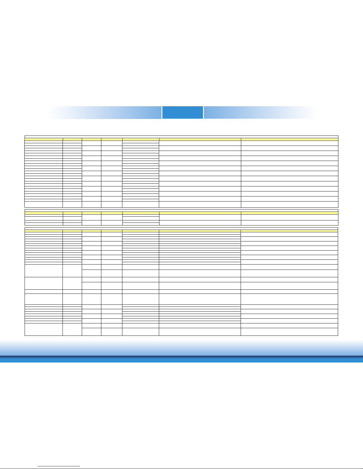
Signal Pin# Module Pin Type Pwr Rail /Tolerance SU968 Carrier Board Description
PEG Signals and Descriptions
Signal Pin# Module Pin Type Pwr Rail /Tolerance SU968 Carrier Board Description
PEG_TX0+ D52 NA
PEG_TX0- D53 NA
PEG_RX0+ C52 NA
PEG_RX0- C53 NA
PEG_TX1+ D55 NA
PEG_TX1- D56 NA
PEG_RX1+ C55 NA
PEG_RX1- C56 NA
PEG_TX2+ D58 NA
PEG_TX2- D59 NA
PEG_RX2+ C58 NA
PEG_RX2- C59 NA
PEG_TX3+ D61 NA
PEG_TX3- D62 NA
PEG_RX3+ C61 NA
PEG_RX3- C62 NA
PEG_TX4+ D65 NA
PEG_TX4- D66 NA
PEG_RX4+ C65 NA
PEG_RX4- C66 NA
PEG_TX5+ D68 NA
PEG_TX5- D69 NA
PEG_RX5+ C68 NA
PEG_RX5- C69 NA
PEG_TX6+ D71 NA
PEG_TX6- D72 NA
PEG_RX6+ C71 NA
PEG_RX6- C72 NA
PEG_TX7+ D74 NA
PEG_TX7- D75 NA
PEG_RX7+ C74 NA
PEG_RX7- C75 NA
PEG_TX8+ D78 NA
PEG_TX8- D79 NA
PEG_RX8+ C78 NA
PEG_RX8- C79 NA
PEG_TX9+ D81 NA
PEG_TX9- D82 NA
PEG_RX9+ C81 NA
PEG_RX9- C82 NA
PEG_TX10+ D85 NA
PEG_TX10- D86 NA
PEG_RX10+ C85 NA
PEG_RX10- C86 NA
PEG_TX11+ D88 NA
PEG_TX11- D89 NA
PEG_RX11+ C88 NA
PEG_RX11- C89 NA
PEG_TX12+ D91 NA
PEG_TX12- D92 NA
PEG_RX12+ C91 NA
PEG_RX12- C92 NA
PEG_TX13+ D94 NA
PEG_TX13- D95 NA
PEG_RX13+ C94 NA
PEG_RX13- C95 NA
PEG_TX14+ D98 NA
PEG_TX14- D99 NA
PEG_RX14+ C98 NA
PEG_RX14- C99 NA
PEG_TX15+ D101 NA
PEG_TX15- D102 NA
PEG_RX15+ C101 NA
PEG_RX15- C102 NA
PEG_LANE_RV# D54 I CMOS 3.3V / 3.3V PU 10K to 3.3V
PCI Express Graphics lane reversal input strap. Pull low on the Carrier
board to reverse lane order.
I PCIE AC coupled off Module
PCI Express Graphics receive differential pairs 14
PCI Express Graphics receive differential pairs 12
O PCIE AC coupled on Module PCI Express Graphics transmit differential pairs 14
I PCIE AC coupled off Module PCI Express Graphics receive differential pairs 15
I PCIE AC coupled off Module PCI Express Graphics receive differential pairs 13
O PCIE AC coupled on Module PCI Express Graphics transmit differential pairs 15
I PCIE AC coupled off Module
O PCIE AC coupled on Module PCI Express Graphics transmit differential pairs 13
O PCIE AC coupled on Module PCI Express Graphics transmit differential pairs 12
O PCIE AC coupled on Module PCI Express Graphics transmit differential pairs 11
I PCIE AC coupled off Module
I PCIE AC coupled off Module PCI Express Graphics receive differential pairs 11
PCI Express Graphics receive differential pairs 10
I PCIE AC coupled off Module PCI Express Graphics receive differential pairs 8
O PCIE AC coupled on Module PCI Express Graphics transmit differential pairs 10
I PCIE AC coupled off Module PCI Express Graphics receive differential pairs 9
O PCIE AC coupled on Module PCI Express Graphics transmit differential pairs 9
O PCIE AC coupled on Module PCI Express Graphics transmit differential pairs 8
I PCIE AC coupled off Module PCI Express Graphics receive differential pairs 5
O PCIE
O PCIE AC coupled on Module PCI Express Graphics transmit differential pairs 6
O PCIE AC coupled on Module PCI Express Graphics transmit differential pairs 5
I PCIE AC coupled off Module PCI Express Graphics receive differential pairs 7
AC coupled on Module PCI Express Graphics transmit differential pairs 7
I PCIE AC coupled off Module PCI Express Graphics receive differential pairs 6
PCI Express Graphics transmit differential pairs 4
I PCIE AC coupled off Module
I PCIE AC coupled off Module PCI Express Graphics receive differential pairs 3
I PCIE AC coupled off Module PCI Express Graphics receive differential pairs 2
O PCIE AC coupled on Module PCI Express Graphics transmit differential pairs 3
PCI Express Graphics receive differential pairs 4
O PCIE AC coupled on Module
O PCIE AC coupled on Module
I PCIE
PCI Express Graphics transmit differential pairs 2
PEG Signals and Descriptions
O PCIE AC coupled on Module PCI Express Graphics transmit differential pairs 0
I PCIE AC coupled off Module PCI Express Graphics receive differential pairs 0
O PCIE AC coupled on Module PCI Express Graphics transmit differential pairs 1
AC coupled off Module PCI Express Graphics receive differential pairs 1
Signal Pin# Module Pin Type Pwr Rail /Tolerance SU968 Carrier Board Description
EXCD0_CPPE# A49 PU 10k to 3.3V
EXCD1_CPPE# B48 PU 10k to 3.3V
EXCD0_PERST# A48
EXCD1_PERST# B47
O CMOS 3.3V /3.3V PCI ExpressCard: reset, active low, one per card
ExpressCard Signals and Descriptions
I CMOS 3.3V /3.3V
PCI ExpressCard: PCI Express capable card request, active low, one per
card
Signal Pin# Module Pin Type Pwr Rail /Tolerance SU968 Carrier Board Description
DDI1_PAIR0+/SDVO1_RED+ D26 Connect AC Coupling Capacitors 0.1uF to Device
DDI1_PAIR0-/SDVO1_RED- D27 Connect AC Coupling Capacitors 0.1uF to Device
DDI1_PAIR1+/SDVO1_GRN+ D29 Connect AC Coupling Capacitors 0.1uF to Device
DDI1_PAIR1-/SDVO1_GRN- D30 Connect AC Coupling Capacitors 0.1uF to Device
DDI1_PAIR2+/SDVO1_BLU+ D32 Connect AC Coupling Capacitors 0.1uF to Device
DDI1_PAIR2-/SDVO1_BLU- D33 Connect AC Coupling Capacitors 0.1uF to Device
DDI1_PAIR3+/SDVO1_CK+ D36 Connect AC Coupling Capacitors 0.1uF to Device
DDI1_PAIR3-/SDVO1_CK- D37 Connect AC Coupling Capacitors 0.1uF to Device
DDI1_PAIR4+/SDVO1_INT+ C25 NA
DDI1_PAIR4-/SDVO1_INT- C26 NA
DDI1_PAIR5+/SDVO1_TVCLKIN+
C29 NA
DDI1_PAIR5-/SDVO1_TVCLKIN- C30 NA
DDI1_PAIR6+/SDVO1_FLDSTALL+ C15 NA
DDI1_PAIR6-/SDVO1_FLDSTALL- C16 NA
I/O PCIE AC coupled on Module
PD 100K to GND
(S/W IC between Rpu/PCH)
Connect to DP AUX+ DP AUX+ function if DDI1_DDC_AUX_SEL is no connect
I/O OD CMOS 3.3V / 3.3V
PU 4.7K to 3.3V, PD 100K to GND
(S/W IC between Rpu/Rpd resistor)
Connect to HDMI/DVI I2C CTRLCLK HDMI/DVI I2C CTRLCLK if DDI1_DDC_AUX_SEL is pulled high
I/O PCIE AC coupled on Module
PU 100K to 3.3V
(S/W IC between Rpu/PCH)
Connect to DP AUX- DP AUX- function if DDI1_DDC_AUX_SEL is no connect
I/O OD CMOS 3.3V / 3.3V
PU 4.7K to 3.3V/PU 100K to 3.3V
(S/W IC between 4.7K/100K
resistor)
Connect to HDMI/DVI I2C CTRLDATA HDMI/DVI I2C CTRLDATA if DDI1_DDC_AUX_SEL is pulled high
DDI1_HPD C24 I CMOS 3.3V / 3.3V PD 1M and Connect to device Hot Plug Detect DDI Hot-Plug Detect
DDI1_DDC_AUX_SEL D34 I CMOS 3.3V / 3.3V PD 1M to GND PU 100K to 3.3V for DDC(HDMI/DVI)
Selects the function of DDI1_CTRLCLK_AUX+ and DDI1_CTRLDATA_AUX-.
DDI[n]_DDC_AUX_SEL shall be pulled to 3.3V on the Carrier with a 100K Ohm
resistor to configure the DDI[n]_AUX pair as the DDC channel.
Carrier DDI[n]_DDC_AUX_SEL should be connected to pin 13 of the DisplayPort
DDI2_PAIR0+ D39 Connect AC Coupling Capacitors 0.1uF to Device
DDI2_PAIR0- D40 Connect AC Coupling Capacitors 0.1uF to Device
DDI2_PAIR1+ D42 Connect AC Coupling Capacitors 0.1uF to Device
DDI2_PAIR1- D43 Connect AC Coupling Capacitors 0.1uF to Device
DDI2_PAIR2+ D46 Connect AC Coupling Capacitors 0.1uF to Device
DDI2_PAIR2- D47 Connect AC Coupling Capacitors 0.1uF to Device
DDI2_PAIR3+ D49 Connect AC Coupling Capacitors 0.1uF to Device
DDI2_PAIR3- D50 Connect AC Coupling Capacitors 0.1uF to Device
I/O PCIE AC coupled on Module
PD 100K to GND
(S/W IC between Rpu/PCH)
Connect to DP AUX+ DP AUX+ function if DDI2_DDC_AUX_SEL is no connect
I/O OD CMOS 3.3V / 3.3V
PU 4.7K to 3.3V, PD 100K to GND
(S/W IC between Rpu/Rpd resistor)
Connect to HDMI/DVI I2C CTRLCLK HDMI/DVI I2C CTRLCLK if DDI2_DDC_AUX_SEL is pulled high
AC coupled off Module Serial Digital Video Field Stall input differential pair.
O PCIE
O PCIE AC coupled off Module DDI 1 Pair 3 differential pairs/Serial Digital Video B clock output differential pair.
I PCIE
I PCIE AC coupled off Module Serial Digital Video TVOUT synchronization clock input differential pair.
AC coupled off Module
O PCIE AC coupled off Module
O PCIE AC coupled off Module DDI 2 Pair 3 differential pairs
DDI 2 Pair 0 differential pairs
DDI Signals and Descriptions
O PCIE AC coupled off Module DDI 1 Pair 0 differential pairs/Serial Digital Video B red output differential pair
I PCIE
O PCIE AC coupled off Module DDI 2 Pair 2 differential pairs
O PCIE AC coupled off Module DDI 2 Pair 1 differential pairs
DDI2_CTRLCLK_AUX+ C32
DDI1_CTRLCLK_AUX+/SDVO1_CTRLCLK D15
DDI1_CTRLCLK_AUX-/SDVO1_CTRLDATA D16
AC coupled off Module DDI 1 Pair 2 differential pairs/Serial Digital Video B blue output differential pair
O PCIE AC coupled off Module DDI 1 Pair 1 differential pairs/Serial Digital Video B green output differential pair
Serial Digital Video B interrupt input differential pair.
Page 18
www.d.comChapter 3 Hardware Installation
18
Chapter 3
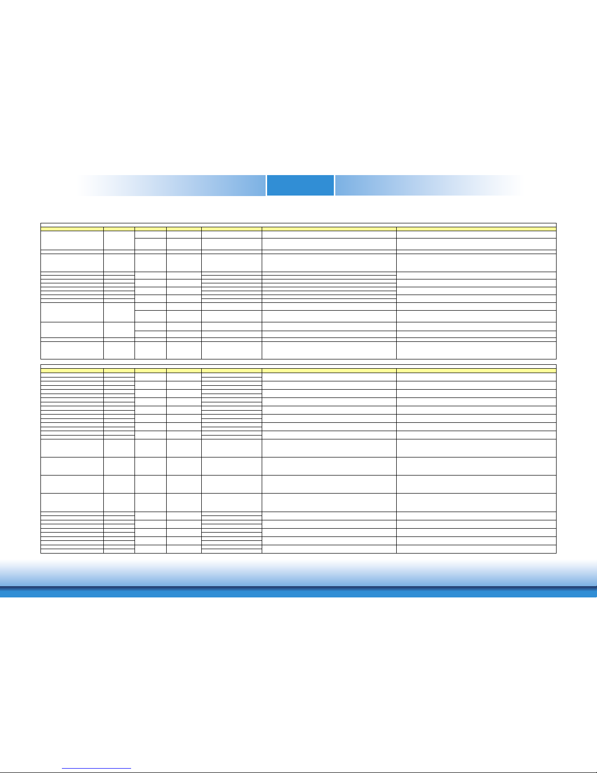
Signal Pin# Module Pin Type Pwr Rail /Tolerance SU968 Carrier Board Description
DDI Signals and Descriptions
Signal Pin# Module Pin Type Pwr Rail /Tolerance SU968 Carrier Board Description
DDI1_PAIR0+/SDVO1_RED+ D26 Connect AC Coupling Capacitors 0.1uF to Device
DDI1_PAIR0-/SDVO1_RED- D27 Connect AC Coupling Capacitors 0.1uF to Device
DDI1_PAIR1+/SDVO1_GRN+ D29 Connect AC Coupling Capacitors 0.1uF to Device
DDI1_PAIR1-/SDVO1_GRN- D30 Connect AC Coupling Capacitors 0.1uF to Device
DDI1_PAIR2+/SDVO1_BLU+ D32 Connect AC Coupling Capacitors 0.1uF to Device
DDI1_PAIR2-/SDVO1_BLU- D33 Connect AC Coupling Capacitors 0.1uF to Device
DDI1_PAIR3+/SDVO1_CK+ D36 Connect AC Coupling Capacitors 0.1uF to Device
DDI1_PAIR3-/SDVO1_CK- D37 Connect AC Coupling Capacitors 0.1uF to Device
DDI1_PAIR4+/SDVO1_INT+ C25 NA
DDI1_PAIR4-/SDVO1_INT- C26 NA
DDI1_PAIR5+/SDVO1_TVCLKIN+
C29 NA
DDI1_PAIR5-/SDVO1_TVCLKIN- C30 NA
DDI1_PAIR6+/SDVO1_FLDSTALL+ C15 NA
DDI1_PAIR6-/SDVO1_FLDSTALL- C16 NA
I/O PCIE AC coupled on Module
PD 100K to GND
(S/W IC between Rpu/PCH)
Connect to DP AUX+ DP AUX+ function if DDI1_DDC_AUX_SEL is no connect
I/O OD CMOS 3.3V / 3.3V
PU 4.7K to 3.3V, PD 100K to GND
(S/W IC between Rpu/Rpd resistor)
Connect to HDMI/DVI I2C CTRLCLK HDMI/DVI I2C CTRLCLK if DDI1_DDC_AUX_SEL is pulled high
I/O PCIE AC coupled on Module
PU 100K to 3.3V
(S/W IC between Rpu/PCH)
Connect to DP AUX- DP AUX- function if DDI1_DDC_AUX_SEL is no connect
I/O OD CMOS 3.3V / 3.3V
PU 4.7K to 3.3V/PU 100K to 3.3V
(S/W IC between 4.7K/100K
resistor)
Connect to HDMI/DVI I2C CTRLDATA HDMI/DVI I2C CTRLDATA if DDI1_DDC_AUX_SEL is pulled high
DDI1_HPD C24 I CMOS 3.3V / 3.3V PD 1M and Connect to device Hot Plug Detect DDI Hot-Plug Detect
DDI1_DDC_AUX_SEL D34 I CMOS 3.3V / 3.3V PD 1M to GND PU 100K to 3.3V for DDC(HDMI/DVI)
Selects the function of DDI1_CTRLCLK_AUX+ and DDI1_CTRLDATA_AUX-.
DDI[n]_DDC_AUX_SEL shall be pulled to 3.3V on the Carrier with a 100K Ohm
resistor to configure the DDI[n]_AUX pair as the DDC channel.
Carrier DDI[n]_DDC_AUX_SEL should be connected to pin 13 of the DisplayPort
DDI2_PAIR0+ D39 Connect AC Coupling Capacitors 0.1uF to Device
DDI2_PAIR0- D40 Connect AC Coupling Capacitors 0.1uF to Device
DDI2_PAIR1+ D42 Connect AC Coupling Capacitors 0.1uF to Device
DDI2_PAIR1- D43 Connect AC Coupling Capacitors 0.1uF to Device
DDI2_PAIR2+ D46 Connect AC Coupling Capacitors 0.1uF to Device
DDI2_PAIR2- D47 Connect AC Coupling Capacitors 0.1uF to Device
DDI2_PAIR3+ D49 Connect AC Coupling Capacitors 0.1uF to Device
DDI2_PAIR3- D50 Connect AC Coupling Capacitors 0.1uF to Device
I/O PCIE AC coupled on Module
PD 100K to GND
(S/W IC between Rpu/PCH)
Connect to DP AUX+ DP AUX+ function if DDI2_DDC_AUX_SEL is no connect
I/O OD CMOS 3.3V / 3.3V
PU 4.7K to 3.3V, PD 100K to GND
(S/W IC between Rpu/Rpd resistor)
Connect to HDMI/DVI I2C CTRLCLK HDMI/DVI I2C CTRLCLK if DDI2_DDC_AUX_SEL is pulled high
I/O PCIE AC coupled on Module
PU 100K to 3.3V
(S/W IC between Rpu/PCH)
Connect to DP AUX- DP AUX- function if DDI2_DDC_AUX_SEL is no connect
I/O OD CMOS
3.3V / 3.3V
PU 4.7K to 3.3V/PU 100K to 3.3V
(S/W IC between 4.7K/100K
resistor)
Connect to HDMI/DVI I2C CTRLDATA HDMI/DVI I2C CTRLDATA if DDI2_DDC_AUX_SEL is pulled high
DDI2_HPD D44 I CMOS 3.3V / 3.3V PD 1M and Connect to device Hot Plug Detect DDI Hot-Plug Detect
DDI2_DDC_AUX_SEL C34 I CMOS 3.3V / 3.3V PD 1M to GND PU 100K to 3.3V for DDC(HDMI/DVI)
Selects the function of DDI2_CTRLCLK_AUX+ and DDI2_CTRLDATA_AUX-.
DDI[n]_DDC_AUX_SEL shall be pulled to 3.3V on the Carrier with a 100K Ohm
resistor to configure the DDI[n]_AUX pair as the DDC channel.
Carrier DDI[n]_DDC_AUX_SEL should be connected to pin 13 of the DisplayPort
DDI3_PAIR0+ C39 NA
DDI3_PAIR0- C40 NA
DDI3_PAIR1+ C42 NA
DDI3_PAIR1- C43 NA
DDI3_PAIR2+ C46 NA
DDI3_PAIR2- C47 NA
DDI3_PAIR3+ C49 NA
DDI3_PAIR3- C50 NA
I/O PCIE AC coupled on Module NA DP AUX+ function if DDI3_DDC_AUX_SEL is no connect
I/O OD CMOS 3.3V / 3.3V NA HDMI/DVI I2C CTRLCLK if DDI3_DDC_AUX_SEL is pulled high
I/O PCIE AC coupled on Module NA DP AUX- function if DDI3_DDC_AUX_SEL is no connect
I/O OD CMOS 3.3V / 3.3V NA HDMI/DVI I2C CTRLDATA if DDI3_DDC_AUX_SEL is pulled high
DDI3_HPD C44 I CMOS 3.3V / 3.3V NA DDI Hot-Plug Detect
DDI3_DDC_AUX_SEL C38 I CMOS 3.3V / 3.3V NA
Selects the function of DDI3_CTRLCLK_AUX+ and DDI3_CTRLDATA_AUX-.
DDI[n]_DDC_AUX_SEL shall be pulled to 3.3V on the Carrier with a 100K Ohm
resistor to configure the DDI[n]_AUX pair as the DDC channel.
Carrier DDI[n]_DDC_AUX_SEL should be connected to pin 13 of the DisplayPort
AC coupled off Module Serial Digital Video Field Stall input differential pair.
O PCIE
O PCIE AC coupled off Module DDI 1 Pair 3 differential pairs/Serial Digital Video B clock output differential pair.
I PCIE
I PCIE AC coupled off Module Serial Digital Video TVOUT synchronization clock input differential pair.
AC coupled off Module
O PCIE AC coupled off Module
DDI 3 Pair 0 differential pairs
O PCIE AC coupled off Module DDI 2 Pair 3 differential pairs
DDI 3 Pair 2 differential pairs
O PCIE DDI 3 Pair 1 differential pairs
DDI3_CTRLCLK_AUX+ C36
DDI3_CTRLCLK_AUX- C37
O PCIE AC coupled off Module
DDI 2 Pair 0 differential pairs
O PCIE AC coupled off Module DDI 3 Pair 3 differential pairs
AC coupled off Module
DDI Signals and Descriptions
O PCIE AC coupled off Module DDI 1 Pair 0 differential pairs/Serial Digital Video B red output differential pair
I PCIE
O PCIE AC coupled off Module DDI 2 Pair 2 differential pairs
O PCIE AC coupled off Module DDI 2 Pair 1 differential pairs
O PCIE AC coupled off Module
DDI2_CTRLCLK_AUX+ C32
DDI2_CTRLCLK_AUX- C33
DDI1_CTRLCLK_AUX+/SDVO1_CTRLCLK D15
DDI1_CTRLCLK_AUX-/SDVO1_CTRLDATA D16
AC coupled off Module DDI 1 Pair 2 differential pairs/Serial Digital Video B blue output differential pair
O PCIE AC coupled off Module DDI 1 Pair 1 differential pairs/Serial Digital Video B green output differential pair
Serial Digital Video B interrupt input differential pair.
Signal Pin# Module Pin Type Pwr Rail /Tolerance SU968 Carrier Board Description
USB0+ A46
USB0- A45
USB1+ B46
USB1- B45
USB2+ A43
USB2- A42
USB3+ B43
USB3- B42
USB4+ A40
USB4- A39
USB5+ B40
USB5- B39
USB6+ A37
USB6- A36
USB7+ B37
USB7- B36
USB_0_1_OC# B44 I CMOS 3.3V Suspend/3.3V PU 10k to 3V3_DU Connect to Overcurrent of USB Power Switch
USB over-current sense, USB channels 0 and 1. A pull-up for this line
shall be present on the Module. An open drain driver from a USB
current monitor on the Carrier Board may drive this line low. Do not
pull this line high on the Carrier Board.
USB_2_3_OC# A44 I CMOS 3.3V Suspend/3.3V PU 10k to 3V3_DU Connect to Overcurrent of USB Power Switch
USB over-current sense, USB channels 2 and 3. A pull-up for this line
shall be present on the Module. An open drain driver from a USB
current monitor on the Carrier Board may drive this line low. Do not
pull this line high on the Carrier Board.
USB_4_5_OC# B38 I CMOS 3.3V Suspend/3.3V PU 10k to 3V3_DU Connect to Overcurrent of USB Power Switch
USB over-current sense, USB channels 4 and 5. A pull-up for this line
shall be present on the Module. An open drain driver from a USB
current monitor on the Carrier Board may drive this line low. Do not
pull this line high on the Carrier Board.
USB_6_7_OC# A38 I CMOS 3.3V Suspend/3.3V PU 10k to 3V3_DU Connect to Overcurrent of USB Power Switch
USB over-current sense, USB channels 6 and 7. A pull-up for this line
shall be present on the Module. An open drain driver from a USB
current monitor on the Carrier Board may drive this line low. Do not
pull this line high on the Carrier Board.
USB_SSTX0+ D4 AC Coupling capacitor
USB_SSTX0- D3 AC Coupling capacitor
USB_SSRX0+ C4
USB_SSRX0- C3
USB_SSTX1+ D7 AC Coupling capacitor
USB_SSTX1- D6 AC Coupling capacitor
USB_SSRX1+ C7
USB_SSRX1- C6
USB_SSTX2+ D10 AC Coupling capacitor
USB_SSTX2- D9 AC Coupling capacitor
O PCIE AC coupled on Module
Connect 90Ω @100MHz Common Choke in series and ESD suppressors to GND to USB
connector
Additional transmit signal differential pairs for the SuperSpeed USB data path.
I PCIE AC coupled off Modul
Connect 90Ω @100MHz Common Choke in series and ESD suppressors to GND to USB
connector
Additional receive signal differential pairs for the SuperSpeed USB data path.
O PCIE AC coupled on Module
Connect 90Ω @100MHz Common Choke in series and ESD suppressors to GND to USB
connector
Additional transmit signal differential pairs for the SuperSpeed USB data path.
I PCIE AC coupled off Modul
Connect 90Ω @100MHz Common Choke in series and ESD suppressors to GND to USB
connector
Additional receive signal differential pairs for the SuperSpeed USB data path.
O PCIE AC coupled on Module
Connect 90Ω @100MHz Common Choke in series and ESD suppressors to GND to USB
connector
Additional transmit signal differential pairs for the SuperSpeed USB data path.
I/O USB 3.3V Suspend/3.3V
Connect 90Ω @100MHz Common Choke in series and ESD suppressors to GND to USB
connector
USB differential pairs 7
I/O USB
I/O USB 3.3V Suspend/3.3V
Connect 90Ω @100MHz Common Choke in series and ESD suppressors to GND to USB
connector
USB differential pairs 2
I/O USB 3.3V Suspend/3.3V
Connect 90Ω @100MHz Common Choke in series and ESD suppressors to GND to USB
connector
USB differential pairs 1
I/O USB 3.3V Suspend/3.3V
Connect 90Ω @100MHz Common Choke in series and ESD suppressors to GND to USB
connector
USB differential pairs 6
3.3V Suspend/3.3V
Connect 90Ω @100MHz Common Choke in series and ESD suppressors to GND to USB
connector
USB differential pairs 4
I/O USB 3.3V Suspend/3.3V
Connect 90Ω @100MHz Common Choke in series and ESD suppressors to GND to USB
connector
USB differential pairs 3
I/O USB 3.3V Suspend/3.3V
Connect 90Ω @100MHz Common Choke in series and ESD suppressors to GND to USB
connector
USB differential pairs 5
USB Signals and Descriptions
I/O USB 3.3V Suspend/3.3V
Connect 90Ω @100MHz Common Choke in series and ESD suppressors to GND to USB
connector
USB differential pairs 0
Page 19
www.d.comChapter 3 Hardware Installation
19
Chapter 3
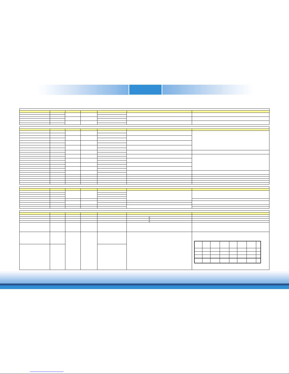
Signal Pin# Module Pin Type Pwr Rail /Tolerance SU968 Carrier Board Description
USB0+ A46
USB0- A45
USB1+ B46
USB1- B45
USB2+ A43
USB2- A42
USB3+ B43
USB3- B42
USB4+ A40
USB4- A39
USB5+ B40
USB5- B39
USB6+ A37
USB6- A36
USB7+ B37
USB7- B36
USB_0_1_OC# B44 I CMOS 3.3V Suspend/3.3V PU 10k to 3V3_DU Connect to Overcurrent of USB Power Switch
USB over-current sense, USB channels 0 and 1. A pull-up for this line
shall be present on the Module. An open drain driver from a USB
current monitor on the Carrier Board may drive this line low. Do not
pull this line high on the Carrier Board.
USB_2_3_OC# A44 I CMOS 3.3V Suspend/3.3V PU 10k to 3V3_DU Connect to Overcurrent of USB Power Switch
USB over-current sense, USB channels 2 and 3. A pull-up for this line
shall be present on the Module. An open drain driver from a USB
current monitor on the Carrier Board may drive this line low. Do not
pull this line high on the Carrier Board.
USB_4_5_OC# B38 I CMOS 3.3V Suspend/3.3V PU 10k to 3V3_DU Connect to Overcurrent of USB Power Switch
USB over-current sense, USB channels 4 and 5. A pull-up for this line
shall be present on the Module. An open drain driver from a USB
current monitor on the Carrier Board may drive this line low. Do not
pull this line high on the Carrier Board.
USB_6_7_OC# A38 I CMOS 3.3V Suspend/3.3V PU 10k to 3V3_DU Connect to Overcurrent of USB Power Switch
USB over-current sense, USB channels 6 and 7. A pull-up for this line
shall be present on the Module. An open drain driver from a USB
current monitor on the Carrier Board may drive this line low. Do not
pull this line high on the Carrier Board.
USB_SSTX0+ D4 AC Coupling capacitor
USB_SSTX0- D3 AC Coupling capacitor
USB_SSRX0+ C4
USB_SSRX0- C3
USB_SSTX1+ D7 AC Coupling capacitor
USB_SSTX1- D6 AC Coupling capacitor
USB_SSRX1+ C7
USB_SSRX1- C6
USB_SSTX2+ D10 AC Coupling capacitor
USB_SSTX2- D9 AC Coupling capacitor
USB_SSRX2+ C10
USB_SSRX2- C9
USB_SSTX3+ D13 AC Coupling capacitor
USB_SSTX3- D12 AC Coupling capacitor
USB_SSRX3+ C13
USB_SSRX3- C12
O PCIE AC coupled on Module
Connect 90Ω @100MHz Common Choke in series and ESD suppressors to GND to USB
connector
Additional transmit signal differential pairs for the SuperSpeed USB data path.
I PCIE AC coupled off Modul
Connect 90Ω @100MHz Common Choke in series and ESD suppressors to GND to USB
connector
Additional receive signal differential pairs for the SuperSpeed USB data path.
O PCIE AC coupled on Module
Connect 90Ω @100MHz Common Choke in series and ESD suppressors to GND to USB
connector
Additional transmit signal differential pairs for the SuperSpeed USB data path.
I PCIE AC coupled off Modul
Connect 90Ω @100MHz Common Choke in series and ESD suppressors to GND to USB
connector
Additional receive signal differential pairs for the SuperSpeed USB data path.
O PCIE AC coupled on Module
Connect 90Ω @100MHz Common Choke in series and ESD suppressors to GND to USB
connector
Additional transmit signal differential pairs for the SuperSpeed USB data path.
I PCIE AC coupled off Modul
I/O USB 3.3V Suspend/3.3V
Connect 90Ω @100MHz Common Choke in series and ESD suppressors to GND to USB
connector
USB differential pairs 7
Connect 90Ω @100MHz Common Choke in series and ESD suppressors to GND to USB
connector
Additional receive signal differential pairs for the SuperSpeed USB data path.
O PCIE
AC coupled on Module
Connect 90Ω @100MHz Common Choke in series and ESD suppressors to GND to USB
connector
Additional transmit signal differential pairs for the SuperSpeed USB data path.
I PCIE AC coupled off Modul
Connect 90Ω @100MHz Common Choke in series and ESD suppressors to GND to USB
connector
Additional receive signal differential pairs for the SuperSpeed USB data path.
I/O USB
I/O USB 3.3V Suspend/3.3V
Connect 90Ω @100MHz Common Choke in series and ESD suppressors to GND to USB
connector
USB differential pairs 2
I/O USB 3.3V Suspend/3.3V
Connect 90Ω @100MHz Common Choke in series and ESD suppressors to GND to USB
connector
USB differential pairs 1
I/O USB 3.3V Suspend/3.3V
Connect 90Ω @100MHz Common Choke in series and ESD suppressors to GND to USB
connector
USB differential pairs 6
3.3V Suspend/3.3V
Connect 90Ω @100MHz Common Choke in series and ESD suppressors to GND to USB
connector
USB differential pairs 4
I/O USB 3.3V Suspend/3.3V
Connect 90Ω @100MHz Common Choke in series and ESD suppressors to GND to USB
connector
USB differential pairs 3
I/O USB 3.3V Suspend/3.3V
Connect 90Ω @100MHz Common Choke in series and ESD suppressors to GND to USB
connector
USB differential pairs 5
USB Signals and Descriptions
I/O USB 3.3V Suspend/3.3V
Connect 90Ω @100MHz Common Choke in series and ESD suppressors to GND to USB
connector
USB differential pairs 0
Signal Pin# Module Pin Type Pwr Rail /Tolerance SU968 Carrier Board Description
USB Signals and Descriptions
Signal Pin# Module Pin Type Pwr Rail /Tolerance SU968 Carrier Board Description
LVDS_A0+ A71
LVDS_A0- A72
LVDS_A1+ A73
LVDS_A1- A74
LVDS_A2+ A75
LVDS_A2- A76
LVDS_A3+ A78
LVDS_A3- A79
LVDS_A_CK+ A81
LVDS_A_CK- A82
LVDS_B0+ B71
LVDS_B0- B72
LVDS_B1+ B73
LVDS_B1- B74
LVDS_B2+ B75
LVDS_B2- B76
LVDS_B3+ B77
LVDS_B3- B78
LVDS_B_CK+ B81
LVDS_B_CK- B82
LVDS_VDD_EN A77 O CMOS 3.3V / 3.3V Connect to enable control of LVDS panel power circuit LVDS panel power enable
LVDS_BKLT_EN B79 O CMOS 3.3V / 3.3V Connect to enable control of LVDS panel backlight power circuit. LVDS panel backlight enable
LVDS_BKLT_CTRL B83 O CMOS 3.3V / 3.3V Connect to brightness control of LVDS panel backlight power circuit. LVDS panel backlight brightness control
LVDS_I2C_CK A83 I/O OD CMOS 3.3V / 3.3V PU 4.7K to 3.3V Connect to DDC clock of LVDS panel I2C clock output for LVDS display use
LVDS_I2C_DAT A84 I/O OD CMOS 3.3V / 3.3V PU 4.7K to 3.3V Connect to DDC data of LVDS panel I2C data line for LVDS display use
Signal Pin# Module Pin Type Pwr Rail /Tolerance SU968 Carrier Board Description
LPC_AD0 B4
LPC_AD1 B5
LPC_AD2 B6
LPC_AD3 B7
LPC_FRAME# B3 O CMOS 3.3V / 3.3V LPC frame indicates the start of an LPC cycle
LPC_DRQ0# B8 PU 10K to 3.3V NC
LPC_DRQ1# B9 PU 10K to 3.3V NC
LPC_SERIRQ A50 I/O CMOS 3.3V / 3.3V PU 10K to 3.3V LPC serial interrupt
LPC_CLK B10 O CMOS 3.3V / 3.3V LPC clock output - 24MHz nominal
Signal
Pin# Module Pin Type Pwr Rail /Tolerance SU968 Carrier Board Description
SPI_CS# B97 O CMOS 3.3V Suspend/3.3V
Connect to Carrier Board SPI Device CS# pin
Chip select for Carrier Board SPI - may be sourced from chipset SPI0 or SPI1
SPI_MISO A92 I CMOS 3.3V Suspend/3.3V Connect a series resistor 33Ω
to Carrier Board SPI Device SO pin Data in to Module from Carrier SPI
SPI_MOSI A95 O CMOS 3.3V Suspend/3.3V Connect a series resistor 33 Ω
to Carrier Board SPI Device SI pin Data out from Module to Carrier SPI
SPI_CLK A94 O CMOS 3.3V Suspend/3.3V Connect a series resistor 33Ω
to Carrier Board SPI Device SCK pin Clock from Module to Carrier SPI
SPI_POWER A91 O 3.3V Suspend/3.3V
Power supply for Carrier Board SPI – sourced from Module – nominally
3.3V. The Module shall provide a minimum of 100mA on SPI_POWER.
Carriers shall use less than 100mA of SPI_POWER. SPI_POWER
shall only be used to power SPI devices on the Carrier
BIOS_DIS0# A34
BIOS_DIS1# B88
Connect to LPC device
Connect to LPC device
Selection straps to determine the BIOS boot device.
The Carrier should only float these or pull them low, please refer to
COM Express Module Base Specification Revision 2.1 for strapping options of BIOS disable signals.
LVDS Channel B differential clock
LPC Signals and Descriptions
3.3V / 3.3V LPC serial DMA request
SPI Signals and Descriptions
O LVDS LVDS
Connect to LVDS connector
O LVDS LVDS
Connect to LVDS connector
I/O CMOS 3.3V / 3.3V
NA
O LVDS LVDS
LVDS
Connect to LVDS connector
O LVDS LVDS
LPC multiplexed address, command and data bus
O LVDS LVDS
Connect to LVDS connector
LVDS Channel B differential pairs
Ther LVDS flat panel differential pairs (LVDS_A[0:3]+/-, LVDS_B[0:3]+/-. LVDS_A_CK+/-,
LVDS_B_CK+/-) shall have 100Ω terminations across the pairs at the destination. These
terminations may be on the Carrier Board if the Carrier Board implements a LVDS deserializer
on-board
O LVDS LVDS
Connect to LVDS connector
Connect to LVDS connector
LVDS Channel A differential clockO LVDS LVDS
Connect to LVDS connector
I CMOS
I CMOS
LVDS Signals and Descriptions
O LVDS LVDS
Connect to LVDS connector LVDS Channel A differential pairs
Ther LVDS flat panel differential pairs (LVDS_A[0:3]+/-, LVDS_B[0:3]+/-. LVDS_A_CK+/-,
LVDS_B_CK+/-) shall have 100Ω terminations across the pairs at the destination. These
terminations may be on the Carrier Board if the Carrier Board implements a LVDS deserializer
on-board
O LVDS
Connect to LVDS connector
O LVDS LVDS
Connect to LVDS connector
Ref
Line
Bios
Entry
SPI
Descriptor
Carrier
SPI_CS#
Chipset
SPI CS0#
Destination
Chipset
SPI CS1#
Destination
BIOS
DIS0#
BIOS
DIS1#
1
1
1
1
00
0
0
ModuleModule SPI0/SPI1
SPI1
(Default)
SPI0
High
High
CarrierCarrier
Carri er
(Default)
Module
(Default)
Module
Module
Module
(Default)
Module
ModuleModule
3
2
1
0
Carrier FWH
SPI0/SPI1
(Default)
SPI0/SPI1
Page 20
www.d.comChapter 3 Hardware Installation
20
Chapter 3
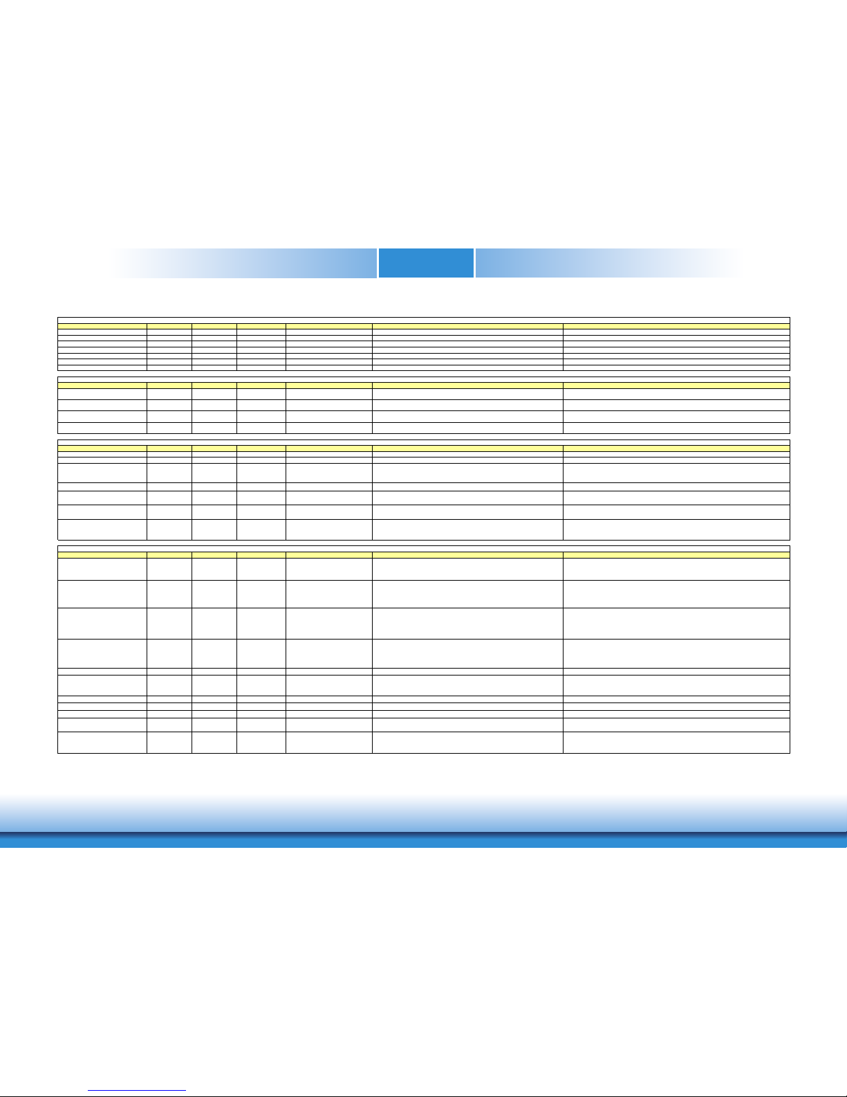
Signal Pin# Module Pin Type Pwr Rail /Tolerance SU968 Carrier Board Description
VGA_RED B89 O Analog Analog PD 150 to GND PD 150R,connect to VGA connector with EMI filter & ESD protect component. Red for monitor. Analog output
VGA_GRN B91 O Analog Analog PD 150 to GND PD 150R,connect to VGA connector with EMI filter & ESD protect component. Green for monitor. Analog output
VGA_BLU B92 O Analog Analog PD 150 to GND PD 150R,connect to VGA connector with EMI filter & ESD protect component. Blue for monitor. Analog output
VGA_HSYNC B93 O CMOS 3.3V / 3.3V Connect to VGA connector with a3.3V Buffer IC to isolate PCH & Display Device Horizontal sync output to VGA monitor
VGA_VSYNC B94 O CMOS 3.3V / 3.3V Connect to VGA connector with a 33V Buffer IC to isolate PCH & Display Device Vertical sync output to VGA monitor
VGA_I2C_CK B95 I/O OD CMOS 3.3V / 3.3V PU 2.2K to 3.3V Connect to VGA connector with a 3.3V to 5V Level shift circuit. DDC clock line (I2C port dedicated to identify VGA monitor capabilities)
VGA_I2C_DAT B96 I/O OD CMOS 3.3V / 3.3V PU 2.2K to 3.3V Connect to VGA connector with a 3.3V to 5V Level shift circuit. DDC data line.
Signal Pin# Module Pin Type Pwr Rail /Tolerance SU968 Carrier Board Description
SER0_TX A98 O CMOS 3.3V/5V PD 4.7K to GND
General purpose serial port 0 transmitter
(Recommend add Protecting Logic Level Signals on Pins Reclaimed from VCC_12V)
SER0_RX A99 I CMOS 3.3V/5V PU 10K to 3.3V
General purpose serial port 0 receiver
(Recommend add Protecting Logic Level Signals on Pins Reclaimed from VCC_12V)
SER1_TX A101 O CMOS 3.3V/5V PD 4.7K to GND
General purpose serial port 1 transmitter
(Recommend add Protecting Logic Level Signals on Pins Reclaimed from VCC_12V)
SER1_RX A102 I CMOS 3.3V/5V PU 10K to 3.3V
General purpose serial port 1 receiver
(Recommend add Protecting Logic Level Signals on Pins Reclaimed from VCC_12V)
Signal Pin# Module Pin Type Pwr Rail /Tolerance SU968 Carrier Board Description
I2C_CK
B33 I/O OD CMOS 3.3V Suspend/3.3V PU 2.2K to 3V3_DU_EC General purpose I2C port clock output
I2C_DAT B34 I/O OD CMOS 3.3V Suspend/3.3V PU 2.2K to 3V3_DU_EC General purpose I2C port data I/O line
SPKR B32 O CMOS 3.3V / 3.3V
Output for audio enunciator - the "speaker" in PC-AT systems.
This port provides the PC beep signal and is mostly intended for
debugging purposes.
WDT B27 O CMOS 3.3V / 3.3V Output indicating that a watchdog time-out event has occurred.
FAN_PWNOUT B101 O OD CMOS 3.3V / 3.3V
Fan speed control. Uses the Pulse Width Modulation (PWM) technique to control the fan's RPM.
(Recommend add Protecting Logic Level Signals on Pins Reclaimed from VCC_12V)
FAN_TACHIN B102 I OD CMOS 3.3V / 3.3V PU 47K to 3V3
Fan tachometer input for a fan with a two pulse output.
(Recommend add Protecting Logic Level Signals on Pins Reclaimed from VCC_12V)
TPM_PP A96 I CMOS 3.3V / 3.3V
Trusted Platform Module (TPM) Physical Presence pin. Active high.
TPM chip has an internal pull down. This signal is used to indicate
Physical Presence to the TPM.
Signal Pin# Module Pin Type Pwr Rail /Tolerance SU968 Carrier Board Description
PWRBTN# B12 I CMOS 3.3V Suspend/3.3V PU 10K to 3V3_DU_EC PU 4.7K to 3V3_SB
A falling edge creates a power button event. Power button events can
be used to bring a system out of S5 soft off and other suspend states,
as well as powering the system down.
SYS_RESET# B49 I CMOS 3.3V Suspend/3.3V PU 10K to 3V3_DU NC PU 4.7K to 3V3_SB
Reset button input. Active low request for Module to reset and reboot.
May be falling edge sensitive. For situations when SYS_RESET# is
not able to reestablish control of the system, PWR_OK or a power
cycle may be used.
CB_RESET# B50 O CMOS 3.3V Suspend/3.3V PD 100K to GND
Reset output from Module to Carrier Board. Active low. Issued by
Module chipset and may result from a low SYS_RESET# input, a low
PWR_OK input, a VCC_12V power input that falls below the minimum
specification, a watchdog timeout, or may be initiated by the Module
software.
PWR_OK B24 I CMOS 3.3V / 3.3V PU 10K to 3V3
Power OK from main power supply. A high value indicates that the
power is good. This signal can be used to hold off Module startup to
allow Carrier based FPGAs or other configurable devices time to be
programmed.
SUS_STAT# B18 O CMOS 3.3V Suspend/3.3V Indicates imminent suspend operation; used to notify LPC devices.
SUS_S3# A15 O CMOS 3.3V Suspend/3.3V PD 100K to GND
Indicates system is in Suspend to RAM state. Active low output. An
inverted copy of SUS_S3# on the Carrier Board may be used to
enable the non-standby power on a typical ATX supply.
SUS_S4# A18 O CMOS 3.3V Suspend/3.3V PD 100K to GND Indicates system is in Suspend to Disk state. Active low output.
SUS_S5# A24 O CMOS 3.3V Suspend/3.3V PD 100K to GND Indicates system is in Soft Off state.
WAKE0# B66 I CMOS 3.3V Suspend/3.3V PU 1K to 3V3_DU PCI Express wake up signal.
WAKE1# B67 I CMOS 3.3V Suspend/3.3V NA
General purpose wake up signal. May be used to implement wake-up
on PS2 keyboard or mouse activity.
BATLOW# A27 I CMOS 3.3V Suspend/ 3.3V PU 10K to 3V3_DU
Indicates that external battery is low.
This port provides a battery-low signal to the Module for orderly
transitioning to power saving or power cut-off ACPI modes.
Power and System Management Signals and Descriptions
VGA Signals and Descriptions
Serial Interface Signals and Descriptions
Miscellaneous Signal and Descriptions
Page 21
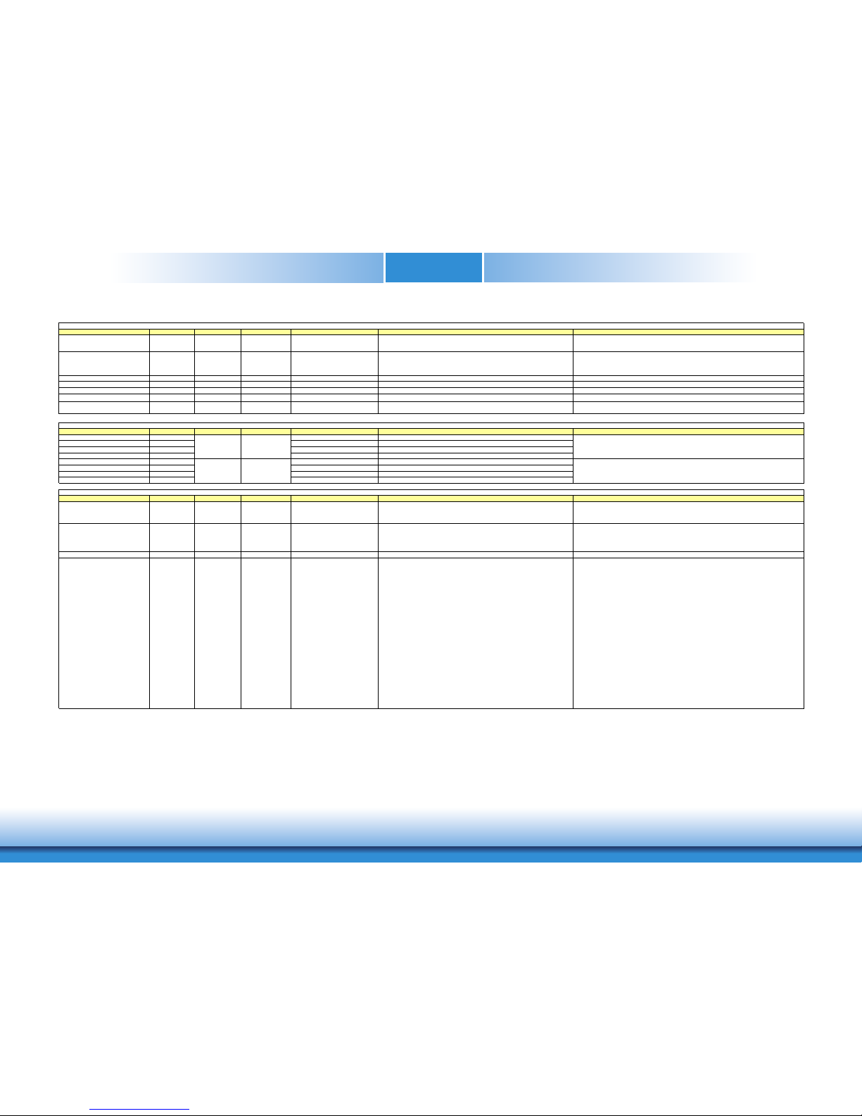
www.d.comChapter 3 Hardware Installation
21
Chapter 3
Signal Pin# Module Pin Type Pwr Rail /Tolerance SU968 Carrier Board Description
VGA_RED B89 O Analog Analog PD 150 to GND PD 150R,connect to VGA connector with EMI filter & ESD protect component. Red for monitor. Analog output
VGA_GRN B91 O Analog Analog PD 150 to GND PD 150R,connect to VGA connector with EMI filter & ESD protect component. Green for monitor. Analog output
VGA_BLU B92 O Analog Analog PD 150 to GND PD 150R,connect to VGA connector with EMI filter & ESD protect component. Blue for monitor. Analog output
VGA_HSYNC B93 O CMOS 3.3V / 3.3V Connect to VGA connector with a3.3V Buffer IC to isolate PCH & Display Device Horizontal sync output to VGA monitor
VGA_VSYNC B94 O CMOS 3.3V / 3.3V Connect to VGA connector with a 33V Buffer IC to isolate PCH & Display Device Vertical sync output to VGA monitor
VGA_I2C_CK B95 I/O OD CMOS 3.3V / 3.3V PU 2.2K to 3.3V Connect to VGA connector with a 3.3V to 5V Level shift circuit. DDC clock line (I2C port dedicated to identify VGA monitor capabilities)
VGA_I2C_DAT B96 I/O OD CMOS 3.3V / 3.3V PU 2.2K to 3.3V Connect to VGA connector with a 3.3V to 5V Level shift circuit. DDC data line.
Signal Pin# Module Pin Type Pwr Rail /Tolerance SU968 Carrier Board Description
SER0_TX A98 O CMOS 3.3V/5V PD 4.7K to GND
General purpose serial port 0 transmitter
(Recommend add Protecting Logic Level Signals on Pins Reclaimed from VCC_12V)
SER0_RX A99 I CMOS 3.3V/5V PU 10K to 3.3V
General purpose serial port 0 receiver
(Recommend add Protecting Logic Level Signals on Pins Reclaimed from VCC_12V)
SER1_TX A101 O CMOS 3.3V/5V PD 4.7K to GND
General purpose serial port 1 transmitter
(Recommend add Protecting Logic Level Signals on Pins Reclaimed from VCC_12V)
SER1_RX A102 I CMOS 3.3V/5V PU 10K to 3.3V
General purpose serial port 1 receiver
(Recommend add Protecting Logic Level Signals on Pins Reclaimed from VCC_12V)
Signal Pin# Module Pin Type Pwr Rail /Tolerance SU968 Carrier Board Description
I2C_CK
B33 I/O OD CMOS 3.3V Suspend/3.3V PU 2.2K to 3V3_DU_EC General purpose I2C port clock output
I2C_DAT B34 I/O OD CMOS 3.3V Suspend/3.3V PU 2.2K to 3V3_DU_EC General purpose I2C port data I/O line
SPKR B32 O CMOS 3.3V / 3.3V
Output for audio enunciator - the "speaker" in PC-AT systems.
This port provides the PC beep signal and is mostly intended for
debugging purposes.
WDT B27 O CMOS 3.3V / 3.3V Output indicating that a watchdog time-out event has occurred.
FAN_PWNOUT B101 O OD CMOS 3.3V / 3.3V
Fan speed control. Uses the Pulse Width Modulation (PWM) technique to control the fan's RPM.
(Recommend add Protecting Logic Level Signals on Pins Reclaimed from VCC_12V)
FAN_TACHIN B102 I OD CMOS 3.3V / 3.3V PU 47K to 3V3
Fan tachometer input for a fan with a two pulse output.
(Recommend add Protecting Logic Level Signals on Pins Reclaimed from VCC_12V)
TPM_PP A96 I CMOS 3.3V / 3.3V
Trusted Platform Module (TPM) Physical Presence pin. Active high.
TPM chip has an internal pull down. This signal is used to indicate
Physical Presence to the TPM.
Signal Pin# Module Pin Type Pwr Rail /Tolerance SU968 Carrier Board Description
PWRBTN# B12 I CMOS 3.3V Suspend/3.3V PU 10K to 3V3_DU_EC PU 4.7K to 3V3_SB
A falling edge creates a power button event. Power button events can
be used to bring a system out of S5 soft off and other suspend states,
as well as powering the system down.
SYS_RESET# B49 I CMOS 3.3V Suspend/3.3V PU 10K to 3V3_DU NC PU 4.7K to 3V3_SB
Reset button input. Active low request for Module to reset and reboot.
May be falling edge sensitive. For situations when SYS_RESET# is
not able to reestablish control of the system, PWR_OK or a power
cycle may be used.
CB_RESET# B50 O CMOS 3.3V Suspend/3.3V PD 100K to GND
Reset output from Module to Carrier Board. Active low. Issued by
Module chipset and may result from a low SYS_RESET# input, a low
PWR_OK input, a VCC_12V power input that falls below the minimum
specification, a watchdog timeout, or may be initiated by the Module
software.
PWR_OK B24 I CMOS 3.3V / 3.3V PU 10K to 3V3
Power OK from main power supply. A high value indicates that the
power is good. This signal can be used to hold off Module startup to
allow Carrier based FPGAs or other configurable devices time to be
programmed.
SUS_STAT# B18 O CMOS 3.3V Suspend/3.3V Indicates imminent suspend operation; used to notify LPC devices.
SUS_S3# A15 O CMOS 3.3V Suspend/3.3V PD 100K to GND
Indicates system is in Suspend to RAM state. Active low output. An
inverted copy of SUS_S3# on the Carrier Board may be used to
enable the non-standby power on a typical ATX supply.
SUS_S4# A18 O CMOS 3.3V Suspend/3.3V PD 100K to GND Indicates system is in Suspend to Disk state. Active low output.
SUS_S5# A24 O CMOS 3.3V Suspend/3.3V PD 100K to GND Indicates system is in Soft Off state.
WAKE0# B66 I CMOS 3.3V Suspend/3.3V PU 1K to 3V3_DU PCI Express wake up signal.
WAKE1# B67 I CMOS 3.3V Suspend/3.3V NA
General purpose wake up signal. May be used to implement wake-up
on PS2 keyboard or mouse activity.
BATLOW# A27 I CMOS 3.3V Suspend/ 3.3V PU 10K to 3V3_DU
Indicates that external battery is low.
This port provides a battery-low signal to the Module for orderly
transitioning to power saving or power cut-off ACPI modes.
LID# A103 I OD CMOS 3.3V Suspend/12V PU 47K to 3V3_DU_EC
LID switch. Low active signal used by the ACPI operating system for a LID switch.
(Recommend add Protecting Logic Level Signals on Pins Reclaimed from VCC_12V)
SLEEP# B103 I OD CMOS 3.3V Suspend/12V PU 10K to 3V3_DU
Sleep button. Low active signal used by the ACPI operating system to bring the
system to sleep state or to wake it up again.
(Recommend add Protecting Logic Level Signals on Pins Reclaimed from VCC_12V)
THRM# B35 I CMOS 3.3V / 3.3V PU 4.7K to 3V3 Input from off-Module temp sensor indicating an over-temp situation.
THRMTRIP# A35 O CMOS 3.3V / 3.3V PU 10K to 3.3V Active low output indicating that the CPU has entered thermal shutdown.
SMB_CK B13 I/O OD CMOS 3.3V Suspend/3.3V PU 2.2K to 3V3_DU_EC System Management Bus bidirectional clock line.
SMB_DAT B14 I/O OD CMOS 3.3V Suspend/3.3V PU 2.2K to 3V3_DU_EC System Management Bus bidirectional data line.
SMB_ALERT# B15 I CMOS 3.3V Suspend/3.3V PU 2.2K to 3V3_DU_EC
System Management Bus Alert – active low input can be used to
generate an SMI# (System Management Interrupt) or to wake the system.
Power and System Management Signals and Descriptions
VGA Signals and Descriptions
Serial Interface Signals and Descriptions
Miscellaneous Signal and Descriptions
Signal Pin# Module Pin Type Pwr Rail /Tolerance SU968 Carrier Board Description
VGA_RED B89 O Analog Analog PD 150 to GND PD 150R,connect to VGA connector with EMI filter & ESD protect component. Red for monitor. Analog output
VGA_GRN B91 O Analog Analog PD 150 to GND PD 150R,connect to VGA connector with EMI filter & ESD protect component. Green for monitor. Analog output
VGA_BLU B92 O Analog Analog PD 150 to GND PD 150R,connect to VGA connector with EMI filter & ESD protect component. Blue for monitor. Analog output
VGA_HSYNC B93 O CMOS 3.3V / 3.3V Connect to VGA connector with a3.3V Buffer IC to isolate PCH & Display Device Horizontal sync output to VGA monitor
VGA_VSYNC B94 O CMOS 3.3V / 3.3V Connect to VGA connector with a 33V Buffer IC to isolate PCH & Display Device Vertical sync output to VGA monitor
VGA_I2C_CK B95 I/O OD CMOS 3.3V / 3.3V PU 2.2K to 3.3V Connect to VGA connector with a 3.3V to 5V Level shift circuit. DDC clock line (I2C port dedicated to identify VGA monitor capabilities)
VGA_I2C_DAT B96 I/O OD CMOS 3.3V / 3.3V PU 2.2K to 3.3V Connect to VGA connector with a 3.3V to 5V Level shift circuit. DDC data line.
Signal Pin# Module Pin Type Pwr Rail /Tolerance SU968 Carrier Board Description
SER0_TX A98 O CMOS 3.3V/5V PD 4.7K to GND
General purpose serial port 0 transmitter
(Recommend add Protecting Logic Level Signals on Pins Reclaimed from VCC_12V)
SER0_RX A99 I CMOS 3.3V/5V PU 10K to 3.3V
General purpose serial port 0 receiver
(Recommend add Protecting Logic Level Signals on Pins Reclaimed from VCC_12V)
SER1_TX A101 O CMOS 3.3V/5V PD 4.7K to GND
General purpose serial port 1 transmitter
(Recommend add Protecting Logic Level Signals on Pins Reclaimed from VCC_12V)
SER1_RX A102 I CMOS 3.3V/5V PU 10K to 3.3V
General purpose serial port 1 receiver
(Recommend add Protecting Logic Level Signals on Pins Reclaimed from VCC_12V)
Signal Pin# Module Pin Type Pwr Rail /Tolerance SU968 Carrier Board Description
I2C_CK
B33 I/O OD CMOS 3.3V Suspend/3.3V PU 2.2K to 3V3_DU_EC General purpose I2C port clock output
I2C_DAT B34 I/O OD CMOS 3.3V Suspend/3.3V PU 2.2K to 3V3_DU_EC General purpose I2C port data I/O line
SPKR B32 O CMOS 3.3V / 3.3V
Output for audio enunciator - the "speaker" in PC-AT systems.
This port provides the PC beep signal and is mostly intended for
debugging purposes.
WDT B27 O CMOS 3.3V / 3.3V Output indicating that a watchdog time-out event has occurred.
FAN_PWNOUT B101 O OD CMOS 3.3V / 3.3V
Fan speed control. Uses the Pulse Width Modulation (PWM) technique to control the fan's RPM.
(Recommend add Protecting Logic Level Signals on Pins Reclaimed from VCC_12V)
FAN_TACHIN B102 I OD CMOS 3.3V / 3.3V PU 47K to 3V3
Fan tachometer input for a fan with a two pulse output.
(Recommend add Protecting Logic Level Signals on Pins Reclaimed from VCC_12V)
TPM_PP A96 I CMOS 3.3V / 3.3V
Trusted Platform Module (TPM) Physical Presence pin. Active high.
TPM chip has an internal pull down. This signal is used to indicate
Physical Presence to the TPM.
Signal Pin# Module Pin Type Pwr Rail /Tolerance SU968 Carrier Board Description
Power and System Management Signals and Descriptions
VGA Signals and Descriptions
Serial Interface Signals and Descriptions
Miscellaneous Signal and Descriptions
Signal Pin# Module Pin Type Pwr Rail /Tolerance SU968 Carrier Board Description
GPO0 A93
GPO1 B54
GPO2 B57
GPO3 B63
GPI0 A54 PU 100K to 3.3V
GPI1 A63 PU 100K to 3.3V
GPI2 A67 PU 100K to 3.3V
GPI3 A85 PU 100K to 3.3V
Signal Pin# Module Pin Type Pwr Rail /Tolerance SU968 Carrier Board Description
VCC_12V
A
104~A109
B104~B109
C104~C109
~
Power Primary power input: +12V nominal. All available VCC_12V pins on the connector(s) shall be used.
VCC_5V_SBY B84~B87 Power
Standby power input: +5.0V nominal. If VCC5_SBY is used, all
available VCC_5V_SBY pins on the connector(s) shall be used. Only
used for standby and suspend functions. May be left unconnected if
these functions are not used in the system design.
VCC_RTC A47 Power Real-time clock circuit-power input. Nominally +3.0V.
GND
A1, A11, A21, A31,
A41, A51, A57, A60,
A66, A70, A80, A90,
A100, A110, B1,
B11, B21 ,B31, B41,
B51, B60, B70, B80,
B90, B100, B110,
C1, C2, C5, C8, C11,
C14, C21, C31, C41,
C51, C60, C70, C73,
C76, C80, C84, C87,
C90, C93, C96,
C100, C103, C110,
D1, D2, D5, D8,
D11, D14, D21, D31,
D51, D60, D67, D70,
D73, D76, D80, D84,
D87, D90, D93, D96,
D100, D103, D110
Power
Ground - DC power and signal and AC signal return path.
All available GND connector pins shall be used and tied to Carrier
Board GND plane.
Power and GND Signal Description
s
I CMOS 3.3V / 3.3V
General purpose input pins.
Pulled high internally on the Module.
GPIO Signals Descriptions
O CMOS
General purpose output pins.
Upon a hardware reset, these outputs should be low.
3.3V / 3.3V
Page 22
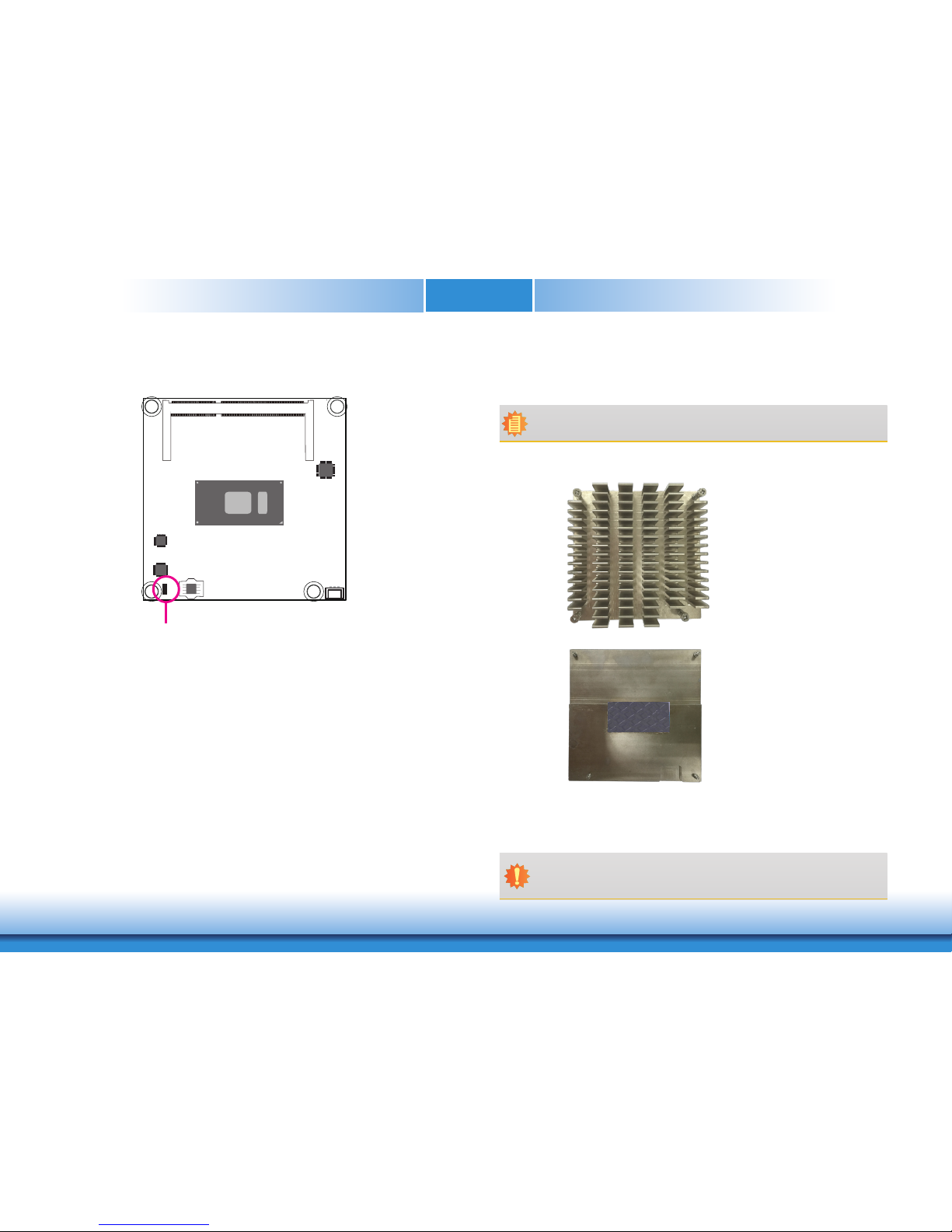
www.d.comChapter 3 Hardware Installation
22
Chapter 3
Standby Power LED
This LED will be lit when the system is in standby mode.
Standby
Power LED
Cooling Option
Heat Sink
• “1” denotes the location of the thermal pad designed to contact the corresponding
components that are on the SU968.
Top View of the Heat Sink
Important:
Remove the plastic covering from the thermal pads prior to mounting the heat sink
onto the SU968.
Note:
The system board used in the following illustrations may not resemble the actual
board. These illustrations are for reference only.
Bottom View of the Heat Sink
1
1
Page 23
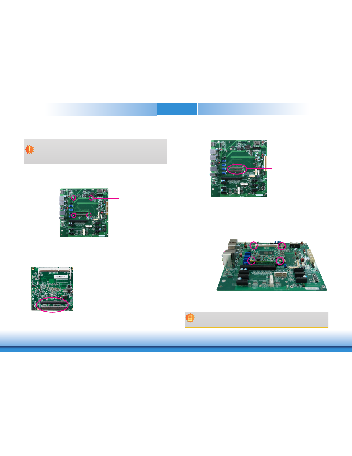
www.d.comChapter 3 Hardware Installation
23
Chapter 3
Installing SU968 onto a Carrier Board
Important:
The carrier board (COM332-B) and COM Express module used in this section are for
reference purpose only and may not resemble you carrier board and the acutal SU968
module. These illustrations are mainly to guide you on how to install SU968 onto the
carrier board of your choice.
1. Install the module and heat sink assembly onto the carrier board. The photo below shows
the location of the mounting holes on the carrier board.
COM Express connectors on the
carrier board
3. Press SU968 down firmly to seat it in the COM Express connectors of the carrier board.
Note:
The illustration above shows the pressing points of the module onto the carrier board.
Be careful when pressing the module to avoid damages to the connectors.
2. Grasp SU968 by its edges and position it on top of the carrier board with the mounting
holes of SU968 aligning with the standoffs on the carrier board. This will also align the
COM Express connectors of the two boards to each other.
Mounting standoffs
COM Express connectors on SU968
Pressing points
Page 24
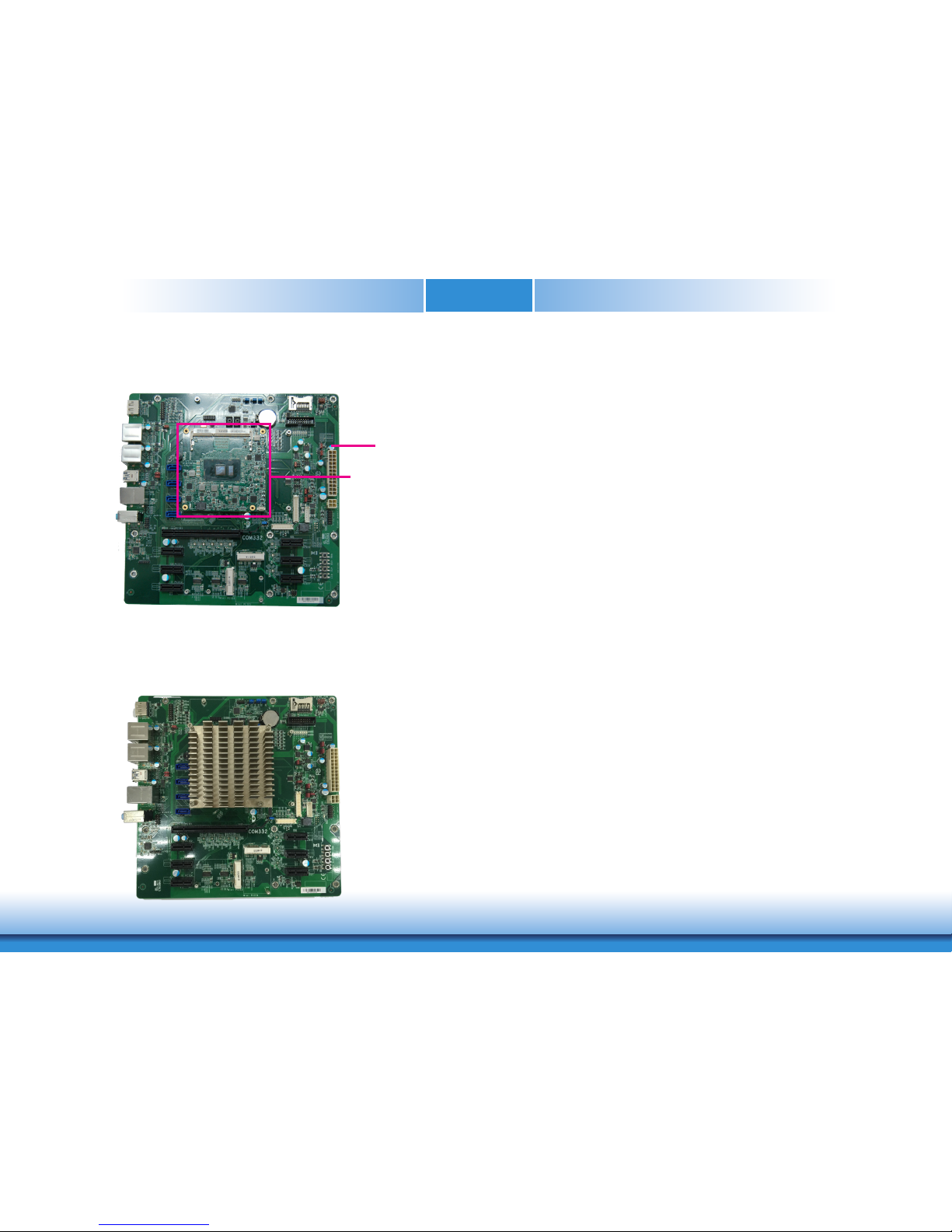
www.d.comChapter 3 Hardware Installation
24
Chapter 3
4. Verify that SU968 is firmly seated in the COM Express connectors of the carrier
board.
5. Install a heat sink onto the SU968 with the carrier board. The photo below shows the heat
sink installed on SU968.
Carrier board
SU968
Page 25
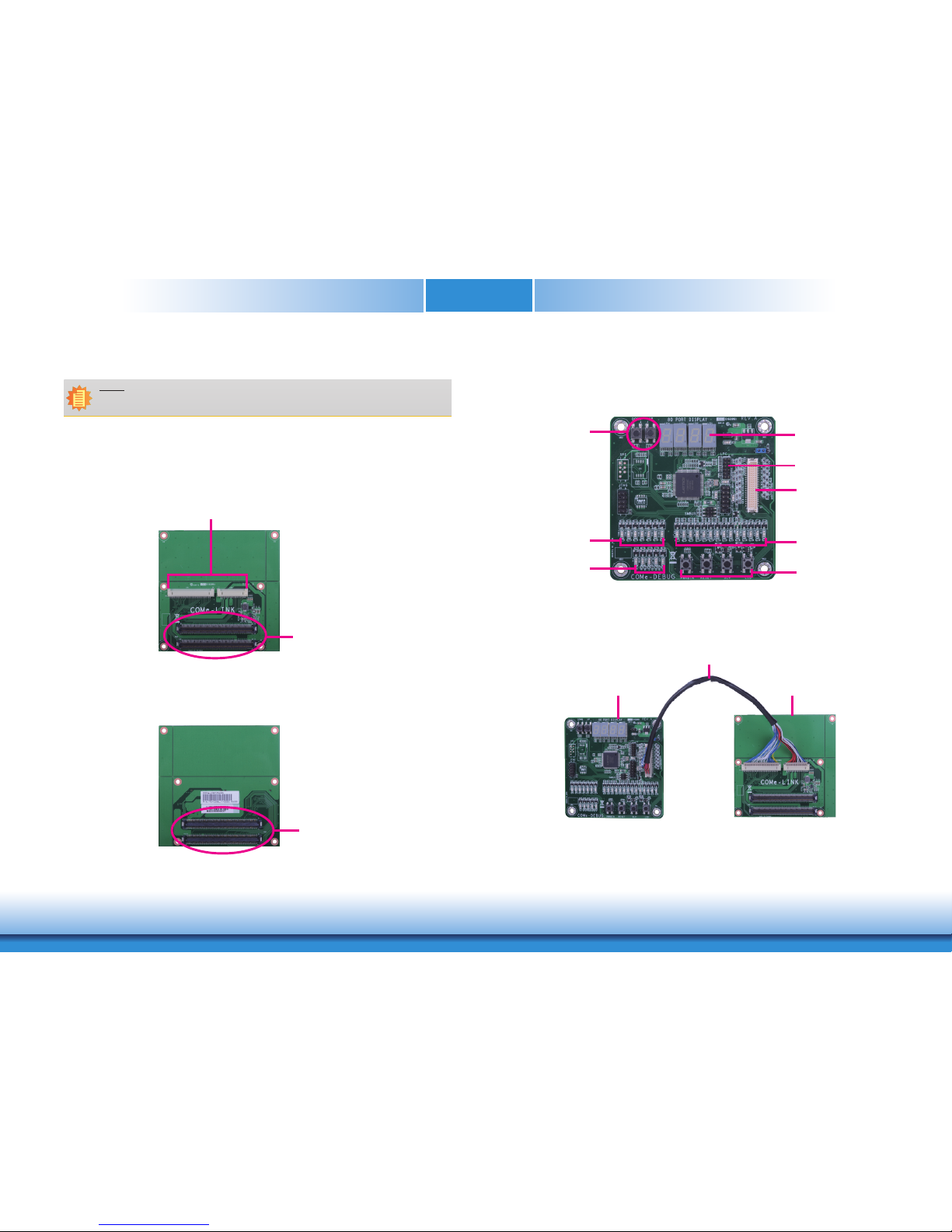
www.d.comChapter 3 Hardware Installation
25
Chapter 3
Installing the COM Express Debug Card
Note:
The system board used in the following illustrations may not resemble the actual
board. These illustrations are for reference only.
1. COMe-LINK1 is the COM Express debug card designed for COM Express Compact modules
to debug and display signals and codes of COM Express modules.
COMe-LINK1
Bottom view
Top view
COMe-DEBUG Connector
COM Express
Connectors
2. Connect the COMe-DEBUG card to COMe-LINK1 via a cable.
COMe-DEBUG COMe-LINK1
Cable
COMe-DEBUG
COM Express
Connectors
COMe-LINK1/2
Connector
Port 80 Display
LPC
COM Express
Signal Display
Power/Reset/
Sleep/LID control
COM Express
Type Display
Code Review
Control
COM Express
Power Display
Page 26
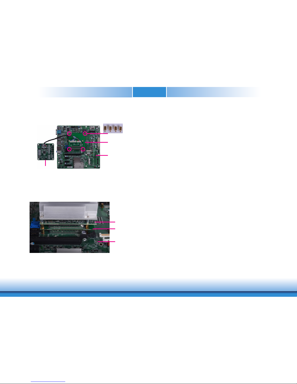
www.d.comChapter 3 Hardware Installation
26
Chapter 3
3. Use the provided screws to fix the COMe-LINK1 debug card onto the carrier board.
COMe-LINK1
Carrier Board
4. Then use the instructions from the previous section to install SU968 and heat sink on the
top of the COMe-LINK1 debug card.
Screws
COMe-DEBUG
Side View of the Module, Debug Card and Carrier Board
COMe-LINK1
Carrier Board
BW968
Page 27
www.d.comChapter 4 BIOS Setup
27
Chapter 4
Chapter 4 - BIOS Setup
KEYs Function
Right and Left Arrows Moves the highlight left or right to select a
menu.
Up and Down Arrows Moves the highlight up or down between
submenus or elds.
<Esc> Exits to the BIOS setup utility
<F1> Displays general help
<F5/F6> Changes the highlighted value
<F9> Changes to the default setup
<F10> Saves and exits the setup program.
<Enter> Press <Enter> to enter the highlighted
submenu
Scroll Bar
When a scroll bar appears to the right of the setup screen, it indicates that there are more
available fields not shown on the screen. Use the up and down arrow keys to scroll through all
the available fields.
Submenu
When ““ appears on the left of a particular field, it indicates that a submenu which contains
additional options are available for that field. To display the submenu, move the highlight to
that field and press <Enter>.
Legends
Overview
The BIOS is a program that takes care of the basic level of communication between the CPU
and peripherals. It contains codes for various advanced features found in this system board.
The BIOS allows you to configure the system and save the configuration in a battery-backed
CMOS so that the data retains even when the power is off. In general, the information stored
in the CMOS RAM of the EEPROM will stay unchanged unless a configuration change has been
made such as a hard drive replaced or a device added.
It is possible that the CMOS battery will fail causing CMOS data loss. If this happens, you need
to install a new CMOS battery and reconfigure the BIOS settings.
Default Configuration
Most of the configuration settings are either predefined according to the Load Optimal Defaults
settings which are stored in the BIOS or are automatically detected and configured without
requiring any actions. There are a few settings that you may need to change depending on
your system configuration.
Entering the BIOS Setup Utility
The BIOS Setup Utility can only be operated from the keyboard and all commands are keyboard commands. The commands are available at the right side of each setup screen.
The BIOS Setup Utility does not require an operating system to run. After you power up the
system, the BIOS message appears on the screen and the memory count begins. After the
memory test, the message “Press DEL to run setup” will appear on the screen. If the message
disappears before you respond, restart the system or press the “Reset” button. You may also
restart the system by pressing the <Ctrl> <Alt> and <Del> keys simultaneously.
Note:
The BIOS is constantly updated to improve the performance of the system board;
therefore the BIOS screens in this chapter may not appear the same as the actual
one. These screens are for reference purpose only.
Page 28
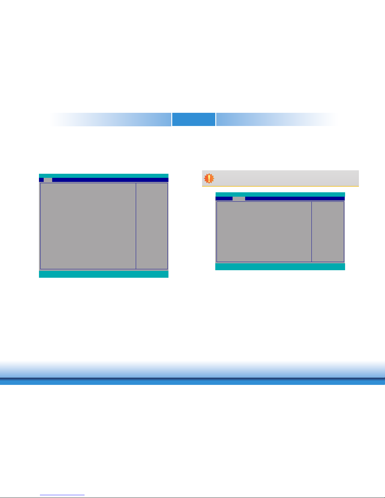
www.d.comChapter 4 BIOS Setup
28
Chapter 4
Main
The Main menu is the first screen that you will see when you enter the BIOS Setup Utility.
System Date
The date format is <month>, <date>, <year>. Month displays the month, from January to December. Date displays the date, from 1 to 31. Year displays the year, from
1980 to 2099.
System Time
The time format is <hour>, <minute>, <second>. The time is based on the 24-hour
military-time clock. For example, 1 p.m. is 13:00:00. Hour displays hours from 00 to
23. Minute displays minutes from 00 to 59. Second displays seconds from 00 to 59.
Insyde BIOS Setup Utility Advanced
The Advanced menu allows you to configure your system for basic operation. Some entries are
defaults required by the system board, while others, if enabled, will improve the performance
of your system or let you set some features according to your preference.
Important:
Setting incorrect field values may cause the system to malfunction.
This is the help for the
hour, minute, second
eld. Valid range is from
0 to 23, 0 to 59, 0 to 59.
INCREASE/REDUCE:
+/-.
InsydeH20 Setup Utility
Security
F1 Help ↑/↓ Select Item F5/F6 Change Values F9 Setup Defaults
Esc Exit ←/→ Select Item Enter Select SubMenu F10 Save and Exit
Project Name
BIOS Version
Processor Type
EC Ver:
CPUID:
CPU Speed:
CPU Stepping:
L1 Data Cache:
L1 Instruction Cache:
L2 Cache:
L3 Cache:
Number of Processors:
Microcode Rev:
Total Memory
System Memory Speed
SODIMM 0
SODIMM 1
PCH Rev / SKU
Intel ME Version / SKU
System Time
System Date
SU968
68.16A
Intel(R) Celeron (R) CPU 3599U @2.00 GHz
V1.2
0x406E3 (SKYLAKE ULT ULX)
2000 MHz
03 (D0/K0 Stepping)
32 KB
32 KB
256 KB
2048 KB
2 Core(s) / 2 Thread(s)
0000006A
4096 MB
1600 MHz
4096 MB
[Not Installed]
21 (C1 Stepping) / SKL PCH-LP (U) Premium
11.0.0. 1205 / CORPORATE
[05:18:30]
[05/14/2016]
Advanced Boot ExitMain
Rev. 5.0
ACPI Conguration Setting
ACPI Conguration
CPU Conguration
Video Conguration
Audio Conguration
SATA Conguration
USB Conguration
PCI Express Conguration
ME Conguration
MEBX Conguration
Active Management Technology Support
PC Health Status
Main Advanced
F1 Help ↑/↓ Select Item F5/F6 Change Values F9 Setup Defaults
Esc Exit ←/→ Select Item Enter Select SubMenu F10 Save and Exit
InsydeH20 Setup Utility
Security Boot Exit
Rev. 5.0
Page 29
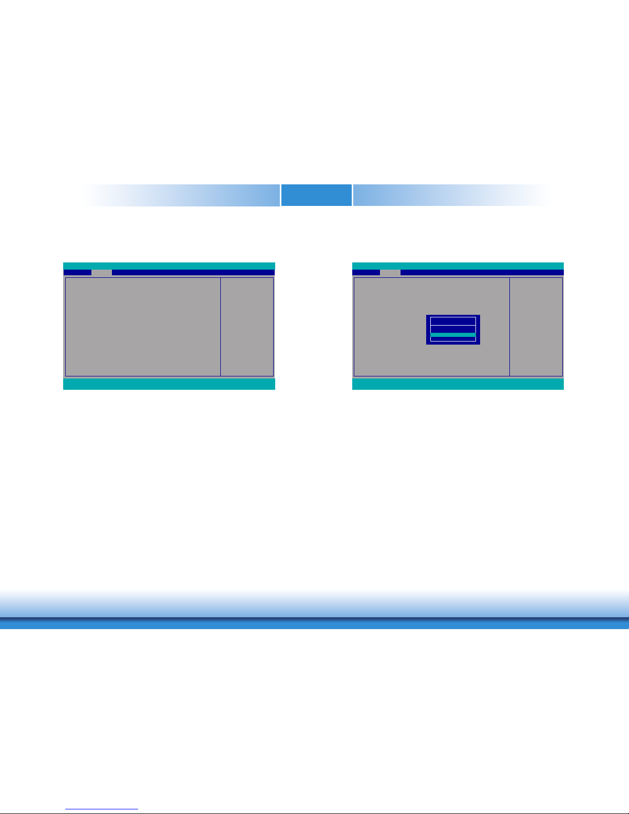
www.d.comChapter 4 BIOS Setup
29
Chapter 4
ACPI Settings
This section configures the ACPI settings.
Determines the action taken when the system power
is off and a PCI Power
Management Enable wake
up event occurs.
ACPI Conguration
Wake on LAN <Enabled>
After G3 <S0 State>
Advanced
F1 Help ↑/↓ Select Item F5/F6 Change Values F9 Setup Defaults
Esc Exit ←/→ Select Item Enter Select SubMenu F10 Save and Exit
InsydeH20 Setup Utility Rev. 5.0
Wake on LAN
Set this field to enable the system to be waken up via the onboard LAN or via a LAN
card that supports the remote wake up function.
State After G3
This field is to specify what state to go when power is re-applied after a power
failure (G3 state).
S0 State Power on the system when power is re-applied after AC power loss.
S5 State The system appears to be off when power is re-applied after AC power
loss.
CPU Configuration
This section configures the CPU.
Enable/Disable CPU Power
Management. Allows CPU
to go to C states when it’s
not 100% utilized.
CPU Conguration
Intel(R) SpeedStep(tm) <Enabled>
Turbo Mode <Enabled>
Advanced
F1 Help ↑/↓ Select Item F5/F6 Change Values F9 Setup Defaults
Esc Exit ←/→ Select Item Enter Select SubMenu F10 Save and Exit
InsydeH20 Setup Utility Rev. 5.0
Intel® SpeedStep™
This field is used to enable or disable the Enhanced Intel SpeedStep® Technology,
which helps optimize the balance between system’s power consumption and performance.
Turbo Mode
This field is used to enable or disable processor turbo mode (requires that EMTTM
is enabled too), which allows the processor core to automatically run faster than the
base frequency when the processor’s power, temperature, and specification are within
the limits of TDP.
Intel(R) SpeedStep(tm)
Disabled
Enabled
Page 30
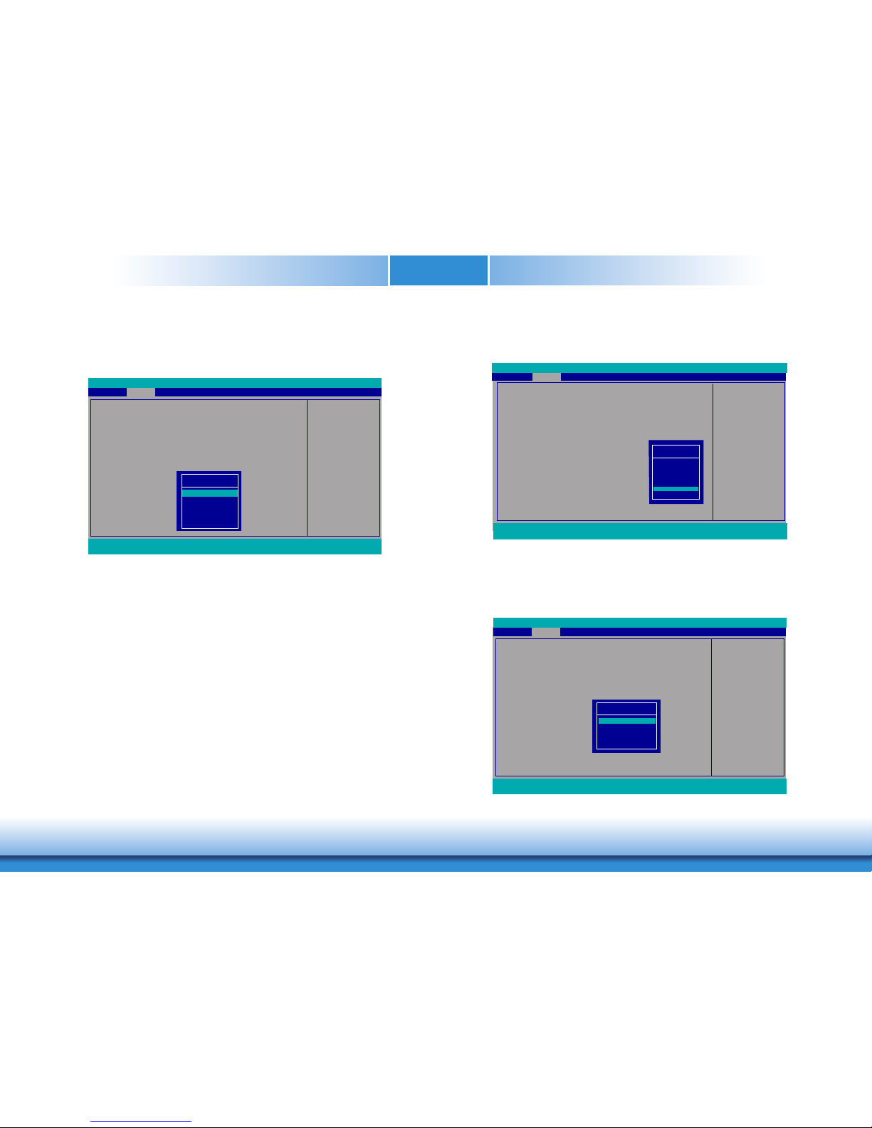
www.d.comChapter 4 BIOS Setup
30
Chapter 4
Video Configuration
This section configures the video settings.
Primary Display
Video Conguration
Internal Graphics
Always Enabled PEG
Boot display
Backlight Type
Panel Color Depth
LVDS Mode
LCD Panel Type
Advanced
F1 Help ↑/↓ Select Item F5/F6 Change Values F9 Setup Defaults
Esc Exit ←/→ Select Item Enter Select SubMenu F10 Save and Exit
InsydeH20 Setup Utility
<Auto>
<Disabled>
<DP1+VGA>
<Normal + PWM Mode>
<48 Bit>
<PWM Mode>
<1024x768>
<Auto>
<Disabled>
<DP1+VGA>
<Normal + PWM Mode>
<48 Bit>
<PWM Mode>
<1080x1024>
Backlight Type
Select the backlight type.
Internal Graphics
Auto
Disabled
Enabled
Keep IGFX enbled based
on the setup options.
Advanced
F1 Help ↑/↓ Select Item F5/F6 Change Values F9 Setup Defaults
Esc Exit ←/→ Select Item Enter Select SubMenu F10 Save and Exit
InsydeH20 Setup Utility
Boot display
LVDS + DP1
LVDS + VGA
VGA + DP1
DP1 + VGA
Choose display device
combination.
Boot display
Set the display device combination during system booting.
Rev. 5.0
Rev. 5.0
Internal Graphics
Keep IGFX enabled or disabled based on the setup options.
Always Enabled PEG
Enable or disable the PCIe graphics function.
Video Conguration
Internal Graphics
Always Enabled PEG
Boot display
Backlight Type
Panel Color Depth
LVDS Mode
LCD Panel Type
<Auto>
<Disabled>
<DP1+VGA>
<Normal + PWM Mode>
<48 Bit>
<PWM Mode>
<1280x1024>
Video Conguration
Internal Graphics
Always Enabled PEG
Boot display
Backlight Type
Panel Color Depth
LVDS Mode
LCD Panel Type
Advanced
F1 Help ↑/↓ Select Item F5/F6 Change Values F9 Setup Defaults
Esc Exit ←/→ Select Item Enter Select SubMenu F10 Save and Exit
InsydeH20 Setup Utility
<Auto>
<Disabled>
<DP1+VGA>
<Normal + PWM Mode>
<48 Bit>
<PWM Mode>
<1280x1024>
Backlight Type
Normal +PWM Mode
Normal +DC Mode
Invert +PWM Mode
Invert +DC Mode
Backlight Type Setting.
Rev. 5.0
Page 31
www.d.comChapter 4 BIOS Setup
31
Chapter 4
Audio Configuration
This section configures the audio settings.
HD Audio
Control the detection of the high-definition audio device.
Disabled
The high-definition audio will be unconditionally disabled.
Enabled
The high-definition audio will be unconditionally enabled.
Auto
The high-definition audio will be enabled if present and disabled otherwise.
HD Audio
Advanced
F1 Help ↑/↓ Select Item F5/F6 Change Values F9 Setup Defaults
Esc Exit ←/→ Select Item Enter Select SubMenu F10 Save and Exit
InsydeH20 Setup Utility
<Enabled>
Control Detection of the
HD-Audio device.
Disabled = HDA will be
unconditionally disabled
Enabled = HDA will be
unconditionally enabled
Auto = HDA will be enabled if present, disabled
otherwise.
Rev. 5.0
Advanced
F1 Help ↑/↓ Select Item F5/F6 Change Values F9 Setup Defaults
Esc Exit ←/→ Select Item Enter Select SubMenu F10 Save and Exit
InsydeH20 Setup Utility
LCD Panel Type
800x480
800x600
1024x768
1366x768
1280x1024
1920x1080
Select LCD Panel Type
Rev. 5.0
Video Conguration
Internal Graphics
Always Enabled PEG
Boot display
Backlight Type
Panel Color Depth
LVDS Mode
LCD Panel Type
<Auto>
<Disabled>
<DP1+VGA>
<Normal + PWM Mode>
<48 Bit>
<PWM Mode>
<1280x1024>
Panel Color Depth
Select the LFP panel color depth: 18 bit, 24 bit, 36 bit, and 48 bit.
LVDS Mode
Select PTN3460 (eDP to LVDS bridge IC) LVDS Mode: PWM Mode and DC Mode
LCD Panel Type
Select the LCD panel type.
Page 32
www.d.comChapter 4 BIOS Setup
32
Chapter 4
SATA Configuration
This section configures the SATA controller.
SATA Controller(s)
SATA Mode Selection
Serial ATA Port 0
Port 0
Serial ATA Port 1
Port 1
Serial ATA Port 2
Port 2
Serial ATA Port 3
Port 3
Advanced
F1 Help ↑/↓ Select Item F5/F6 Change Values F9 Setup Defaults
Esc Exit ←/→ Select Item Enter Select SubMenu F10 Save and Exit
<Enabled>
<AHCI>
[Not Installed]
<Enabled>
[Not Installed]
<Enabled>
[Not Installed]
<Enabled>
[Not Installed]
<Enabled>
Enable/Disable SATA
Device.
InsydeH20 Setup Utility Rev. 5.0
SATA Controller(s)
This field is used to enable or disable Serial ATA devices.
SATA Mode Selection
The mode selection configures the SATA controller(s).
AHCI Mode
This option allows the Serial ATA devices to use AHCI (Advanced Host Controller Interface).
RAID Mode
This option allows you to create RAID or Intel Matrix Storage configurations on Serial
ATA devices.
Serial ATA Port 0, 1, 2, and 3
This field is used to enable or disable each serial ATA port.
USB Configuration
This section configures the parameters of the USB devices.
USB BIOS Support
Disabled
Disable the USB keyboard/mouse/storage support.
Enabled
Enable the USB keyboard/mouse/storage support under UEFI and DOS environment.
Advanced
USB BIOS Support
F1 Help ↑/↓ Select Item F5/F6 Change Values F9 Setup Defaults
Esc Exit ←/→ Select Item Enter Select SubMenu F10 Save and Exit
InsydeH20 Setup Utility Rev. 5.0
<Enabled>
USB keyboard/mouse/storage support under UEFI
and DOS environment. It
will supporting UEFI en-
vironment only if set to
UEFI only
USB BIOS Support
Disabled
Enabled
Page 33
www.d.comChapter 4 BIOS Setup
33
Chapter 4
PCI Express Configuration
This section configures settings of PCI Express root ports.
PCI Express Root Port 1
PCI Express Root Port 2
PCI Express Root Port 3
PCI Express Root Port 4
PCI Express Root Port 6
PCI Express Root Port 9
PCI Express Root Port 10
PCI Express Root Port 11
Advanced
F1 Help ↑/↓ Select Item F5/F6 Change Values F9 Setup Defaults
Esc Exit ←/→ Select Item Enter Select SubMenu F10 Save and Exit
InsydeH20 Setup Utility Rev. 5.0
PCI Express Root Port 1
PCIe Speed
Advanced
F1 Help ↑/↓ Select Item F5/F6 Change Values F9 Setup Defaults
Esc Exit ←/→ Select Item Enter Select SubMenu F10 Save and Exit
<Enabled>
<AUTO>
InsydeH20 Setup Utility Rev. 5.0
PCI Express Root Ports
PCI Express Root Port 1
Settings.
Control the PCI Express
Root Port.
PCI Express Root Port
This field is used to enable or disable the PCI Express Root Port.
PCIe Speed
Select the speed of the PCI Express Root Port: Auto, Gen1, Gen2 or Gen3.
Active Management Technology Support
Intel AMT Support
Advanced
F1 Help ↑/↓ Select Item F5/F6 Change Values F9 Setup Defaults
Esc Exit ←/→ Select Item Enter Select SubMenu F10 Save and Exit
<Enabled>
Enable/Disable Intel (R)
Active Management Technology BIOS Extension.
Note : iAMT H/W is always enabled. This option
just controls the BIOS
extension execution.
InsydeH20 Setup Utility Rev. 5.0
Active Management Technology Support
The section allows users to enable or disable the Intel® Active Management Technology (Intel®
AMT) BIOS extension. Please refer to Chapter 7- Intel AMT Settings for more information.
Page 34
www.d.comChapter 4 BIOS Setup
34
Chapter 4
PC Health Status
This section configures the Embedded Controller (EC) settings.
COM Port 1
COM Port 2
WDT
PC Health Status
Advanced
F1 Help ↑/↓ Select Item F5/F6 Change Values F9 Setup Defaults
Esc Exit ←/→ Select Item Enter Select SubMenu F10 Save and Exit
InsydeH20 Setup Utility Rev. 5.0
<Enabled>
<Enabled>
<Disable>
Congure Serial port using
options: [Disable] No Configuration [Enable] User
Conguration
COM Port 1 and COM Port 2
Configure the settings of the serial ports.
Disable Disable the serial port.
Enable Enable the serial port.
COM Port 1
Disabled
Enabled
Enable/disable to flash
ME region
Me Fw Image Re-Flash
Advanced
F1 Help ↑/↓ Select Item F5/F6 Change Values F9 Setup Defaults
Esc Exit ←/→ Select Item Enter Select SubMenu F10 Save and Exit
<Disabled>
InsydeH20 Setup Utility Rev. 5.0
Me Fw Image Re-Flash
Disabled
Enabled
Un-congure ME without
password.
ME Configuration
This section configures flashing of Intel® Active Management Engine region.
Me Fw Image Re-Flash
Enable or disable flashing of the Intel® ME region.
Page 35
www.d.comChapter 4 BIOS Setup
35
Chapter 4
WDT
Enable or disable the watchdog function. A counter will appear if you select to enable
WDT. Input any value between 1 to 255 seconds.
COM Port 1
COM Port 2
WDT
COUNTER
PC Health Status
Advanced
F1 Help ↑/↓ Select Item F5/F6 Change Values F9 Setup Defaults
Esc Exit ←/→ Select Item Enter Select SubMenu F10 Save and Exit
<Auto>
<Auto>
<Enable>
[38]
The time-out counter rang-
es from 1 to 255 seconds
in the second mode.
PC Health Status
This screen displays PC health information.
PC Health Status
Voltage
VCORE
VBAT
1V35_DDR3
VccGT
VCCSA
Temperature
CPU (oC/oF)
Fan Speed
SYS FAN
CPU FAN
Advanced
F1 Help ↑/↓ Select Item F5/F6 Change Values F9 Setup Defaults
Esc Exit ←/→ Select Item Enter Select SubMenu F10 Save and Exit
0.923 V
3.278 V
1.275 V
0.011 V
0.988 V
82 C/ 179 F
0 RPM
4956 RPM
InsydeH20 Setup Utility Rev. 5.0
InsydeH20 Setup Utility Rev. 5.0
Security
This section configures the trusted platform module (TPM) and storage security.
TPM Availability
Show or hide the TPM availability and its configurations.
TPM Operation
Enable or disable the TPM function. It displays the following options:
• No Operation: No changes to the current state.
• Disable: Disable and deactivate TPM.
• Enable: Enable and activate TPM.
Clear TPM
Remove all TPM ownership contents.
When Hidden, don’t exposes TPM to 0
Current TPM Device
TPM State
TPM Availability
TPM Operation
Clear TPM
Supervisor Password
Set Supervisor Password
Set All Hdd Password
Set All Master Hdd Password
Storage Password Setup Page
Main Advanced
F1 Help ↑/↓ Select Item F5/F6 Change Values F9 Setup Defaults
Esc Exit ←/→ Select Item Enter Select SubMenu F10 Save and Exit
InsydeH20 Setup Utility
Security Boot Exit
Rev. 5.0
<TPM 1.2>
Enabled and Activated, Owned
<Available>
<No Operation>
[ ]
Not installed
TMP Availability
Available
Hidden
Page 36
www.d.comChapter 4 BIOS Setup
36
Chapter 4
Storage Password Setup Page
Enhance the HDD security by using a password.
Storage Password List
Help
Storage Password Setup
ST3160023AS
↑ and ↓ to change option, ENTER to select the option, ESC to exit
Main Advanced
F1 Help ↑/↓ Select Item F5/F6 Change Values F9 Setup Defaults
Esc Exit ←/→ Select Item Enter Select SubMenu F10 Save and Exit
InsydeH20 Setup Utility
Security Boot Exit
Rev. 5.0
Set Storage Password
Device Name:
Security Mode :
Set Storage Password
Set Master Hdd Password
Main Advanced
F1 Help ↑/↓ Select Item F5/F6 Change Values F9 Setup Defaults
Esc Exit ←/→ Select Item Enter Select SubMenu F10 Save and Exit
InsydeH20 Setup Utility
Security Boot Exit
Rev. 5.0
[ST3160023AS]
No Accessed
Set HDD password and suggest
the length of password greater
than one character.
Security Mode Description:
Lock: HDD security status is
enable and lock.
Unlock: HDD security status is
enable and unlock.
Change: HDD security status is
unlock and user changed to the
new password.
Disable: Remove HDD password
from device.
No Accessed: HDD security
status is not enabled when entering SCU.
How to clear HDD password:
only press “Enter” when set new
password.
Set Storage Password
Enter New Password:
Enter New Password Again:
Set Master HDD Password
Set a password for the master HDD.
Device Name:
Security Mode :
Set Storage Password
Set Master Hdd Password
Main Advanced
F1 Help ↑/↓ Select Item F5/F6 Change Values F9 Setup Defaults
Esc Exit ←/→ Select Item Enter Select SubMenu F10 Save and Exit
InsydeH20 Setup Utility
Security Boot Exit
Rev. 5.0
[ST3160023AS]
No Accessed
Set master HDD password and
suggest the length of password
greater than one character.
When security mode is lock,
input master HDD password to
unlock HDD.
Master HDD password is valid
when HDD password is set.
Only pressing “Enter would clear
HDD password and make HDD
security diable when set new
master HDD password.
Set Master Hdd Password
Enter New Password:
Enter New Password Again:
Set Master Hdd Password
Set master HDD password. The length of password must be greater than one character.
When the security mode is set to Lock, input the master HDD password to unlock the HDD.
Clear the HDD password by pressing “Enter” to set HDD security to be disabled
and set a new master HDD password.
Set all HDD password. The length of the password must be greater than one character.
Page 37
www.d.comChapter 4 BIOS Setup
37
Chapter 4
Set Supervisor Password
Set the administrative passwords. The length of the password must be greater than
one character.
Install or Change the password and the length of
password must be greater
than one character.
Current TPM Device
TPM State
TPM Availability
TPM Operation
Clear TPM
Supervisor Password
Set Supervisor Password
Main Advanced
F1 Help ↑/↓ Select Item F5/F6 Change Values F9 Setup Defaults
Esc Exit ←/→ Select Item Enter Select SubMenu F10 Save and Exit
InsydeH20 Setup Utility
Security Boot Exit
Rev. 5.0
<TPM 1.2>
Enabled and Activated, Owned
<Available>
<No Operation>
[X]
Not installed
Set Supervisor Password
Enter New Password:
Enter New Password Again:
Boot
This section configures boot options.
Numlock
Select the power-on state for numlock.
Boot Type
Select the boot type. The options include Dual Boot Type, Legacy Boot Type, and UEFI
Boot Type.
Network stack
Enable or disable UEFI network stack. It supports the operation of these functions or
software: Windows 8 BitLocker Network Unlock, UEFI IPv4/IPv6 PXE and legacy PXE
Option ROM.
USB Boot
Enable or disable the booting to USB boot devices.
Selects Power-on state for
Numlock
Numlock
Boot Type
Netwok Stack
PXE Boot capability
USB Boot
Main Advanced
F1 Help ↑/↓ Select Item F5/F6 Change Values F9 Setup Defaults
Esc Exit ←/→ Select Item Enter Select SubMenu F10 Save and Exit
InsydeH20 Setup Utility
Security Exit
Rev. 5.0
<On>
<Dual Boot Type>
<Disabled>
<Disabled>
<Enabled>
Boot
Note:
If the boot type is set to UEFI, the method for RAID volume creation will be
different. Please refer to Chapter 6 - RAID for more information.
Page 38
www.d.comChapter 4 BIOS Setup
38
Chapter 4
Normal Boot Menu
Normal
Select the boot menu type: normal or advanced.
For the advanced menu type: Use + and - keys to arrange the priority of the listed
boot devices.
For normal menu type: Select the "Boot Type Order" or "Hard Disk Drive" category to
view and arrange the order of the detected devices.
Main Advanced
F1 Help ↑/↓ Select Item F5/F6 Change Values F9 Setup Defaults
Esc Exit ←/→ Select Item Enter Select SubMenu F10 Save and Exit
InsydeH20 Setup Utility
Security Exit
Rev. 5.0
Boot
Boot Type Order
Hard Disk Drive
CD/DVD-ROM Drive
USB
Others
Floppy Drive
Boot Type Order
Main Advanced
F1 Help ↑/↓ Select Item F5/F6 Change Values F9 Setup Defaults
Esc Exit ←/→ Select Item Enter Select SubMenu F10 Save and Exit
InsydeH20 Setup Utility
Security ExitBoot
Hard Disk Drive
ST160LT007-9ZV14D
Hard Disk Drive
Rev. 5.0
Boot Type Order
Use + and - keys to arrange the sequence of storage devices that the system’s
hardware will check in the operating system’s boot files. The first device in the order
list has the first boot priority.
Hard Disk Drive
All installed hard disk drives will be displayed in this field. Use + and - keys to
arrange the sequence of hard disk drives that the system’s hardware will check in the
operating system’s boot files.
Legacy
This section configures legacy boot order.
Main Advanced
F1 Help ↑/↓ Select Item F5/F6 Change Values F9 Setup Defaults
Esc Exit ←/→ Select Item Enter Select SubMenu F10 Save and Exit
InsydeH20 Setup Utility
Security Exit
Rev. 5.0
Boot
Boot Device Priority
Normal Boot Menu
Boot Type Order
Hard Disk Drive
Select Normal Boot Option
Priority or Advance Boot
Option Priority
<Normal>
Normal Boot Menu
Normal
Advance
Page 39
www.d.comChapter 4 BIOS Setup
39
Chapter 4
Exit
This section configures the parameters for exiting the BIOS menu.
Exit Saving Changes
Select this field and then press <Enter> to exit the BIOS setup and save your
changes.
Load Optimal Defaults
Select this field and then press <Enter> to load optimal defaults.
Discard Changes
Select this field and then press <Enter> to exit the BIOS setup without saving your
changes.
Exit system setup and save
your changes.
Exit Saving Changes
Load Optimal Defaults
Discard Changes
Main Advanced
F1 Help ↑/↓ Select Item F5/F6 Change Values F9 Setup Defaults
Esc Exit ←/→ Select Item Enter Select SubMenu F10 Save and Exit
InsydeH20 Setup Utility
Security Boot
Rev. 5.0
Exit
CD/DVD-ROM Drive
All installed CD/DVD-ROM drives will be displayed in this field. Use + and - keys to arrange
the sequence of CD/DVD-ROM drives that the system’s hardware checks for the operating system’s boot files.
Main Advanced
F1 Help ↑/↓ Select Item F5/F6 Change Values F9 Setup Defaults
Esc Exit ←/→ Select Item Enter Select SubMenu F10 Save and Exit
InsydeH20 Setup Utility
Security ExitBoot
CD/DVD-ROM Drive
ATAP1 iHAS324 Y
CD/DVD-ROM Drive
Rev. 5.0
Page 40
www.d.comChapter 4 BIOS Setup
40
Chapter 4
R
Read le successfully. (path= “platform.ini”)
Insyde H20FFT (Flash Firmware Tool) Version (SEG) 100.00.08.10
Copyright(c) 2012 - 2016, Insyde Software Corp. All Rights Reserved.
Initializing
Current BIOS Model name: SU968
New BIOS Model name: SU968
Current BIOS version: 65.05A
New BIOS version: 65.05A
Updating Block at FFFFF000h
0% 25% 50% 75% 100%
100%
C:\SU968>_
Notice: BIOS SPI ROM
1. The Intel® Management Engine has already been integrated into this system board. Due to
the safety concerns, the BIOS (SPI ROM) chip cannot be removed from this system board
and used on another system board of the same model.
2. The BIOS (SPI ROM) on this system board must be the original equipment from the factory
and cannot be used to replace one which has been utilized on other system boards.
3. If you do not follow the methods above, the Intel® Management Engine will not be
updated and will cease to be effective.
Note:
a. You can take advantage of flash tools to update the default configuration of the
BIOS (SPI ROM) to the latest version anytime.
b. When the BIOS IC needs to be replaced, you have to populate it properly onto the
system board after the EEPROM programmer has been burned and follow the
technical person's instructions to confirm that the MAC address should be burned
or not.
Updating the BIOS
To update the BIOS, you will need the new BIOS file and a flash utility. Please contact technical support or your sales representative for the files and specific instructions about how to
update BIOS with the flash utility.
When you download the given BIOS file, you may find a BIOS flash utility attached with the
BIOS file. This is the utility for performing BIOS updating procedure. For your convenience, we
will also provide you with an auto-execution file in the BIOS file downloaded. This auto-execution file will bring you directly to the flash utility menu soon after system boots up and finishes
running the boot files in your boot disk.
Information
Please do not remove the AC power
Page 41
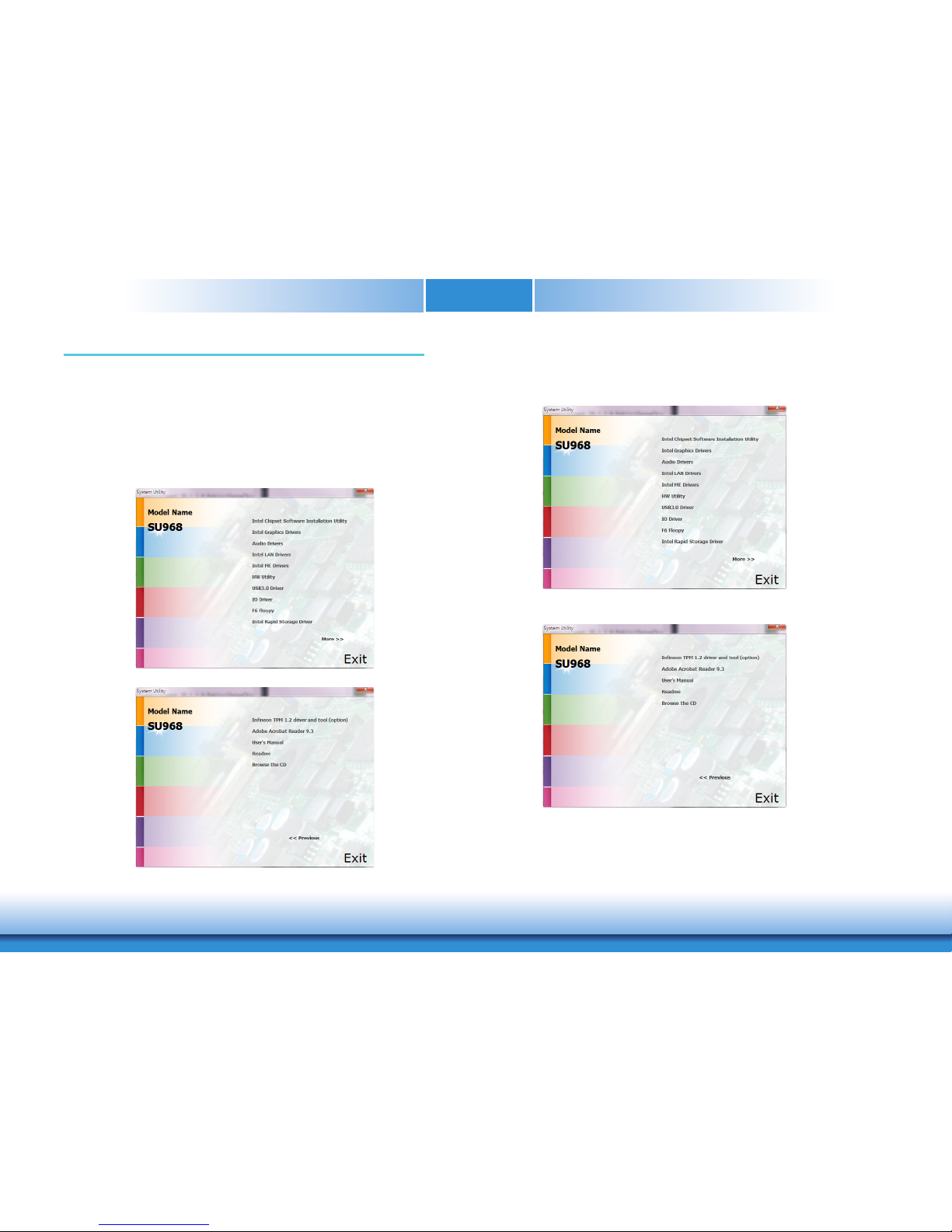
www.d.comChapter 5 Supported Software
41
Chapter 5
Chapter 5 - Supported Software
The DVD that came with the system board contains drivers, utilities and software applications
required to enhance the performance of the system board.
Insert the DVD into a DVD-ROM drive. The autorun screen (Mainboard Utility DVD) will appear.
If after inserting the DVD, “Autorun” did not automatically start (which is, the Mainboard Utility
DVD screen did not appear), please go directly to the root directory of the DVD and doubleclick “Setup”.
Auto Run Page (For Windows 10)
Auto Run Page (For Windows 8.1)
Page 42
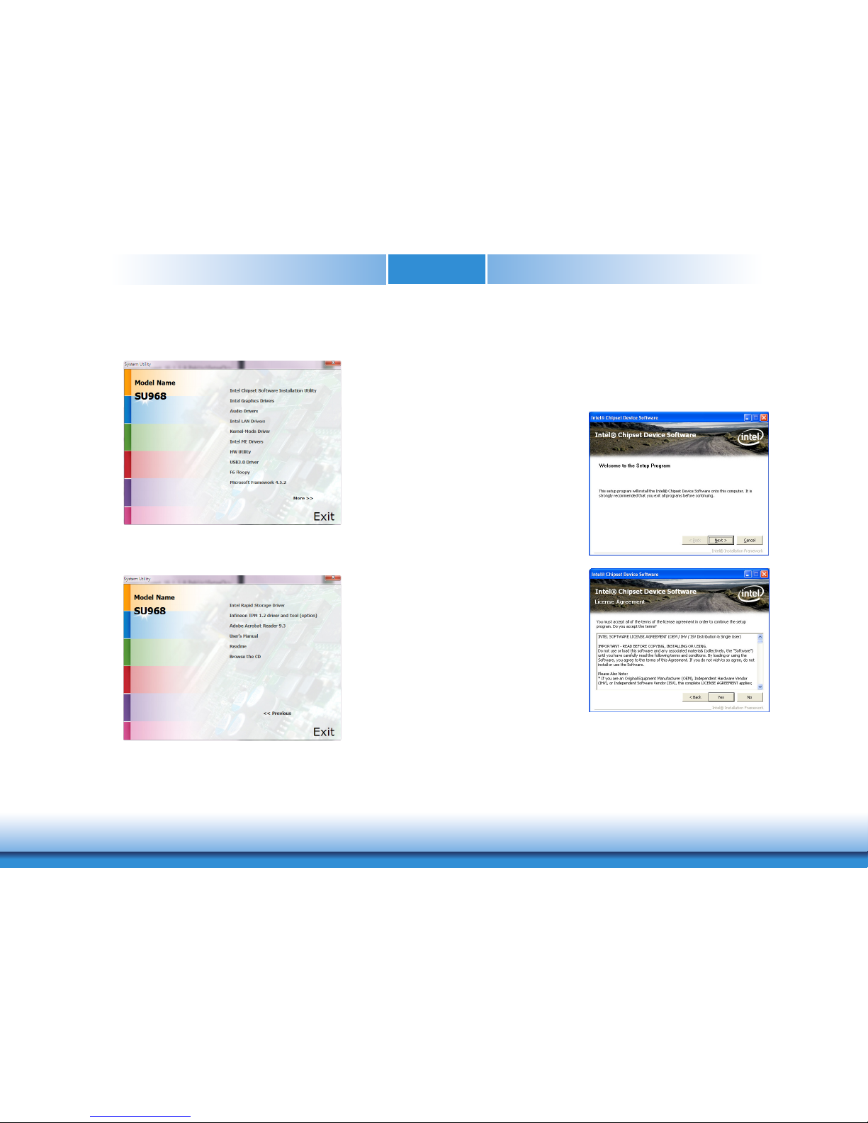
www.d.comChapter 5 Supported Software
42
Chapter 5
Auto Run Page (For Windows 7) Intel Chipset Software Installation Utility
The Intel Chipset Software Installatn Utility is used for updating Windows® INF files so that the
Intel chipset can be recognized and configured properly in the system.
To install the utility, click “Intel Chipset Software Installation Utility” on the main menu.
1. Setup is ready to install the
utility. Click “Next”.
2. Read the license agreement
then click “Yes”.
Page 43
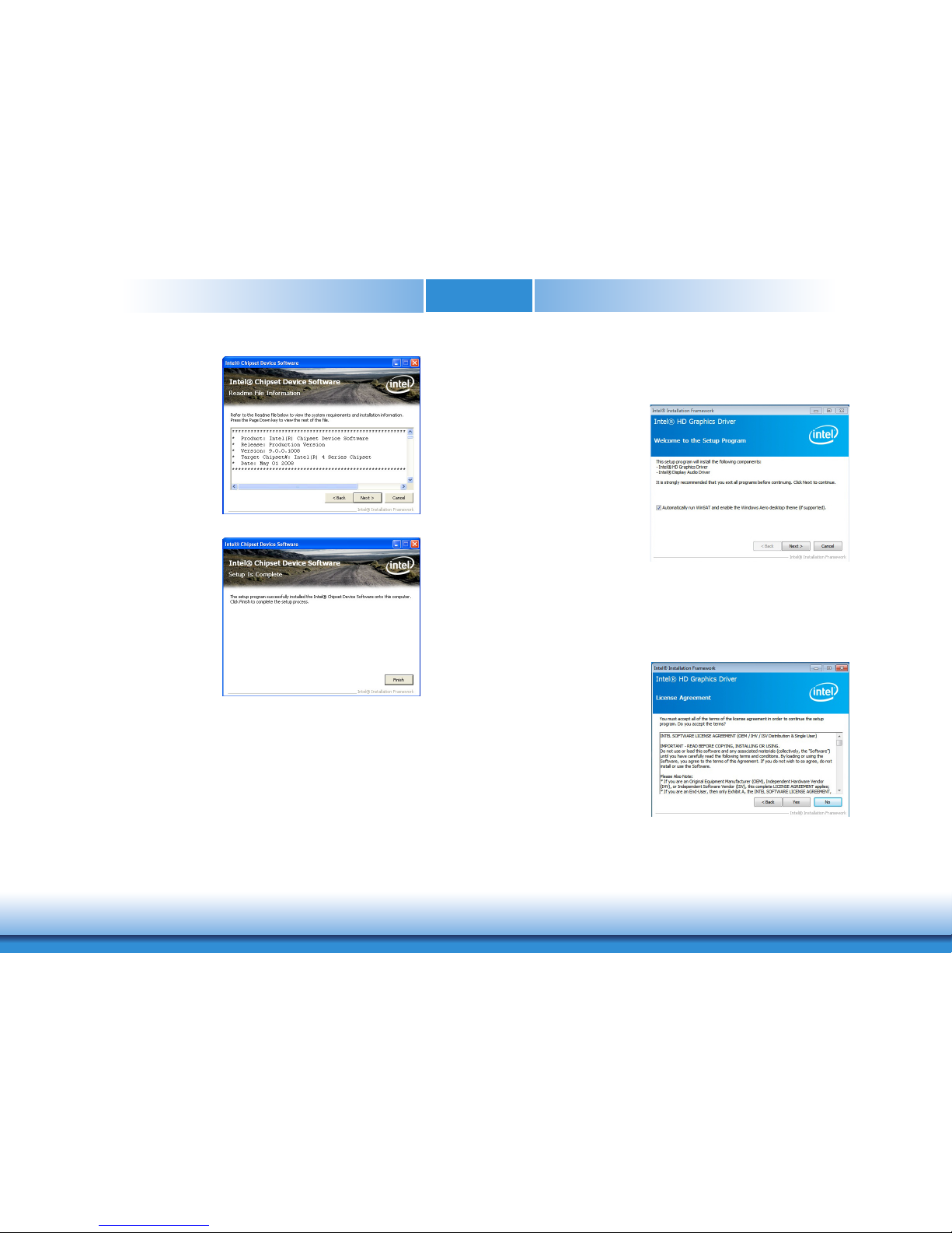
www.d.comChapter 5 Supported Software
43
Chapter 5
3. Go through the readme
document for more installation tips then click “Next”.
4. After completing installation, click “Finish” to exit
setup.
Intel Graphics Drivers
To install the driver, click “Intel Graphics Drivers” on the main menu.
1. Setup is now ready to
install the graphics driver.
Click “Next”.
2. Read the license agreement
then click “Yes”.
By default, the “Automatically run WinSAT and enable the Windows Aero desktop theme” is
enabled. With this enabled, after installing the graphics driver and the system rebooted, the
screen will turn blank for 1 to 2 minutes (while WinSAT is running) before the Windows 7/
Windows 8.1/ Windows 10 desktop appears. The “blank screen” period is the time Windows is
testing the graphics performance.
We recommend that you skip this process by disabling this function then click “Next”.
Page 44
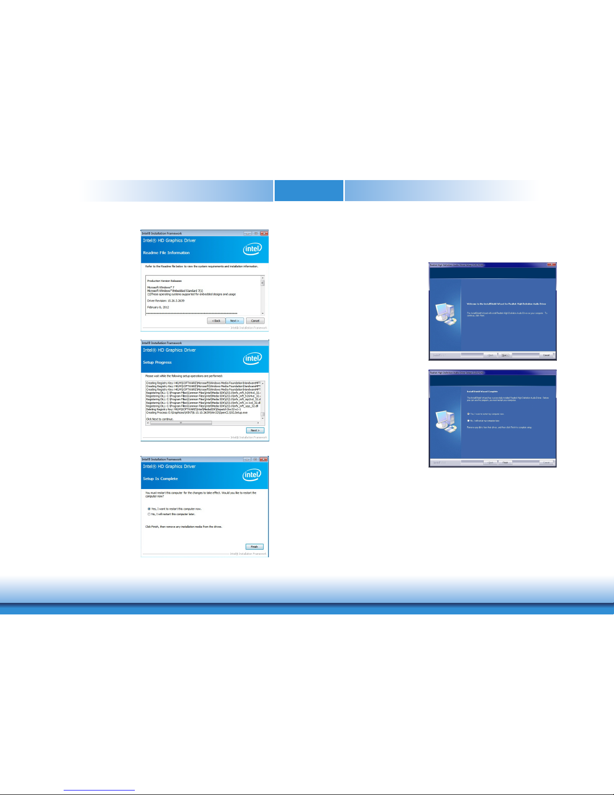
www.d.comChapter 5 Supported Software
44
Chapter 5
4. Setup is now installing
the driver. Click “Next” to
continue.
3. Go through the readme
document for system requirements and installation
tips then click “Next”.
5. Click “Yes, I want to restart
this computer now” then
click “Finish”.
Restarting the system will
allow the new software
installation to take effect.
1. Setup is now ready to install the
audio driver. Click “Next”.
2. Follow the remainder of the steps
on the screen; clicking “Next”
each time you finish a step.
3. Click “Yes, I want to restart my
computer now” then click “Finish”.
Restarting the system will allow the
new software installation to take
effect.
Audio Drivers (For COM332-B Carrier Board)
To install the driver, click “Audio Drivers (for COM332-B Carrier Board)” on the main menu.
Page 45
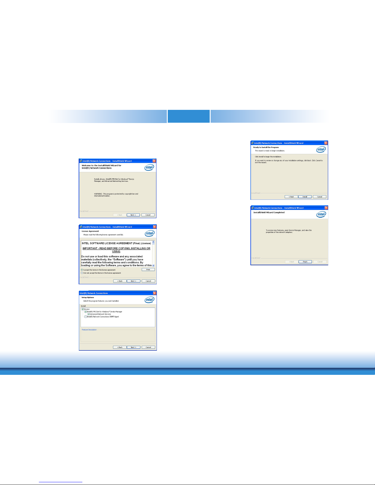
www.d.comChapter 5 Supported Software
45
Chapter 5
Intel LAN Drivers
To install the driver, click “Intel LAN Drivers” on the main menu.
1. Setup is ready to install the
driver. Click “Next”.
2. Click “I accept the terms
in the license agreement”
then click “Next”.
3. Select the program featuers
you want installed then
click “Next”.
4. Click “Install” to begin the
installation.
5. After completing installation, click “Finish”.
Page 46
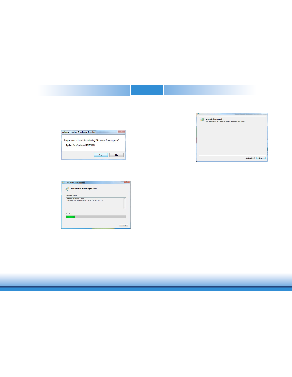
www.d.comChapter 5 Supported Software
46
Chapter 5
Kernel Mode Driver (For Windows 7 only)
To install the driver, click “Kernel Mode Driver Framework” on the main menu.
1. Click “Yes“ to install the
update.
2. The update is installed
now.
3. Click “Restart Now“ to
restart your computer when
the installation is complete.
Page 47
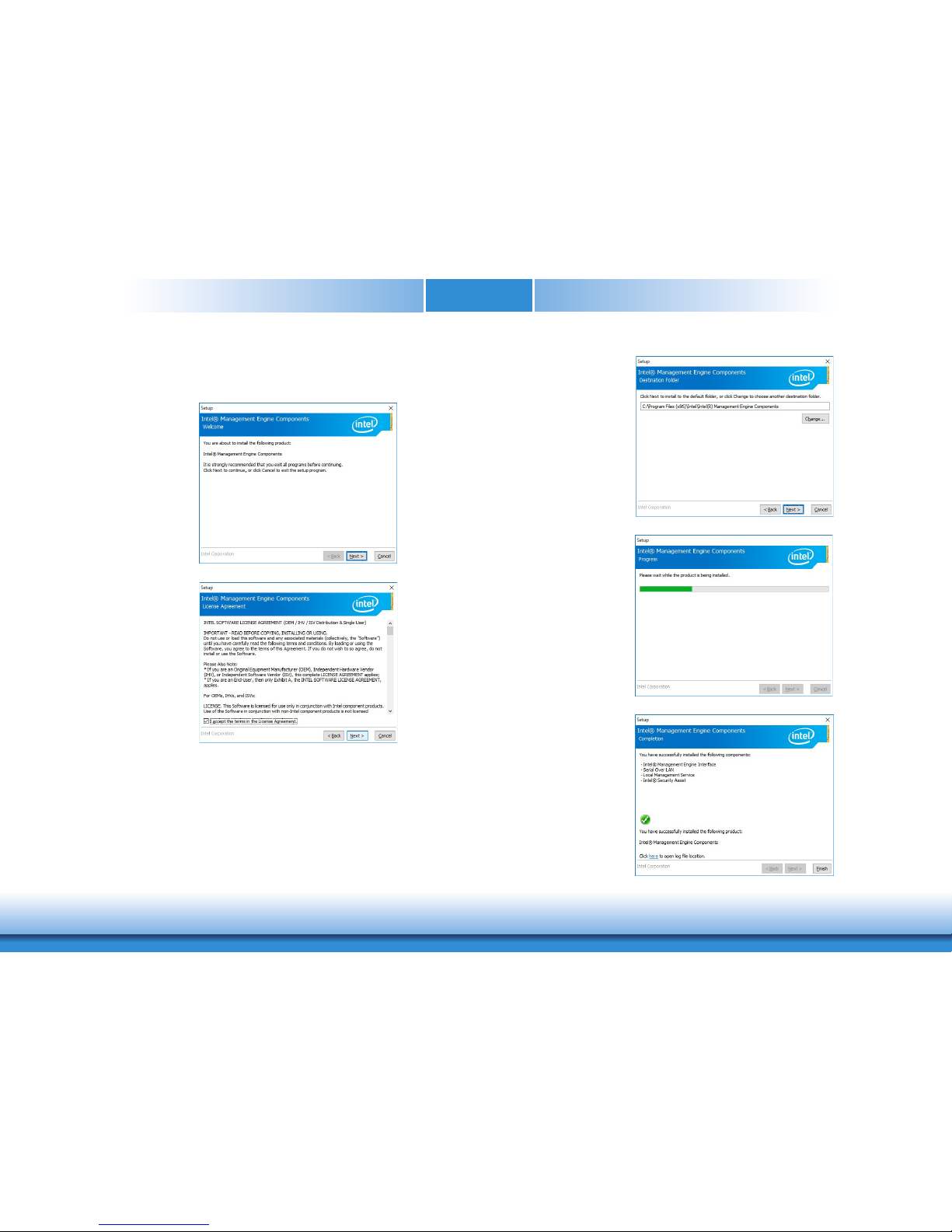
www.d.comChapter 5 Supported Software
47
Chapter 5
Intel Management Engine Drivers
To install the driver, click “Intel Management Engine Drivers” on the main menu.
1. Setup is ready to install the
driver. Click “Next”.
2. Read the license agreement
then click “Next”.
3. Setup is currently installing
the driver. After installation
has completed, click “Next”.
4. Please wait while the product is being installed.
5. After completing installation, click “Finish”.
Page 48
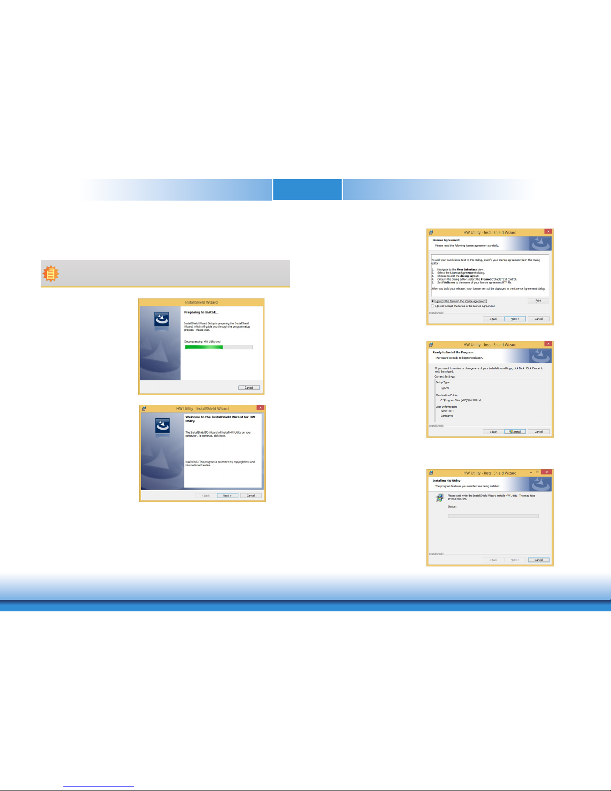
www.d.comChapter 5 Supported Software
48
Chapter 5
HW Utility
HW Utility provides information about the board, Watchdog, and DIO. To access the utility,
click “HW Utility” on the main menu.
Note:
If you are using Windows 7 or later versions, you need to access the operating system
as an administrator to be able to install the utility.
1. Setup is ready to install the
driver.
2. Click “Next” to continue.
3. Read the license agreement
then click “I accept the terms
in the license agreement”.
Click “Next”.
4. The wizard is ready to begin
installation. Click “Install”.
5. Please wait while the program
features are being installed.
Page 49
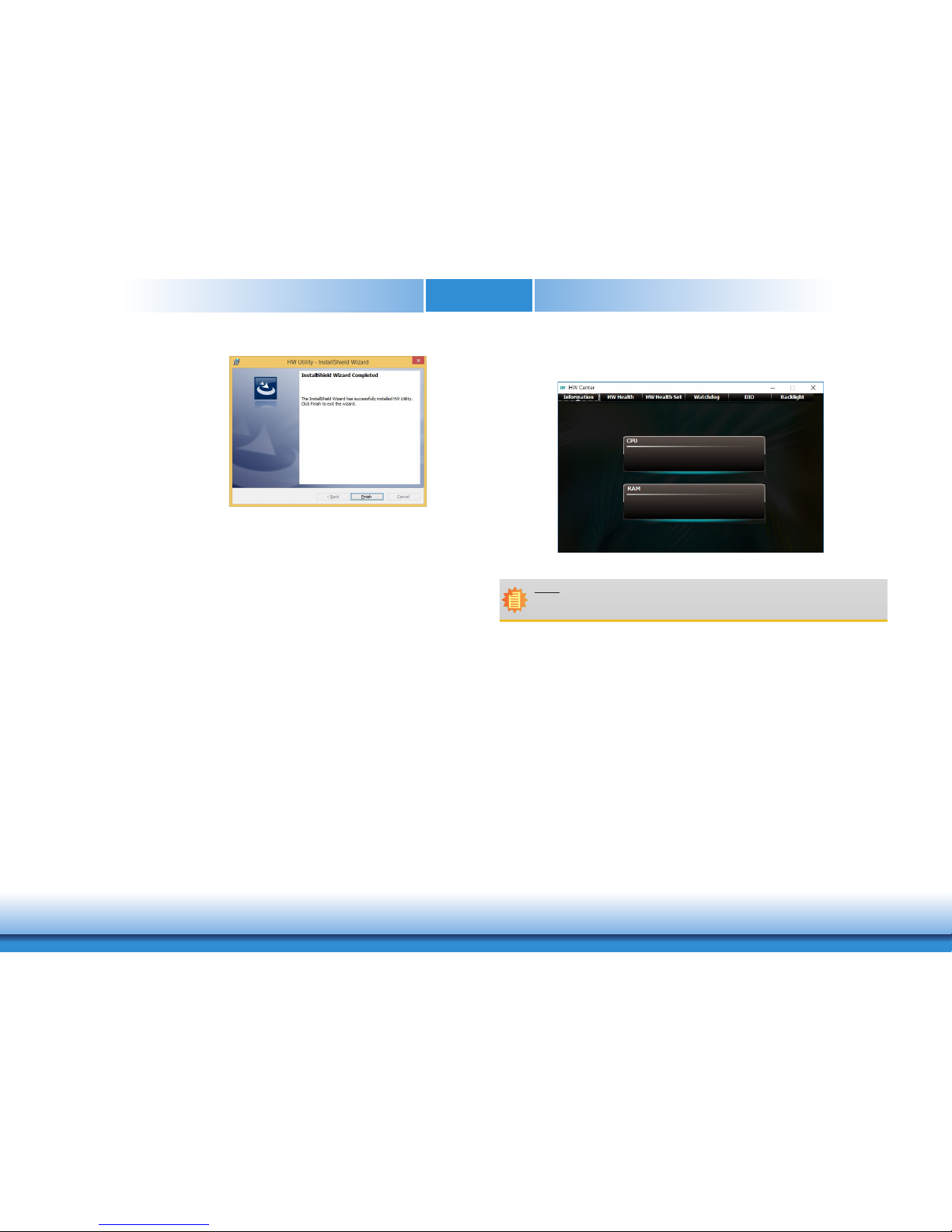
www.d.comChapter 5 Supported Software
49
Chapter 5
6. After completing installation, click “Finish”.
The HW Utility icon will appear on the desktop. Double-click the icon to open the utility.
SU968
Note:
Note: The screenshot displayed above is for illustrative purpose only, and may not
resemble the actual screen.
The SU968 HW Utility features the following tabs: Information, HW Health, HW Healthset,
Watchdog, DIO and Backlight. Click on the tabs to access information about the board.
Page 50
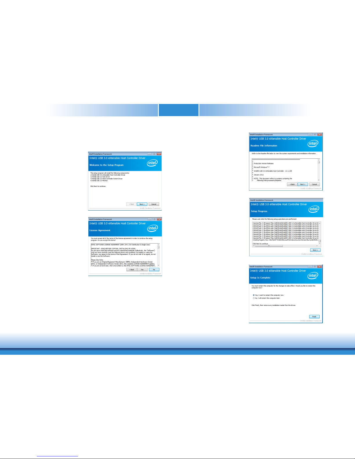
www.d.comChapter 5 Supported Software
50
Chapter 5
Intel USB 3.0 Drivers
To install the driver, click “Intel USB 3.0 Driver” on the main menu.
2. Read the license agreement then
click “Yes”.
1. Setup is ready to install the driver.
Click “Next”.
3. Go through the readme document for more installation tips
then click “Next”.
4. Setup is currently installing the
driver. After installation has completed, click “Next”.
5. After completing installation, click
“Finish”.
Page 51
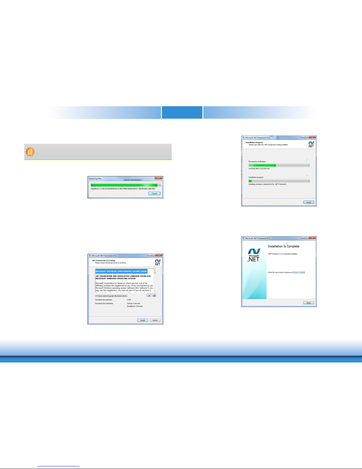
www.d.comChapter 5 Supported Software
51
Chapter 5
Microsoft Framework 4.5.2 (For Windows 7)
To install the driver, click “Microsoft Framework 4.5.2” on the main menu.
1. Setup is now extracting files.
Note:
Before installing Microsoft Framework 4.5.2, make sure you have updated your
Windows 7 operating system to Service Pack 1.
2. Read the license agreement carefully.
Click “I have read and accept
the terms of the License Agree
ment” then click “Install”.
4. Click “Finish”.
3. Setup is now installing the
driver.
Page 52
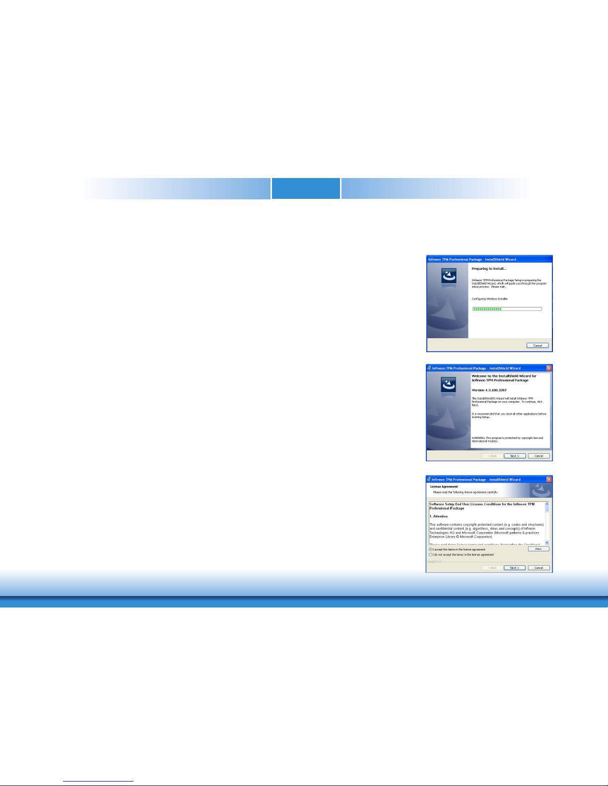
www.d.comChapter 5 Supported Software
52
Chapter 5
Intel Rapid Storage Technology
The Intel Rapid Storage Technology is a utility that allows you to monitor the current status
of the SATA drives. It enables enhanced performance and power management for the storage
subsystem.
To install the driver, click “Intel Rapid Storage Technology” on the main menu. Please refer to
Chapter 6 for more information.
Infineon TPM 1.2 Driver and Tool (Optional)
To install the driver, click “Infineon TPM driver and tool (option)” on the main menu.
1. The setup program is preparing
to install the driver.
2. The setup program is now ready
to install the utility. Click “Next”.
3. Click “I accept the terms in the
license agreement” and then
click “Next”.
Page 53
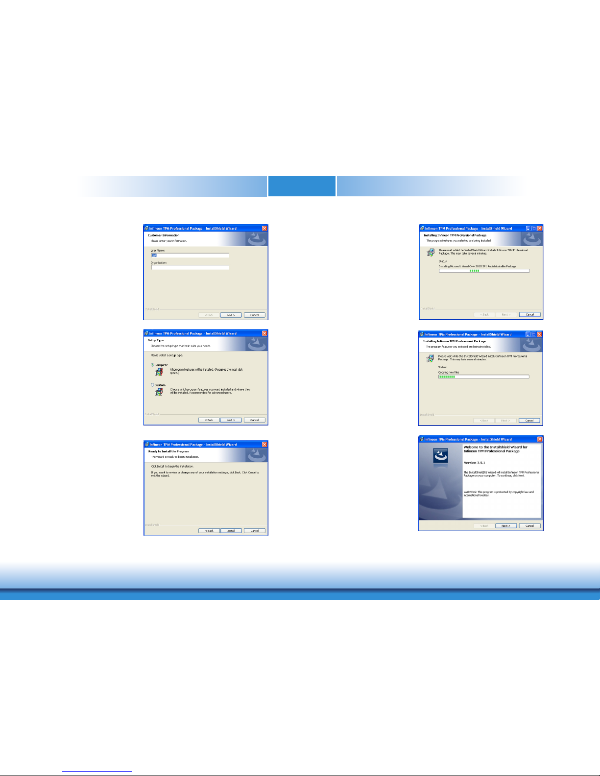
www.d.comChapter 5 Supported Software
53
Chapter 5
4. Enter the necessary information
and then click “Next”.
5. Select a setup type and then click
“Next”.
6. Click “Install”.
7. TPM requires installing the Microsoft Visual C++ package prior to
installing the utility. Click “Install”.
8. The setup program is currently
installing the Microsoft Visual
C++ package.
9. Click “Finish”.
Page 54
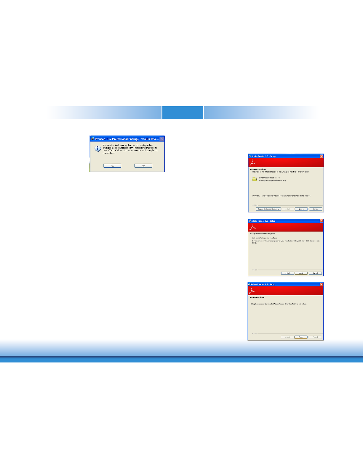
www.d.comChapter 5 Supported Software
54
Chapter 5
10. Click “Yes” to restart your system.
Adobe Acrobat Reader 9.3
To install the reader, click “Adobe Acrobat Reader 9.3” on the main menu.
1. Click Next to install or click
Change Destination Folder
to select another folder.
2. Click “Install” to begin instal-
lation.
3. Click “Finish” to exit installation.
Page 55
www.d.comChapter 6 RAID
55
Chapter 6
Chapter 6 - RAID
The system board allows configuring RAID on Serial ATA drives. It supports RAID 0, RAID 1,
RAID 5 and RAID 10.
RAID Levels
RAID 0 (Striped Disk Array without Fault Tolerance)
RAID 0 uses two new identical hard disk drives to read and write data in parallel, interleaved
stacks. Data is divided into stripes and each stripe is written alternately between two disk
drives. This improves the I/O performance of the drives at different channel; however it is not
fault tolerant. A failed disk will result in data loss in the disk array.
RAID 1 (Mirroring Disk Array with Fault Tolerance)
RAID 1 copies and maintains an identical image of the data from one drive to the other drive.
If a drive fails to function, the disk array management software directs all applications to the
other drive since it contains a complete copy of the drive’s data. This enhances data protection
and increases fault tolerance to the entire system. Use two new drives or an existing drive and
a new drive but the size of the new drive must be the same or larger than the existing drive.
RAID 5
RAID 5 stripes data and parity information across hard drives. It is fault tolerant and provides
better hard drive performance and more storage capacity.
RAID 10 (Mirroring and Striping)
RAID 10 is a combination of data striping and data mirroring providing the benefits of both
RAID 0 and RAID 1. Use four new drives or an existing drive and three new drives for this
configuration.
RAID Level Min. Drives Protection Description
RAID 0 2 None Data striping without redundancy
RAID 1 2 Single Drive Failure Disk mirroring
RAID 5 3 Single Drive Failure
Block-level data striping with
distributed parity
RAID 10 4
1 Disk Per Mirrored
Stripe (not same mirror)
Combination of RAID 0 (data striping)
and RAID 1 (mirroring)
Settings
To enable the RAID function, the following settings are required.
1. Connect the Serial ATA drives.
2. Enable Serial ATA in the Insyde BIOS.
3. Create a RAID volume.
4. Install the Intel Rapid Storage Technology Utility.
Step 1: Connect the Serial ATA Drives
Refer to Chapter 2 for details on connecting the Serial ATA drives.
Important:
1. Make sure you have installed the Serial ATA drives and connected the data cables
otherwise you won’t be able to enter the RAID BIOS utility.
2. Treat the cables with extreme caution especially while creating RAID. A damaged
cable will ruin the entire installation process and operating system. The system will
not boot and you will lost all data in the hard drives. Please give special attention
to this warning because there is no way of recovering back the data.
Step 2: Enable RAID in the Insyde BIOS
1. Power-on the system then press <Del> to enter the main menu of the Insyde BIOS.
2. Go to “Advanced” menu, and select the “SATA Configuration” menu.
3. Change the “SATA Mode Selection” to “RAID” mode.
4. Save the changes in the “Save & Exit” menu.
5. Reboot the system.
Page 56
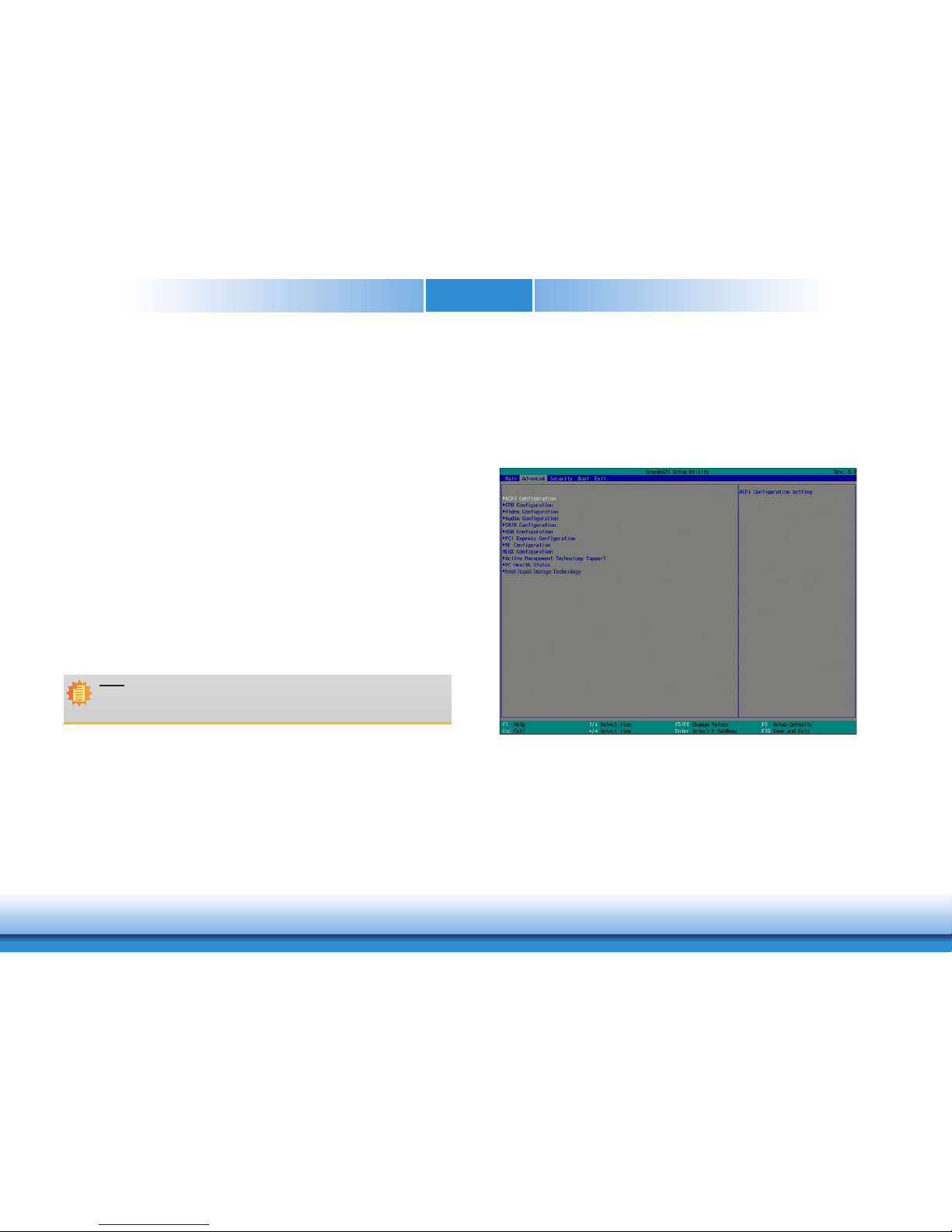
www.d.comChapter 6 RAID
56
Chapter 6
Step 3: Create a RAID Volume
1. When the Intel® RST option ROM status screen displays during POST, press <Ctrl> and
<I> simultaneously to enter the option ROM user interface.
2. Select 1: Create RAID Volume and press <Enter>.
3. Use the up or down arrow keys to select the RAID level and press <Enter>.
4. Use the up or down arrow keys to select the strip size and press <Enter>.
5. Press <Enter> to select the physical disks.
6. Use the up or down arrow keys to scroll through the list of hard drives and press <Space>
to select the drive.
7. Press <Enter>.
8. Select the volume size and press <Enter>. You must select less than one hundred percent
of the available volume space to leave space for the second volume.
9. Press <Enter> to create the volume.
10. At the prompt, press <Y> to confirm volume creation.
11. Select 4: Exit and press <Enter>.
12. Press <Y> to confirm exit.
Note:
These steps are cited from the Intel® Suppot site, “Set Up a System with Intel®
Matrix RAID Technology” (Article ID: 000005789).
http://www.intel.com/content/www/us/en/support/boards-and-kits/000005789.htm
Step 3-1: Create a RAID Volume if the boot type is UEFI
If the boot type is set to UEFI, RAID volume creation will be different. Please use the following
steps to create RAID volumes. To set the boot type, enter the Insyde BIOS and go to “Boot”
>”Boot type”.
1. Go to the “Advanced” menu of the Insyde BIOS.
2. The “Intel® Rapid Storage Technology” menu appears. Enter this menu.
3. The screen displays all available drives. Select “Create RAID volume” to create a RAID
volume”.
4. Use the up or down arrow keys to select the RAID level and press <Enter>.
5. Use the up or down arrow keys to scroll through the list of hard drives and press <Space>
to select the drive.
6. Press <Enter>.
7. Use the up or down arrow keys to select the strip size and press <Enter>.
8. Enter the volume size and press <Enter>.
9. At the prompt, press <Y> to confirm volume creation.
Page 57
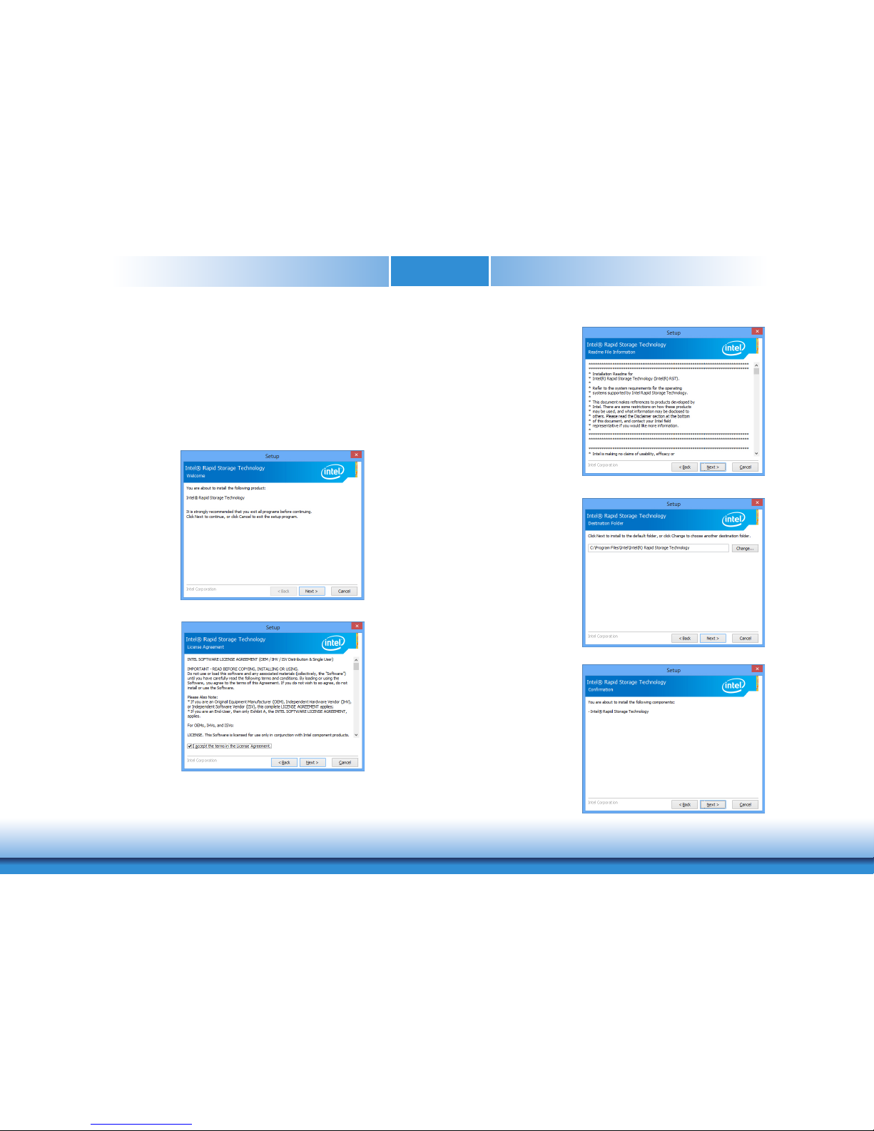
www.d.comChapter 6 RAID
57
Chapter 6
Step 4: Install the Intel Rapid Storage Technology Utility
The Intel Rapid Storage Technology Utility can be installed from within Windows. It allows
RAID volume management (create, delete, migrate) from within the operating system. It will
also display useful SATA device and RAID volume information. The user interface, tray icon
service and monitor service allow you to monitor the current status of the RAID volume and/
or SATA drives. It enables enhanced performance and power management for the storage
subsystem.
1. Insert the provided DVD into an optical drive.
2. Click “Intel Rapid Storage Technology Utility” on the main menu.
4. Read the license agreement and click “I accept
the terms in the License
Agreement.“ Then, click
“Next”.
3. Setup is ready to install
the utility. Click “Next”.
5. Go through the readme
document to view system
requirements and installation information then click
“Next”.
6. Click “Next” to install to
the default folder or click
change to choose another
destination folder.
7. Confirm the installation and
click “Next”.
Page 58
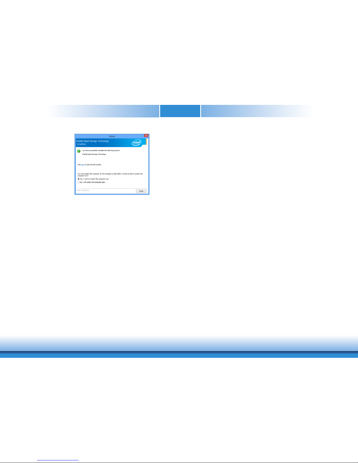
www.d.comChapter 6 RAID
58
Chapter 6
8. Click “Yes, I want to restart
this computer now” to
complete the installation
and then click “Finish”.
Page 59
www.d.comChapter 7 Intel AMT Settings
59
Chapter 7
Chapter 7 - Intel AMT Settings
Overview
Intel Active Management Technology (Intel® AMT) combines hardware and software solution to
provide maximum system defense and protection to networked systems.
The hardware and software information are stored in non-volatile memory. With its built-in
manageability and latest security applications, Intel® AMT provides the following functions.
• Discover
Allows remote access and management of networked systems even while PCs are powered off;
significantly reducing desk-side visits.
• Repair
Remotely repair systems after OS failures. Alerting and event logging help detect problems
quickly to reduce downtime.
• Protect
Intel AMT’s System Defense capability remotely updates all systems with the latest security
software. It protects the network from threats at the source by proactively blocking incoming
threats, reactively containing infected clients before they impact the network, and proactively
alerting when critical software agents are removed.
Enable Intel® AMT in the Insyde BIOS
1. Power-on the system then press <Del> to enter the main menu of the Insyde BIOS.
2. In the Advanced menu, select AMT Configuration.
3. In the Advanced menu, select Enable in the AMT field.
AMT Conguration
ACPI Conguration
CPU Conguration
Video Conguration
Audio Conguration
SATA Conguration
USB Conguration
PCI Express Conguration
ME Conguration
MEBX Conguration
Active Management Technology Supoort
PC Health Status
Main Advanced
F1 Help ↑/↓ Select Item F5/F6 Change Values F9 Setup Defaults
Esc Exit ←/→ Select Item Enter Select SubMenu F10 Save and Exit
InsydeH20 Setup Utility
Security Boot Exit
Rev. 5.0
Active Management Technology Support
Intel AMT Support
Advanced
F1 Help ↑/↓ Select Item F5/F6 Change Values F9 Setup Defaults
Esc Exit ←/→ Select Item Enter Select SubMenu F10 Save and Exit
<Enabled>
Enable/Disable Intel (R)
Active Management Technology BIOS Extension.
Note : iAMT H/W is always enabled. This option
just controls the BIOS
extension execution.
InsydeH20 Setup Utility Rev. 5.0
Page 60
www.d.comChapter 7 Intel AMT Settings
60
Chapter 7
4. In the Save & Exit menu, select Save Changes and Reset then select OK.
Enable Intel® AMT in the Intel® Management
Engine BIOS Extension (MEBX) Screen
1. When the system reboots, you will be prompted for a password. The default password is
“admin”. Enter the default password in the space provided under Intel(R) ME Password
then press Enter.
Exit system setup and save
your changes.
Exit Saving Changes
Load Optimal Defaults
Discard Changes
Main Advanced
F1 Help ↑/↓ Select Item F5/F6 Change Values F9 Setup Defaults
Esc Exit ←/→ Select Item Enter Select SubMenu F10 Save and Exit
InsydeH20 Setup Utility
Security Boot
Rev. 5.0
Exit
Intel(R) Management Engine BIOS Extension v11.0.0.0005/Intel(R) ME v11.0.0.1197
Copyright(C) 2003-15 Intel Corporation. Al l Righ ts Rese rved .
MAIN MENU
MEBx Login
> Intel (R) ME General Settings
> Intel (R) AMT Conguration
MEBx Exit
Intel(R) ME Password
[↑↓] = Move Highlight [Enter] = Select Entry [Esc]= Exit
Page 61
www.d.comChapter 7 Intel AMT Settings
61
Chapter 7
2. Enter a new password in the space provided under Intel(R) ME New Password then press
Enter. The password must include:
• 8-32 characters
• Strong 7-bit ASCII characters excluding : , and ” characters
• At least one digit character (0, 1, ...9)
• At least one 7-bit ASCII non alpha-numeric character, above 0x20, (e.g. !, $, ;)
• Both lower case and upper case characters
Intel(R) Management Engine BIOS Extension v11.0.0.0005/Intel(R) ME v11.0.0.1197
Copyright(C) 2003-15 Intel Corporation. Al l Righ ts Rese rved .
MAIN MENU
MEBx Login
> Intel (R) ME General Settings
> Intel (R) AMT Conguration
MEBx Exit
Intel(R) ME Password
[↑↓] = Move Highlight [Enter] = Select Entry [Esc]= Exit
Intel (R) ME New Password
3. You will be asked to verify the password. Enter the same new password in the space provided under Verify Password then press Enter.
Intel(R) Management Engine BIOS Extension v11.0.0.0005/Intel(R) ME v11.0.0.1197
Copyright(C) 2003-15 Intel Corporation. Al l Righ ts Rese rved .
MAIN MENU
MEBx Login
> Intel (R) ME General Settings
> Intel (R) AMT Conguration
MEBx Exit
Intel(R) ME Password
[↑↓] = Move Highlight [Enter] = Select Entry [Esc]= Exit
Verify Password
4. Select Intel(R) ME General Settings then press Enter.
Intel(R) Management Engine BIOS Extension v11.0.0.0005/Intel(R) ME v11.0.0.1197
Copyright(C) 2003-15 Intel Corporation. Al l Righ ts Rese rved .
MAIN MENU
> Intel (R) ME General Settings
> Intel (R) AMT Conguration
MEBx Exit
[↑↓] = Move Highlight [Enter] = Select Entry [Esc]= Exit
Page 62
www.d.comChapter 7 Intel AMT Settings
62
Chapter 7
5. Select Change Intel(R) ME Password then press Enter.
You will be prompted for a password. The default password is “admin”. Enter the default
password in the space provided under Intel(R) ME New Password then press Enter.
• 8-32 characters
• Strong 7-bit ASCII characters excluding : , and ” characters
• At least one digit character (0, 1, ...9)
• At least one 7-bit ASCII non alpha-numeric character, above 0x20, (e.g. !, $, ;)
• Both lower case and upper case characters
Intel(R) Management Engine BIOS Extension v11.0.0.0005/Intel(R) ME v11.0.0.1197
Copyright(C) 2003-15 Intel Corporation. Al l Righ ts Rese rved .
INTEL (R) ME PLATFORM CONFIGURATION
Change ME Password
Local FW Update <Enabled>
Intel (R) ME New Password
[↑↓] = Move Highlight [Enter] = Select Entry [Esc]= Exit
6. Select Local FW Update then press Enter. Select Enabled then press Enter.
Intel(R) Management Engine BIOS Extension v11.0.0.0005/Intel(R) ME v11.0.0.1197
Copyright(C) 2003-15 Intel Corporation. Al l Righ ts Rese rved .
Change ME Password
Local FW Update <Enabled>
[↑↓] = Move Highlight [Enter] = Complete Entry [Esc]= Discard Changes
Disabled
Enabled
Password Protected
7. Select Previous Menu until you return to the Main Menu. Select Intel(R) AMT Configuration then press Enter.
Intel(R) Management Engine BIOS Extension v11.0.0.0005/Intel(R) ME v11.0.0.1197
Copyright(C) 2003-15 Intel Corporation. Al l Righ ts Rese rved .
INTEL (R) AMT CONFIGURATION
[↑↓] = Move Highlight [Enter] = Select Entry [Esc]= Exit
Manageability Feature Selection < Enabled>
> SOL/Storage Redirection/KVM
> User Consent
Password Policy <Anytime>
> Network Setup
Activate Netwok Access
Uncongure Network Access <Full Unprovision>
> Remote Setup And Conguration
> Power Control
INTEL (R) ME PLATFORM CONFIGURATION
Intel (R) ME New Password
Page 63
www.d.comChapter 7 Intel AMT Settings
63
Chapter 7
8. In the Intel(R) AMT Configuration menu, select Manageability Feature Selection
then press Enter. Select Enabled or Disabled then press Enter.
Intel(R) Management Engine BIOS Extension v11.0.0.0005/Intel(R) ME v11.0.0.1197
Copyright(C) 2003-15 Intel Corporation. Al l Righ ts Rese rved .
Manageability Feature Selection < Enabled>
> SOL/Storage Redirection/KVM
> User Consent
Password Policy <Anytime>
> Network Setup
Activate Netwok Access
Uncongure Network Access <Full Unprovision>
> Remote Setup And Conguration
> Power Control
Disabled
Enabled
9. In the Intel(R) AMT Configuration menu, select SOL/Storage Redirection/KVM
then press Enter.
INTEL (R) AMT CONFIGURATION
10. In the SOL/Storage Redirection/KVM menu, select Username and Password then
press Enter. Select Enabled or Disabled then press Enter.
Intel(R) Management Engine BIOS Extension v11.0.0.0005/Intel(R) ME v11.0.0.1197
Copyright(C) 2003-15 Intel Corporation. Al l Righ ts Rese rved .
SOL/Storage Redirection/KVM
Username and Password <Enabled>
SOL <Enabled>
Storage Redirection <Enabled>
KVM Feature Selection <Enabled>
Disabled
Enabled
11. In the SOL/Storage Redirection/KVM menu, select SOL then press Enter. Select
Enabled or Disabled then press Enter.
[↑↓] = Move Highlight [Enter] = Complete Entry [Esc]= Discard Changes[↑↓] = Move Highlight [Enter] = Complete Entry [Esc]= Discard Changes
Intel(R) Management Engine BIOS Extension v11.0.0.0005/Intel(R) ME v11.0.0.1197
Copyright(C) 2003-15 Intel Corporation. Al l Righ ts Rese rved .
SOL/Storage Redirection/KVM
Username and password <Enabled>
SOL <Enabled>
Storage Redirection <Enabled>
KVM Feature Selection <Enabled>
Disabled
Enabled
[↑↓] = Move Highlight [Enter] = Complete Entry [Esc]= Discard Changes
Intel(R) Management Engine BIOS Extension v11.0.0.0005/Intel(R) ME v11.0.0.1197
Copyright(C) 2003-15 Intel Corporation. Al l Righ ts Rese rved .
Manageability Feature Selection < Enabled>
> SOL/Storage Redirection/KVM
> User Consent
Password Policy <Anytime>
> Network Setup
Activate Netwok Access
Uncongure Network Access <Full Unprovision>
> Remote Setup And Conguration
> Power Control
INTEL (R) AMT CONFIGURATION
[↑↓] = Move Highlight [Enter] = Select Entry [Esc]= Exit
Page 64
www.d.comChapter 7 Intel AMT Settings
64
Chapter 7
12. In the SOL/Storage Redirection/KVM menu, select Storage Redirection then press
Enter. Select Enabled or Disabled then press Enter.
Intel(R) Management Engine BIOS Extension v11.0.0.0005/Intel(R) ME v11.0.0.1197
Copyright(C) 2003-15 Intel Corporation. Al l Righ ts Rese rved .
SOL/Storage Redirection/KVM
Username and password <Enabled>
SOL <Enabled>
Storage Redirection <Enabled>
KVM Feature Selection <Enabled>
Disabled
Enabled
13. In the SOL/Storage Redirection/KVM menu, select KVM Feature Selection then
press Enter. Select Enabled or Disabled then press Enter.
Intel(R) Management Engine BIOS Extension v11.0.0.0005/Intel(R) ME v11.0.0.1197
Copyright(C) 2003-15 Intel Corporation. Al l Righ ts Rese rved .
SOL/Storage Redirection/KVM
Username and password <Enabled>
SOL <Enabled>
Storage Redirection <Enabled>
KVM Feature Selection <Enabled>
Disabled
Enabled
[↑↓] = Move Highlight [Enter] = Complete Entry [Esc]= Discard Changes
[↑↓] = Move Highlight [Enter] = Complete Entry [Esc]= Discard Changes
14. Select Previous Menu until you return to the Intel(R) AMT Configuration menu. Select
User Consent then press Enter.
Intel(R) Management Engine BIOS Extension v11.0.0.0005/Intel(R) ME v11.0.0.1197
Copyright(C) 2003-15 Intel Corporation. Al l Righ ts Rese rved .
[↑↓] = Move Highlight [Enter] = Select Entry [Esc]= Exit
USER CONSENT
User Opt-in < KVM>
Opt-in Congurable from Remote IT < Enabled>
Congure When User Consent Should be Required.
15. In the User Consent menu, select User Opt-in then press Enter. Select None or KVM
or ALL then press Enter.
Intel(R) Management Engine BIOS Extension v11.0.0.0005/Intel(R) ME v11.0.0.1197
Copyright(C) 2003-15 Intel Corporation. Al l Righ ts Rese rved .
USER CONSENT
User Opt-in < KVM>
Opt-in Congurable from Remote IT < Enabled>
NONE
KVM
ALL
[↑↓] = Move Highlight [Enter] = Complete Entry [Esc]= Discard Changes
Page 65
www.d.comChapter 7 Intel AMT Settings
65
Chapter 7
16. In the User Consent menu, select Opt-in Configurable from Remote IT then press
Enter. Select Enabled or Disable Remote Control of KVM Opt-in Policy then press
Enter.
Intel(R) Management Engine BIOS Extension v11.0.0.0005/Intel(R) ME v11.0.0.1197
Copyright(C) 2003-15 Intel Corporation. Al l Righ ts Rese rved .
USER CONSENT
User Opt-in < KVM>
Opt-in Congurable from Remote IT < Enabled>
Enable/Disable Remote Change Capability of User Consent Feature
Disabled
Enabled
17. Select Previous Menu until you return to the Intel(R) AMT Configuration menu. Select
Password Policy then press Enter.
You may choose to use a password only during setup and configuration or to use a pass-
word anytime the system is being accessed.
Intel(R) Management Engine BIOS Extension v11.0.0.0005/Intel(R) ME v11.0.0.1197
Copyright(C) 2003-15 Intel Corporation. Al l Righ ts Rese rved .
Manageability Feature Selection <Enabled>
> SOL/Storage Redirection/KVM
> User Consent
Password Policy <Anytime>
> Network Setup
Activate Netwok Access
Uncongure Network Access <Full Unprovision>
> Remote Setup And Conguration
> Power Control
INTEL (R) AMT CONFIGURATION
Default Password Only
During Step And Conguration
Anytime
[↑↓] = Move Highlight [Enter] = Complete Entry [Esc]= Discard Changes
[↑↓] = Move Highlight [Enter] = Complete Entry [Esc]= Discard Changes
18. In the Intel(R) AMT Configuration menu, select Network Setup then press Enter.
Intel(R) Management Engine BIOS Extension v11.0.0.0005/Intel(R) ME v11.0.0.1197
Copyright(C) 2003-15 Intel Corporation. Al l Righ ts Rese rved .
[↑↓] = Move Highlight [Enter] = Select Entry [Esc]= Exit
Manageability Feature Selection < Enabled>
> SOL/Storage Redirection/KVM
> User Consent
Password Policy <Anytime>
> Network Setup
Activate Network Access
Uncongure Network Access <Full Unprovision>
> Remote Setup And Conguration
> Power Control
INTEL (R) AMT CONFIGURATION
19. In the Intel(R) ME Network Setup menu, select Intel(R) ME Network Name Settings then press Enter.
Intel(R) Management Engine BIOS Extension v11.0.0.0005/Intel(R) ME v11.0.0.1197
Copyright(C) 2003-15 Intel Corporation. Al l Righ ts Rese rved .
[↑↓] = Move Highlight [Enter] = Select Entry [Esc]= Exit
INTEL (R) ME NETWORK SETUP
> Intel (R) ME Network Name Settings
> TCP/ IP Settings
Page 66
www.d.comChapter 7 Intel AMT Settings
66
Chapter 7
20. In the Intel(R) ME Network Name Settings menu, select Host Name then press
Enter. Enter the computer’s host name then press Enter.
Intel(R) Management Engine BIOS Extension v11.0.0.0005/Intel(R) ME v11.0.0.1197
Copyright(C) 2003-15 Intel Corporation. Al l Righ ts Rese rved .
[Enter] = Complete Entry [Esc]= Discard Changes
INTEL (R) ME NETWORK NAME SETTINGS
Host Name _
Domain Name _
Shared/ Dedicated FQDN <Shared>
Dynamic DNS Update <Disabled>
Computer Host Name
21. Select Domain Name then press Enter. Enter the computer’s domain name then press
Enter.
Intel(R) Management Engine BIOS Extension v11.0.0.0005/Intel(R) ME v11.0.0.1197
Copyright(C) 2003-15 Intel Corporation. Al l Righ ts Rese rved .
INTEL (R) ME NETWORK NAME SETTINGS
Host Name _
Domain Name _
Shared/ Dedicated FQDN <Shared>
Dynamic DNS Update <Disabled>
Computer Domain Name
[Enter] = Complete Entry [Esc]= Discard Changes
22. Select Shared/Dedicated FQDN then press Enter. Select Shared or Dedicated then
press Enter.
Intel(R) Management Engine BIOS Extension v11.0.0.0005/Intel(R) ME v11.0.0.1197
Copyright(C) 2003-15 Intel Corporation. Al l Righ ts Rese rved .
INTEL (R) ME NETWORK NAME SETTINGS
Host Name _
Domain Name _
Shared/ Dedicated FQDN <Shared>
Dynamic DNS Update <Disabled>
Dedicated
Shared
23. Select Dynamic DNS Update then press Enter. Select Enabled or Disabled then press
Enter.
Intel(R) Management Engine BIOS Extension v11.0.0.0005/Intel(R) ME v11.0.0.1197
Copyright(C) 2003-15 Intel Corporation. Al l Righ ts Rese rved .
INTEL (R) ME NETWORK NAME SETTINGS
Host Name _
Domain Name _
Shared/ Dedicated FQDN < Shar ed>
Dynamic DNS Update <Disabled>
Disabled
Enabled
[↑↓] = Move Highlight [Enter] = Complete Entry [Esc]= Discard Changes
[↑↓] = Move Highlight [Enter] = Complete Entry [Esc]= Discard Changes
Page 67
www.d.comChapter 7 Intel AMT Settings
67
Chapter 7
24. Select Previous Menu until you return to the Intel(R) ME Network Setup menu. Select
TCP/IP Settings then press Enter.
Intel(R) Management Engine BIOS Extension v11.0.0.0005/Intel(R) ME v11.0.0.1197
Copyright(C) 2003-15 Intel Corporation. Al l Righ ts Rese rved .
[↑↓] = Move Highlight [Enter] = Select Entry [Esc]= Exit
TCP/ IP SETTINGS
> Wired LAN IPV4 Conguration
25. In the TCP/IP Settings menu, select Wired LAN IPV4 Configuration then press
Enter. Select Enabled or Disable IPV4 DHCP Mode then press Enter.
Intel(R) Management Engine BIOS Extension v11.0.0.0005/Intel(R) ME v11.0.0.1197
Copyright(C) 2003-15 Intel Corporation. Al l Righ ts Rese rved .
WIRED LAN IPV4 CONFIGURATION
DHCP Mode <Enabled>
Disabled
Enabled
[↑↓] = Move Highlight [Enter] = Complete Entry [Esc]= Discard Changes
26. In the Intel(R) AMT Configuration menu, select Activate Network Access then
press Enter. Press Y then press Enter.
Intel(R) Management Engine BIOS Extension v11.0.0.0005/Intel(R) ME v11.0.0.1197
Copyright(C) 2003-15 Intel Corporation. Al l Righ ts Rese rved .
INTEL (R) AMT CONFIGURATION
[↑↓] = Move Highlight [Enter] = Select Entry [Esc]= Exit
27. In the Intel(R) AMT Configuration menu, select Unconfigure Network Access then
press Enter.
Intel(R) Management Engine BIOS Extension v11.0.0.0005/Intel(R) ME v11.0.0.1197
Copyright(C) 2003-15 Intel Corporation. Al l Righ ts Rese rved .
INTEL (R) AMT CONFIGURATION
Manageability Feature Selection <Enabled>
> SOL/Storage Redirection/KVM
> User Consent
Password Policy <Anytime>
> Network Setup
Activate Network Access
Uncongure Network Access <Full Unprovision>
> Remote Setup And Conguration
> Power Control
[↑↓] = Move Highlight [Enter] = Complete Entry [Esc]= Discard Changes
Full Unprovision
Manageability Feature Selection < Enabled>
> SOL/Storage Redirection/KVM
> User Consent
Password Policy <Anytime>
> Network Setup
Activate Network Access
Uncongure Network Access <Full Unprovision>
> Remote Setup And Conguration
> Power Control
Activates the current network settings
and opens the ME network interface
Continue: (Y/N)
Page 68
www.d.comChapter 7 Intel AMT Settings
68
Chapter 7
28. In the Intel(R) AMT Configuration menu, select Remote Setup And Configuration
then press Enter.
Intel(R) Management Engine BIOS Extension v11.0.0.0005/Intel(R) ME v11.0.0.1197
Copyright(C) 2003-15 Intel Corporation. Al l Righ ts Rese rved .
[↑↓] = Move Highlight [Enter] = Select Entry [Esc]= Exit
INTEL (R) AMT CONFIGURATION
Manageability Feature Selection < Enabled>
> SOL/Storage Redirection/KVM
> User Consent
Password Policy <Anytime>
> Network Setup
Activate Network Access
Uncongure Network Access <Full Unprovision>
> Remote Setup And Conguration
> Power Control
29. In the Intel(R) Remote Setup And Configuration menu, select Current Provisioing
Mode then press Enter.
Intel(R) Management Engine BIOS Extension v11.0.0.0005/Intel(R) ME v11.0.0.1197
Copyright(C) 2003-15 Intel Corporation. Al l Righ ts Rese rved .
[↑↓] = Move Highlight [Enter] = Select Entry [Esc]= Exit
INTEL (R) REMOTE SETUP AND CONFIGURATION
Current Provisioning Mode
Provisioning Record
Provisioning Server IPV4/IPV6 _
Provisioning Server FQDN _
> RCFG
> TLS PKI
Provisioning Mode: PKI
30. In the Intel(R) Remote Setup And Configuration menu, select Provisioning Record then press Enter.
Intel(R) Management Engine BIOS Extension v11.0.0.0005/Intel(R) ME v11.0.0.1197
Copyright(C) 2003-15 Intel Corporation. Al l Righ ts Rese rved .
INTEL (R) REMOTE SETUP AND CONFIGURATION
Current Provisioning Mode
Provisioning Record
Provisioning Server IPV4/IPV6 _
Provisioning Server FQDN _
> RCFG
> TLS PKI
Provision Record is not present
[↑↓] = Move Highlight [Enter] = Select Entry [Esc]= Exit
31. In the Intel(R) Remote Setup And Configuration menu, select Provisioning server
IPV4/IPV6, enter the Provisioning server address then press Enter.
Intel(R) Management Engine BIOS Extension v11.0.0.0005/Intel(R) ME v11.0.0.1197
Copyright(C) 2003-15 Intel Corporation. Al l Righ ts Rese rved .
INTEL (R) REMOTE SETUP AND CONFIGURATION
Current Provisioning Mode
Provisioning Record
Provisioning Server IPV4/IPV6 _
Provisioning Server FQDN _
> RCFG
> TLS PKI
[Enter] = Complete Entry [Esc]= Discard Changes
Provisioning server address
Page 69
www.d.comChapter 7 Intel AMT Settings
69
Chapter 7
[ESC] = Exit
32. In the Intel(R) Remote Setup And Configuration menu, select Provisioning server
FQDN, enter the FQDN of Provisioning server then press Enter.
Intel(R) Management Engine BIOS Extension v11.0.0.0005/Intel(R) ME v11.0.0.1197
Copyright(C) 2003-15 Intel Corporation. Al l Righ ts Rese rved .
INTEL (R) REMOTE SETUP AND CONFIGURATION
Current Provisioning Mode
Provisioning Record
Provisioning Server IPV4/IPV6 _
Provisioning Server FQDN _
> RCFG
> TLS PKI
Enter FQDN of provisioning server
33. In the Intel(R) Remote Setup And Configuration menu, select RCFG then press
Enter, and select Start Configuration then press enter. Type Y then press enter.
Intel(R) Management Engine BIOS Extension v11.0.0.0005/Intel(R) ME v11.0.0.1197
Copyright(C) 2003-15 Intel Corporation. Al l Righ ts Rese rved .
INTEL (R) REMOTE CONFIGURATION
Start Conguration
[↑↓] = Move Highlight [Enter] = Select Entry [Esc]= Exit
34. In the Intel(R) Remote Setup And Configuration menu, select TLS PKI then press
Enter.
Intel(R) Management Engine BIOS Extension v11.0.0.0005/Intel(R) ME v11.0.0.1197
Copyright(C) 2003-15 Intel Corporation. Al l Righ ts Rese rved .
INTEL (R) REMOTE SETUP AND CONFIGURATION
Current Provisioning Mode
Provisioning Record
Provisioning Server IPV4/IPV6 _
Provisioning Server FQDN _
> RCFG
> TLS PKI
[↑↓] = Move Highlight [Enter] = Select Entry [Esc]= Exit
35. In the Intel(R) Remote Configuration menu, select Remote Configuration** then
press Enter, select Enabled or Disabled then press Enter.
Intel(R) Management Engine BIOS Extension v11.0.0.0005/Intel(R) ME v11.0.0.1197
Copyright(C) 2003-15 Intel Corporation. Al l Righ ts Rese rved .
INTEL (R) REMOTE CONFIGURATION
Remote Conguration** < Enabled>
PKI DNS Sufx _
> Manage Hashes
Disabled
Enabled
This will activate Remote Condiguration.
Continue: (Y/N)
[Enter] = Complete Entry [Esc]= Discard Changes
[↑↓] = Move Highlight [Enter] = Complete Entry [Esc]= Discard Changes
Page 70
www.d.comChapter 7 Intel AMT Settings
70
Chapter 7
36. In the Intel(R) Remote Configuration menu, select PKI DNS Suffix then press
Enter. Type PKI DNS Suffix then press Enter.
Intel(R) Management Engine BIOS Extension v11.0.0.0005/Intel(R) ME v11.0.0.1197
Copyright(C) 2003-15 Intel Corporation. Al l Righ ts Rese rved .
INTEL (R) REMOTE CONFIGURATION
Remote Conguration** < Enabled>
PKI DNS Sufx _
> Manage Hashes
Enter PKI DNS Sufx
37. Select Manage Hashes then press Enter, and select one of hash name.
Intel(R) Management Engine BIOS Extension v11.0.0.0005/Intel(R) ME v11.0.0.1197
Copyright(C) 2003-15 Intel Corporation. Al l Righ ts Rese rved .
INTEL (R) REMOTE CONFIGURATION
Remote Conguration** < Enabled>
PKI DNS Sufx _
> Manage Hashes
[↑↓] = Move Highlight [Enter] = Select Entry [Esc]= Exit
38. In the Intel(R) Remote Configuration menu, select Manage Hashes then press
Enter.
Intel(R) Management Engine BIOS Extension v11.0.0.0005/Intel(R) ME v11.0.0.1197
Copyright(C) 2003-15 Intel Corporation. Al l Righ ts Rese rved .
INTEL (R) REMOTE CONFIGURATION
[Ins]= Add New Hash [Delete] = Delete Hash [+] = Activate Hash
[↑↓] =Move Highlight [Enter] = View Hash [Esc]= Exit
Active: [*]
Active: [*]
Active: [*]
Active: [*]
Active: [*]
Active: [*]
Active: [*]
Active: [*]
Active: [*]
Active: [*]
Active: [*]
Active: [*]
Active: [*]
Active: [*]
Active: [*]
Active: [*]
Active: [*]
Active: [*]
Default: [*]
Default: [*]
Default: [*]
Default: [*]
Default: [*]
Default: [*]
Default: [*]
Default: [*]
Default: [*]
Default: [*]
Default: [*]
Default: [*]
Default: [*]
Default: [*]
Default: [*]
Default: [*]
Default: [*]
Default: [*]
SHA256
SHA256
SHA256
SHA256
SHA256
SHA256
SHA256
SHA256
SHA256
SHA256
SHA256
SHA256
SHA256
SHA256
SHA256
SHA256
SHA256
SHA256
Hash Name Active Default Algorithm
VeriSign Class 3
VeriSign Class 3
Go Daddy Class 2
Comodo AAA CA
Stareld Class 2
VeriSign Class 3
VeriSign Class 3
VeriSign Class 3
GTE CyberTrust G1
Baltimore Cyber Tr
Cyber Trust Global
Verizon Global Ro
Entrust. net CA (2
Entrust Root CA
VeriSign Universa
Go Daddy Root CA
Entrust Root CA -
Starteld Root CA
39. In the Intel(R) AMT Configuration menu, select Power Control then press Enter.
Intel(R) Management Engine BIOS Extension v11.0.0.0005/Intel(R) ME v11.0.0.1197
Copyright(C) 2003-15 Intel Corporation. Al l Righ ts Rese rved .
[↑↓] = Move Highlight [Enter] = Select Entry [Esc]= Exit
Manageability Feature Selection <Enabled>
> SOL/ Storage Redirection/KVM
> User Consent
Password Policy <Anytime>
> Network Setup
Activate Netwok Access
Uncongure Network Access <Full Unprovision>
> Remote Setup And Conguration
> Power Control
INTEL (R) AMT CONFIGURATION
[Enter] = Complete Entry [Esc]= Discard Changes
Page 71
www.d.comChapter 7 Intel AMT Settings
71
Chapter 7
42. Select Previous Menu until you return to the Main Menu. Select Exit then press Enter.
Type Y then press Enter.
Intel(R) Management Engine BIOS Extension v11.0.0.0005/Intel(R) ME v11.0.0.1197
Copyright(C) 2003-15 Intel Corporation. Al l Righ ts Rese rved .
MAIN MENU
> Intel (R) ME General Settings
> Intel (R) AMT Conguration
MEBx Exit
Exit
[↑↓] = Move Highlight [Enter] = Select Entry [Esc]= Exit
40. In the Intel(R) AMT Power Control menu, select Intel(R) AMT ON in Host Sleep
States then press Enter. Select an option then press Enter.
Intel(R) Management Engine BIOS Extension v11.0.0.0005/Intel(R) ME v11.0.0.1197
Copyright(C) 2003-15 Intel Corporation. Al l Righ ts Rese rved .
INTEL (R) AMT POWER CONTROL
Mobile: ON in S0
Mobile: ON in S0, ME Wake in S3, S4-5 (AC only)
Intel (R) AMT ON in Host Sleep States <Mobile: ON in S0,
ME Wake in S3, S4-5
(AC only)>
Idle Timeout 65535
[↑↓] = Move Highlight [Enter] = Complete Entry [Esc]= Discard Changes
These congurations are effective only after AMT provisioning has started
MAIN MENU
41. In the Intel(R) AMT Power Control menu, select Idle Timeout then press Enter.
Enter the timeout value (1-65535).
Intel(R) Management Engine BIOS Extension v11.0.0.0005/Intel(R) ME v11.0.0.1197
Copyright(C) 2003-15 Intel Corporation. Al l Righ ts Rese rved .
INTEL (R) AMT POWER CONTROL
This congurations are effective only after AMT provisioning has started
Intel (R) ME ON in Host Sleep States <Mobile: ON in S0,
ME Wake in S3, S4-5
(AC only)>
Idle Timeout 65535
<ENTER> = Complete Entry [ESC]= Discard Changes
Timeout Value (1-65535)
65535
Page 72

www.d.comAppendix A Troubleshooting
72
Appendix A
Appendix A - Troubleshooting
Troubleshooting Checklist
This chapter of the manual is designed to help you with problems that you may encounter
with your personal computer. To efficiently troubleshoot your system, treat each problem individually. This is to ensure an accurate diagnosis of the problem in case a problem has multiple
causes.
Some of the most common things to check when you encounter problems while using your
system are listed below.
1. The power switch of each peripheral device is turned on.
2. All cables and power cords are tightly connected.
3. The electrical outlet to which your peripheral devices are connected is working. Test the
outlet by plugging in a lamp or other electrical device.
4. The monitor is turned on.
5. The display’s brightness and contrast controls are adjusted properly.
6. All add-in boards in the expansion slots are seated securely.
7. Any add-in board you have installed is designed for your system and is set up correctly.
Monitor/Display
If the display screen remains dark after the system is turned on:
1. Make sure that the monitor’s power switch is on.
2. Check that one end of the monitor’s power cord is properly attached to the monitor and the
other end is plugged into a working AC outlet. If necessary, try another outlet.
3. Check that the video input cable is properly attached to the monitor and the system’s
display adapter.
4. Adjust the brightness of the display by turning the monitor’s brightness control knob.
The picture seems to be constantly moving.
1. The monitor has lost its vertical sync. Adjust the monitor’s vertical sync.
2. Move away any objects, such as another monitor or fan, that may be creating a magnetic
field around the display.
3. Make sure your video card’s output frequencies are supported by this monitor.
The screen seems to be constantly wavering.
1. If the monitor is close to another monitor, the adjacent monitor may need to be turned off.
Fluorescent lights adjacent to the monitor may also cause screen wavering.
Power Supply
When the computer is turned on, nothing happens.
1. Check that one end of the AC power cord is plugged into a live outlet and the other end
properly plugged into the back of the system.
2. Make sure that the voltage selection switch on the back panel is set for the correct type of
voltage you are using.
3. The power cord may have a “short” or “open”. Inspect the cord and install a new one if
necessary.
Page 73

www.d.comAppendix A Troubleshooting
73
Appendix A
Hard Drive
Hard disk failure.
1. Make sure the correct drive type for the hard disk drive has been entered in the BIOS.
2. If the system is configured with two hard drives, make sure the bootable (first) hard drive
is configured as Master and the second hard drive is configured as Slave. The master hard
drive must have an active/bootable partition.
Excessively long formatting period.
If your hard drive takes an excessively long period of time to format, it is likely a cable connection problem. However, if your hard drive has a large capacity, it will take a longer time to
format.
Serial Port
The serial device (modem, printer) doesn’t output anything or is outputting garbled
characters.
1. Make sure that the serial device’s power is turned on and that the device is on-line.
2. Verify that the device is plugged into the correct serial port on the rear of the computer.
3. Verify that the attached serial device works by attaching it to a serial port that is work-
ing and configured correctly. If the serial device does not work, either the cable or the serial
device has a problem. If the serial device works, the problem may be due to the onboard I/O
or the address setting.
4. Make sure the COM settings and I/O address are configured correctly.
Keyboard
Nothing happens when a key on the keyboard was pressed.
1. Make sure the keyboard is properly connected.
2. Make sure there are no objects resting on the keyboard and that no keys are pressed dur-
ing the booting process.
System Board
1. Make sure the add-in card is seated securely in the expansion slot. If the add-in card is
loose, power off the system, re-install the card and power up the system.
2. Check the jumper settings to ensure that the jumpers are properly set.
3. Verify that all memory modules are seated securely into the memory sockets.
4. Make sure the memory modules are in the correct locations.
5. If the board fails to function, place the board on a flat surface and seat all socketed components. Gently press each component into the socket.
6. If you made changes to the BIOS settings, re-enter setup and load the BIOS defaults.
Page 74
www.d.comAppendix B Insyde BIOS Standard Status POST Code
74
Appendix B
Appendix B - Insyde BIOS Standard Status POST Code
SEC Phase 8-Bit POST Code Values
Functionality Name POST Code Value Description
SEC_SYSTEM_POWER_ON 01 CPU power on and switch to Protected mode
SEC_AFTER_MICROCODE_PATCH 03 Setup Cache as RAM
SEC_ACCESS_CSR 04 PCIE MMIO Base Address initial
SEC_GENERIC_MSRINIT 05 CPU Generic MSR initialization
SEC_CPU_SPEEDCFG 06 Setup CPU speed
SEC_SETUP_CAR_OK 07 Cache as RAM test
SEC_FORCE_MAX_RATIO 08 Tune CPU frequency ratio to maximum level
SEC_GO_TO_SECSTARTUP 09 Setup BIOS ROM cache
SEC_GO_TO_PEICORE 0A Enter Boot Firmware Volume
P
EI Phase 8-Bit POST Code Values
Functionality Name POST Code Value Description
PEI_SIO_INIT 70 Super I/O initialization
PEI_CPU_REG_INIT 71 CPU Early Initialization
PEI_CPU_AP_INIT 72 Multi-processor Early initialization
PEI_CPU_HT_RESET 73 HyperTransport initialization
PEI_PCIE_MMIO_INIT 74 PCIE MMIO BAR Initialization
PEI_NB_REG_INIT 75 North Bridge Early Initialization
PEI_SB_REG_INIT 76 South Bridge Early Initialization
PEI_PCIE_TRAINING 77 PCIE Training
PEI_TPM_INIT 78 TPM Initialization
PEI_MEMORY_INSTALL 80 Simple Memory test
PEI_TXTPEI 81 TXT function early initialization
PEI_MEMORY_CALLBACK 83 Set cache for physical memory
D
XE Phase 8-Bit POST Code Values
Functionality Name Post Code Values Description
DXE_SB_SPI_INIT 41 South bridge SPI initialization
DXE_VARIABLE_RECLAIM 61 Variable store garbage collection and reclaim operation
DXE_FLASH_PART_NONSUPPORT 62 Flash part not supported.
B
DS Phase 8-Bit POST Code Values
Functionality Name
POST Code Value
Description
BDS_ENTER_BDS 10 Enter BDS entry
BDS_INSTALL_HOTKEY 11 Install Hotkey service
BDS_ASF_INIT 12 ASF Initialization
BDS_PCI_ENUMERATION_START 13 PCI enumeration
BDS_BEFORE_PCIIO_INSTALL 14 PCI resource assign complete
BDS_PCI_ENUMERATION_END 15 PCI enumeration complete
BDS_CONNECT_CONSOLE_IN 16 Keyboard Controller, Keyboard and Mouse initializatio
BDS_CONNECT_CONSOLE_OUT 17 Video device initialization
BDS_CONNECT_STD_ERR 18 Error report device initialization
BDS_CONNECT_USB_HC 19 USB host controller initialization
BDS_CONNECT_USB_BUS 1A USB BUS driver initialization
BDS_CONNECT_USB_DEVICE 1B USB device driver initialization
BDS_NO_CONSOLE_ACTION 1C Console device initialization fail
BDS_ENUMERATE_ALL_BOOT_OPTIO
N
27 Get boot device information
BDS_ENTER_SETUP 29 Enter Setup Menu
BDS_ENTER_BOOT_MANAGER 2A Enter Boot manager
BDS_READY_TO_BOOT_EVENT 2E Last Chipset initialization before boot to OS
BDS_GO_LEGACY_BOOT 2F Start to boot Legacy OS
BDS_GO_UEFI_BOOT 30 Start to boot UEFI OS
BDS_LEGACY16_PREPARE_TO_BOOT 31 Prepare to Boot to Legacy OS
BDS_EXIT_BOOT_SERVICES 32 Send END of POST Message to ME via HECI
SEC Phase 8-Bit POST Code Values
Functionality Name POST Code Value Description
SEC_SYSTEM_POWER_ON 01 CPU power on and switch to Protected mode
SEC_AFTER_MICROCODE_PATCH 03 Setup Cache as RAM
SEC_ACCESS_CSR 04 PCIE MMIO Base Address initial
SEC_GENERIC_MSRINIT 05 CPU Generic MSR initialization
SEC_CPU_SPEEDCFG 06 Setup CPU speed
SEC_SETUP_CAR_OK 07 Cache as RAM test
SEC_FORCE_MAX_RATIO 08 Tune CPU frequency ratio to maximum level
SEC_GO_TO_SECSTARTUP 09 Setup BIOS ROM cache
SEC_GO_TO_PEICORE 0A Enter Boot Firmware Volume
P
EI Phase 8-Bit POST Code Values
Functionality Name POST Code Value Description
PEI_SIO_INIT 70 Super I/O initialization
PEI_CPU_REG_INIT 71 CPU Early Initialization
PEI_CPU_AP_INIT 72 Multi-processor Early initialization
PEI_CPU_HT_RESET 73 HyperTransport initialization
PEI_PCIE_MMIO_INIT 74 PCIE MMIO BAR Initialization
PEI_NB_REG_INIT 75 North Bridge Early Initialization
PEI_SB_REG_INIT 76 South Bridge Early Initialization
PEI_PCIE_TRAINING 77 PCIE Training
PEI_TPM_INIT 78 TPM Initialization
PEI_MEMORY_INSTALL 80 Simple Memory test
PEI_TXTPEI 81 TXT function early initialization
PEI_MEMORY_CALLBACK 83 Set cache for physical memory
D
XE Phase 8-Bit POST Code Values
Functionality Name Post Code Values Description
DXE_SB_SPI_INIT 41 South bridge SPI initialization
DXE_VARIABLE_RECLAIM 61 Variable store garbage collection and reclaim operation
DXE_FLASH_PART_NONSUPPORT 62 Flash part not supported.
B
DS Phase 8-Bit POST Code Values
Functionality Name
POST Code Value
Description
BDS_ENTER_BDS 10 Enter BDS entry
BDS_INSTALL_HOTKEY 11 Install Hotkey service
BDS_ASF_INIT 12 ASF Initialization
BDS_PCI_ENUMERATION_START 13 PCI enumeration
BDS_BEFORE_PCIIO_INSTALL 14 PCI resource assign complete
BDS_PCI_ENUMERATION_END 15 PCI enumeration complete
BDS_CONNECT_CONSOLE_IN 16 Keyboard Controller, Keyboard and Mouse initializatio
BDS_CONNECT_CONSOLE_OUT 17 Video device initialization
BDS_CONNECT_STD_ERR 18 Error report device initialization
BDS_CONNECT_USB_HC 19 USB host controller initialization
BDS_CONNECT_USB_BUS 1A USB BUS driver initialization
BDS_CONNECT_USB_DEVICE 1B USB device driver initialization
BDS_NO_CONSOLE_ACTION 1C Console device initialization fail
BDS_ENUMERATE_ALL_BOOT_OPTIO
N
27 Get boot device information
BDS_ENTER_SETUP 29 Enter Setup Menu
BDS_ENTER_BOOT_MANAGER 2A Enter Boot manager
BDS_READY_TO_BOOT_EVENT 2E Last Chipset initialization before boot to OS
BDS_GO_LEGACY_BOOT 2F Start to boot Legacy OS
BDS_GO_UEFI_BOOT 30 Start to boot UEFI OS
BDS_LEGACY16_PREPARE_TO_BOOT 31 Prepare to Boot to Legacy OS
BDS_EXIT_BOOT_SERVICES 32 Send END of POST Message to ME via HECI
P
ostBDS Phase 8-Bit POST Code Values
Functionality Name POST Code Value Description
POST_BDS_NO_BOOT_DEVICE F9 No Boot Device
POST_BDS_JUMP_BOOT_SECTOR FE Try to Boot with INT 19
A
CPI 8-Bit POST Code Values
Functionality Name POST Code Value Description
ASL_ENTER_S1 51 Prepare to enter S1
ASL_ENTER_S3 53 Prepare to enter S3
ASL_ENTER_S4 54 Prepare to enter S4
ASL_ENTER_S5 55 Prepare to enter S5
ASL_WAKEUP_S1 E1 System wakeup from S1
ASL_WAKEUP_S3 E3 System wakeup from S3
ASL_WAKEUP_S4 E4 System wakeup from S4
ASL_WAKEUP_S5 E5 System wakeup from S5
S
MM 8-Bit POST Code Values
Functionality Name POST Code Value Description
SMM_ACPI_ENABLE_END A7 ACPI enable function complete
SMM_S1_SLEEP_CALLBACK A1 Enter S1
SMM_S3_SLEEP_CALLBACK A3 Enter S3
SMM_S4_SLEEP_CALLBACK A4 Enter S4
SMM_S5_SLEEP_CALLBACK A5 Enter S5
 Loading...