

Page 1
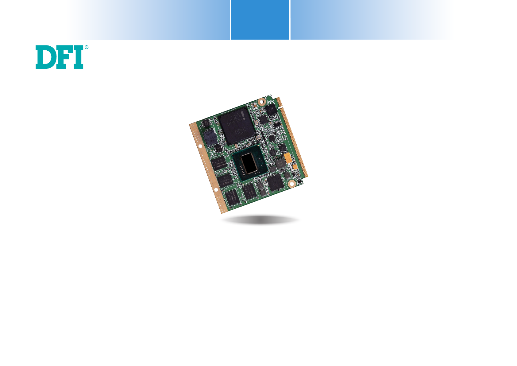
QB702-B
Qseven Board
User’s Manual
A24720340
1
www.d.comChapter 1 Introduction
Page 2

Copyright
FCC and DOC Statement on Class B
This publication contains information that is protected by copyright. No part of it may be reproduced in any form or by any means or used to make any transformation/adaptation without
the prior written permission from the copyright holders.
This publication is provided for informational purposes only. The manufacturer makes no
representations or warranties with respect to the contents or use of this manual and specifically disclaims any express or implied warranties of merchantability or fitness for any particular
purpose. The user will assume the entire risk of the use or the results of the use of this document. Further, the manufacturer reserves the right to revise this publication and make changes
to its contents at any time, without obligation to notify any person or entity of such revisions
or changes.
Changes after the publication’s first release will be based on the product’s revision. The website
will always provide the most updated information.
© 2013. All Rights Reserved.
Trademarks
Product names or trademarks appearing in this manual are for identification purpose only and
are the properties of the respective owners.
Qseven Specification Reference
http://www.qseven-standard.org/
This equipment has been tested and found to comply with the limits for a Class B digital
device, pursuant to Part 15 of the FCC rules. These limits are designed to provide reasonable protection against harmful interference when the equipment is operated in a residential
installation. This equipment generates, uses and can radiate radio frequency energy and, if not
installed and used in accordance with the instruction manual, may cause harmful interference
to radio communications. However, there is no guarantee that interference will not occur in a
particular installation. If this equipment does cause harmful interference to radio or television
reception, which can be determined by turning the equipment off and on, the user is encouraged to try to correct the interference by one or more of the following measures:
• Reorient or relocate the receiving antenna.
• Increase the separation between the equipment and the receiver.
• Connect the equipment into an outlet on a circuit different from that to which the receiver
is connected.
• Consult the dealer or an experienced radio TV technician for help.
Notice:
1. The changes or modifications not expressly approved by the party responsible for compliance could void the user’s authority to operate the equipment.
2. Shielded interface cables must be used in order to comply with the emission limits.
2
www.dfi .comChapter 1 Introduction
Page 3

Table of Contents
Save & Exit ................................................................................................ 28
Updating the BIOS .......................................................................................29
Copyright .............................................................................................................2
Trademarks ........................................................................................................2
FCC and DOC Statement on Class B .....................................................2
About this Manual ..........................................................................................4
Warranty ............................................................................................................4
Static Electricity Precautions ......................................................................4
Safety Measures ..............................................................................................4
About the Package .........................................................................................5
Chapter 1 - Introduction .............................................................................6
Specifications ................................................................................................6
Features ..........................................................................................................7
Chapter 2 - Hardware Installation ................................................ 8
Board Layout .................................................................................................8
Block Diagram ...............................................................................................8
Mechanical Diagram ....................................................................................9
System Memory ..........................................................................................10
Cooling Option ............................................................................................10
MXM Connector ..........................................................................................11
MXM Connector Signal Description .......................................................13
Installing QB702-B Series onto a Carrier Board ...............................19
Chapter 4 - Supported Software .......................................................... 30
Appendix A - nLite and AHCI Installation Guide ...........................39
nLite ...............................................................................................................39
AHCI ..............................................................................................................43
Appendix B - System Error Message ...................................................45
Appendix C - Troubleshooting ................................................................46
Chapter 3 - BIOS Setup ............................................................... 20
Overview ..................................................................................................... 20
AMI BIOS Setup Utility .............................................................................21
Main ..........................................................................................................21
Advanced ...................................................................................................21
Chipset ......................................................................................................24
Boot...........................................................................................................27
Security ...................................................................................................... 28
3
www.dfi .comChapter 1 Introduction
Page 4
About this Manual
Static Electricity Precautions
An electronic file of this manual is included in the CD. To view the user’s manual in the CD,
insert the CD into a CD-ROM drive. The autorun screen (Main Board Utility CD) will appear.
Click “User’s Manual” on the main menu.
Warranty
1. Warranty does not cover damages or failures that arised from misuse of the product,
inability to use the product, unauthorized replacement or alteration of components and
product specifications.
2. The warranty is void if the product has been subjected to physical abuse, improper installation, modification, accidents or unauthorized repair of the product.
3. Unless otherwise instructed in this user’s manual, the user may not, under any circumstances, attempt to perform service, adjustments or repairs on the product, whether in or
out of warranty. It must be returned to the purchase point, factory or authorized service
agency for all such work.
4. We will not be liable for any indirect, special, incidental or consequencial damages to the
product that has been modified or altered.
It is quite easy to inadvertently damage your PC, system board, components or devices even
before installing them in your system unit. Static electrical discharge can damage computer
components without causing any signs of physical damage. You must take extra care in handling them to ensure against electrostatic build-up.
1. To prevent electrostatic build-up, leave the system board in its anti-static bag until you are
ready to install it.
2. Wear an antistatic wrist strap.
3. Do all preparation work on a static-free surface.
4. Hold the device only by its edges. Be careful not to touch any of the components, contacts
or connections.
5. Avoid touching the pins or contacts on all modules and connectors. Hold modules or connectors by their ends.
Important:
Electrostatic discharge (ESD) can damage your processor, disk drive and other components. Perform the upgrade instruction procedures described at an ESD workstation only. If such a station is not available, you can provide some ESD protection by
wearing an antistatic wrist strap and attaching it to a metal part of the system chassis. If a wrist strap is unavailable, establish and maintain contact with the system
chassis throughout any procedures requiring ESD protection.
Safety Measures
To avoid damage to the system:
• Use the correct AC input voltage range.
To reduce the risk of electric shock:
• Unplug the power cord before removing the system chassis cover for installation or servicing. After installation or servicing, cover the system chassis before plugging the power
cord.
4
www.dfi .comChapter 1 Introduction
Page 5

About the Package
The package contains the following items. If any of these items are missing or damaged,
please contact your dealer or sales representative for assistance.
• One QB702-B board
• One DVD
• One QR (Quick Reference)
Optional Items
• Q7-100 carrier board kit
• Two standoff bolts
• Two sets of nut and bolt
• One bracket
• Heat spreader with heat sink
• Heat spreader
The board and accessories in the package may not come similar to the information listed
above. This may differ in accordance with the sales region or models in which it was sold. For
more information about the standard package in your region, please contact your dealer or
sales representative.
5
www.dfi .comChapter 1 Introduction
Page 6
Chapter 1 - Introduction
Specifications
Processor
Chipset
System Memory
Graphics
Audio
LAN
Serial ATA
SDIO/MMC
Interface
Trusted
Platform
Module-TPM
(optional)
SSD
(optional)
• QB702-B620T102
®
- Intel
• QB702-B640T102
- Intel
• QB702-B660T102
- Intel
• QB702-B680T102
- Intel
• Intel® EG20T PCH
• 1GB DDR2 onboard
• Supports memory down (single 32-bit channel)
• Intel® GMA 600
• Supports up to 400MHz graphics frequency
• Ultra low power integrated 3D graphics
• High defi nition hardware video decoder and encoder engine
• Supports LVDS and SDVO interfaces
- LVDS: Supports pixel clock depths of 18/24-bit, single channel, max. pixel
- SDVO: Up to 160MHz pixel clock, equates to 1280x1024 @ 85Hz
• Supports High Defi nition Audio interface
• Integrated Intel® PCH GbE MAC
• One Micrel KSZ9021RNI Ethernet PHY
• Supports 10Mbps, 100Mbps and 1Gbps data transmission
• IEEE 802.3 (10/100Mbps) and IEEE 802.3ab (1Gbps) compliant
• Supports 2 SATA interfaces
- One port shared with SSD
• SATA speed up to 3Gb/s (SATA 2.0)
• Supports 1 SDIO/MMC
• Supports SDA Standard Ver 1.0, SD memory card specifi cation Ver 2.0,
SDIO card specifi cation Ver 1.0, MMC System specifi cation Ver 4.1
• Conforms to Secure Digital Host Controller (SDHC) speed class 6
• Provides a Trusted PC for secure transactions
• Provides software license protection, enforcement and password protection
• 2GB/4GB/8GB/16GB/32GB
AtomTM E620T (512KB L2 cache, 600 MHz, 3.3W)
®
AtomTM E640T (512KB L2 cache, 1.0 GHz, 3.6W)
®
AtomTM E660T (512KB L2 cache, 1.3 GHz, 3.6W)
®
AtomTM E680T (512KB L2 cache, 1.6 GHz, 4.5W)
clock of 80MHz, equates to 1280x768 @ 60Hz
Chapter 1
Expansion
Interfaces
Energy Effi cient
Design
BIOS
Watchdog
Timer
Power
Power
Consumption
OS Support
Temperature
Humidity
PCB
• Supports 8 USB 2.0 interfaces:
- 7 Host and 1 Host/Client (selectable)
• Supports 1 LPC interface
• Supports 1 SMBus interface
• Supports 1 I
• Supports 3 PCIe x1 interfaces
• Supports CAN-bus (Controller-Area Network) interface
• Supports ExpressCard (PCIe signal only)
• Supports 1 serial interface (TX/RX)
• Supports 8-bit DIO interface
• Supports ACPI 2.0/1.0 specifi cation
• Enhanced Intel
• AMI BIOS
- 16Mbit SPI Flash BIOS (UEFI BIOS)
• Software programmable from 1 to 255 seconds
• Input: VCC_RTC, 5V standby, 5V
• Supports ATX/AT mode
• 7.6 W with E680 at 1.6GHz and 1GB DDR2 onboard
• Windows XP Professional x86 & SP3 (32-bit)
• Operating: -40oC to 85oC
• Storage: -40
• 10% to 90%
• Dimensions
- Qseven form factor
- 70mm (2.76") x 70mm (2.76")
• Compliance
- Qseven specifi cation revision 1.2
2
C interface
®
SpeedStep Technology
o
C to 85oC
6
www.dfi .comChapter 1 Introduction
Page 7
Chapter 1
A
g
p
)
p
g
play
,
A
/Gig
t
p
t
y
g
r
p
)
y
Features
• DDR2
DDR2 is a higher performance DDR technology whose data transfer rate delivers bandwidth
of 4.3 GB per second and beyond. That is twice the speed of the conventional DDR without
increasing its power consumption. DDR2 SDRAM modules work at 1.8V supply compared to
2.6V memory voltage for DDR modules. DDR2 also incorporates new innovations such as the
On-Die Termination (ODT) as well as larger 4-bit pre-fetch against DDR which fetches 2 bits
per clock cycle.
• Graphics
The integrated Intel® HD graphics engine delivers an excellent blend of graphics performance
and features to meet business needs. It provides excellent video and 3D graphics with outstanding graphics responsiveness. These enhancements deliver the performance and compatibility needed for today’s and tomorrow’s business applications. Supports LVDS and SDVO
display outputs.
• Serial ATA
Serial ATA is a storage interface that is compliant with SATA 2.0a specification. With speed of
up to 3Gb/s (SATA 2.0), it improves hard drive performance faster than the standard parallel
ATA whose data transfer rate is 100MB/s. The bandwidth of the SATA 3.0 will be limited by
carrier board design.
• Gigabit LAN
The Micrel KSZ9021RNI Ethernet Phy controller supports up to 1Gbps data transmission.
Specification Comparison Table
The table below shows the Qseven standard specifications and the corresponding
specifications supported on the QB702-B module.
System I/O Interface
PCI Ex
ress Lanes 0 1 (x1 link
Serial ATA channels 0 0 2 2
orts 3 4 8 8
USB 2.0
LVDS channels 0 0 Dual Channel 24bits Sin
Port, TMDS
Dis
High Definition
udio/AC'97
Ethernet 10/100
abi
Mbit
ressCard support0022
Ex
Low Pin Count bus 0 0 1 1
Secure Digital I/O 8-bi
for SD/MMC cards
stem Management 0 1 1 1
S
2
C Bus
I
SPI Bus 0 0 1 1
CAN Bus 0 0 1 1
Trigge
Watchdo
Power Button 1 1 1 1
Power Good 1 1 1 1
Reset Button 1 1 1 1
LID Button 0 0 1 1
Button 0 0 1 1
Slee
Suspend To RAM (S3
mode
Wake 0 0 1 1
low alarm 0 0 1 1
Batter
Thermal control 0 0 1 1
FAN control 0 0 1 1
RM/RISC Based
Minimum Confi
0011
0011
0 0 1 (Gigabit Ethernet) 1
0011
1111
1111
0011
uration
X86 Based Minimum
Configuration
Maximum
Configuration
43
DFI QB702
Configuration
le Channel 24bits
• Watchdog Timer
The Watchdog Timer function allows your application to regularly “clear” the system at the set
time interval. If the system hangs or fails to function, it will reset at the set time interval so
that your system will continue to operate.
7
www.dfi .comChapter 1 Introduction
Page 8
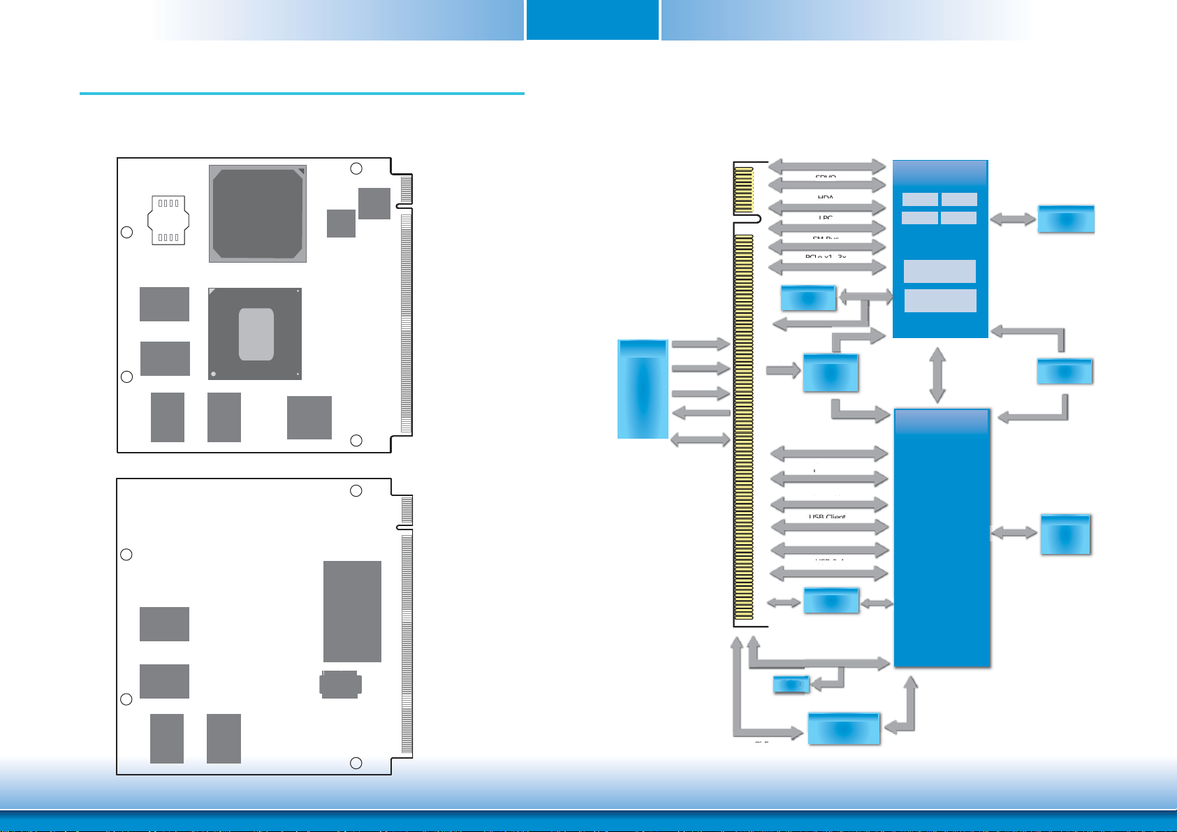
Chapter 2 - Hardware Installation
5
SDVO
HDA
LPC
PCIe x1 3x
SM Bus
LVDS
USB 04
USB Client
SDIO/MMC
CAN Bus
I
C Bus
SSD
SPI
Board Layout
SPI Flash
BIOS
DDR2
DDR2
DDR2
Intel
EG20T
Intel Atom E6xxT
DDR2
PMIC
USB
HUB
GLAN
PHY
Top View
Chapter 2
Block Diagram
AMXM Golden Finger
Micro
controller-
PIC16F690
WDTO
LVDS_DIMMING
CB_PWRBTN
WDI
2
I
C_DAT/CLO
SPI Flash
16Mbit
+5V
LVDS
SDVO
HDA
LPC
SM Bus
PCIe x1 3x
PMIC
DC/DC
LDO
SDIO/MMC
2
C Bus
I
CAN Bus
SPI
Processor
CORE
CORE
CORE
CORE
Atom E6xx Series
Graphics
CORE
Memory
Controller
PCIe x1
DDR2
1Gbit x8
CLK Gen
8x
DDR2
DDR2
DDR2
DDR2
SSD
TPM
Bottom View
USB Client
Serial RX/TX
USB 0-4
EG20T
SPI
EEPROM
USB Hub
USB 5-7
SATA 2x
SSD
GbE
8
KSZ9021RNI
USB 5
Port 1 (optional)
PHY
GMII
www.dfi .comChapter 2 Hardware Installation
Page 9
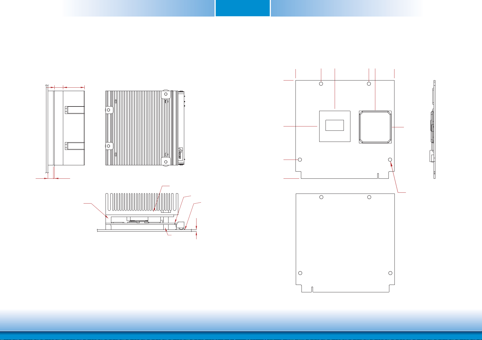
Mechanical Diagram
Chapter 2
QB702-B Module with thermal solution
0.00
8.00 20.20
0
1.20
Heatspreader
Heatsink
Module PCB
Carrier PCB
0.00
32.86
56.50
70.00
QB702-B Module
27.74
18.00
52.00
56.48
70.00
Top View
33.33
Ø2.50 (*4pcs)
1.60
Standoff
Side View of the Module with thermal solution and Carrier Board
Bottom View
9
www.dfi .comChapter 2 Hardware Installation
Page 10
Chapter 2
Important:
Electrostatic discharge (ESD) can damage your processor, disk drive and other components. Perform the upgrade instruction procedures described at an ESD workstation only. If such a station is not available, you can provide some ESD protection by
wearing an antistatic wrist strap and attaching it to a metal part of the system chassis. If a wrist strap is unavailable, establish and maintain contact with the system
chassis throughout any procedures requiring ESD protection.
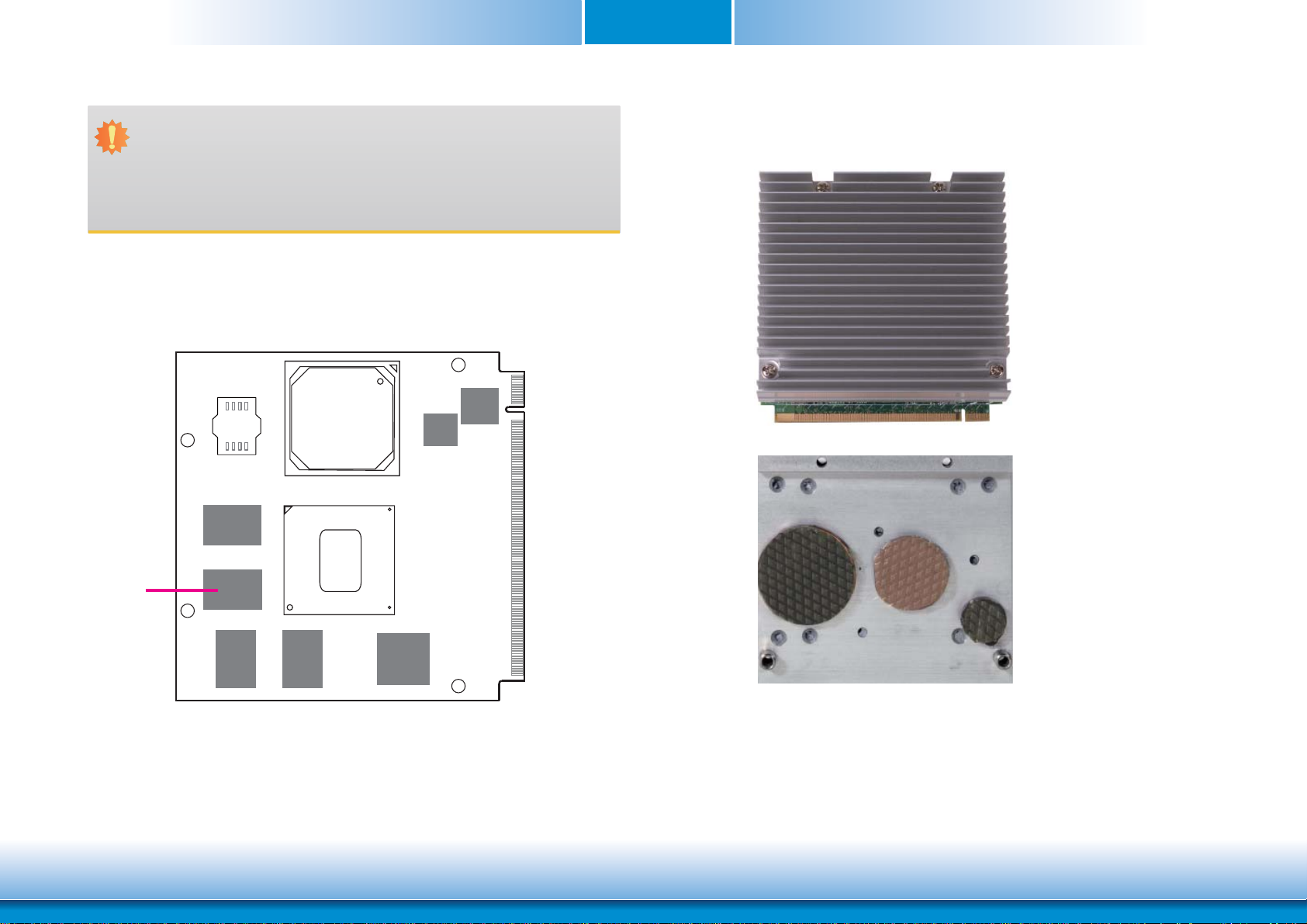
System Memory
The system board is equipped with memory down (single 32-bit channel) that support DDR2.
Cooling Option
Heat Spreader with Heat Sink
Top View of the Heat Sink
1
2
DDR2
3
Bottom View of the Heat Spreader
• “1”, “2” and “3“ denote the locations of
the thermal pads designed to contact
the corresponding components that are
on QB702-B Series.
• Remove the plastic covering from the
thermal pads prior to mounting the heat
sink onto QB702-B Series.
10
www.dfi .comChapter 2 Hardware Installation
Page 11
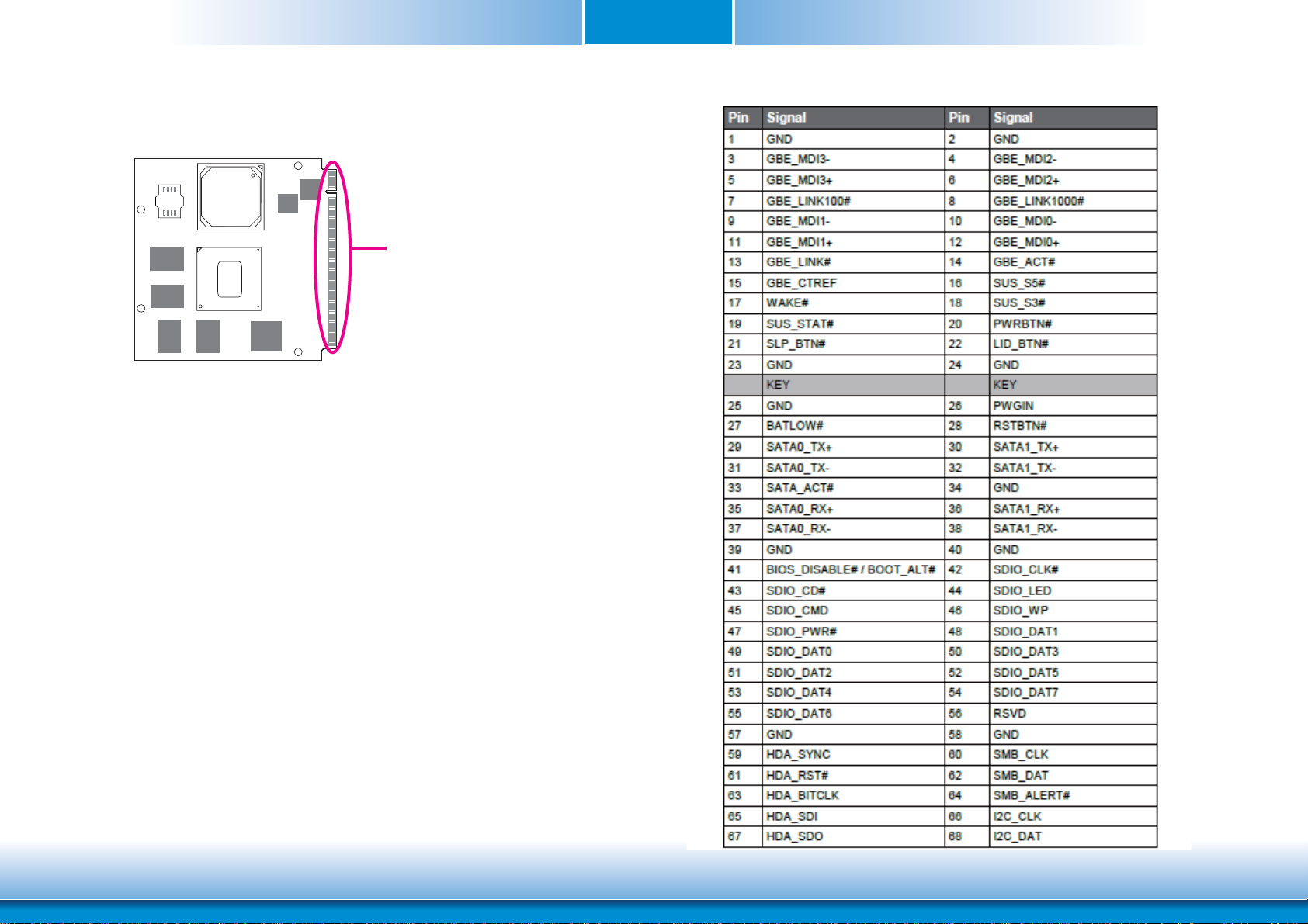
MXM Connector
MXM Connector
The MXM connector is used to interface with the carrier board. Insert QB702-B series to the
MXM connector on the carrier board. Refer to the following page for the pin function of this
connector.
Refer to “Installing QB702-B Series onto a Carrier Board” section for more information.
Chapter 2
11
www.dfi .comChapter 2 Hardware Installation
Page 12
Chapter 2
12
www.dfi .comChapter 2 Hardware Installation
Page 13
Chapter 2
_
_
_
_
_
_
_
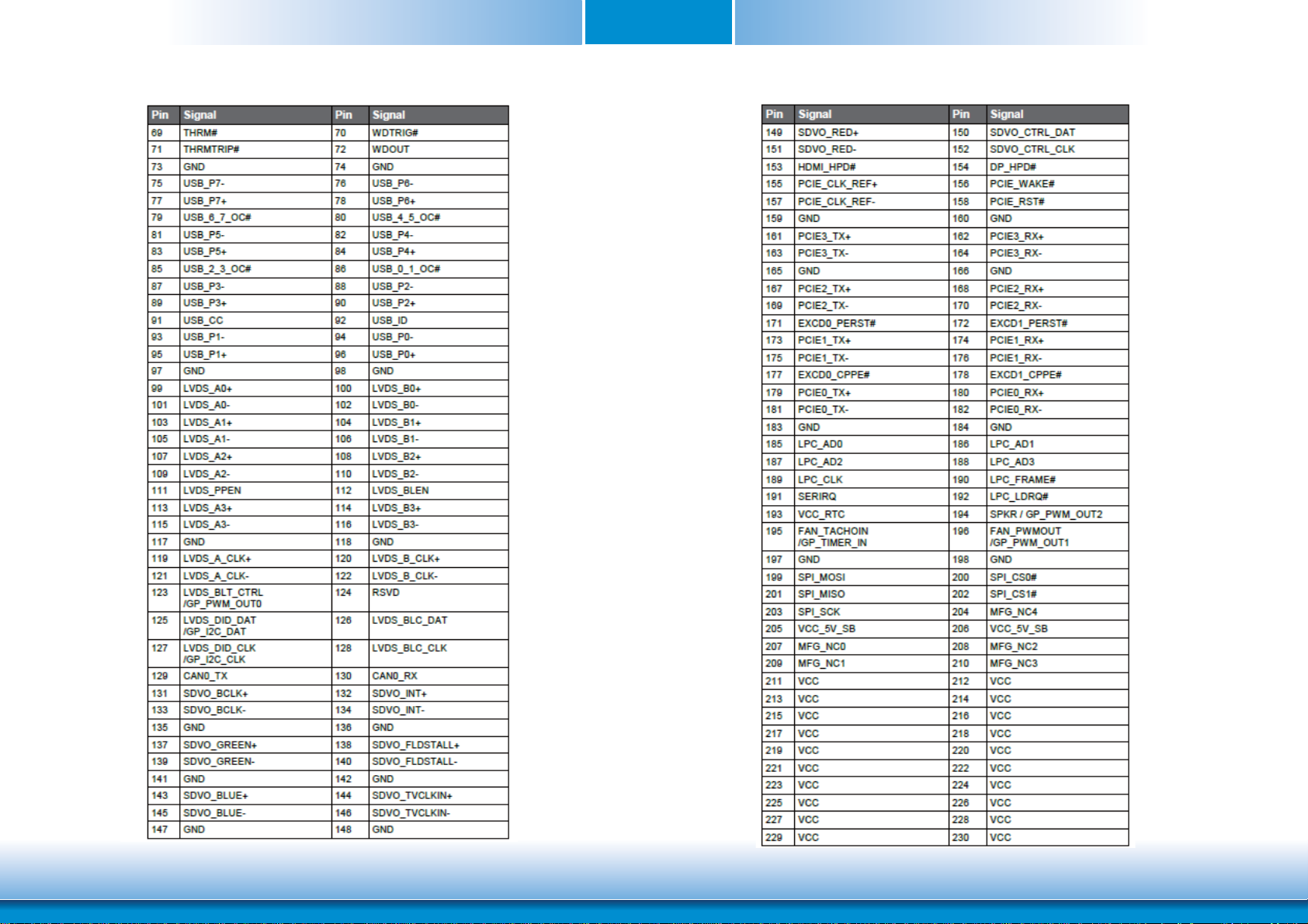
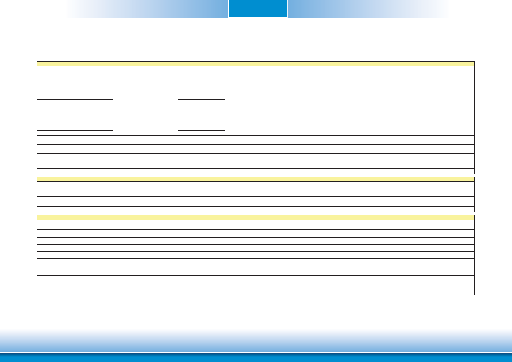
MXM Connector Signal Description
PCI Express Interface Signals Descriptions
Signal Pin# Pin Type Pwr Rail
PCIE0_RX+ 180
PCIE0_RX- 182
PCIE0_TX+
PCIE0_TXPCIE1_RX+ 174
PCIE1_RX- 176
PCIE1_TX+
PCIE1_TXPCIE2_RX+ 168
PCIE2_RX- 170
PCIE2_TX+
PCIE2_TXPCIE3_RX+ 162
PCIE3_RX- 164
PCIE3_TX+
PCIE3_TXPCIE_CLK_REF+ 155
PCIE_CLK_REF- 157
PCIE_WAKE# 156 I CMOS 3.3V Suspend/3.3V PU 10K to 3.3V Suspend PCI Express Wake Event: Sideband wake signal asserted by components requesting wakeup.
PCIE_RST# 158 O CMOS 3.3V/3.3V Reset Signal for external devices.
Express Card Support Pins
Signal Pin# Pin Type Pwr Rail
EXCD0_CPPE# 177 I CMOS 3.3V PU 10K to 3.3V ExpressCard slot #0 capable card request
EXCD0_PERST# 171 O CMOS 3.3V PU 10K to 3.3V ExpressCard slot #0 reset.
EXCD1_CPPE# 178 I CMOS 3.3V PU 10K to 3.3V ExpressCard slot #1 capable card request.
EXCD1_PERST# 172 O CMOS 3.3V ExpressCard slot #1 reset.
Gigabit Ethernet Signals
Signal Pin# Pin Type Pwr Rail
GBE_MDI0+ 12
GBE
MDI0- 10
GBE
MDI1+ 11
MDI1- 9
GBE
MDI2+ 6
GBE
MDI2- 4
GBE
MDI3+ 5
GBE
MDI3- 3
GBE
GBE_CTREF 15 I/O GB_LAN GB_LAN
GBE_LINK# 13 O CMOS 3.3V PP 3.3V/3.3V PU 10K to 2.5V Ethernet controller 0 link indicator, active low.
GBE_LINK100# 7 O CMOS 3.3V PP 3.3V/3.3V Ethernet controller 0 100Mbit/sec link indicator, active low.
GBE_LINK1000# 8 O CMOS 3.3V PP 3.3V/3.3V Ethernet controller 0 1000Mbit/sec link indicator, active low.
GBE_ACT# 14 O CMOS 3.3V PP 3.3V/3.3V PU 10K to 2.5V Ethernet controller 0 activity indicator, active low.
I PCIE
179
O PCUE
181
I PCIE
173
O PCUE
175
I PCIE
167
O PCUE
169
I PCIE
161
O PCUE
163
O PCUE PCIE PCI Express Reference Clock for Lanes 0 to 3.
I/O GB_LAN Media Dependent Interface (MDI) differential pair 0. The MDI can operate in 1000, 100, and 10Mbit/sec modes.This signal pair is used for all modes.
I/O GB_LAN Media Dependent Interface (MDI) differential pair 1. The MDI can operate in 1000, 100, and 10Mbit/sec modes.This signal pair is used for all modes.
I/O GB_LAN Media Dependent Interface (MDI) differential pair 2. The MDI can operate in 1000, 100, and 10Mbit/sec modes.This signal pair is used for all modes.
I/O GB_LAN Media Dependent Interface (MDI) differential pair 3. The MDI can operate in 1000, 100, and 10Mbit/sec modes.This signal pair is used for all modes.
/Tolerance
PCIE
PCIE
PCIE
PCIE
PCIE
PCIE
PCIE
PCIE
/Tolerance
/Tolerance
GB_LAN
GB_LAN
GB_LAN
GB_LAN
PU/PD (DFI-QB702) Description
PCI Express channel 0, Receive Input differential pair.
PCI Express channel 0, Transmit Output differential pair.
PCI Express channel 1, Receive Input differential pair.
PCI Express channel 1, Transmit Output differential pair.
PCI Express channel 2, Receive Input differential pair.
PCI Express channel 2, Transmit Output differential pair.
PCI Express channel 3, Receive Input differential pair.
PCI Express channel 3, Transmit Output differential pair.
PU/PD (DFI-QB702) Description
PU/PD (DFI-QB702) Description
Reference voltage for carrier board Ethernet channel 0 magnetics center tap.
The reference voltage is determined by the requirements of the module's PHY and may be as low as 0V and as high as 3.3V.
The reference voltage output should be current limited on the module. In a case in which the reference is shorted to ground, the current must be limited to 250mA
or less.
13
www.dfi .comChapter 2 Hardware Installation
Page 14
Chapter 2
_
_
_
_
_
_
_
_
_
_
_
_
_
_
_
_
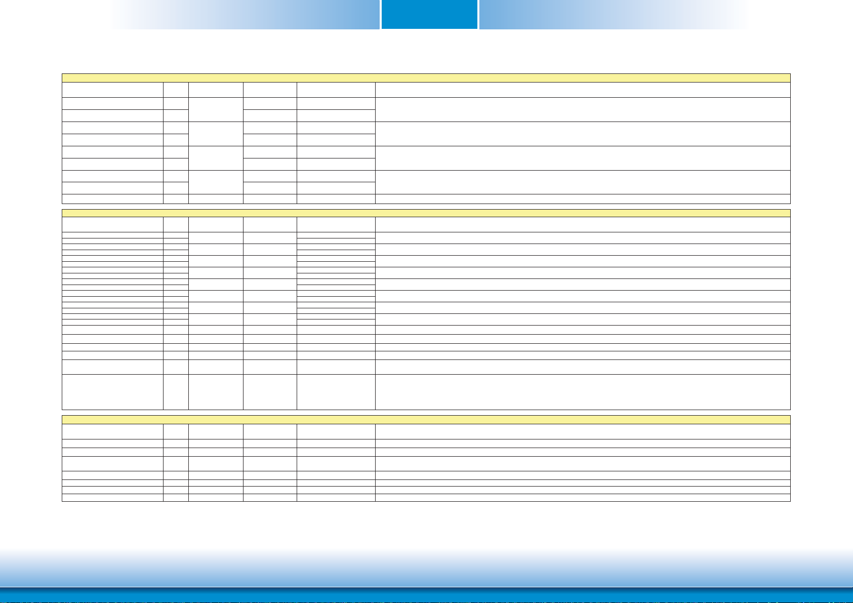
Serial ATA Interface Signals
Signal Pin# Pin Type Pwr Rail
SATA0_RX+ 35
SATA0_RX- 37
SATA0_TX+ 29
SATA0_TX- 31
SATA1_RX+ 36
SATA1_RX- 38
SATA1_TX+ 30
SATA1_TX- 32
SATA_ACT# 33 O OC 3.3V 3.3V/3.3V Serial ATA Led. Open collector output pin driven during SATA command activity.
USB Interface Signals
Signal Pin# Pin Type Pwr Rail
USB
P0+ 96
P0- 94
USB
USB
P1+ 95
P1- 93
USB
P2+ 90
USB
P2- 88
USB
P3+ 89
USB
USB
P3- 87
P4+ 84
USB
P4- 82
USB
P5+ 83
USB
P5- 81
USB
P6+ 78
USB
USB
P6- 76
P7+ 77
USB
P7- 75
USB
USB_0_1_OC# 86 I CMOS 3.3V Suspend/3.3V PU 10K to 3.3V Suspend Over current detect input 1. This pin is used to monitor the USB power over current of the USB Ports 0 and 1.
USB_2_3_OC# 85 I CMOS 3.3V Suspend/3.3V PU 10K to 3.3V Suspend Over current detect input 2. This pin is used to monitor the USB power over current of the USB Ports 2 and 3.
USB_4_5_OC# 80 I CMOS 3.3V Suspend/3.3V PU 10K to 3.3V Suspend Over current detect input 3. This pin is used to monitor the USB power over current of the USB Ports 4 and 5.
USB_6_7_OC# 79 I CMOS 3.3V Suspend/3.3V Not support Over current detect input 4. This pin is used to monitor the USB power over current of the USB Ports 6 and 7.
USB_ID 92 I CMOS 3.3V Suspend/3.3V PD 10K
USB_CC 91 I CMOS 3.3V Suspend/3.3V PD 10K
SDIO Interface Signals
Signal Pin# Pin Type Pwr Rail
SDIO_CD# 43 I/O CMOS 3.3V/3.3V PU 10K to 3.3V SDIO Card Detect. This signal indicates when a SDIO/MMC card is present.
SDIO_CLK 42 O CMOS 3.3V/3.3V SDIO Clock. With each cycle of this signal a one-bit transfer on the command and each data line occurs. This signal has maximum frequency of 48 MHz.
SDIO_CMD 45 I/O OD/PP CMOS 3.3V/3.3V
SDIO_LED 44 O CMOS 3.3V/3.3V SDIO LED. Used to drive an external LED to indicate when transfers occur on the bus.
SDIO_WP 46 I/O CMOS 3.3V/3.3V PU 10K to 3.3V SDIO Write Protect. This signal denotes the state of the write-protect tab on SD cards.
SDIO_PWR# 47 O CMOS 3.3V/3.3V SDIO Power Enable. This signal is used to enable the power being supplied to a SD/MMC card device.
SDIO_DAT0-7 48-55 I/O PP CMOS 3.3V/3.3V SDIO Data lines. These signals operate in push-pull mode
I SATA
O SATA
I SATA
O SATA
I/O USB
I/O USB
I/O USB
I/O USB
I/O USB
I/O USB
I/O USB
/Tolerance
AC coupled on
AC coupled on
AC coupled on
AC coupled on
AC coupled on
AC coupled on
AC coupled on
AC coupled on
/Tolerance
USB
USB
USB
USB
USB
USB
USB
USB
/Tolerance
PU/PD (DFI-QB702) Description
Serial ATA channel 0, Receive Input differential pair.
Serial ATA channel 0, Transmit Output differential pair.
Serial ATA channel 1, Receive Input differential pair.
Serial ATA channel 1, Transmit Output differential pair.
PU/PD (DFI-QB702) Description
Universal Serial Bus Port 0 differential pair.I/O USB
Universal Serial Bus Port 1 differential pair.This port may be optionally used as USB client port.
Universal Serial Bus Port 2 differential pair.
Universal Serial Bus Port 3 differential pair.
Universal Serial Bus Port 4 differential pair.
Universal Serial Bus Port 5 differential pair.
Universal Serial Bus Port 6 differential pair.
Universal Serial Bus Port 7 differential pair.
USB ID pin.Configures the mode of the USB Port 1. If the signal is detected as being 'high active' the BIOS will automatically configure USB Port 1 as USB Client and
enable USB Client support. This signal should be driven as OC signal by external circuitry.
USB Client Connect pin.If USB Port 1 is configured for client mode then an externally connected USB host should set this signal to high-active in order to properly make
the connection with the module's internal USB client controller.
If the external USB host is disconnected, this signal should be set to low-active in order to inform the USB client controller that the external host has been
disconnected.
A level shifter/protection circuitry should be implemented on the carrier board for this signal.
PU/PD (DFI-QB702) Description
SDIO Command/Response. This signal is used for card initialization and for command transfers. During initialization mode this signal is open drain. During command
transfer this signal is in push-pull mode.
14
www.dfi .comChapter 2 Hardware Installation
Page 15
Chapter 2
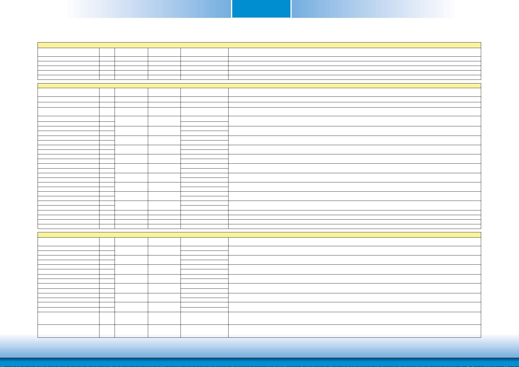
High Definition Audio Signals/AC'97
Signal Pin# Pin Type Pwr Rail
HDA_RST# 61 O CMOS 3.3V/3.3V HD Audio/AC'97 Codec Reset.
HDA_SYNC 59 O CMOS 3.3V/3.3V Serial Bus Synchronization
HDA_BCLK 63 O CMOS 3.3V/3.3V HD Audio/AC'97 24 MHz Serial Bit Clock from Codec.
HDA_SDO 67 O CMOS 3.3V/3.3V HD Audio/AC'97 Serial Data Output to Codec.
HDA_SDIN 65 I CMOS 3.3V/3.3V HD Audio/AC'97 Serial Data input to Codec.
LVDS Flat Panel Signals
Signal Pin# Pin Type Pwr Rail
LVDS_PPEN 111 O CMOS 3.3V/3.3V Controls panel power enable.
LVDS_BLEN 112 O CMOS 3.3V/3.3V Controls panel Backlight enable.
LVDS_BLT_CTRL/GP_PWM_OUT0 123 O CMOS 3.3V/3.3V
LVDS_A0+ 99
LVDS_A0- 101
LVDS_A1+ 103
LVDS_A1- 105
LVDS_A2+ 107
LVDS_A2- 109
LVDS_A3+ 113
LVDS_A3- 115
LVDS_A_CLK+ 119
LVDS_A_CLK- 121
LVDS_B0+ 100
LVDS_B0- 102
LVDS_B1+ 104
LVDS_B1- 106
LVDS_B2+ 108
LVDS_B2- 110
LVDS_B3+ 114
LVDS_B3- 112
LVDS_B_CLK+ 120
LVDS_B_CLK- 122
LVDS_DID_CLK/GP_I2C_CLK 127 I/O OD CMOS 3.3V/3.3V Primary functionality is DisplayID DDC clock line used for LVDS flat panel detection. If primary functionality is not used it can be as General Purpose I²C bus clock line.
LVDS_DID_DAT/GP_I2C_DAT 125 I/O OD CMOS 3.3V/3.3V Primary functionality DisplayID DDC data line used for LVDS flat panel detection. If primary functionality is not used it can be as General Purpose I²C bus data line.
LVDS_BLC_CLK 128 I/O OD CMOS 3.3V/3.3V Control clock signal for external SSC clock chip.
LVDS_BLC_DAT 126 I/O OD CMOS 3.3V/3.3V Control data signal for external SSC clock chip.
SDVO Interface Signals
Signal Pin# Pin Type Pwr Rail
SDVO_BCLK- 133
SDVO_BCLK+ 131
SDVO_INT- 134
SDVO_INT+ 132
SDVO_GREEN- 139
SDVO_GREEN+ 137
SDVO_BLUE- 145
SDVO_BLUE+ 143
SDVO_RED- 151
SDVO_RED+ 149
SDVO_FLDSTALL- 140
SDVO_FLDSTALL+ 138
SDVO_TVCLKIN- 146
SDVO_TVCLKIN+ 144
SDVO_CTRL_CLK 152 I/O OD CMOS 3.3V/3.3V
SDVO_CTRL_DAT 150 I/O OD CMOS 3.3V/3.3V
O LVDS LVDS primary channel differential pair 1.
O LVDS
O LVDS
O LVDS LVDS primary channel differential pair clock lines.
O LVDS LVDS secondary channel differential pair 0.
O LVDS LVDS secondary channel differential pair 1.
O LVDS LVDS secondary channel differential pair 2.
O LVDS
O LVDS LVDS secondary channel differential pair clock lines.
O PCIE
I PCIE
O PCIE
O PCIE
O PCIE
I PCIE
I PCIE
/Tolerance
/Tolerance
LVDS
LVDS
LVDS
LVDS
LVDS
LVDS
LVDS
LVDS
LVDS
LVDS
/Tolerance
SDVO
SDVO
SDVO
SDVO
SDVO
SDVO
SDVO
PU/PD (DFI-QB702) Description
PU/PD (DFI-QB702) Description
Primary functionality is to control the panel backlight brightness via pulse width modulation (PWM).
When not in use for this primary purpose it can be used as General Purpose PWM Output.
LVDS primary channel differential pair 0.O LVDS
LVDS primary channel differential pair 2.
LVDS primary channel differential pair 3.
LVDS secondary channel differential pair 3.
PU/PD (DFI-QB702) Description
SDVO differential pair clock lines.
SDVO differential pair interrupt input lines.
SDVO differential pair green data lines.
SDVO differential pair blue data lines.
SDVO differential pair red data lines.
SDVO differential pair field stall lines.
SDVO differential pair TV-Out synchronization clock lines.
I²C based control signal (clock) for SDVO device.
Note: If the control bus from the SDVO device has a different signaling voltage, then a level shifting device will be required on the carrier board to properly translate
the voltage level for this signal.
I²C based control signal (data) for SDVO device.
Note: If the control bus from the SDVO device has a different signaling voltage, then a level shifting device will be required on the carrier board to properly translate
the voltage level for this signal.
15
www.dfi .comChapter 2 Hardware Installation
Page 16

Chapter 2
HDMI Interface Signals
Signal Pin# Pin Type Pwr Rail
TMDS_CLK- (SDVO_BCLK-) 133
TMDS_CLK+ (SDVO_BCLK+) 131
TMDS_LANE0- (SDVO_BLUE-) 145
TMDS_LANE0+ (SDVO_BLUE+) 143
TMDS_LANE1- (SDVO_GREEN-) 139
TMDS_LANE1+ (SDVO_GREEN+) 137
TMDS_LANE2- (SDVO_RED-) 151
TMDS_LANE2+ (SDVO_RED+) 149
HDMI_CTRL_CLK (SDVO_CTRL_CLK) 152 I/O OD CMOS 3.3V/3.3V
HDMI_CTRL_DAT (SDVO_CTRL_DAT) 150 I/O OD CMOS 3.3V/3.3V
HDMI_HPD# 153 I CMOS 3.3V/3.3V Hot plug detection signal that serves as an interrupt request.
DisplayPort Interface Signals
Signal Pin# Pin Type Pwr Rail
DP_LANE3- (SDVO_BCLK-) 133
DP_LANE3+ (SDVO_BCLK+) 131
DP_LANE2- (SDVO_BLUE-) 145
DP_LANE2+ (SDVO_BLUE+) 143
DP_LANE1- (SDVO_GREEN-) 139
DP_LANE1+ (SDVO_GREEN+) 137
DP_LANE0- (SDVO_RED-) 151
DP_LANE0+ (SDVO_RED+) 149
DP_AUX- (SDVO_FLDSTALL-) 140
DP_AUX+ (SDVO_FLDSTALL+) 138
DP_HPD# 154 I CMOS 3.3V/3.3V Hot plug detection signal that serves as an interrupt request.
LPC Interface Signals
Signal Pin# Pin Type Pwr Rail
LPC_AD[0..3] 185-188 I/O CMOS 3.3V/3.3V Multiplexed Command, Address and Data.
LPC_FRAME# 190 O CMOS 3.3V/3.3V LPC frame indicates the start of a new cycle or the termination of a broken cycle.
LPC_LDRQ# 192 I CMOS 3.3V/3.3V LPC DMA request.
LPC_CLK 189 O CMOS 3.3V/3.3V LPC clock.
SERIRQ 191 I/O CMOS 3.3V/3.3V Serialized Interrupt.
SPI Interface Signals
Signal Pin# Pin Type Pwr Rail
SPI_MOSI 199 O CMOS 3.3V/3.3V Master serial output/Slave serial input signal. SPI serial output data from Qseven module to the SPI device.
SPI_MISO 201 I CMOS 3.3V/3.3V Master serial input/Slave serial output signal. SPI serial input data from the SPI device to Qseven module.
SPI_SCK 203 O CMOS 3.3V/3.3V SPI clock output.
SPI_CS0# 200 O CMOS 3.3V/3.3V SPI chip select 0 output.
SPI_CS1# 202 O CMOS 3.3V/3.3V SPI Chip Select 1 signal is used as the second chip select when two devices are used. Do not use when only one SPI device is used.
CAN Bus Interface Signals
Signal Pin# Pin Type Pwr Rail
CAN0_TX 129 O CMOS 3.3V/3.3V
CAN0_RX 130 I CMOS 3.3V/3.3V PU 10K to 3.3V
O TMDS
O TMDS
O TMDS
O TMDS
O PCIE DisplayPort differential pair lines lane 3.
O PCIE DisplayPort differential pair lines lane 2.
O PCIE DisplayPort differential pair lines lane 1.
O PCIE DisplayPort differential pair lines lane 0.
I/O PCIE Auxiliary channel used for link management and device control. Differential pair lines.
/Tolerance
TMDS
TMDS
TMDS
TMDS
/Tolerance
DP
DP
DP
DP
DP
/Tolerance
/Tolerance
/Tolerance
PU/PD (DFI-QB702) Description
TMDS differential pair clock lines.
TMDS differential pair lines lane 0.
TMDS differential pair lines lane 1.
TMDS differential pair lines lane 2.
DDC based control signal (clock) for HDMI device.
Note: Level shifters must be implemented on the carrier board for this signal in order to be compliant with the HDMI Specification.
DDC based control signal (data) for HDMI device.
Note: Level shifters must be implemented on the carrier board for this signal in order to be compliant with the HDMI Specification
PU/PD (DFI-QB702) Description
PU/PD (DFI-QB702) Description
PU/PD (DFI-QB702) Description
PU/PD (DFI-QB702) Description
CAN (Controller Area Network) TX output for CAN Bus channel 0.
In order to connect a CAN controller device to the Qseven module's CAN bus it is necessary to add transceiver hardware to the carrier board.
RX input for CAN Bus channel 0. In order to connect a CAN controller device to the Qseven module's CAN bus it is necessary to add transceiver hardware to the carrier
board.
16
www.dfi .comChapter 2 Hardware Installation
Page 17

Chapter 2
Power Control Signals
Signal Pin# Pin Type Pwr Rail
PWGIN 26 I CMOS 5V/5V High active input for the Qseven® module indicates that all power rails located on the carrier board are ready for use.
PWRBTN# 20 I CMOS 3.3V Standby Power Button: Low active power button input. This signal is triggered on the falling edge.
Power Management Signals
Signal Pin# Pin Type Pwr Rail
RSTBTN# 28 I CMOS 3.3V/3.3V Reset button input. This input may be driven active low by an external circuitry to reset the Qseven module.
BATLOW# 27 I CMOS 3.3V Suspend/3.3V PU 10K to 3.3V Suspend
WAKE# 17 I CMOS 3.3V Suspend/3.3V PU 10K to 3.3V Suspend External system wake event. This may be driven active low by external circuitry to signal an external wake-up event.
SUS_STAT# 19 O CMOS 3.3V Suspend/3.3V PU 10K to 3.3V Suspend Suspend Status: indicates that the system will be entering a low power state soon.
SUS_S3# 18 O CMOS 3.3V Suspend/3.3V
SUS_S5# 16 O CMOS 3.3V Suspend/3.3V S5 State: This signal indicates S4 or S5 (Soft Off) state.
SLP_BTN# 21 I CMOS 3.3V Suspend/3.3V PU 10K to 3.3V Suspend
LID_BTN# 22 I CMOS 3.3V Suspend/3.3V PU 10K to 3.3V Suspend
Miscellaneous Signals
Signal Pin# Pin Type Pwr Rail
WDTRIG# 70 I CMOS 3.3V/3.3V Watchdog trigger signal. This signal restarts the watchdog timer of the Qseven module on the falling edge of a low active pulse.
WDOUT 72 O CMOS 3.3V/3.3V Watchdog event indicator. High active output used for signaling a missing watchdog trigger. Will be deasserted by software, system reset or a system power down.
I2C_CLK 66 I/O OD CMOS 3.3V/3.3V PU 10K to 3.3V Clock line of I²C bus.
I2C_DAT 68 I/O OD CMOS 3.3V/3.3V PU 10K to 3.3V Data line of I²C bus.
SMB_CLK 60 I/O OD CMOS 3.3V Suspend/3.3V PU 2K to 3.3V Suspend Clock line of System Management Bus.
SMB_DAT 62 I/O OD CMOS 3.3V Suspend/3.3V PU 2K to 3.3V Suspend Data line of System Management Bus.
SMB_ALERT# 64 O CMOS 3.3V/3.3V PU 2K to 3.3V Suspend System Management Bus Alert input. This signal may be driven low by SMB devices to signal an event on the SM Bus.
SPKR/GP_PWM_OUT2 194 O CMOS 3.3V/3.3V
BIOS_DISABLE#/BOOT_ALT# 41 I CMOS 3.3V/3.3V
RSVD 56,124, NC Do not connect
Manufacturing Signals
Signal Pin# Pin Type Pwr Rail
MFG_NC0 207 N.A N.A
MFG_NC1 209 N.A N.A
MFG_NC2 208 N.A N.A
MFG_NC3 210 N.A N.A
MFG_NC4 204 N.A N.A
/Tolerance
/Tolerance
/Tolerance
/Tolerance
PU/PD (DFI-QB702) Description
PU/PD (DFI-QB702) Description
Battery low input. This signal may be driven active low by external circuitry to signal that the system battery is low or may be used to signal some other external
battery management event.
S3 State: This signal shuts off power to all runtime system components that are not maintained during S3 (Suspend to Ram), S4 or S5 states.
The signal SUS_S3# is necessary in order to support the optional S3 cold power state.
Sleep button. Low active signal used by the ACPI operating system to transition the system into sleep state or to wake it up again. This signal is triggered on falling
edge.
LID button. Low active signal used by the ACPI operating system to detect a LID switch and to bring system into sleep state or to wake it up again.
Open/Close state may be software configurable.
PU/PD (DFI-QB702) Description
Primary functionality is output for audio enunciator, the“speaker” in PC AT systems. When not in use for this primary purpose it can be used as General Purpose PWM
Output.
Module BIOS disable input signal. Pull low to disable module's on-board BIOS.
Allows off-module BIOS implementations. This signal can also be used to disable standard boot firmware flash device and enable an alternative boot firmware source, for
example a boot loader.
PU/PD (DFI-QB702) Description
This pin is reserved for manufacturing and debugging purposes.
May be used as JTAG_TCK signal for boundary scan purposes during production or as a vendor specific control signal. When used as a vendor specific control signal the
multiplexer must be controlled by the MFG_NC4 signal.
This pin is reserved for manufacturing and debugging purposes.
May be used as JTAG_TDO signal for boundary scan purposes during production. May also be used, via a multiplexer, as a UART_TX signal to connect a simple UART for
firmware and boot loader implementations. In this case the multiplexer must be controlled by the MFG_NC4 signal.
This pin is reserved for manufacturing and debugging purposes.
May be used as JTAG_TDI signal for boundary scan purposes during production. May also be used, via a multiplexer, as a UART_RX signal to connect a simple UART for
firmware and boot loader implementations. In this case the multiplexer must be controlled by the MFG_NC4 signal.
This pin is reserved for manufacturing and debugging purposes.
May be used as JTAG_TMS signal for boundary scan purposes during production. May also be used, via a multiplexer, as vendor specific BOOT signal for firmware and
boot loader implementations. In this case the multiplexer must be controlled by the MFG_NC4 signal.
This pin is reserved for manufacturing and debugging purposes.
May be used as JTAG_TRST# signal for boundary scan purposes during production. May also be used as control signal for a multiplexer circuit on the module enabling
secondary function for MFG_NC0..3 ( JTAG / UART ).
When MFG_NC4 is high active it is being used for JTAG purposes.
When MFG_NC4 is low active it is being used for UART purposes.
17
www.dfi .comChapter 2 Hardware Installation
Page 18

Chapter 2
Thermal Management Signals
Signal Pin# Pin Type Pwr Rail
THRM# 69 I CMOS 3.3V/3.3V PU 10K to 3.3V Thermal Alarm active low signal generated by the external hardware to indicate an over temperature situation. This signal can be used to initiate thermal throttling.
THRMTRIP# 71 O CMOS 3.3V/3.3V PU 10K to 3.3V Thermal Trip indicates an overheating condition of the processor. If 'THRMTRIP#' goes active the system immediately transitions to the S5 State (Soft Off).
Fan Control Implementation
Signal Pin# Pin Type Pwr Rail
FAN_PWMOUT/GP_PWM_OUT1 196 O CMOS 3.3V/3.3V
FAN_TACHOIN/GP_TIMER_IN 195 I CMOS 3.3V/3.3V Primary functionality is fan tachometer input. When not in use for this primary purpose it can be used as General Purpose Timer Input.
Input Power Pins
Signal Pin# Pin Type Pwr Rail
VCC 211-230 Power Power Supply +5VDC ±5%
VCC_5V_SB 205-206 Power Standby Power Supply +5VDC ±5%
VCC_RTC 193 Power
1-2,
23-25,
34,
39-40,
57-58,
73-74,
GND
97-98,
117-118,
Power Ground Power Ground.
135-136,
141-142,
147-148,
159-160,
165-166,
183-184,
197-198,
/Tolerance
/Tolerance
/Tolerance
PU/PD (DFI-QB702) Description
PU/PD (DFI-QB702) Description
Primary functionality is fan speed control. Uses the Pulse Width Modulation (PWM) technique to control the Fan's RPM based on the CPU's die temperature.
When not in use for this primary purpose it can be used as General Purpose PWM Output.
PU/PD (DFI-QB702) Description
3 V backup cell input. VCC_RTC should be connected to a 3V backup cell for RTC operation and storage register non-volatility in the absence of system power.
(VCC_RTC = 2.4 - 3.3 V).
18
www.dfi .comChapter 2 Hardware Installation
Page 19

Chapter 2
Installing QB702-B Series onto a Carrier Board
Important:
The carrier board used in this section is for reference purpose only and may not
resemble your carrier board. These illustrations are mainly to guide you on how to
install QB702-B Series onto the carrier board of your choice.
1. The photo below shows the locations of the mounting holes and the bolts already fixed in
place.
Standoff Bolts
Mounting hole
3. Press down QB702-B Series and put on the heat sink on top of QB702-B Series with its
mounting holes and bolts aligned on the carrier board. Use the mounting screw to fix
QB702-B Series and heat sink on place.
Short screws
Long screws
2. Grasping QB702-B Series by its edges, insert it into the carrier board, and you will hear a
distinctive¨click¨ indicating QB702-B Series is correctly locked into position.
Carrier board
QB702-B Series
19
www.dfi .comChapter 2 Hardware Installation
Page 20

Chapter 3 - BIOS Setup
Chapter 3
Legends
Overview
The BIOS is a program that takes care of the basic level of communication between the CPU
and peripherals. It contains codes for various advanced features found in this system board.
The BIOS allows you to configure the system and save the configuration in a battery-backed
CMOS so that the data retains even when the power is off. In general, the information stored
in the CMOS RAM of the EEPROM will stay unchanged unless a configuration change has been
made such as a hard drive replaced or a device added.
It is possible that the CMOS battery will fail causing CMOS data loss. If this happens, you need
to install a new CMOS battery and reconfigure the BIOS settings.
Note:
The BIOS is constantly updated to improve the performance of the system board;
therefore the BIOS screens in this chapter may not appear the same as the actual
one. These screens are for reference purpose only.
Default Configuration
Most of the configuration settings are either predefined according to the Load Optimal Defaults
settings which are stored in the BIOS or are automatically detected and configured without
requiring any actions. There are a few settings that you may need to change depending on
your system configuration.
Entering the BIOS Setup Utility
The BIOS Setup Utility can only be operated from the keyboard and all commands are keyboard commands. The commands are available at the right side of each setup screen.
The BIOS Setup Utility does not require an operating system to run. After you power up the
system, the BIOS message appears on the screen and the memory count begins. After the
memory test, the message “Press DEL to run setup” will appear on the screen. If the message
disappears before you respond, restart the system or press the “Reset” button. You may also
restart the system by pressing the <Ctrl> <Alt> and <Del> keys simultaneously.
KEYs Function
Right and Left Arrows Moves the highlight left or right to select a
menu.
Up and Down Arrows Moves the highlight up or down between
submenus or fi elds.
<Esc> Exits to the BIOS setup utility
+ (plus key) Scrolls forward through the values or
options of the hightlighted fi eld.
- (minus key) Scolls backward through the values or
options of the hightlighted fi eld.
Tab Select a fi eld
<F1> Displays general help
<F4> Saves and exits the setup program
<Enter> Press <Enter> to enter the highlighted
submenu
Scroll Bar
When a scroll bar appears to the right of the setup screen, it indicates that there are more
available fields not shown on the screen. Use the up and down arrow keys to scroll through all
the available fields.
Submenu
When ““ appears on the left of a particular field, it indicates that a submenu which contains
additional options are available for that field. To display the submenu, move the highlight to
that field and press <Enter>.
20
www.dfi .comChapter 3 BIOS Setup
Page 21

Chapter 3
AMI BIOS Setup Utility
Main
The Main menu is the first screen that you will see when you enter the BIOS Setup Utility.
Main
BIOS Information
BIOS Vendor
Core Version
Project Version
Build Date
Memory Information
MRC Version
Total Memory
System Date
System Time
Access Level
System Date
The date format is <day>, <month>, <date>, <year>. Day displays a day, from Sunday to Saturday. Month displays the month, from January to December. Date displays
the date, from 1 to 31. Year displays the year, from 1980 to 2099.
System Time
Aptio Setup Utility - Copyright (C) 2011 American Megatrends, Inc.
Advanced
Version 2.14.1219. Copyright (C) 2011 American Megatrends, Inc.
Boot Security
American Megatrends
4.6.3.7
OABTN 0.32
12/18/2012 14:19:08
01.00
1024 MB (DDR2)
[Thu 01/01/2009]
[18:36:56]
Administraor
Save & ExitChipset
Set the Date. Use TAB
to switch between Data
elements.
Select Screen
Select Item
Enter: Select
+/-: Change Opt.
F1: General Help
F2: Previous Values
F3: Optimized Defaults
F4: Save & Exit
ESC: Exit
Advanced
The Advanced menu allows you to configure your system for basic operation. Some entries are
defaults required by the system board, while others, if enabled, will improve the performance
of your system or let you set some features according to your preference.
Important:
Setting incorrect field values may cause the system to malfunction.
Main
Legacy OpROM Support
Launch PXE OpROM [Disabled]
Launch Storage OpROM [Enabled]
APCI Settings
CPU Confi guration
SDIO Confi guration
USB Confi guration
Module Board H/W Monitor
Launch Storage OpROM
Enable or Disable Boot Option for Legacy Mass Storage Devices with Option ROM.
Aptio Setup Utility - Copyright (C) 2011 American Megatrends, Inc.
Advanced
Version 2.14.1219. Copyright (C) 2011 American Megatrends, Inc.
Save & ExitChipset Boot Security
Enable or Disable Boot
Option for Legacy Network Devices.
Select Screen
Select Item
Enter: Select
+/-: Change Opt.
F1: General Help
F2: Previous Values
F3: Optimized Defaults
F4: Save & Exit
ESC: Exit
The time format is <hour>, <minute>, <second>. The time is based on the 24-hour
military-time clock. For example, 1 p.m. is 13:00:00. Hour displays hours from 00 to
23. Minute displays minutes from 00 to 59. Second displays seconds from 00 to 59.
21
www.dfi .comChapter 3 BIOS Setup
Page 22

Chapter 3
ACPI Settings
This section is used to configure the ACPI Settings.
Aptio Setup Utility - Copyright (C) 2011 American Megatrends, Inc.
Advanced
ACPI Sleep State
Version 2.14.1219. Copyright (C) 2011 American Megatrends, Inc.
[S3 (Suspend to RAM) ]
Select the highest ACPI
sleep state the system will
enter, when the SUSPEND
button is pressed.
Select Screen
Select Item
Enter: Select
+/-: Change Opt.
F1: General Help
F2: Previous Values
F3: Optimized Defaults
F4: Save & Exit
ESC: Exit
ACPI Sleep State
Select the highest ACPI sleep state the system will enter when the SUSPEND button is
pressed.
S3(STR) Enables the Suspend to RAM function.
CPU Configuration
This section is used to configure the CPU. It will also display the detected CPU
information.
Aptio Setup Utility - Copyright (C) 2011 American Megatrends, Inc.
Advanced
CPU Confi guration
Processor Type
EMT64
Processor Speed
System Bus Speed
Ratio Status
Actual Ratio
System Bus Speed
Processor Stepping
Microcode Revision
L1 Cache RAM
L2 Cache RAM
Processor Core
Hyper-Threading
Intel SpeedStep
Hyper-Threading
Execute Disable Bit
Limit CPUID Maximum
Intel Virtualization Technology
Version 2.14.1219. Copyright (C) 2011 American Megatrends, Inc.
Intel (R) Atom (TM) CPU
Supported
1300 MHz
400 MHz
13
13
400 MHz
20661
261
56 k
512 k
Single
Supported
[Enabled]
[Enabled]
[Enabled]
[Disabled]
[Disabled]
Enable or Disable Intel
(R) SpeedStep (tm)
Select Screen
Select Item
Enter: Select
+/-: Change Opt.
F1: General Help
F2: Previous Values
F3: Optimized Defaults
F4: Save & Exit
ESC: Exit
Hyper-Threading
Enabled for Windows XP and Linux (OS optimized for Hyper-Threading Technology)
and Disabled for other OS (OS not optimized for Hyper-Threading Technology)
Execute Disable Bit
XD can prevent certain classes of malicious buffer overflow attacks when combined
with a supporting OS (Windows Server 2003 SP1, Windows XP sp2, SuSE Linux 9.2,
RedHat Enterprise 3 update 3.)
.
Limit CPUID Maximum
Disabled for Windows XP.
Intel Virtualization Technology
When enabled, a VMM can utilize the additional hardware capabilities provided by
vanderpool Technology.
22
www.dfi .comChapter 3 BIOS Setup
Page 23

Chapter 3
SDIO Configuration
This section configures settings relevant to SDIO.
Aptio Setup Utility - Copyright (C) 2011 American Megatrends, Inc.
Advanced
SDIO Confi guration
SDIO Access Mode
Version 2.14.1219. Copyright (C) 2011 American Megatrends, Inc.
[Auto]
Auto Option: Access SD
device in DMA mode
if controller supports it,
otherwise in PIO mode.
DMA Option: Access SD
device in DMA mode. PIO
Option: Access SD device
in PIO mode.
Select Screen
Select Item
Enter: Select
+/-: Change Opt.
F1: General Help
F2: Previous Values
F3: Optimized Defaults
F4: Save & Exit
ESC: Exit
USB Configuration
This section is used to configure USB.
Aptio Setup Utility - Copyright (C) 2011 American Megatrends, Inc.
Advanced
USB Confi guation
USB Devices:
1 keyboard, 1 Hub
Legacy USB Support
EHCI Hand-off
Version 2.14.1219. Copyright (C) 2011 American Megatrends, Inc.
[Enabled]
[Disabled]
Enables Legacy USB
Support. AUTO option
disables
Select Screen
Select Item
Enter: Select
+/-: Change Opt.
F1: General Help
F2: Previous Values
F3: Optimized Defaults
F4: Save & Exit
ESC: Exit
EHCI Hand-off
This is a workaround for OSes without EHCI hand-off support. The EHCI
ownership change should be claimed by EHCI driver.
23
www.dfi .comChapter 3 BIOS Setup
Page 24

Chapter 3
Module Board H/W Monitor
This section is used to configure Module Board H/W Monitor.
Aptio Setup Utility - Copyright (C) 2011 American Megatrends, Inc.
Advanced
=== Module Board H/W Monitor ===
Current CPU Temperature
System FAN1 Speed
Vcore
VGFX
+3.3 (V)
+1.8 (V)
Fan1 Mode Setting
Fan1 Manual Value
Version 2.14.1219. Copyright (C) 2011 American Megatrends, Inc.
: +39.750 C
: N/A
: +1.014 V
: +0.926 V
: +3.288 V
: +1.854 V
[Manual Mode]
255
Confi gure Fan Mode.
Select Screen
Select Item
Enter: Select
+/-: Change Opt.
F1: General Help
F2: Previous Values
F3: Optimized Defaults
F4: Save & Exit
ESC: Exit
Fan1 Manual Value
Fan Manual Value Setting Min=0, Max=255. Please input Dec Number:
Chipset
Configures relevant chipset functions.
Main
North Bridge Chipset Confi guration
South Bridge Chipset Confi guration
Aptio Setup Utility - Copyright (C) 2011 American Megatrends, Inc.
Advanced
Chipset
Version 2.14.1219. Copyright (C) 2011 American Megatrends, Inc.
Boot Security
Save & Exit
North Bridge Parameters
Select Screen
Select Item
Enter: Select
+/-: Change Opt.
F1: General Help
F2: Previous Values
F3: Optimized Defaults
F4: Save & Exit
ESC: Exit
24
www.dfi .comChapter 3 BIOS Setup
Page 25

Chapter 3
North Bridge Chipset Configuration
Main
North Bridge Chipset Confi guration
Memory Information
MRC Version
Total Memory
vBIOS Version
IGD Mode Select
Aptio Setup Utility - Copyright (C) 2011 American Megatrends, Inc.
Advanced
Chipset
Version 2.14.1219. Copyright (C) 2011 American Megatrends, Inc.
Boot Security
01.00
1024 MB (DDR2)
2032
[Enabled, 8MB]
Save & Exit
Select the amount of
system memeory used by
the Integrated Graphics
Cards.
Select Screen
Select Item
Enter: Select
+/-: Change Opt.
F1: General Help
F2: Previous Values
F3: Optimized Defaults
F4: Save & Exit
ESC: Exit
South Bridge Chipset Configuration
Aptio Setup Utility - Copyright (C) 2011 American Megatrends, Inc.
Chipset
South Bridge Chipset Confi guration
Audio Confi guration
PCI Express Ports Confi guration
Version 2.14.1219. Copyright (C) 2011 American Megatrends, Inc.
[Auto]
Audio Controller options.
Select Screen
Select Item
Enter: Select
+/-: Change Opt.
F1: General Help
F2: Previous Values
F3: Optimized Defaults
F4: Save & Exit
ESC: Exit
25
www.dfi .comChapter 3 BIOS Setup
Page 26

Chapter 3
PCI Express Ports Configuration
Aptio Setup Utility - Copyright (C) 2011 American Megatrends, Inc.
Chipset
PCI Express Ports Confi guration
PCI Express Root Ports 0
PCI Express Root Ports 1
PCI Express Root Ports 2
PCI Express Root Ports 3
Version 2.14.1219. Copyright (C) 2011 American Megatrends, Inc.
PCI Express Root Port 0
Settings.
Select Screen
Select Item
Enter: Select
+/-: Change Opt.
F1: General Help
F2: Previous Values
F3: Optimized Defaults
F4: Save & Exit
ESC: Exit
PCI Express Root Ports 0
Aptio Setup Utility - Copyright (C) 2011 American Megatrends, Inc.
PCI Express Root Ports 0
Version 2.14.1219. Copyright (C) 2011 American Megatrends, Inc.
Chipset
[Enable]
PCI Express Root Port 0
Settings.
Select Screen
Select Item
Enter: Select
+/-: Change Opt.
F1: General Help
F2: Previous Values
F3: Optimized Defaults
F4: Save & Exit
ESC: Exit
26
www.dfi .comChapter 3 BIOS Setup
Page 27

Chapter 3
PCI Express Root Ports 1~3
Aptio Setup Utility - Copyright (C) 2011 American Megatrends, Inc.
Chipset
PCI Express Root Ports 1
Version 2.14.1219. Copyright (C) 2011 American Megatrends, Inc.
PCI Express Root Port 0
Settings.
Select Screen
Select Item
Enter: Select
+/-: Change Opt.
F1: General Help
F2: Previous Values
F3: Optimized Defaults
F4: Save & Exit
ESC: Exit
Boot
Main
Boot Confi guration
Quiet Boot
Setup Prompt Timeout
Bootup NumLock State
CSM16 Module Version
Boot Option Priorities
Aptio Setup Utility - Copyright (C) 2011 American Megatrends, Inc.
Advanced
Version 2.14.1219. Copyright (C) 2011 American Megatrends, Inc.
Boot
[Disabled]
1
[On]
07.65
Security
Save & ExitChipset
Enables/Disables Quiet
Boot Option.
Select Screen
Select Item
Enter: Select
+/-: Change Opt.
F1: General Help
F2: Previous Values
F3: Optimized Defaults
F4: Save & Exit
ESC: Exit
Setup Prompt Timeout
Number of seconds to wait for setup activation key. 65535(0xFFFF) means indefinite
waiting.
Bootup NumLock State
Select the keyboard NumLock state.
27
www.dfi .comChapter 3 BIOS Setup
Page 28

Chapter 3
Security
Main
Password Description
If ONLY the Administrator’s password is set,
then this only limits access to Setup and is only
asked for when entering Setup.
If ONLY the User’s password is set, then this
is a power on password and must be entered to
boot or enter Setup. In Setup the User will have
Administrator rights.
Administrator Password
User Password
Administrator Password
Sets the administrator password.
User Password
Sets the user password.
Aptio Setup Utility - Copyright (C) 2011 American Megatrends, Inc.
Advanced
Version 2.14.1219. Copyright (C) 2011 American Megatrends, Inc.
Boot Security
Save & Exit
Save & ExitChipset
Set Setup Administrator
Password.
Select Screen
Select Item
Enter: Select
+/-: Change Opt.
F1: General Help
F2: Previous Values
F3: Optimized Defaults
F4: Save & Exit
ESC: Exit
Main
Save Changes and Reset
Discard Changes and Reset
Restore Defaults
Save as User Defaults
Restore User Defaults
Boot Override
Launch EFI Shell from fi lesystem device
Discard Changes and Reset
Reset system setup without saving any changes.
Restore Defaults
Restore/Load Defaults values for all the setup options.
Save as User Defaults
Aptio Setup Utility - Copyright (C) 2011 American Megatrends, Inc.
Advanced
Chipset
Version 2.14.1219. Copyright (C) 2011 American Megatrends, Inc.
Boot Security Save & Exit
Reset the system after
saving the changes.
Select Screen
Select Item
Enter: Select
+/-: Change Opt.
F1: General Help
F2: Previous Values
F3: Optimized Defaults
F4: Save & Exit
ESC: Exit
Save the changes done so far as User Defaults.
Restore User Defaults
Restore the User Defaults to all the setup options.
Launch EFI Shell from filesystem device
Attempts to Launch EFI Shell application (Shell. efi) from one of the available
filesystem device.
28
www.dfi .comChapter 3 BIOS Setup
Page 29

Updating the BIOS
To update the BIOS, you will need the new BIOS file and a flash utility, AFU238.EXE.
Please contact technical support or your sales representative for the files.
To execute the utility, type:
A:> AFU238 BIOS_File_Name /b /p /n
then press <Enter>.
C:\AFU\AFU238>afu238 fi lename /b /p /n
+--------------------------------------------------------------------------------------------------------+
|
|
+--------------------------------------------------------------------------------------------------------+
Reading fi le ..............................
Erasing fl ash .............................
Writing fl ash .............................
Verifying fl ash ..........................
Erasing BootBlock ....................
Writing BootBlock ....................
Verifying BootBlock .................
C:\AFU\AFU238>
AMI Firmware Update Utility(APTIO) v2.25
Copyright (C)2011 American Megatrends Inc. All Rights Reserved.
done
done
done
done
done
done
done
|
|
Chapter 3
After finishing BIOS update, please turn off the AC power. Wait about 10 seconds and then
turn on the AC power again.
29
www.dfi .comChapter 3 BIOS Setup
Page 30

Chapter 4 - Supported Software
The CD that came with the system board contains drivers, utilities and software applications
required to enhance the performance of the system board.
Insert the CD into a CD-ROM drive. The autorun screen (Mainboard Utility CD) will appear. If
after inserting the CD, “Autorun” did not automatically start (which is, the Mainboard Utility
CD screen did not appear), please go directly to the root directory of the CD and double-click
“Setup”.
Chapter 4
Microsoft .NET Framework 3.5 SP1
Note:
Before installing Microsoft .NET Framework 3.5 SP1, make sure you have updated
your Windows XP operating system to Service Pack 3.
To install the driver, click “Microsoft .NET Framework 3.5 SP1” on the main menu.
1. Read the license agreement
carefully.
Click “I have read and accept
the terms of the License Agreement” then click Install.
2. Setup is now installing the driver.
30
www.dfi .comChapter 4 Supported Software
Page 31

Chapter 4
3. Click Exit.
Intel Chipset Software Installation Utility
The Intel Chipset Software Installation Utility is used for updating Windows® INF files so that
the Intel chipset can be recognized and configured properly in the system.
To install the utility, click “Intel Chipset Software Installation Utility” on the main menu.
1. Setup is ready to install the
utility. Click Next.
2. Read the license agreement
then click Yes.
31
www.dfi .comChapter 4 Supported Software
Page 32

Chapter 4
3. Go through the readme document for more installation tips
then click Next.
4. After all setup operations are
done, click Next.
Microsoft DirectX 9.0C Driver
To install the utility, click “Microsoft DirectX 9.0C Driver” on the main menu.
1. Click “I accept the agrment”
then click Next.
2. To start installation, click
Next.
5. Click “Yes, I want to restart this
computer now” then click Finish.
Restarting the system will allow the
new software installation to take
effect.
3. Click Finish. Reboot the
system for DirectX to take
effect.
32
www.dfi .comChapter 4 Supported Software
Page 33

Chapter 4
Intel Graphics Drivers
To install the driver, click “Intel Embedded Media and Graphics Drivers” on the main menu.
Note:
Before installing Intel Graphics Drivers, make sure you have installed Microsoft .NET
Framework 3.5 SP1.
1. Setup is now ready to install the
graphics driver. Click on “Installs
driver and application files”, then
click on Next.
2. Read the license agreement carefully.
Click “I agree“ then click Install.
4. Setup is now installing the driver.
5. Click on “Continue Anyway“.
6. Click “Yes” to restart this computer
now.
Restarting the system will allow the
new software installlation to take
effect.
3. Click on “Continue Anyway“.
33
www.dfi .comChapter 4 Supported Software
Page 34

Chapter 4
Audio Drivers (for Q7-100 Carrier Board)
To install the driver, click “Audio Drivers” on the main menu.
1. Setup is now ready to install the
audio driver. Click Next.
2. Follow the remainder of the steps
on the screen; clicking “Next”
each time you finish a step.
3. Click “Yes, I want to restart my
computer now” then click Finish.
Restarting the system will allow the
new software installation to take
effect.
Intel Platform Controller Hub EG20T Drivers
To install the driver, click “Intel Platform Controller Hub EG20t Drivers” on the main menu.
1. Setup is now preparing to
install the driver.
2. Setup is now ready to install
the driver. Click Next.
3. Click “I accept the terms in
the license agreement” then
click “Next”.
34
www.dfi .comChapter 4 Supported Software
Page 35

Chapter 4
4. Click Next.
5. Click Install to begin installation.
7. Click Continue Anyway or
Stop Installation.
8. Click Finish to exit installation.
6. Wait until the driver is being
installed, then click Next.
35
www.dfi .comChapter 4 Supported Software
Page 36

Chapter 4
DFI Utility
DFI Utility provides information about the board, HW Health, Watchdog, DIO, and Backlight. To
access the utility, click “DFI Utility” on the main menu.
1. Setup is ready to install the DFI
Utility drifer. Click Next.
2. Click “I accept the terms in the
license agreement” and then click
.
Next
3. Enter “User Name” and “Organization” information and then click
.
Next
4. Click Install to begin the installation.
5. After completing installation,
click Finish.
36
www.dfi .comChapter 4 Supported Software
Page 37

Chapter 4
The DFI Utility icon will appear on the desktop. Double-click the icon to open the utility.
F6 Floppy
This is used to create a floppy driver diskette needed when you install Windows® XP using
the F6 installation method. This will allow you to install the operating system onto a hard drive
when in AHCI mode.
1. Insert a blank floppy diskette.
2. Locate for the drivers in the CD then copy them to the floppy diskette. The CD includes
drivers for both 32-bit and 64-bit operating systems. The path to the drivers are shown
below.
32-bit
CD Drive:\AHCI_RAID\F6FLOPPY\f6flpy32
37
www.dfi .comChapter 4 Supported Software
Page 38

Adobe Acrobat Reader 9.3
To install the reader, click “Adobe Acrobat Reader 9.3” on the main menu.
1. Click Next to install or click
Change Destination Folder to
select another folder.
2. Click Install to begin installation.
Chapter 4
3. Click Finish to exit installation.
38
www.dfi .comChapter 4 Supported Software
Page 39

Appendix A
Appendix A - NLITE and AHCI Installation Guide
nLite
nLite is an application program that allows you to customize your XP installation disc by
integrating the RAID/AHCI drivers into the disc. By using nLite, the F6 function key usually
required during installation is no longer needed.
Note:
The installation steps below are based on nLite version 1.4.9. Installation procedures
may slightly vary if you’re using another version of the program.
1. Download the program from nLite’s offical website.
http://www.nliteos.com/download.html
2. Install nLite.
4. Insert the XP installation disc
into an optical drive.
5. Launch nLite. The Welcome
screen will appear. Click
Next.
Important:
Due to it’s coding with Visual.Net, you may need to first install .NET Framework prior
to installing nLite.
3. Download relevant RAID/AHCI driver files from Intel’s website. The drivers you choose will
depend on the operating system and chipset used by your computer.
The downloaded driver files
should include iaahci.cat,
iaAHCI.inf, iastor.cat, iaStor.
inf, IaStor.sys, license.txt and
TXTSETUP.OEM.
6. Click Next to temporarily
save the Windows installation files to the designated
default folder.
If you want to save them in
another folder, click Browse,
select the folder and then click
Next.
39
www.dfi .comAppendix A NLITE and AHCI Installation Guide
Page 40

Appendix A
7. Click Next.
8. In the Task Selection dialog
box, click Drivers and
Bootable ISO. Click Next.
9. Click Insert and then select
Multiple driver folder to
select the drivers you will
integrate. Click Next.
10. Select only the drivers ap-
propriate for the Windows
version that you are using
and then click OK.
Integrating 64-bit drivers into
32-bit Windows or vice versa
will cause file load errors and
failed installation.
40
www.dfi .comAppendix A NLITE and AHCI Installation Guide
Page 41

Appendix A
11. If you are uncertain of the
southbridge chip used on
your motherboard, select all
RAID/AHCI controllers and
then click OK
12. Click Next.
.
13. The program is currently
integrating the drivers and
applying changes to the
installation.
14. When the program is finished applying the changes,
click Next.
41
www.dfi .comAppendix A NLITE and AHCI Installation Guide
Page 42

Appendix A
15. To create an image, select the
Create Image mode under the
General section and then click
Next.
16. Or you can choose to burn it
directly to a disc by selecting
the Direct Burn mode under
the General section.
Select the optical device and all
other necessary settings and then
click Next
.
17. You have finished customizing
the Windows XP installation disc.
Click Finish.
Enter the BIOS utility to configure
the SATA controller to RAID/AHCI.
You can now install Windows XP.
42
www.dfi .comAppendix A NLITE and AHCI Installation Guide
Page 43

Appendix A
AHCI
The installation steps below will guide you in configuring your SATA drive to AHCI
mode.
1. Enter the BIOS utility and configure the SATA controller to IDE mode.
2. Install Windows XP but do not press F6.
3. Download relevant RAID/AHCI driver files supported by the motherboard chipset from Intel’s website.
Transfer the downloaded driver
files to C:\AHCI.
4. Open Device Manager and
right click on one of the
Intel Serial ATA Storage Controllers, then select Update
Driver.
If the controller you selected
did not work, try selecting
another one.
5. In the Hardware Update Wizard
dialog box, select “No, not this
time” then click Next.
6. Select “Install from a list or
specific location (Advanced)” and
then click Next.
7. Select “Don’t search. I will choose
the driver to install” and then click
.
Next
43
www.dfi .comAppendix A NLITE and AHCI Installation Guide
Page 44

Appendix A
8. Click “Have Disk”.
9. Select C:\AHCI\iaAHCI.inf
and then click Open.
11. A warning message appeared
because the selected SATA
controller did not match your
hardware device.
Ignore the warning and click Yes to
proceed.
12. Click Finish.
13. The system’s settings have
been changed. Windows XP
requires that you restart the
computer. Click Yes.
10. Select the appropriate AHCI
Controller of your hardware
device and then click Next.
14. Enter the BIOS utility and
modify the SATA controller
from IDE to AHCI. By doing
so, Windows will work normally
with the SATA controller that is
in AHCI mode.
44
www.dfi .comAppendix A NLITE and AHCI Installation Guide
Page 45

Appendix B
Appendix B - System Error Message
When the BIOS encounters an error that requires the user to correct something, either a beep
code will sound or a message will be displayed in a box in the middle of the screen and the
message, PRESS F1 TO CONTINUE, CTRL-ALT-ESC or DEL TO ENTER SETUP, will be shown in
the information box at the bottom. Enter Setup to correct the error.
Error Messages
One or more of the following messages may be displayed if the BIOS detects an error during
the POST. This list indicates the error messages for all Awards BIOSes:
CMOS BATTERY HAS FAILED
The CMOS battery is no longer functional. It should be replaced.
Important:
Danger of explosion if battery incorrectly replaced. Replace only with the same or
equivalent type recommended by the manufacturer. Dispose of used batteries according to the battery manufacturer’s instructions.
CMOS CHECKSUM ERROR
Checksum of CMOS is incorrect. This can indicate that CMOS has become corrupt. This error
may have been caused by a weak battery. Check the battery and replace if necessary.
DISPLAY SWITCH IS SET INCORRECTLY
The display switch on the motherboard can be set to either monochrome or color. This indicates the switch is set to a different setting than indicated in Setup. Determine which setting
is correct, either turn off the system and change the jumper or enter Setup and change the
VIDEO selection.
45
www.dfi .comAppendix B System Error Message
Page 46

Appendix C - Troubleshooting
Appendix C
The picture seems to be constantly moving.
Troubleshooting Checklist
This chapter of the manual is designed to help you with problems that you may encounter
with your personal computer. To efficiently troubleshoot your system, treat each problem individually. This is to ensure an accurate diagnosis of the problem in case a problem has multiple
causes.
Some of the most common things to check when you encounter problems while using your
system are listed below.
1. The power switch of each peripheral device is turned on.
2. All cables and power cords are tightly connected.
3. The electrical outlet to which your peripheral devices are connected is working. Test the
outlet by plugging in a lamp or other electrical device.
4. The monitor is turned on.
5. The display’s brightness and contrast controls are adjusted properly.
6. All add-in boards in the expansion slots are seated securely.
7. Any add-in board you have installed is designed for your system and is set up correctly.
Monitor/Display
If the display screen remains dark after the system is turned on:
1. Make sure that the monitor’s power switch is on.
2. Check that one end of the monitor’s power cord is properly attached to the monitor and the
other end is plugged into a working AC outlet. If necessary, try another outlet.
1. The monitor has lost its vertical sync. Adjust the monitor’s vertical sync.
2. Move away any objects, such as another monitor or fan, that may be creating a magnetic
field around the display.
3. Make sure your video card’s output frequencies are supported by this monitor.
The screen seems to be constantly wavering.
1. If the monitor is close to another monitor, the adjacent monitor may need to be turned off.
Fluorescent lights adjacent to the monitor may also cause screen wavering.
Power Supply
When the computer is turned on, nothing happens.
1. Check that one end of the AC power cord is plugged into a live outlet and the other end
properly plugged into the back of the system.
2. Make sure that the voltage selection switch on the back panel is set for the correct type of
voltage you are using.
3. The power cord may have a “short” or “open”. Inspect the cord and install a new one if
necessary.
3. Check that the video input cable is properly attached to the monitor and the system’s
display adapter.
4. Adjust the brightness of the display by turning the monitor’s brightness control knob
.
46
www.dfi .comAppendix C Troubleshooting
Page 47

Appendix C
Hard Drive
Hard disk failure.
1. Make sure the correct drive type for the hard disk drive has been entered in the BIOS.
2. If the system is configured with two hard drives, make sure the bootable (first) hard drive
is configured as Master and the second hard drive is configured as Slave. The master hard
drive must have an active/bootable partition.
Excessively long formatting period.
If your hard drive takes an excessively long period of time to format, it is likely a cable connection problem. However, if your hard drive has a large capacity, it will take a longer time to
format.
Serial Port
The serial device (modem, printer) doesn’t output anything or is outputting garbled
characters.
1. Make sure that the serial device’s power is turned on and that the device is on-line.
2. Verify that the device is plugged into the correct serial port on the rear of the computer.
3. Verify that the attached serial device works by attaching it to a serial port that is working and configured correctly. If the serial device does not work, either the cable or the serial
device has a problem. If the serial device works, the problem may be due to the onboard I/O
or the address setting.
4. Make sure the COM settings and I/O address are configured correctly.
System Board
1. Make sure the add-in card is seated securely in the expansion slot. If the add-in card is
loose, power off the system, re-install the card and power up the system.
2. Check the jumper settings to ensure that the jumpers are properly set.
3. Verify that all memory modules are seated securely into the memory sockets.
4. Make sure the memory modules are in the correct locations.
5. If the board fails to function, place the board on a flat surface and seat all socketed compo-
nents. Gently press each component into the socket.
6. If you made changes to the BIOS settings, re-enter setup and load the BIOS defaults.
Keyboard
Nothing happens when a key on the keyboard was pressed.
1. Make sure the keyboard is properly connected.
2. Make sure there are no objects resting on the keyboard and that no keys are pressed during the booting process.
47
www.dfi .comAppendix C Troubleshooting
 Loading...