

Page 1

NB80-EA
Rev. A+
System Board
User’s Manual
935-NB8001-000
63700243
Page 2

Copyright
This publication contains information that is protected by copyright.
No part of it may be reproduced in any form or by any means or
used to make any transformation/adaptation without the prior
written permission from the copyright holders.
This publication is provided for informational purposes only. The
manufacturer makes no representations or warranties with respect to
the contents or use of this manual and specifically disclaims any
express or implied warranties of merchantability or fitness for any
particular purpose. The user will assume the entire risk of the use or
the results of the use of this document. Further, the manufacturer
reserves the right to revise this publication and make changes to its
contents at any time, without obligation to notify any person or
entity of such revisions or changes.
© 2002. All Rights Reserved.
Trademarks
Windows® 98 SE, Windows® ME, Windows® 2000, Windows NT
4.0 and Windows® XP are registered trademarks of Microsoft
Corporation. Intel® and Pentium® 4 are registered trademarks of
Intel Corporation. Award is a registered trademark of Award
Software, Inc. Other trademarks and registered trademarks of
products appearing in this manual are the properties of their
respective holders.
Caution
To avoid damage to the system:
• Use the correct AC input voltage range
To reduce the risk of electric shock:
• Unplug the power cord before removing the system chassis
cover for installation or servicing. After installation or servicing,
cover the system chassis before plugging the power cord.
..
.
..
®
Page 3

Battery:
• Danger of explosion if battery incorrectly replaced.
• Replace only with the same or equivalent type recommend
the manufacturer.
• Dispose of used batteries according to the battery
manufacturer’s
Joystick or MIDI port:
• Do not use any joystick or MIDI device that requires more than
10A current at 5V DC. There is a risk of fire for devices that
exceed this limit.
instructions.
FCC and DOC Statement on Class B
This equipment has been tested and found to comply with the limits
for a Class B digital device, pursuant to Part 15 of the FCC rules.
These limits are designed to provide reasonable protection against
harmful interference when the equipment is operated in a residential
installation. This equipment generates, uses and can radiate radio
frequency energy and, if not installed and used in accordance with
the instruction manual, may cause harmful interference to radio
communications. However, there is no guarantee that interference
will not occur in a particular installation. If this equipment does cause
harmful interference to radio or television reception, which can be
determined by turning the equipment off and on, the user is
encouraged to try to correct the interference by one or more of the
following measures:
by
• Reorient or relocate the receiving antenna.
• Increase the separation between the equipment and the receiver.
• Connect the equipment into an outlet on a circuit different from
that to which the receiver is connected.
• Consult the dealer or an experienced radio TV technician for
help.
Notice:
1. The changes or modifications not expressly approved by the
party responsible for compliance could void the user's authority
to operate the equipment.
2. Shielded interface cables must be used in order to comply with
the emission limits.
Page 4

Notice
This user’s manual contains detailed information about the system
board. If, in some cases, some information doesn’t match those
shown in the multilingual manual, the multilingual manual should
always be regarded as the most updated version. The multilingual
manual is included in the system board package.
To view the user’s manual, inser t the CD into a CD-ROM drive. The
autorun screen (Mainboard Utility CD) will appear. Click the “Tools”
icon then click “Manual” on the main menu.
Page 5

Table of Contents
Chapter 1 - Introduction
1.1 Features and Specifications..................................................................................
1.2 Hyper-Threading Technology Functionality Requirements..........
1.3 Package Checklist.........................................................................................................
Chapter 2 - Hardware Installation
2.1 System Board Layout ..........................................................................................
2.2 System Memory...........................................................................................................
2.3 Jumper Settings for Clearing CMOS Data........................................
2.4 Jumper Settings for Wake-On-Keyboard/Mouse..................................
2.5 Jumper Settings for Wake-On-USB Keyboard.......................................
2.6 Jumper Settings for Selecting the CPU’s Front Side Bus......
2.7 Jumper Settings for USB 6................................................................................
2.8 Jumper Settings for Serial ATA......................................................................
2.9 Jumper Settings for Serial ATA’s Master/Slave Select...............
2.10 Jumper Settings for RAID...................................................................................
2.11 Factory Use Jumper.................................................................................................
2.12 Rear Panel I/O Ports..............................................................................................
2.13 I/O Connectors...........................................................................................................
Chapter 3 - Award BIOS Setup Utility
3.1 The Basic Input/Output System.....................................................................
3.1.1 Standard CMOS Features.............................................................
3.1.2 Advanced BIOS Features..............................................................
3.1.3 Advanced Chipset Features ......................................................
3.1.4 Integrated Peripherals.........................................................................
3.1.5 Power Management Setup............................................................
3.1.6 PnP/PCI Configurations....................................................................
3.1.7 PC Health Status...................................................................................
3.1.8 Frequency/Voltage Control............................................................
3.1.9 Load Fail-Safe Defaults.....................................................................
3.1.10 Load Optimized Defaults..............................................................
3.1.11 Set Supervisor Password...............................................................
3.1.12 Set User Password..............................................................................
7
15
15
16
17
21
23
25
27
28
29
30
31
32
33
42
66
66
72
77
80
90
94
96
98
100
100
101
101
Page 6

1
Introduction
3.1.13 Save & Exit Setup.................................................................................
3.1.14 Exit Without Saving..............................................................................
3.2 Updating the BIOS.....................................................................................................
Chapter 4 - Supported Softwares
4.1 Desktop Management Interface......................................................................
4.2 Drivers, Utilities and Software Applications..........................................
4.3 Installation Notes...........................................................................................................
Appendix A - Enabling Hyper-Threading
Technology
A.1 Enabling Hyper-Threading Technology..........................................................
Appendix B - System Error Messages
B.1 POST Beep.......................................................................................................................
B.2 Error Messages..............................................................................................................
Appendix C - Troubleshooting
C.1 Troubleshooting Checklist....................................................................................
102
102
103
105
108
119
120
123
123
125
6
Page 7

Introduction
Chapter 1 - Introduction
1.1 Features and Specifications
1.1.1 Features
Chipset
• Intel® E7205 chipset
- Intel® E7205 Memory Controller Hub (MCH)
- Intel® 82801DB I/O Controller Hub (ICH4)
Processor
The system board is equipped with Socket 478 for installing one of
the following supported processors.
• Intel® Pentium® 4 Processor with Hyper-Threading Technology
(Refer to section 1.2 for the Hyper-Threading Technology
functionality requirements)
• Intel® Pentium® 4 processor (478-pin)
- 533MHz system data bus
- 400MHz system data bus
• Intel® Celeron® processor (478-pin)
- 400MHz system data bus
1
System Memory
• Supports single and/or dual channel (144-bit wide) PC2100
(DDR266) memory interface
• Supports up to 4GB system memory
• Supports non-ECC (x64) or ECC (x72) PC2100 (DDR266)
DIMM using 128Mb, 256Mb or 512Mb
Density
Density Width
Single/Double
184-pin DDR
X8
SS/DS
64/128MB
64 Mbit
X16
SS/DS
32MB/NA
128 Mbit
X8
SS/DS
128/256MB
X16
SS/DS
64MB/NA
256 Mbit
X8
SS/DS
256/512MB
X16
SS/DS
128MB/NA
512 Mbit
X8
SS/DS
512/1024MB
X16
SS/DS
256MB/NA
7
Page 8

1
Introduction
Expansion Slots
The system board is equipped with 1 AGP slot, 5 PCI slots (1
shared with CNR slot) and 1 CNR slot.
Note:
PCI slot 5 supports Slave mode only.
AGP (Accelerated Graphics Port)
• Supports 1.5V AGP 8x (2.13GB/sec bandwidth) and AGP 4x
(1066MB/sec. bandwidth) add-in cards. 3.3V AGP card is not
supported.
• Supports AGP 3.0 and AGP 2.0 spec.
AGP is an interface designed to support high performance 3D
graphics cards for 3D graphics applications. It handles large
amounts of graphics data with the following features:
• Pipelined memor y read and write operations that hide
memory access latency.
• Demultiplexing of address and data on the bus for nearly
100 percent efficiency.
CNR (Communication and Networking Riser)
CNR (Communication and Networking Riser) is an interface that
supports multi-channel audio, V.90 analog modem, phone-line based
networking or 10/100 Ethernet based networking riser board.
Onboard Audio Features
• 20-bit stereo full-duplex codec with independent variable
sampling rate
• High quality differential CD input
• True stereo line level outputs
• S/PDIF-in/out interface
• 6-channel audio output
8
Page 9

Introduction
Onboard LAN Features
• Uses Realtek RTL8100 fast ethernet controller
• Integrated IEEE 802.3, 10BASE-T and 100BASE-TX compatible
PHY
• 32-bit PCI master interface
• Integrated power management functions
• Full duplex support at both 10 and 100 Mbps
• Supports IEEE 802.3u auto-negotiation
• Supports wire for management
Integrated Media Reader Interfaces - Smart I/O
• Supports Security Application Smart Card interface
• Supports two most promising compact storage - Memory Stick
interface and Secure Digital Memory Card interface
Compatibility
• PCI 2.2, CNR 1.0 “A” type and AC ’97 compliant
• Intel AGP version 3.0
ATA RAID
1
• RAID 0 (striping) or RAID 1 (mirroring) - RAID 0 and RAID 1
cannot coexist
• Two independent IDE channels support up to 4 drives (UDMA
modes 33/66/100 or EIDE)
• Supports PIO modes 0/1/2/3/4, DMA modes 0/1/2 and
UDMA modes 0/1/2/3/4/5
SATA (Serial ATA) IDE Interface
• Supports one SATA (Serial ATA) interface which is compliant with
SATA 1.0 specification
PCI Bus Master IDE Controller
• Two PCI IDE interfaces support up to four IDE devices
• Supports ATA/33, ATA/66 and ATA/100 hard drives
• PIO Mode 4 Enhanced IDE (data transfer rate up to 14MB/sec.)
• Bus mastering reduces CPU utilization during disk transfer
• Supports ATAPI CD-ROM, LS-120 and ZIP
9
Page 10

1
Introduction
IrDA Interface
The system board is equipped with an IrDA connector for wireless
connectivity between your computer and peripheral devices.
USB Ports
The system board supports USB 2.0 and USB 1.1 ports. USB 1.1
supports 12Mb/second bandwidth while USB 2.0 supports 480Mb/
second bandwidth providing a marked improvement in device
transfer speeds between your computer and a wide range of
simultaneously accessible external Plug and Play peripherals.
BIOS
• Award BIOS, Windows® 98SE/2000/ME/XP Plug and Play
compatible
• Supports SCSI sequential boot-up
• Flash EPROM for easy BIOS upgrades
• Supports DMI 2.0 function
Desktop Management Interface (DMI)
The system board comes with a DMI 2.0 built into the BIOS. The
DMI utility in the BIOS automatically records various information
about your system configuration and stores these information in the
DMI pool, which is a part of the system board's Plug and Play
BIOS. DMI, along with the appropriately networked software, is
designed to make inventory, maintenance and troubleshooting of
computer systems easier. Refer to chapter 4 for instructions on using
the DMI utility.
10
Rear Panel I/O Ports (PC 99 color-coded connectors)
• 4 USB 2.0/1.1 ports
• 1 RJ45 LAN port
• 2 NS16C550A-compatible DB-9 serial ports
• 1 DB-25 parallel port
• 1 mini-DIN-6 PS/2 mouse port
• 1 mini-DIN-6 PS/2 keyboard port
• 3 audio jacks: line-out, line-in and mic-in
Page 11

Introduction
I/O Connectors
• 1 connector for 2 additional external USB 2.0/1.1 ports
• 1 connector for external line-out and mic-in jacks
• 1 connector for an external game/MIDI port
• 2 internal audio connectors (CD-in and TAD)
• 1 4-channel audio output connector
• 1 S/PDIF-in connector
• 1 S/PDIF-out connector
• 1 connector for IrDA interface
• 1 Serial ATA connector
• 2 RAID IDE connectors
• 2 IDE connectors
• 1 floppy drive interface supports up to two 2.88MB floppy
drives
• 2 ATX power supply connectors
• 1 Wake-On-LAN connector
• 1 Wake-On-Ring connector
• CPU fan, chassis fan and system fan fan connectors
• 1 Smart Card interface
• 1 Memory Stick / Secure Digital Memory Card interface
1
1.1.2 System Health Monitor Functions
The system board is capable of monitoring the following “system
health” conditions.
• Monitors CPU/system temperature and overheat alarm
• Monitors Vcore/5VSB/VBAT/3.3V/5V/12V voltages and failure
alarm
• Monitors the fan speed of CPU fan and system fan; and failure
alarm
• Automatic system fan on/off control
• Read back capability that displays temperature, voltage and fan
speed
Refer to the “PC Health Status” section in chapter 3 and the
“Hardware Monitor” section in chapter 4 for more information.
11
Page 12

1
Introduction
1.1.3 Intelligence
Automatic System Fan Off
The system fan will automatically turn off once the system enters the
Suspend mode.
Dual Function Power Button
Depending on the setting in the “Soft-Off By PWR-BTTN” field of
the Power Management Setup, this switch will allow the system to
enter the Soft-Off or Suspend mode.
Wake-On-Ring
This feature allows the system that is in the Suspend mode or Soft
Power Off mode to wake-up/power-on to respond to calls coming
through an internal or external modem. Refer to “Wake-On-Ring
Connector” in chapter 2 and “Resume On Ring” in the Power
Management Setup section in chapter 3 for more information.
Important:
If you are using a modem add-in card, the 5VSB power source
of your power supply must support ≥720mA.
12
Wake-On-LAN
The Wake-On-LAN function is applicable only when you are using a
LAN add-in card that has the same function. It allows the network
to remotely wake up a Soft Power Down (Soft-Off) PC. Your LAN
card must support the remote wakeup function. Refer to “Wake-OnLAN Connector” in chapter 2 and “Resume On LAN” in the Power
Management Setup section in chapter 3 for more information.
Important:
The 5VSB power source of your power supply must support
≥
720mA.
Page 13

Introduction
Wake-On-Keyboard/Wake-On-Mouse
This function allows you to use the keyboard or PS/2 mouse to
power-on the system. Refer to “Jumper Settings for Wake-OnKeyboard/Wake-On-Mouse” in chapter 2 and “Keyboard/Mouse
Power On” (“Onboard Super IO Device” field) in the Integrated
Peripherals section in chapter 3 for more information.
Important:
• The power button will not function once a keyboard
password has been set in the “KB Power On Password”
field of the Integrated Peripherals submenu. You must type
the correct password to power-on the system. If you forgot
the password, power-off the system and remove the
battery. Wait for a few seconds and install it back before
powering-on the system.
• The 5VSB power source of your power supply must
support ≥720mA.
Wake-On-USB Keyboard
The Wake-On-USB Keyboard function allows you to use a USB
keyboard to wake up a system from the S3 (STR - Suspend To
RAM) state. Refer to “Jumper Settings for Wake-On-USB Keyboard”
in chapter 2 and “USB KB Wake-Up From S3” in the Power
Management Setup section in chapter 3 for more information.
1
Important:
• If you are using the Wake-On-USB Keyboard function for 2
USB ports, the 5VSB power source of your power supply
must support ≥1.5A.
• If you are using the Wake-On-USB Keyboard function for 3
or more USB ports, the 5VSB power source of your power
supply must support ≥2A.
RTC Timer to Power-on the System
The RTC installed on the system board allows your system to
automatically power-on on the set date and time. Refer to “Resume
By Alarm” in the Power Management Setup section in chapter 3 for
more information.
13
Page 14

1
Introduction
ACPI STR
The system board is designed to meet the ACPI (Advanced
Configuration and Power Interface) specification. ACPI has energy
saving features that enables PCs to implement Power Management
and Plug-and-Play with operating systems that support OS Direct
Power Management. Currently, only Windows
supports the ACPI function. ACPI when enabled in the Power
Management Setup will allow you to use the Suspend to RAM
function.
With the Suspend to RAM function enabled, you can power-off the
system at once by pressing the power button or selecting “Standby”
when you shut down Windows
to go through the sometimes tiresome process of closing files,
applications and operating system. This is because the system is
capable of storing all programs and data files during the entire
operating session into RAM (Random Access Memory) when it
powers-off. The operating session will resume exactly where you left
off the next time you power-on the system.
Important:
The 5VSB power source of your power supply must support
≥
1A.
®®
®
®®
98SE/2000/ME/XP without having
®®
®
®®
98SE/2000/ME/XP
14
AC Power Failure Recovery
When power returns after an AC power failure, you may choose to
either power-on the system manually, let the system power-on
automatically or return to the state where you left off before power
failure occurs. Refer to “PWR Lost Resume State” (“Onboard Super
IO Device”) in the Integrated Peripherals section in chapter 3 for
more information.
Virus Protection
Most viruses today destroy data stored in hard drives. The system
board is designed to protect the boot sector and partition table of
your hard disk drive.
Page 15

Introduction
1.2 Hyper-Threading Technology Functionality
Requirements
Enabling the functionality of Hyper-Threading Technology for your
computer system requires ALL of the following platforms.
Components:
• CPU - an Intel® Pentium® 4 Processor with HT Technology
• Chipset - an Intel® chipset that supports HT Technology
• BIOS - a BIOS that supports HT Technology and has it enabled
• OS - an operating system that includes optimizations for HT
Technology
Please refer to Appendix A for information about enabling the
functionality of the Hyper-Threading Technology. For more information
on Hyper-Threading Technology, go to: www.intel.com/info/
hyperthreading.
1.3 Package Checklist
The system board package contains the following items:
1
; The system board
; A user’s manual
; One card-edge bracket mounted with a game/MIDI port
; One card-edge bracket mounted with 1 S/PDIF-in connector
and 1 S/PDIF-out connector (optional)
; One IDE cable for ATA/33, ATA/66 or ATA/100 IDE drives
; One 34-pin floppy disk drive cable
; One “Main Board Utility” CD
If any of these items are missing or damaged, please contact your
dealer or sales representative for assistance.
15
Page 16
2
Hardware Installation
Chapter 2 - Hardware Installation
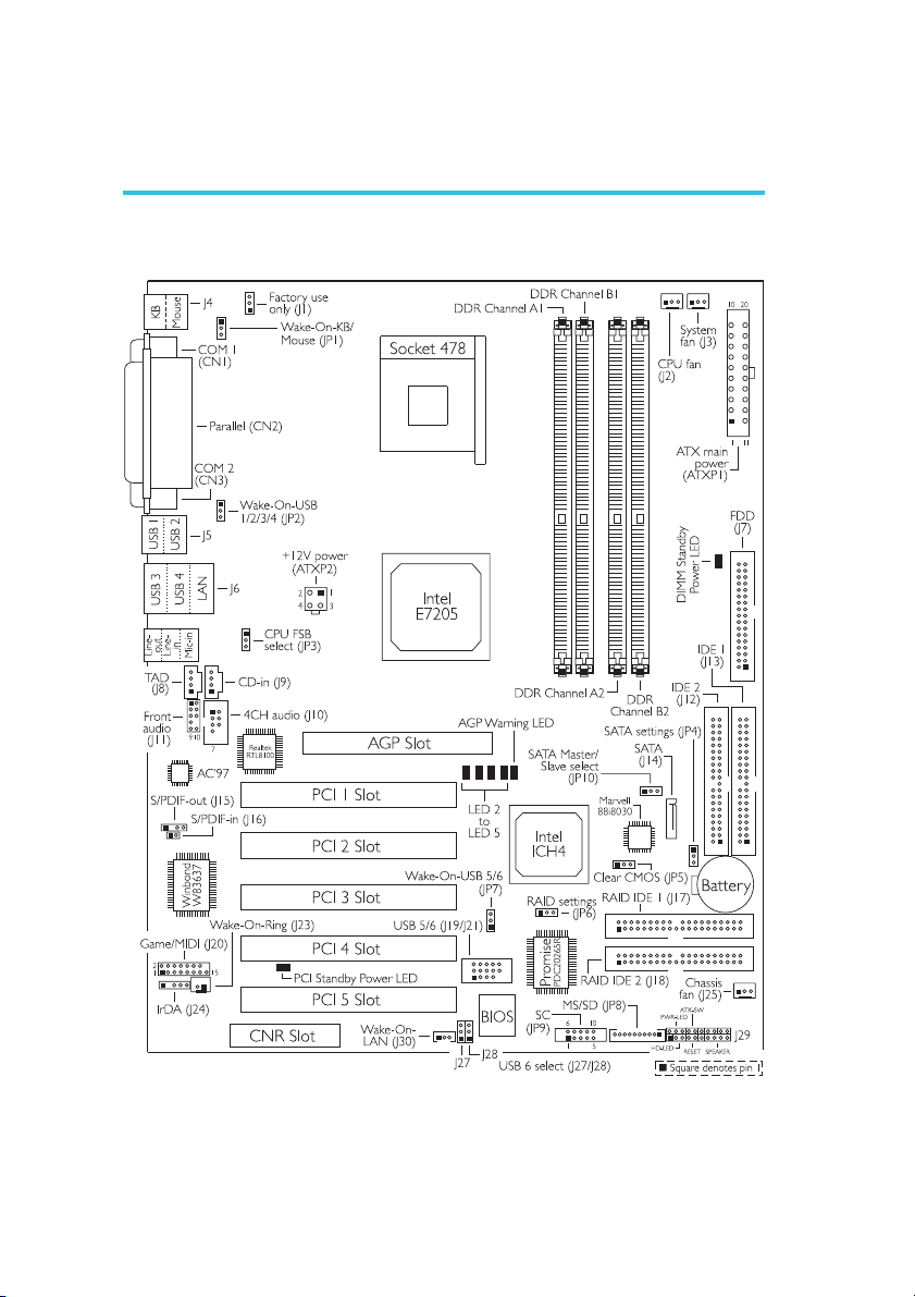
2.1 System Board Layout
16
Page 17
Hardware Installation
Warning:
Electrostatic discharge (ESD) can damage your system board,
processor, disk drives, add-in boards, and other components. Perform
the upgrade instruction procedures described at an ESD workstation
only. If such a station is not available, you can provide some ESD
protection by wearing an antistatic wrist strap and attaching it to a
metal part of the system chassis. If a wrist strap is unavailable,
establish and maintain contact with the system chassis throughout
any procedures requiring ESD protection.
2.2 System Memory
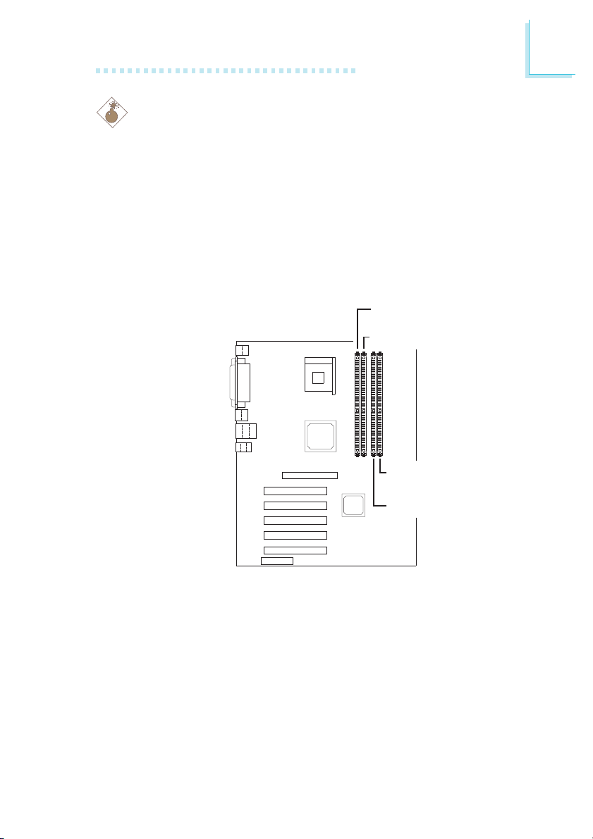
DDR
Channel A1
DDR
Channel B1
DDR
Channel B2
DDR
Channel A2
2
The system board supports DDR SDRAM DIMM. Double Data
Rate SDRAM (DDR SDRAM) is a type of SDRAM that doubles the
data rate through reading and writing at both the rising and falling
edge of each clock. This effectively doubles the speed of operation
therefore doubling the speed of data transfer.
The four DDR DIMM sockets on the system board are divided into 2
channels:
Channel A - sockets A1 and A2
Channel B - sockets B1 and B2
17
Page 18

2
Hardware Installation
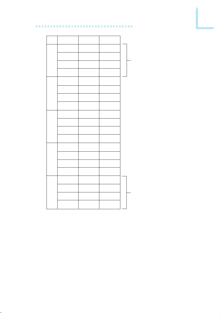
The system board supports single and/or dual channel DDR memory
interface. Inserting DIMMs on the same channel (e.g. A1 and A2 or
B1 and B2) provides single channel memory interface while DIMMs
inserted on different channels (e.g. A1 and B1 or A2 and B2) will
provide dual channel memory interface. Refer to the following tables
for the recommended configurations and their corresponding channel
type.
1
2
3
4
5
Sockets
A1
B1
A2
B2
A1
B1
A2
B2
A1
B1
A2
B2
A1
B1
A2
B2
A1
B1
A2
B2
DIMM
9
9
9
9
9
9
9
9
9
9
9
Channel
Single
Single
Dual
Dual
Dual
18
Page 19
Hardware Installation
2
6
7
8
9
10
Sockets
A1
B1
A2
B2
A1
B1
A2
B2
A1
B1
A2
B2
A1
B1
A2
B2
A1
B1
A2
B2
DIMM
9
9
9
9
9
9
9
9
9
9
9
Channel
Single
This configuration will only
show A1 and A2’s DIMM
size.
NA
NA
Single
Single
This configuration will only
show B1 and B2’s DIMM
size.
19
Page 20
2
Hardware Installation
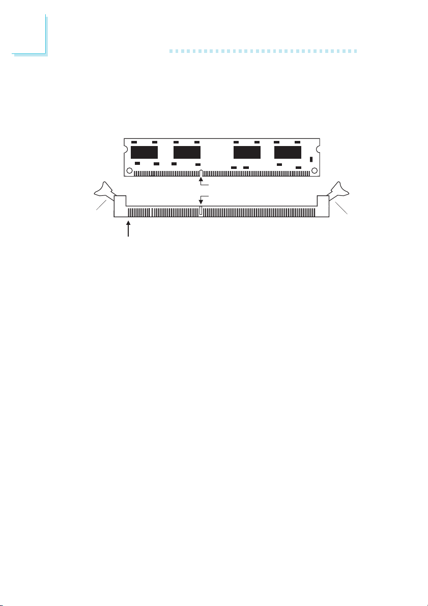
2.2.1 Installing the DIM Module
A DIM module simply snaps into a DIMM socket on the system
board. Pin 1 of the DIM module must correspond with Pin 1 of the
socket.
Notch
Key
Tab
Pin 1
1. Pull the “tabs” which are at the ends of the socket to the side.
2. Position the DIMM above the socket with the “notch” in the
module aligned with the “key” on the socket.
3. Seat the module vertically into the socket. Make sure it is
completely seated. The tabs will hold the DIMM in place.
Tab
20
Page 21
Hardware Installation
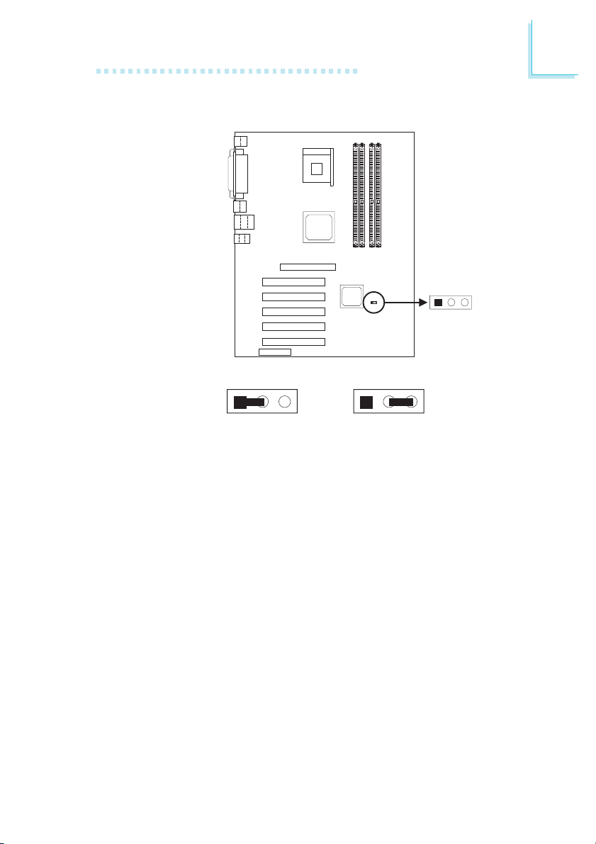
2.3 Jumper Settings for Clearing CMOS Data
3
12
Clear CMOS
(JP5)
123 12 3
2
1-2 On: Normal
(default)
Clear CMOS Data - Jumper JP5
If you encounter the following,
a) CMOS data becomes corrupted.
b) You forgot the supervisor or user password.
c) You are unable to boot-up the computer system because the
processor’s ratio/clock was incorrectly set in the BIOS.
you can reconfigure the system with the default values stored in the
ROM BIOS.
To load the default values stored in the ROM BIOS, please follow
the steps below.
1. Power-off the system.
2. Set JP5 pins 2 and 3 to On. Wait for a few seconds and set JP5
back to its default setting, pins 1 and 2 On.
2-3 On:
Clear CMOS Data
21
Page 22

2
Hardware Installation
3. Now power-on the system.
If your reason for clearing the CMOS data is due to incorrect
setting of the processor’s ratio/clock in the BIOS, please proceed
to step 4.
4. After powering-on the system, press <Del> to enter the main
menu of the BIOS.
5. Select the Frequency/Voltage Control submenu and press
<Enter>.
6. Set the “CPU Clock Ratio” or “Clock By Slight Adjust” field to its
default setting or an appropriate frequency ratio or bus clock.
Refer to the Frequency/Voltage Control section in chapter 3 for
more information.
7. Press <Esc> to return to the main menu of the BIOS setup
utility. Select “Save & Exit Setup” and press <Enter>.
8. Type <Y> and press <Enter>.
22
Page 23
Hardware Installation
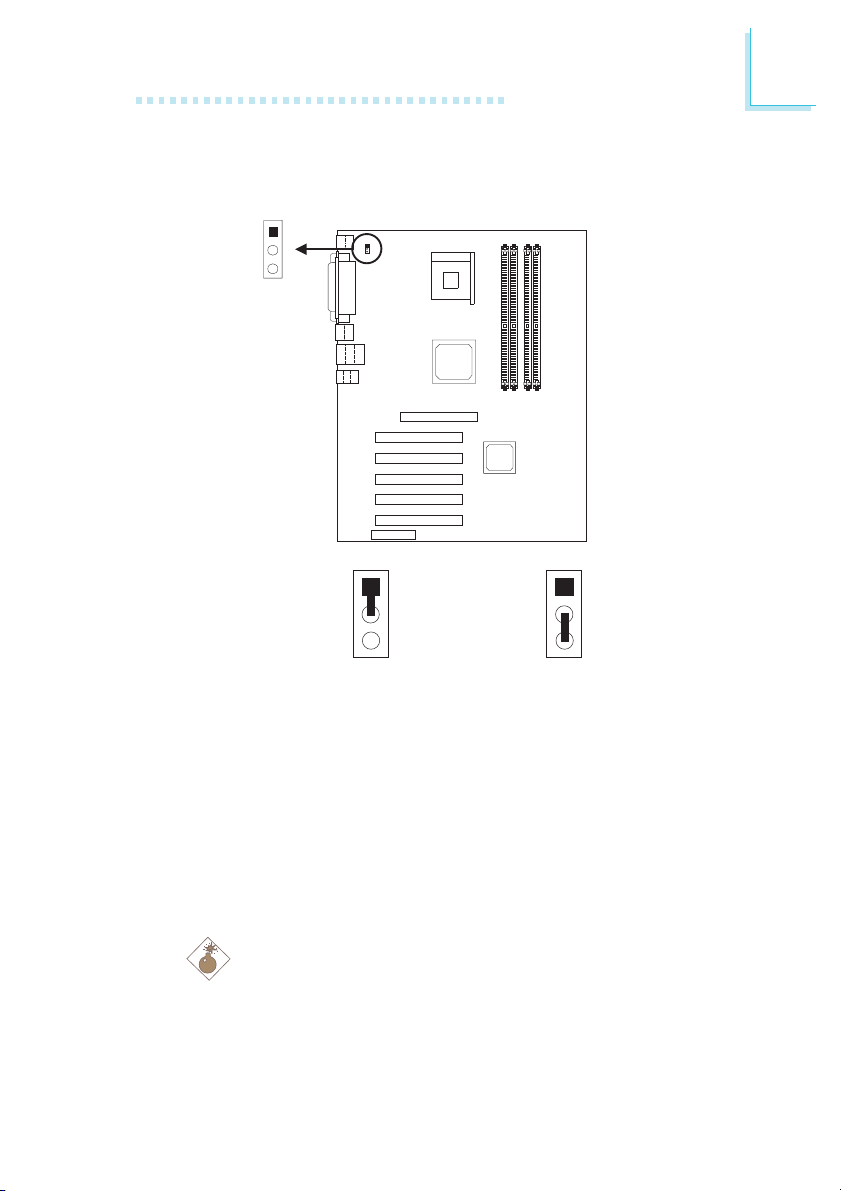
2.4 Jumper Settings for Wake-On-Keyboard/
Wake-On-Mouse
1
2
3
Wake-On-KB/
Mouse (JP1)
2
1
2
3
1-2 On: Disabled
2-3 On: Enabled
1
2
3
(default)
Wake-On-Keyboard/Wake-On-Mouse - Jumper JP1
The Wake-On-Keyboard/Wake-On-Mouse function allows you to use
the keyboard or PS/2 mouse to power-on the system. By default,
JP1 is disabled. To use this function, set JP1 to 2-3 On. “Keyboard/
Mouse Power On” (“Onboard Super IO Device” field) in the
Integrated Peripherals submenu of the BIOS must be set accordingly.
Refer to chapter 3 for details.
Warning:
1. If JP1 was enabled with a password set in the “KB Power
On Password” field, and now you wish to disable the
keyboard password function, make sure to set the
“Keyboard/Mouse Power On” field to Disabled prior to
setting JP1 to disabled. You will not be able to boot up the
system if you fail to do so.
23
Page 24

2
Hardware Installation
2. The power button will not function once a keyboard
password has been set in the “KB Power On Password”
(“Onboard Super IO Device” field) of the Integrated
Peripherals submenu. You must type the correct password
to power-on the system.
3. The 5VSB power source of your power supply must
support ≥720mA.
24
Page 25
Hardware Installation
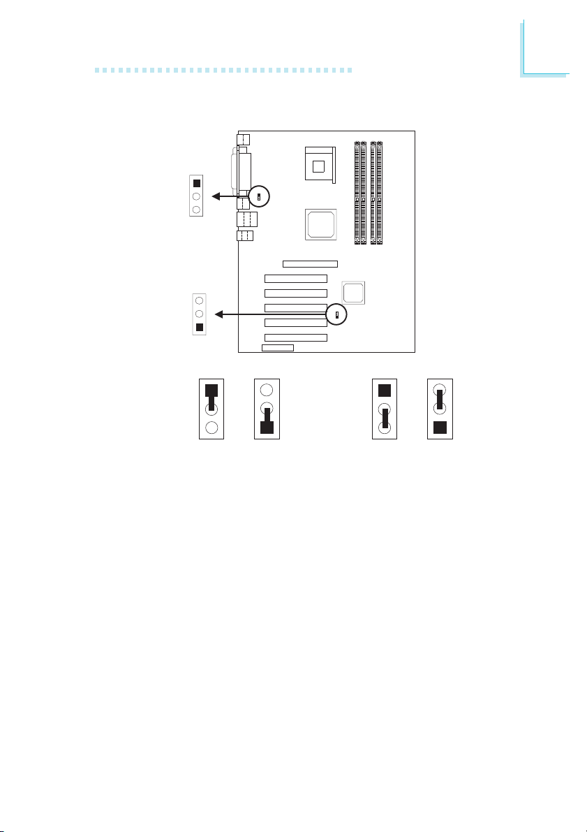
2.5 Jumper Settings for Wake-On-USB Keyboard
1
2
3
Wake-On-USB
1/2/3/4 (JP2)
3
2
1
Wake-On-USB
5/6 (JP7)
2
1
2
3
JP2 JP2
1-2 On: Disabled
JP7
3
2
1
1
2
3
3
2
1
JP7
2-3 On: Enabled
(default)
Wake-On-USB Keyboard for USBs 1 to 4 - Jumper JP2 and
Wake-On-USB Keyboard for USBs 5 and 6 - Jumper JP7
The Wake-On-USB Keyboard function allows you to use a USB
keyboard to wake up a system from the S3 (STR - Suspend To
RAM) state.
Regardless of the USB port enabled, make sure “USB KB Wake-Up
From S3” in the Power Management Setup submenu of the BIOS is
set to Enabled. “USB Controller” in the Integrated Peripherals
submenu of the BIOS must also be set appropriately.
25
Page 26

2
Hardware Installation
Important:
• If you are using the Wake-On-USB Keyboard function for 2
USB ports, the 5VSB power source of your power supply
must support ≥1.5A.
• If you are using the Wake-On-USB Keyboard function for 3
or more USB ports, the 5VSB power source of your power
supply must support ≥2A.
26
Page 27
Hardware Installation
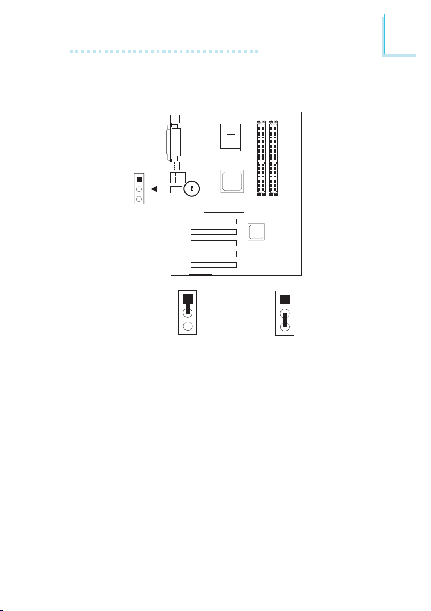
2.6 Jumper Settings for Selecting the CPU’s Front
Side Bus
1
2
3
CPU FSB select
(JP3)
2
1
2
3
1-2 On: 100MHz
2-3 On: Auto
1
2
3
(default)
CPU Front Side Bus Select - Jumper JP3
This jumper is used to select the front side bus of the CPU installed
on the system board.
27
Page 28
2
Hardware Installation
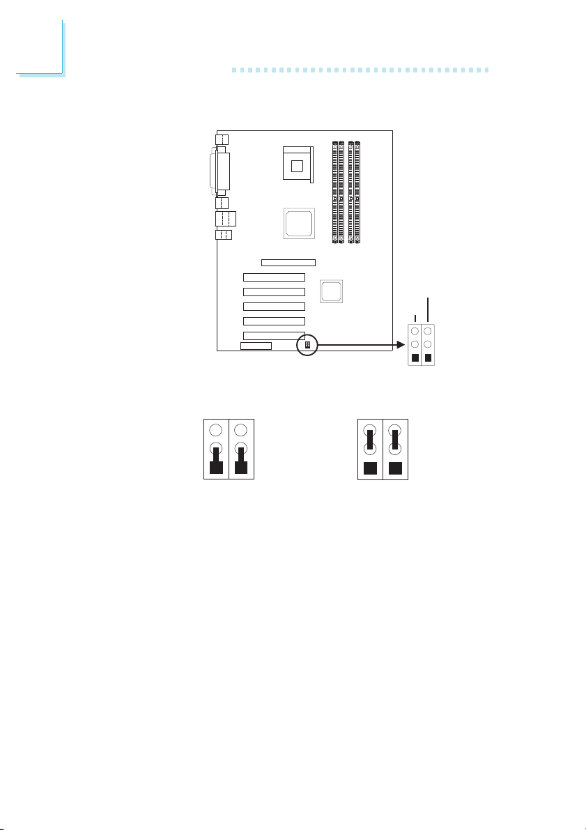
2.7 Jumper Settings for USB 6
J28
J27
3
2
1
USB 6 select
(J27/J28)
28
J27 J28
3
2
1
1-2 On: USB 6 on J19/J21
2-3 On: USB 6 on CNR
J27 J28
3
2
1
(default)
USB 6 Select - Jumpers J27 and J28
These jumpers are used to select USB 6’s location. Set pins 1 and 2
to On if you want USB 6 on J19/J21. Set pins 2 and 3 to On if you
want USB 6 on CNR.
Page 29
Hardware Installation
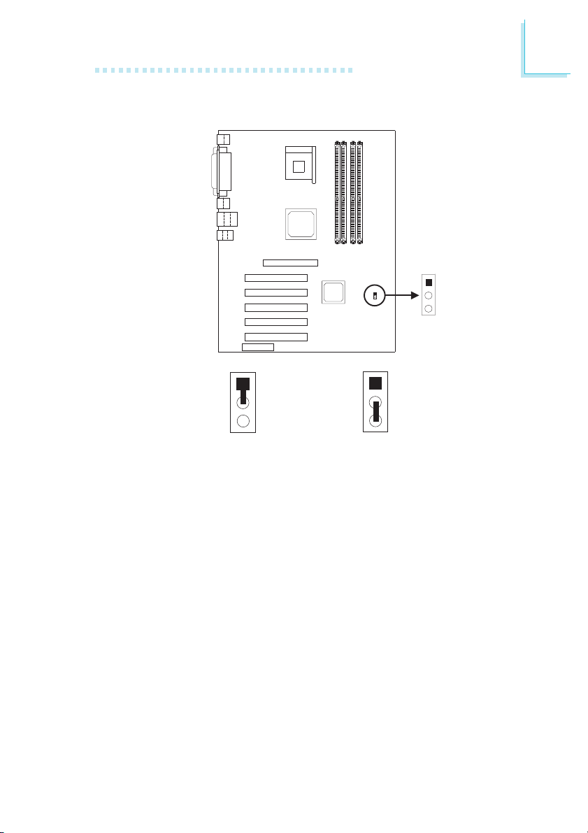
2.8 Jumper Settings for Serial ATA
2
1
2
3
SATA settings
(JP4)
1
2
3
1-2 On: Enabled
2-3 On: Disabled
1
2
3
(default)
Serial ATA Settings - Jumper JP4
This jumper is used to enable or disable the onboard Serial ATA
function.
Disabled - This is the default setting.
Enabled - If the onboard Serial ATA is enabled, you must set JP10
appropriately. Please refer to the next page for more
information.
29
Page 30
2
Hardware Installation
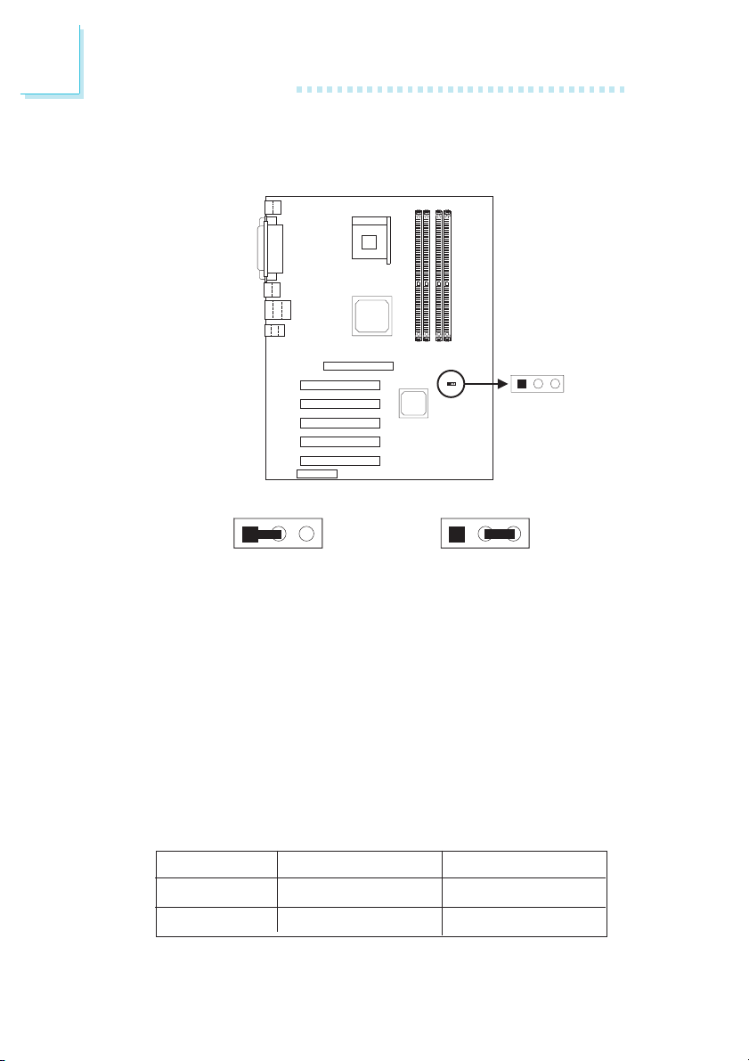
2.9 Jumper Settings for Serial ATA’s Master/Slave
Select
3
12
SATA Master/
Slave select
(JP10)
30
23
1
1-2 On: Master/Slave
(default)
Serial ATA’s Master/Slave Settings - Jumper JP10
This jumper must be configured only if the onboard Serial ATA is
enabled (JP4 pins 1 and 2 set to On).
Master/Slave - If you set JP10 to Master/Slave, the Serial ATA device
must be set to Master mode and the device connected to IDE 1
must be set to Slave mode.
Master - If you set JP10 to Master, the Serial ATA device must be
set to Master mode. Do not connect any device to IDE 1.
Serial ATA Device
Master/Slave
Master
Master
Master
23
1
2-3 On: Master
IDE 1 Device
Slave
No device
Page 31
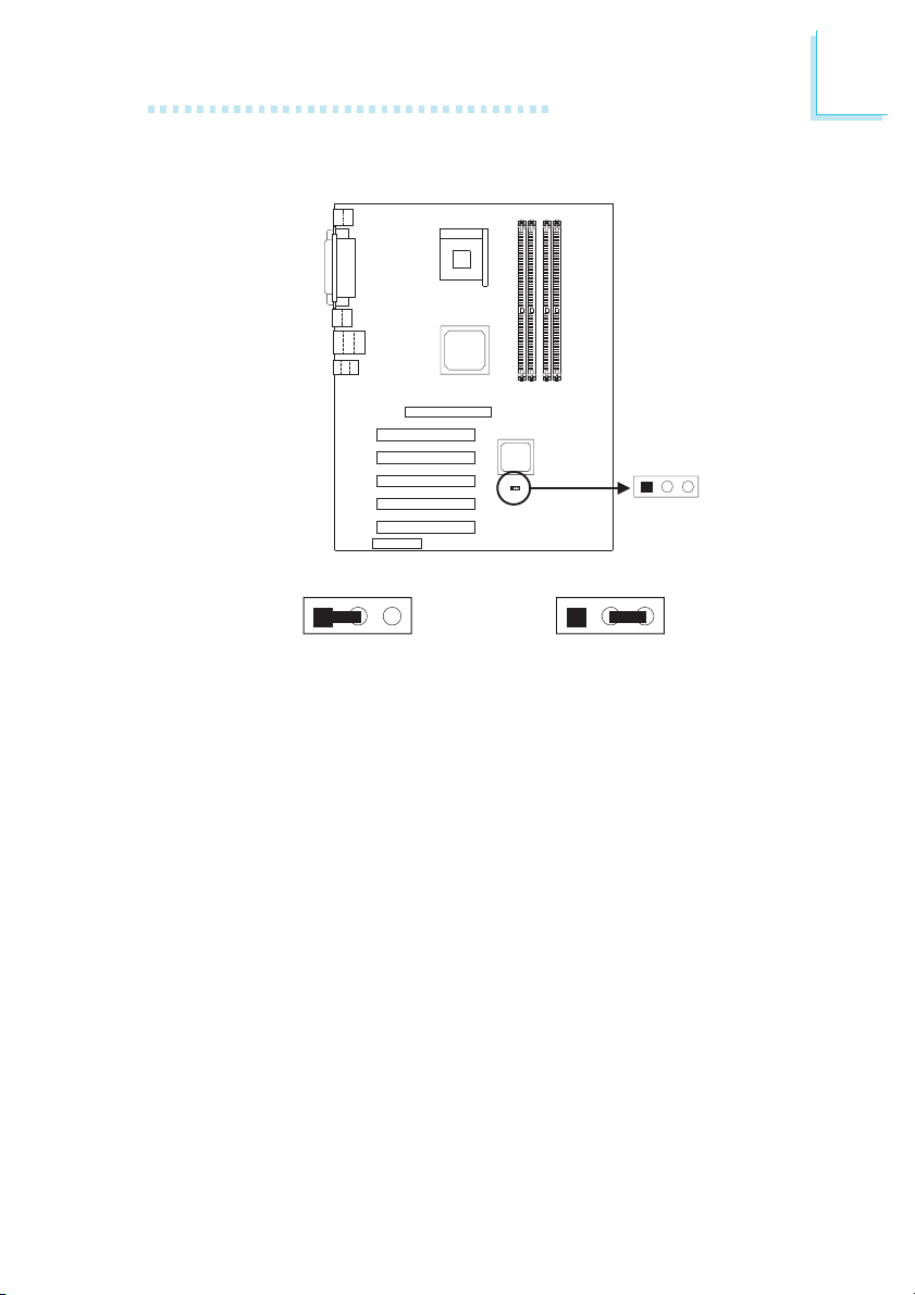
2.10 Jumper Settings for RAID
Hardware Installation
3
12
RAID settings
(JP6)
2
23
1
1-2 On: Enabled
RAID Settings - Jumper JP6
This jumper is used to enable or disable the onboard RAID function.
The “RAID or SCSI Card Boot” field in the Advanced BIOS Features
submenu of the BIOS must also be set appropriately.
2-3 On: Disabled
23
1
(default)
31
Page 32
2
Hardware Installation
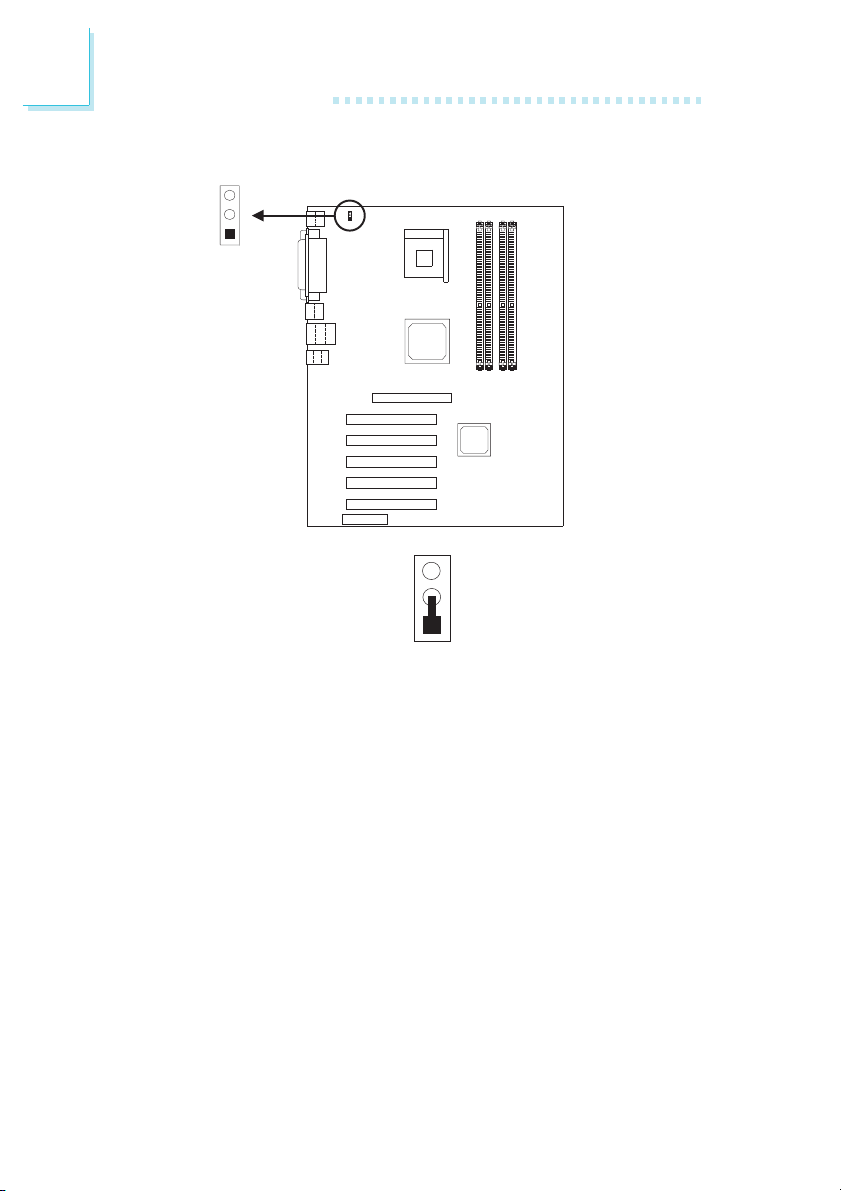
2.11 Factory Use Jumper
3
2
1
Factory use only
(J1)
3
2
1
1-2 On: Default
32
Factory Use Only - Jumper J1
This jumper is for factory use only. Please leave it in its default
setting. Reconfiguring the jumper may cause problems.
Page 33
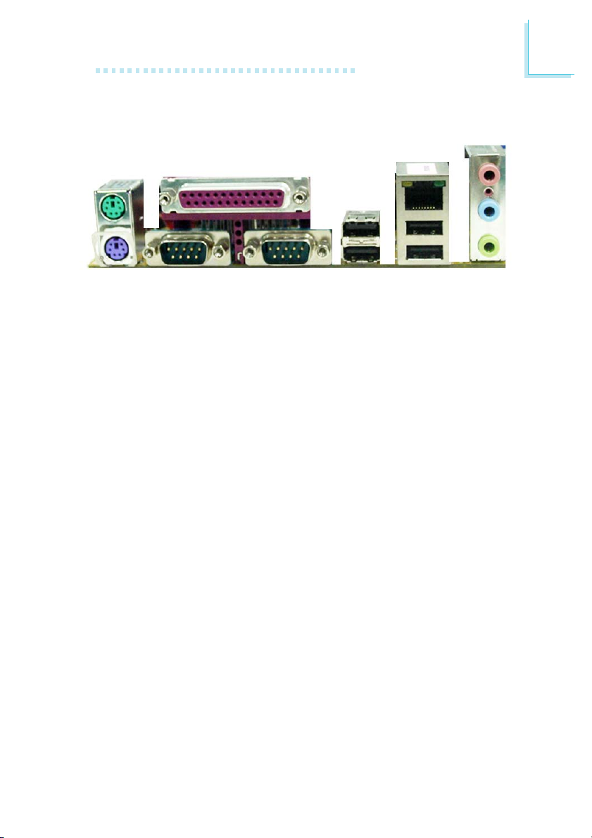
2.12 Rear Panel I/O Ports
PS/2
Mouse
Parallel
Hardware Installation
RJ45
LAN
2
Mic-in
PS/2
K/B
COM 1
COM 2
USB 2
USB 1
Line-in
Line-out
USB 4/3
33
Page 34
2
Hardware Installation
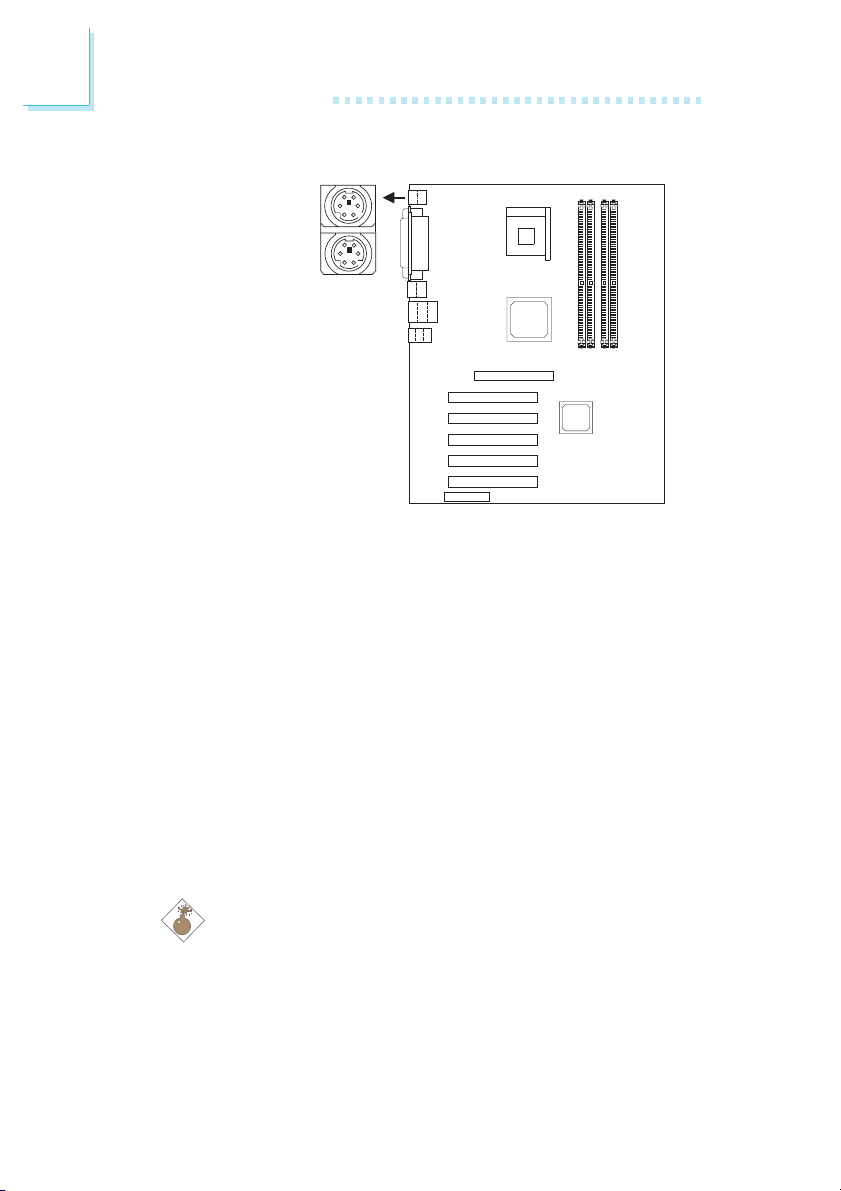
2.12.1 PS/2 Mouse and PS/2 Keyboard Ports
PS/2 Mouse
PS/2 Keyboard
The onboard PS/2 mouse (Green) and PS/2 keyboard (Purple)
ports are at location J4 of the system board. The PS/2 mouse port
uses IRQ12. If a mouse is not connected to this port, the system
will reserve IRQ12 for other expansion cards.
The Wake-On-Keyboard/Mouse function allows you to use the
keyboard or PS/2 mouse to power-on the system.
To use this function:
J4
• JP1 pins 2 and 3 must be set to On.
34
• “Keyboard/Mouse Power On” (“Onboard Super IO Device” field)
in the Integrated Peripherals submenu of the BIOS must be set
accordingly. Refer to chapter 3 for more information.
Warning:
Make sure to turn off your computer prior to connecting or
disconnecting a mouse or keyboard. Failure to do so may
damage the system board.
Page 35
Hardware Installation
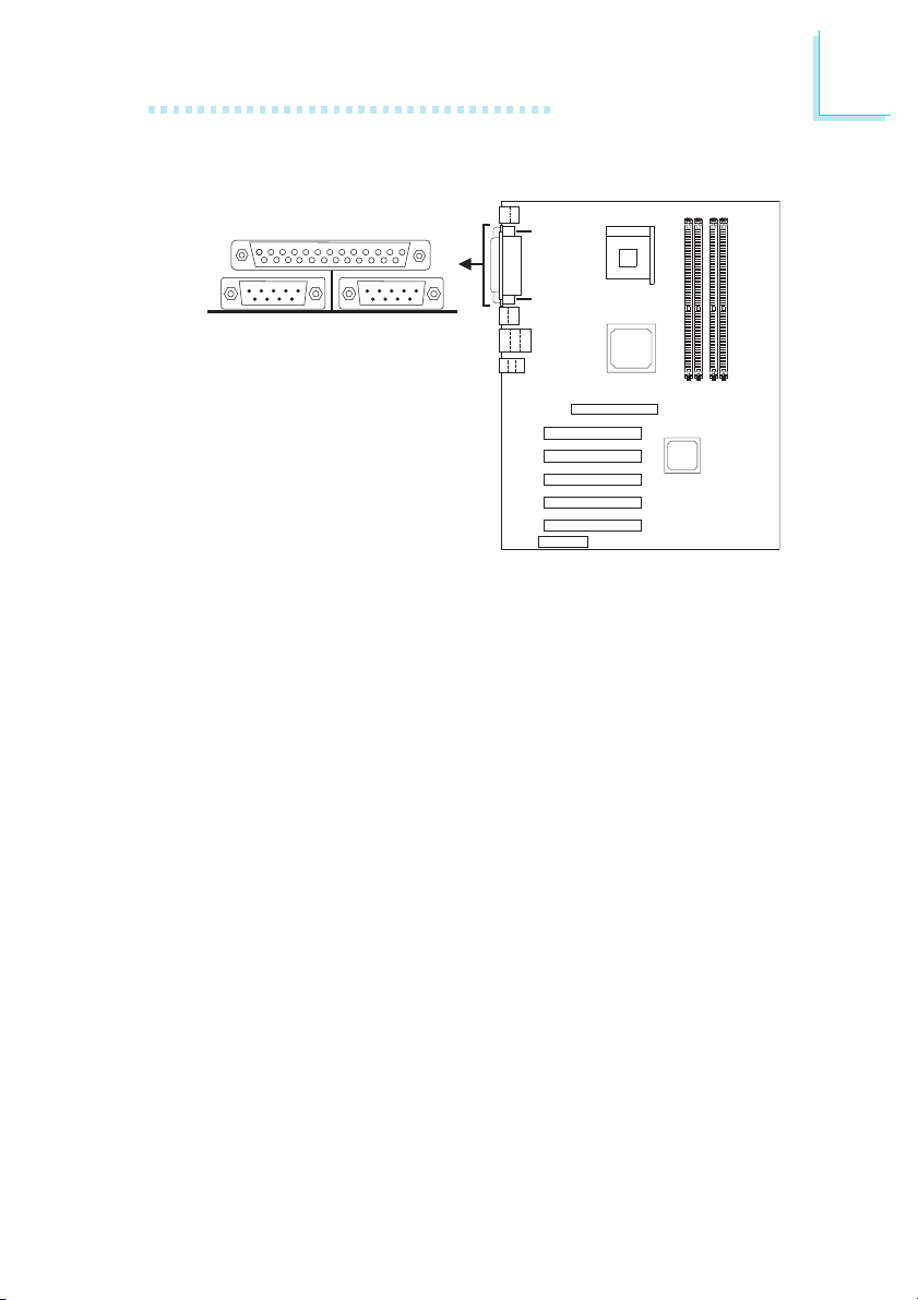
2.12.2 Serial Ports
CN1
CN3
COM 1
Serial Port
The onboard serial ports, both in Teal/Turquoise color, are at
locations CN1 (COM 1) and CN3 (COM 2) of the system board.
These ports are RS-232C asynchronous communication ports with
16C550A-compatible UARTs that can be used with modems, serial
printers, remote display terminals, and other serial devices. You can
select the serial ports’ I/O address in the Integrated Peripherals
submenu (“Onboard Super IO Device” field) of the BIOS.
COM 2
Serial Port
2
35
Page 36
2
CN2
Hardware Installation
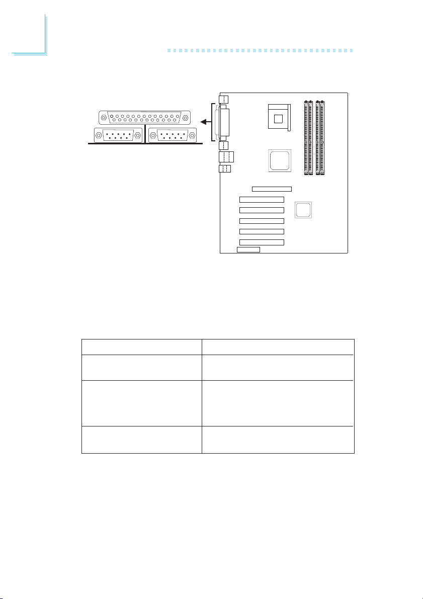
2.12.3 Parallel Port
Parallel Port
The standard parallel port (Burgundy) at location CN2 of the
system board is for interfacing your PC to a parallel printer. It supports SPP, ECP and EPP modes. You can select the port’s mode in
the Integrated Peripherals submenu (“Onboard Super IO Device”
field) of the BIOS.
36
Setting
SPP
(Standard Parallel Port)
ECP
(Extended Capabilities Port)
EPP
(Enhanced Parallel Port)
Function
Allows normal speed operation but
in one direction only.
Allows parallel port to operate in
bidirectional mode and at a speed
faster than the SPP’s data transfer
rate.
Allows bidirectional parallel port operation at maximum speed.
Page 37
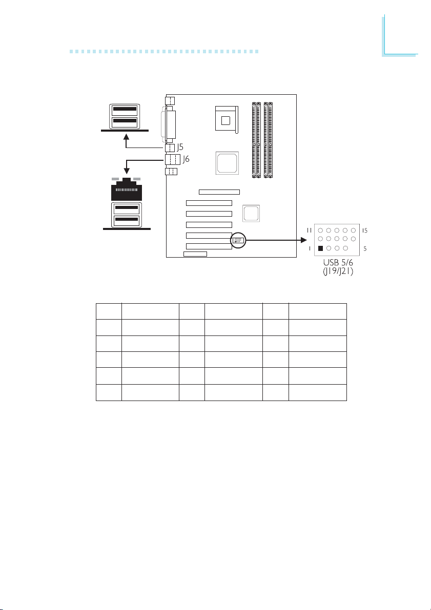
2.12.4 Universal Serial Bus Ports
USB 2
USB 1
USB 4
USB 3
Additional USB Ports (USB 5/6)
Hardware Installation
2
Pin
1
2
3
4
5
Function
VCC
UP5-
UP5+
Ground
Key
Pin
6
7
8
9
10
Function
VCC
UP6-
UP6+
Ground
N. C.
Pin
11
12
13
14
15
Function
Ground
Ground
UP5+
UP5-
VCC
37
Page 38

2
Hardware Installation
The system board supports 6 USB 2.0/1.1 ports. USB 1.1 supports
12Mb/second bandwidth while USB 2.0 supports 480Mb/second
bandwidth providing a marked improvement in device transfer
speeds between your computer and a wide range of simultaneously
accessible external Plug and Play peripherals.
Four onboard USB 2.0/1.1 ports (Black) are at locations J5 and J6
of the system board.
Depending on the type of USB port cable that you are using, the
J19/J21 connector on the system board allows you to connect 2
additional USB 2.0/1.1 ports. These USB ports, which are mounted
on a card-edge bracket, will be provided as an option. If you wish to
use the optional USB ports, install the card-edge bracket to the
system chassis then insert the connector that is attached to the USB
port cables to J19/J21.
Insert the USB port cable connector to pins 1-10 if:
• One of the holes on the cable connector is plugged, meaning the
cable connector has a keying mechanism.
Insert the USB port cable connector to pins 6-15 if:
38
• None of the holes on the cable connector is plugged, meaning
the cable connector has no keying mechanism.
“USB Controller” in the Integrated Peripherals submenu of the BIOS
is used to enable or disable the USB ports. Make sure this field is
set appropriately.
The system board supports the Wake-On-USB Keyboard function. To
use this function:
• JP2 and/or JP7 pins 2 and 3 must be set to On.
• “USB KB Wake-Up From S3” in the Power Management Setup
submenu of the BIOS must be set accordingly. Refer to chapter
3 for more information.
Page 39
Hardware Installation
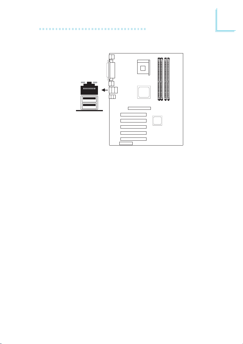
J6
2.12.5 RJ45 Fast-Ethernet Port
RJ45 LAN
The system board is equipped with an onboard RJ45 fast-ethernet
LAN port at location J6. It allows the system board to connect to a
local area network by means of a network hub. The Realtek
RTL8100 chip that controls this port can be enabled or disabled in
the Integrated Peripherals submenu (“Intel OnChip PCI Device” field)
of the BIOS. Refer to the Integrated Peripherals section in chapter 3
for more information.
2
39
Page 40
2
Hardware Installation
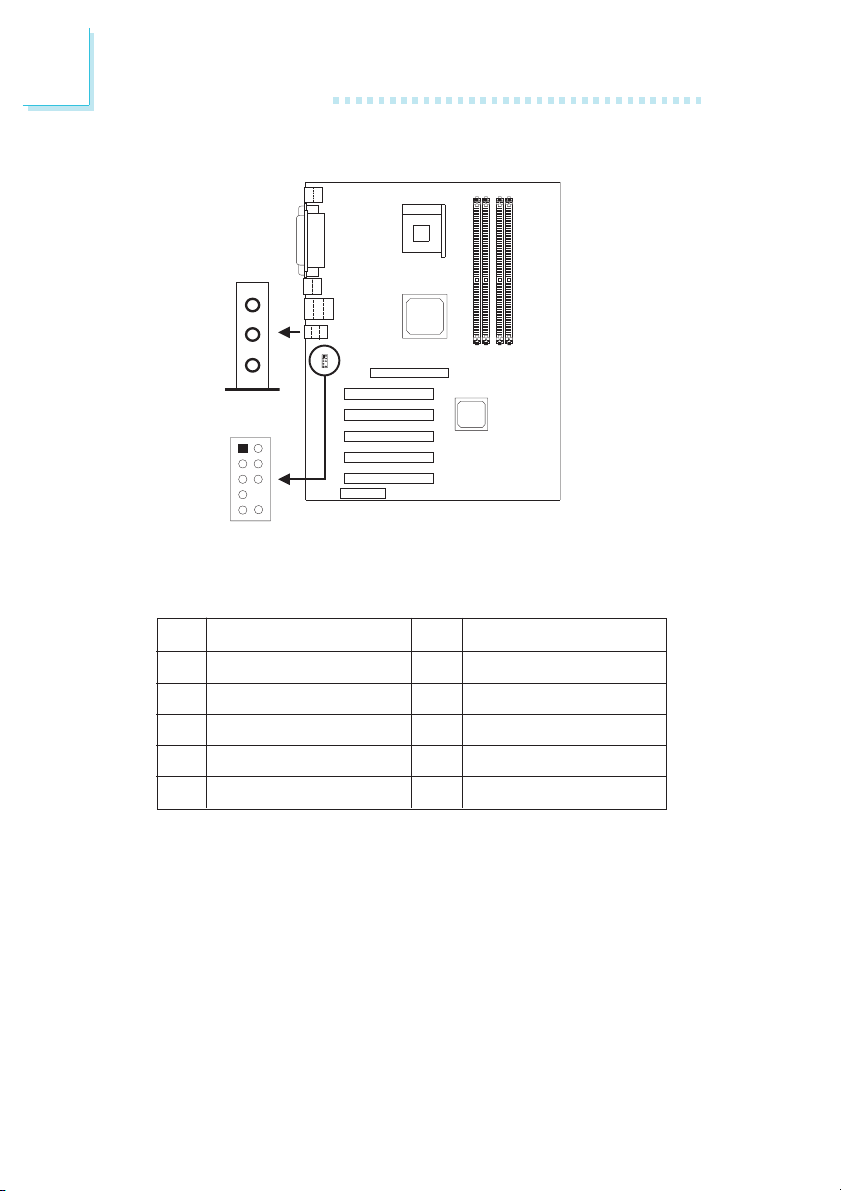
2.12.6 Audio Jacks
Mic-in
Line-in
Line-out
2
1
10
9
Front audio
(J11)
Front Audio (J11)
40
Pin
1
3
5
7
9
Function
Mic+
Vbias
AuD_R_Out
N. C.
AuD_L_Out
Function
Pin
Ground
2
AuD_Vcc (Avcc)
4
N. C .
6
Key
8
N. C .
10
Page 41

Hardware Installation
Onboard Audio Jacks
The system board is equipped with 3 audio jacks. A jack is a onehole connecting interface for inserting a plug.
Line-out Jack (Lime)
This jack is used to connect external speakers for audio output from
the system board.
Line-in Jack (Light Blue)
This jack can be connected to the line-out jack of any external audio
devices such as Hi-fi set, CD player, AM/FM radio tuner, synthesizer,
etc. Connect a stereo cable from the line-out jack of your external
device to this line-in jack.
Mic-in Jack (Pink)
Connect a microphone to the mic-in jack.
Front Audio (J11)
J11 provides you the option of connecting another line-out and micin jacks.
2
41
Page 42
2
Hardware Installation
2.13 I/O Connectors
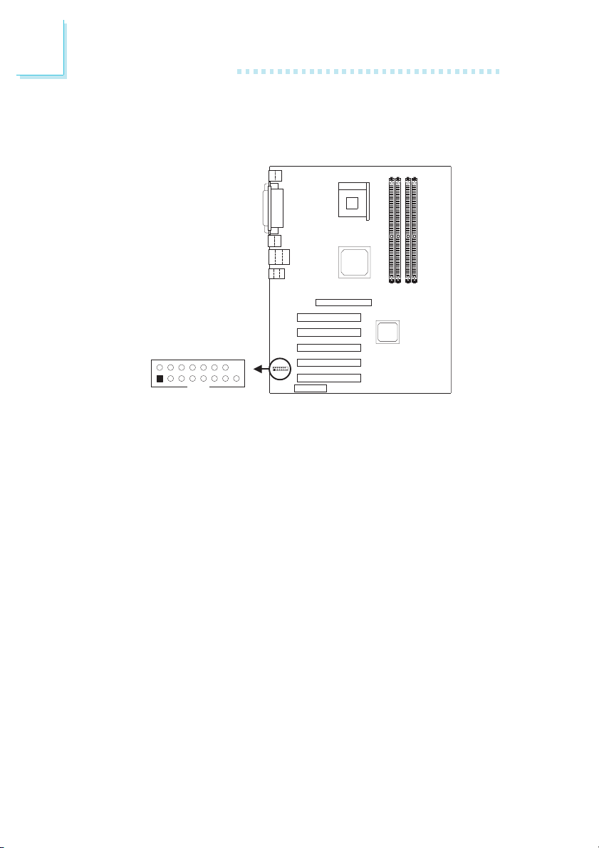
2.13.1 Game/MIDI Port
2
1
Game/MIDI
(J20)
The system board is equipped with a 15-pin connector at location
J20 for connecting an external game/MIDI port. One card-edge
bracket, mounted with a game/MIDI port cable, is provided with the
system board. Install the card-edge bracket to the system chassis
then connect the game/MIDI port cable to connector J20. Make sure
the colored stripe on the ribbon cable is aligned with pin 1 of
connector J20.
The Game/MIDI port is identical to that of a standard PC game
adapter or game I/O port. This port works well with any application
that is compatible with the standard PC joystick. You can configure
the game port in the Integrated Peripherals submenu (“Onboard
Super IO Device” field) of the BIOS.
15
42
Page 43
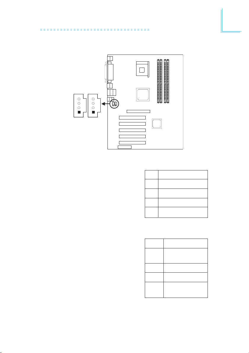
2.13.2 Internal Audio Connectors
4
3
2
1
TAD
CD-in
(J8)
(J9)
CD-in
Hardware Installation
2
This connector is used to receive
audio from a CD-ROM drive, TV
tuner or MPEG card.
TAD
TAD is a connector for telephony
audio devices such as voice modem
cards. By installing a PCI voice
modem card that is also equipped
with a TAD connector, connect one
end of the cable (that came with
the card) to the card’s TAD
connector and the other end to the
TAD connector on the system
board. The voice modem will
interface with the onboard audio
allowing voice to come from the
external speaker.
Pin
1
2
3
4
Pin
1
2
3
4
Function
Left audio channel
Ground
Ground
Right audio channel
Function
Modem-out
(from modem)
Ground
Ground
Modem-in
(to modem)
43
Page 44
2
Hardware Installation
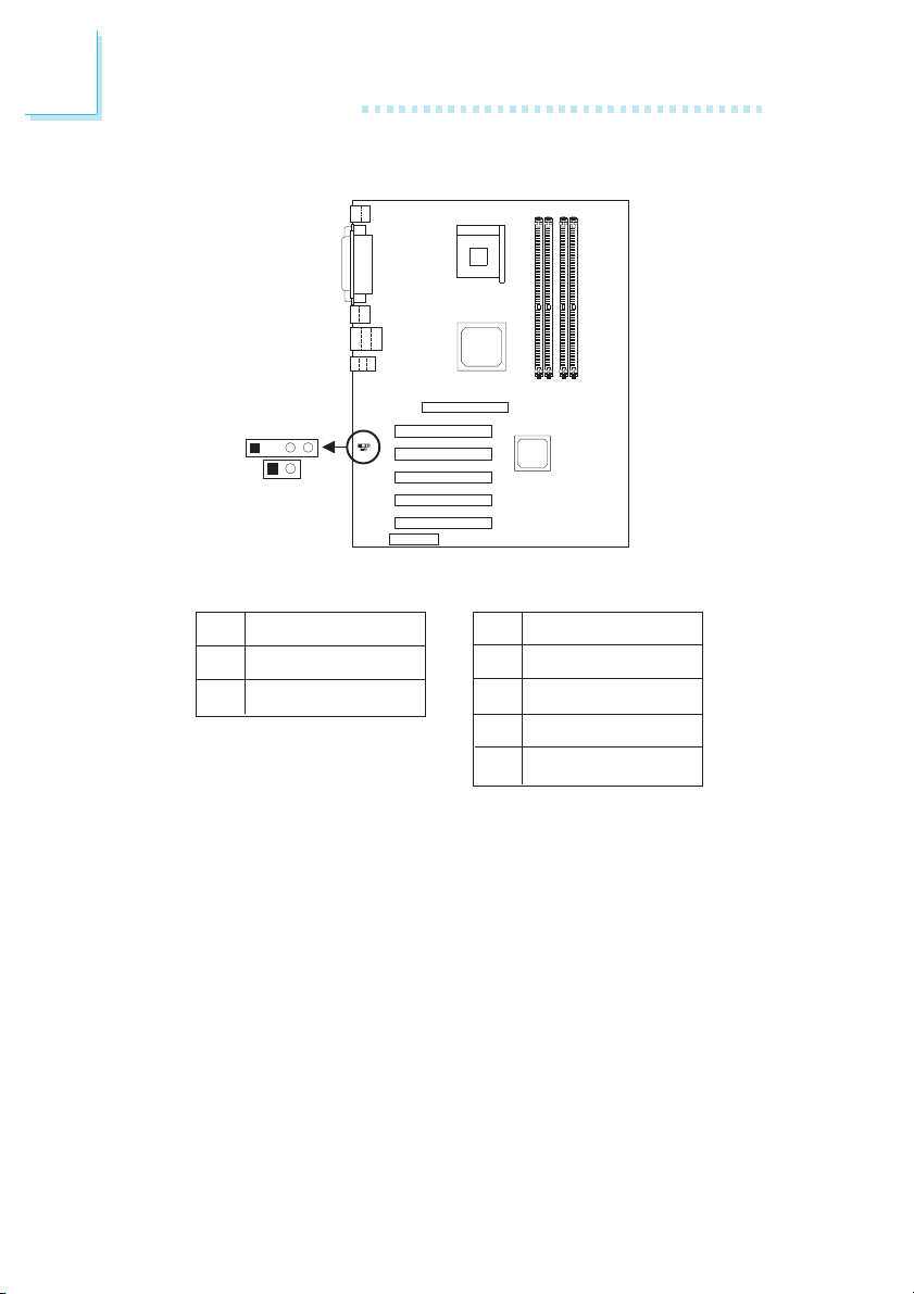
2.13.3 S/PDIF-in and S/PDIF-out Connectors
S/PDIF-out
(J15)
1234
21
S/PDIF-in
(J16)
Pin
1
2
3
4
S/PDIF-out
Function
AVDD5
N. C .
SPDIF
Ground
S/PDIF-in
Pin
1
2
The system board is equipped with a digital audio interface - S/PDIF
(Sony/Philips Digital Interface). S/PDIF is a standard audio file transfer
format that transfers digital audio signals to a device without having
to be converted first to an analog format. This prevents the quality
of the audio signal from degrading whenever it is converted to
analog.
One card-edge bracket, mounted with a S/PDIF-in connector and
S/PDIF-out connector, will be provided as an option. Install the cardedge bracket to the system chassis then connect the appropriate
audio cable connectors to J15 and J16. Make sure pin 1 of the
cable connectors is aligned with pin 1 of J15 and J16. Now connect
external speakers or a device that suppor ts digital output to the
S/PDIF-in and S/PDIF-out connectors.
Function
SPDIF-in
Ground
44
Page 45
Hardware Installation
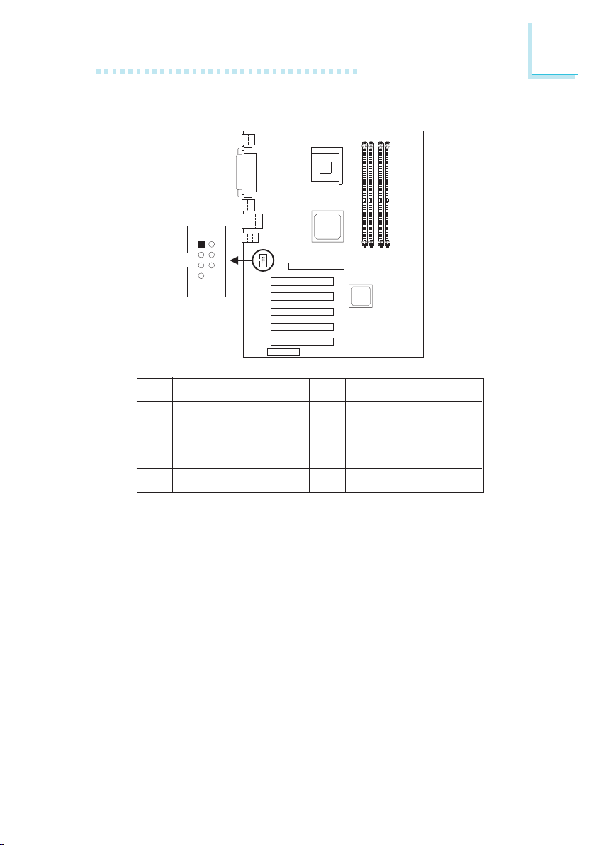
2.13.4 4-Channel Audio Output Connector
2
(J10)
Function
SL
Ground
SR
Ground
2
2
4
6
8
Function
Center out
Ground
LFE Out
Key
Pin
1
7
4CH audio
Pin
1
3
5
7
The 4-channel audio connector (J10) supports 4 audio output
signals: center channel, subwoofer, rear right channel and rear left
channel.
45
Page 46
2
Hardware Installation
2.13.5 Smart I/O Connectors
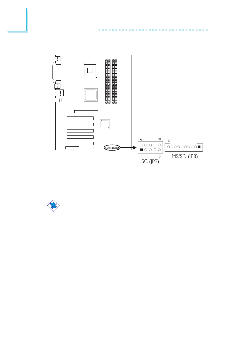
The system board is equipped with a Smart Card (SC) interface
(security interface) and a MS/SD interface (compact storage
interface). Use the optional Smart I/O drive to insert these cards.
46
Note:
The MS/SD interface allows you to connect either a Memory
Stick (MS) or Secure Digital Memory Card (SD). You cannot use
both at the same time.
The Smart Card is a small electronic device about the size of a
credit card that provides security to files or computer. The extent
and type of security will depend on the settings built into the card.
Memory Stick is an IC memory media that has a large storage
capacity. It can store any format of digital data as well as transfer
digital data and shares them among electronic devices that are
compatible with Memory Stick.
Secure Digital Memory Card is a storage device about the size of a
postage stamp that provides fast downloading of all types of digital
files to your computer as well as easy transfer of files from your
computer to the SD Memory Card.
Page 47

Hardware Installation
You can select the SC and MS/SD’s address/IRQ in the Integrated
Peripherals submenu (“Onboard Super IO Device” field) of the BIOS.
Smart Card Interface
2
Pin
1
2
3
4
5
Pin
1
2
3
4
5
Function
VCC
SCAPWC-
SCAC4
SCAIO
SCACLK
Memory Stick / Secure Digital Memory Card Interface
Function
Ground
MSA1
VCC3
MSA2
MSA3
Pin
10
Pin
10
6
7
8
9
6
7
8
9
Function
Ground
SCARST-
SCALED
SCAC8
SCAPSNT
Function
MSA4
MSA5
MSACLK
MSAPWC-
MSALED
47
Page 48
2
Hardware Installation
2.13.6 Floppy Disk Drive Connector
34
2
FDD
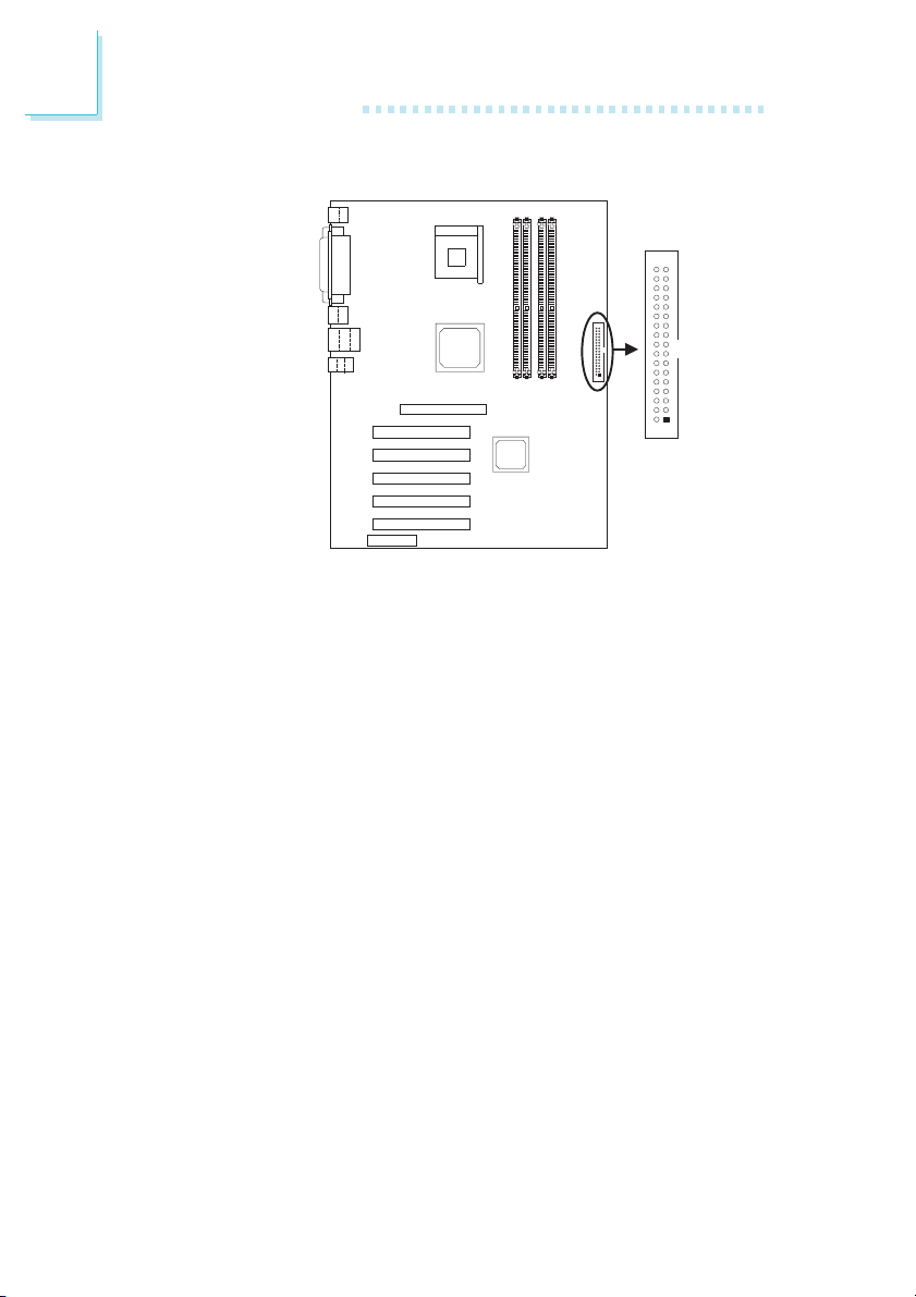
The system board is equipped with a shrouded floppy disk drive
connector that supports two standard floppy disk drives. To prevent
improper floppy cable installation, the shrouded floppy disk header
has a keying mechanism. The 34-pin connector on the floppy cable
can be placed into the header only if pin 1 of the connector is
aligned with pin 1 of the header. You may enable or disable this
function in the Integrated Peripherals submenu (“Onboard Super IO
Device” field) of the BIOS.
33
1
(J7)
48
Connecting the Floppy Disk Drive Cable
1. Install the 34-pin header connector of the floppy disk drive cable
into the shrouded floppy disk header (J7) on the system board.
The colored edge of the ribbon should be aligned with pin 1 of
J7.
2. Install the other 34-pin header connector(s) into the disk drive(s).
Align the colored edge of the daisy chained ribbon cable with pin
1 of the drive edge connector(s). The end-most connector should
be attached to the drive you want to designate as Drive A.
Page 49
Hardware Installation
2.13.7 Serial ATA IDE Connector
SATA
(J14)
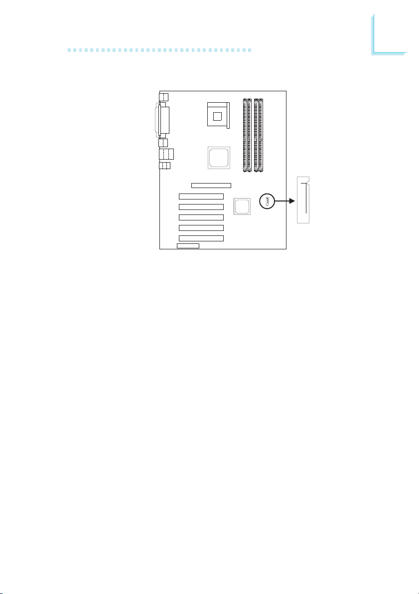
Serial ATA is a storage interface that is compliant with SATA 1.0
specification. With speed of up to 1.5Gbps, it improves hard drive
performance even in data intensive environments such as audio/
video, consumer electronics and entr y-level servers.
One Serial ATA cable will be provided as an option. Connect one
end of the cable to J14 and the other end to your serial ATA
device. Jumper JP4 pins 1 and 2 must be set to On (Enabled). JP10
must also be set accordingly.
2
49
Page 50
2
Hardware Installation
2.13.8 IDE Disk Drive Connector
40
2
39
1
IDE 2
(J12)
40
2
39
1
IDE 1
(J13)
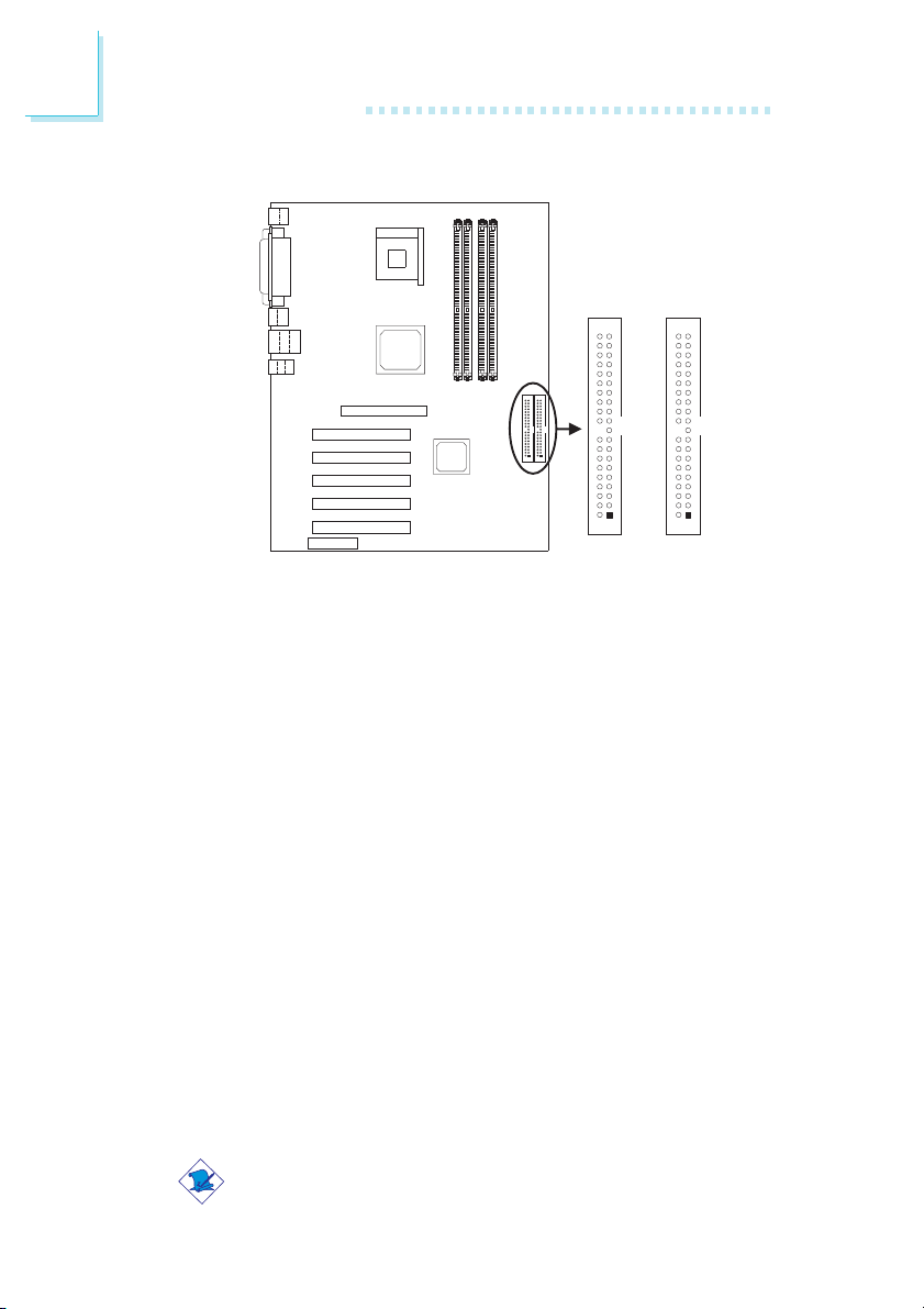
The system board is equipped with two shrouded PCI IDE headers
that will interface four Enhanced IDE (Integrated Drive Electronics)
disk drives. To prevent improper IDE cable installation, each shrouded
PCI IDE header has a keying mechanism. The 40-pin connector on
the IDE cable can be placed into the header only if pin 1 of the
connector is aligned with pin 1 of the header. You may enable or
disable the onboard primary or secondary IDE controller in the
Integrated Peripherals submenu (“INTEL OnChip IDE Device” field)
of the BIOS.
Connecting the IDE Disk Drive Cable
1. If you are connecting two IDE drives, install the 40-pin connector
of the IDE cable into the primary shrouded IDE header (J13). If
you are adding a third or fourth IDE device, install the 40-pin
connector of the other IDE cable into the secondary shrouded
IDE header (J12).
50
2. Install the other 40-pin header connector(s) into the device with
the colored edge of the ribbon cable aligned with pin 1 of the
drive edge connector(s).
Note:
Refer to your disk drive user’s manual for information about
selecting proper drive switch settings.
Page 51

Hardware Installation
Adding a Second IDE Disk Drive
When using two IDE drives, one must be set as the master and the
other as the slave. Follow the instructions provided by the drive
manufacturer for setting the jumpers and/or switches on the drives.
The system board supports Enhanced IDE or ATA-2, ATA/33,
ATA/66 or ATA/100 hard drives. We recommend that you use hard
drives from the same manufacturer. In a few cases, drives from two
different manufacturers will not function properly when used together.
The problem lies in the hard drives, not the system board.
Important:
If you encountered problems while using an ATAPI CD-ROM
drive that is set in Master mode, please set the CD-ROM drive
to Slave mode. Some ATAPI CD-ROMs may not be recognized
and cannot be used if incorrectly set in Master mode.
2
51
Page 52
2
Hardware Installation
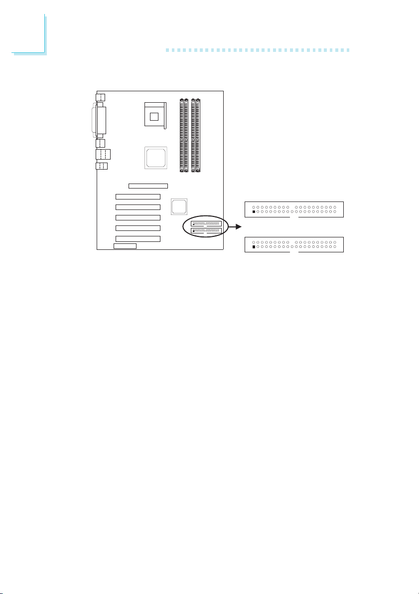
2.13.9 RAID IDE Disk Drive Connectors
2
RAID IDE 1 (J17)
40
1
2
1
RAID IDE 2 (J18)
39
40
39
The system board is equipped with two shrouded RAID IDE
headers that will interface four Enhanced IDE (Integrated Drive
Electronics) disk drives. To prevent improper IDE cable installation, the
shrouded RAID IDE header has a keying mechanism. The 40-pin
connector on the IDE cable can be placed into the header only if pin
1 of the connector is aligned with pin 1 of the header.
Hard drives must be Ultra ATA/100, Ultra ATA/66, Ultra ATA/33,
EIDE and/or Fast ATA-2 compatible. For optimal performance, install
identical drives of the same model and capacity. The drives’ matched
performance allows the RAID array to function better as a single
drive.
Drives in an array must be identical. If striping for performance, use
two new drives. If mirroring for protection, you can use two new
drives or use an existing drive and a new drive (the new drive must
be the same size or larger than the existing drive). Only two drives
can be configured as RAID. Since both of these drives must be in
Master mode, striping or mirroring must be done between 2 RAID
IDE channels; not between 2 drives that are chained on the same
channel.
52
Page 53

Hardware Installation
Jumper JP6 pins 1 and 2 must be set to On (Enabled).
The “RAID or SCSI Card Boot” field in the Advanced BIOS Features
submenu of the BIOS must be set appropriately.
Note:
• Only connect IDE hard drives to the RAID IDE connectors.
• Refer to the RAID user’s manual included in the CD for
information on configuring RAID.
RAID User’s Manual
(Click here to open the manual.)(Click here to open the manual.)
(Click here to open the manual.)
(Click here to open the manual.)(Click here to open the manual.)
2
53
Page 54
2
Hardware Installation
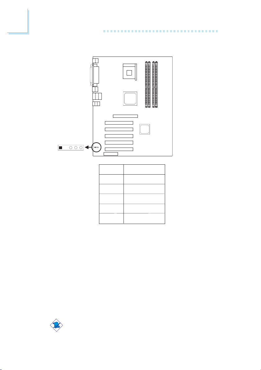
2.13.10 IrDA Connector
54
1234
The system board is equipped with an IrDA connector for wireless
connectivity between your computer and peripheral devices. The
IRDA (Infrared Data Association) specification supports data
transfers of 115K baud at a distance of 1 meter.
Connect your IrDA cable to connector J24 on the system board. Set
“UART2 Mode Select” (“Onboard Super IO Device” field) in the
Integrated Peripherals submenu of the BIOS to the type of IrDA
standard supported by your device. You must have the proper
drivers installed in your operating system to use this connector. Refer
to your operating system’s manual or documentation.
5
IrDA
(J24)
Pin
1
2
3
4
5
Note:
The sequence of the pin functions on some IrDA cable may be
reversed from the pin function defined on the system board.
Make sure to connect the cable to the IrDA connector
according to their pin functions.
Function
VCC
N. C .
IRRX
Ground
IRTX
Page 55
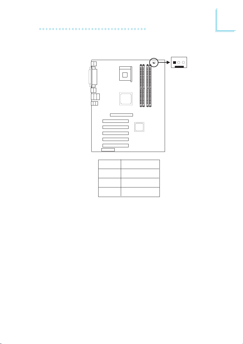
2.13.11 CPU Fan Connector
Hardware Installation
3
2
1
CPU fan
(J2)
2
Pin
1
2
3
The CPU must be kept cool by using a fan with heatsink. Connect
the CPU fan to the 3-pin fan connector at location J2 on the system
board. The system is capable of monitoring the speed of the CPU
fan.
Function
Ground
Power
Sense
55
Page 56
2
Hardware Installation
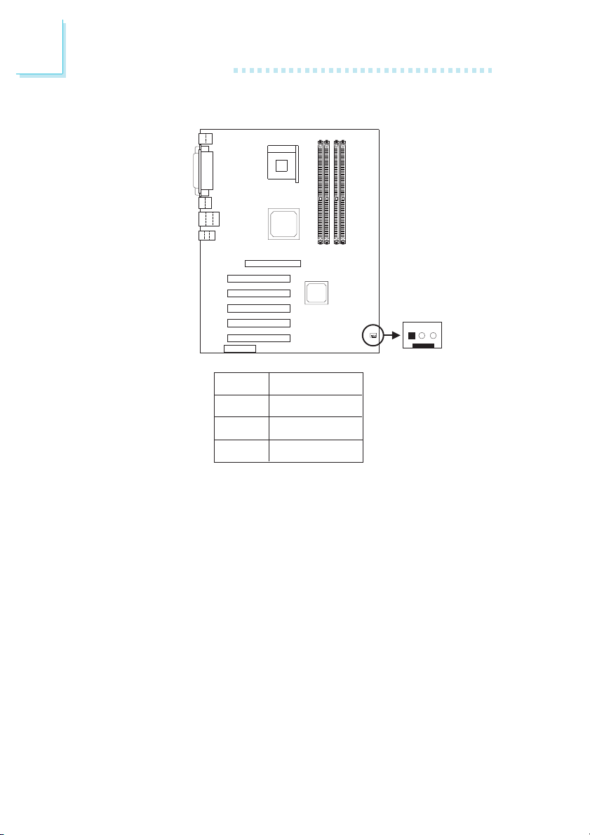
2.13.12 Chassis Fan Connector
Pin
1
2
3
Function
Ground
Power
Sense
3
2
1
Chassis fan
(J25)
56
If you are installing a chassis fan in the system unit, connect the fan’s
connector to location J25 on the system board. The fan will provide
adequate airflow throughout the chassis to prevent overheating the
CPU.
Page 57
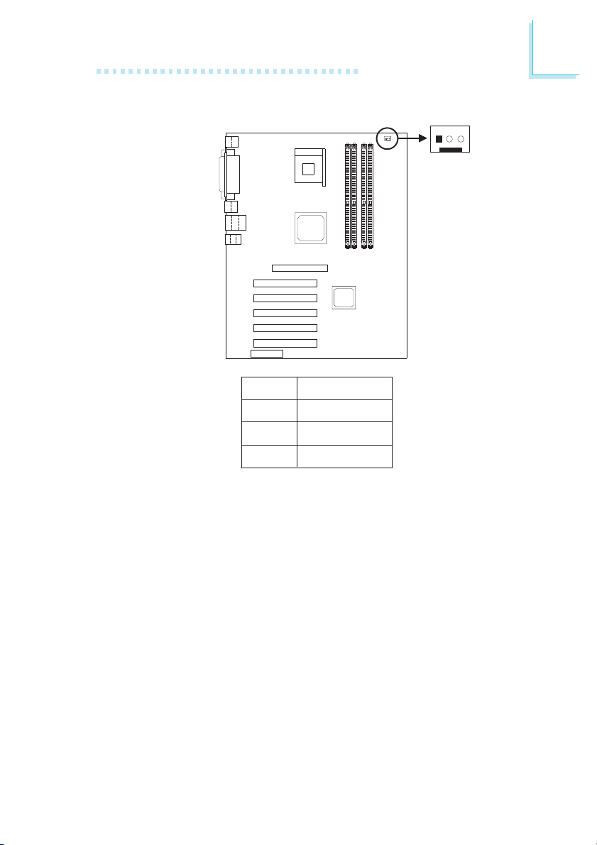
2.13.13 System Fan Connector
3
2
1
System fan
(J3)
Hardware Installation
2
Pin
1
2
3
If you are installing a system fan in the system unit, connect the fan’s
connector to location J3 on the system board. The system is capable
of monitoring and controlling the speed of the system fan. The
system fan will automatically turn off once the system enters the
Suspend mode.
Function
On/Off
Power
Sense
57
Page 58
2
Hardware Installation
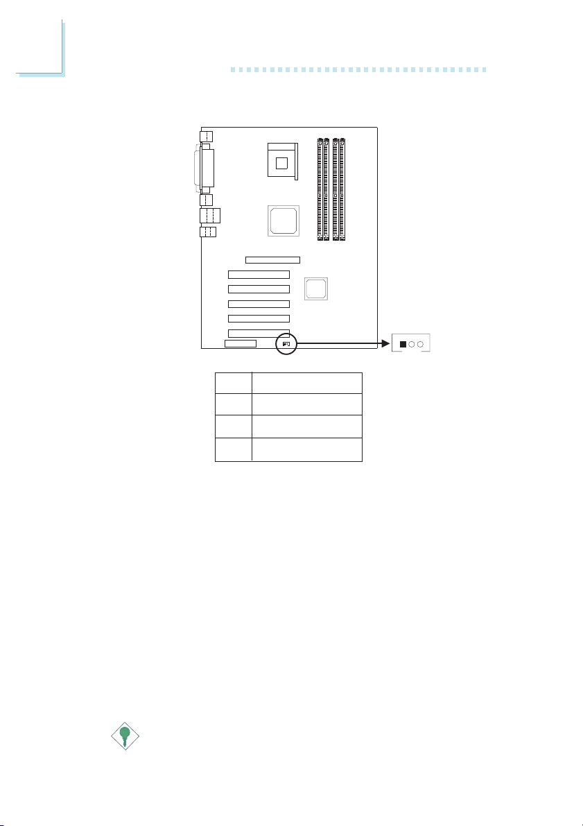
2.13.14 Wake-On-LAN Connector
Pin
1
2
3
Function
WOL
Ground
+5VSB
3
21
Wake-On-LAN
(J30)
58
The Wake-On-LAN function is applicable only when you are using a
LAN add-in card that has the same function. It will allow the
network to remotely power-on a Soft Power Down (Soft-Off) PC.
However, if your system is in the Suspend mode, you can power-on
the system only through an IRQ or DMA interrupt.
To use the Wake-On-LAN function, you must enable the “Resume
on LAN” field in the Power Management Setup of the BIOS. Your
LAN card package should include a cable. Connect one end of the
cable to the wakeup header on the card and the other end to
location J30 on the system board. The network will detect Magic
Packet and assert a wakeup signal to power-up the system. Refer to
the add-in card’s manual for details. Note: Your LAN card must
support the remote wake up function.
Important:
The 5VSB power source of your power supply must support
≥
720mA.
Page 59
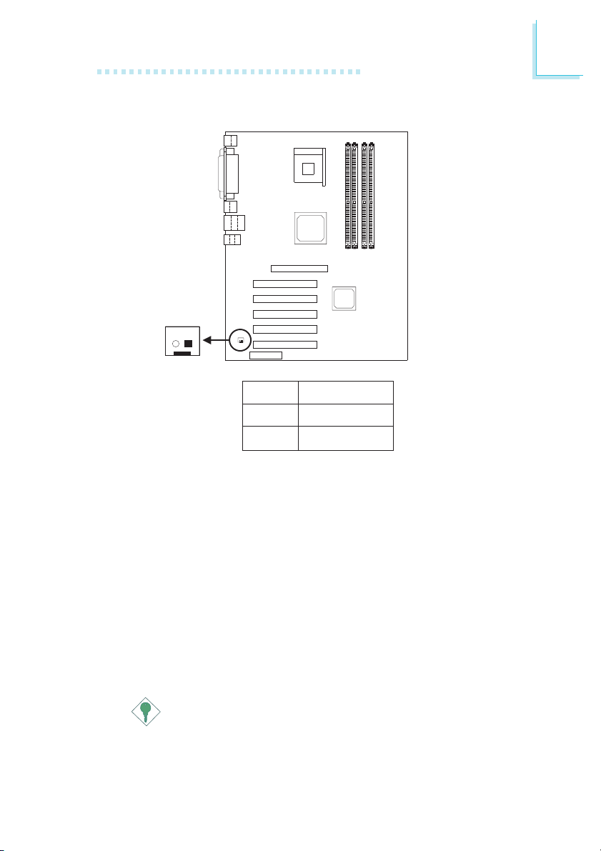
2.13.15 Wake-On-Ring Connector
12
Wake-On-Ring
(J23)
Pin
1
2
Function
Ground
RI#
Hardware Installation
2
The Wake-On-Ring connector is used to connect to an internal
modem add-in card that has the same connector. It will allow the
system that is in the Suspend mode or Soft Power Off mode to
wake-up/power-on to respond to calls coming through the internal
modem card.
To use this function, connect one end of the cable (that came with
the card) to the card’s wake-on-ring connector and the other end to
location J23 on the system board. You must also enable the “Resume
on Ring” field in the Power Management Setup of the BIOS.
If you are using an external modem, the ring-on function will come
through the serial port where the external modem is connected.
Important:
If you are using a modem add-in card, the 5VSB power source
of your power supply must support ≥720mA.
59
Page 60
2
Hardware Installation
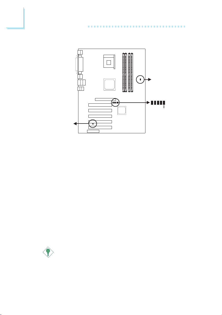
2.13.16 LEDs
DIMM Standby
Power LED
LED 3
LED 2
Warning
PCI Standby
Power LED
AGP Warning LED
The AGP slot suppor ts 1.5V AGP add-in cards. If this type of AGP
card is installed, the AGP Warning LED will not light. However, if no
AGP card is installed in the slot or you installed a +3.3V AGP card,
the LED will light indicating that a non-1.5V card was installed.
LED 4
LED 5
AGP
LED
60
DIMM Standby Power LED
This LED will turn red when the system’s power is on or when it is
in the Suspend state (Power On Suspend or Suspend to RAM). It
will not light when the system is in the Soft-Off state.
PCI Standby Power LED
This LED will turn red when the system is in the power-on, Soft-Off
or Suspend (Power On Suspend or Suspend to RAM) state.
Important:
If the DIMM Standby Power LED or PCI Standby Power LED is
lighted, you must power-off the system then turn off the power
supply’s switch or unplug the power cord prior to installing any
memory modules or add-in cards.
Page 61

Hardware Installation
Diagnostic LEDs
LED 2 to LED 5 are diagnostic LEDs. These LEDs will indicate the
current condition of the system.
2
Early program chipset
register before POST.
Testing memory presence.
Detecting memory size.
No memory present.
Programming DRAM timing
register.
Calculating DRAM size
variable including row,
column and bank.
Initializing JEDEC of current
DRAM row.
Checking CMOS checksum
and battery.
Initializing the clock
generator.
Initializing USB.
LED 2
On
Off
On
Off
On
Off
On
Off
On
Off
LED 3
Off
On
On
Off
Off
On
On
Off
Off
On
LED 4
Off
Off
Off
On
On
On
On
Off
Off
Off
LED 5
Off
Off
Off
Off
Off
Off
Off
On
On
On
Testing all memory (cleared
all extended memory to 0).
Initializing the onboard
Super IO.
Detecting and installing an
IDE device.
Final initialization.
Booting the system.
CPU initially failed.
On
Off
On
Off
Off
On
On
Off
Off
On
Off
On
Off
On
On
On
Off
On
On
On
On
On
Off
On
61
Page 62
2
Hardware Installation
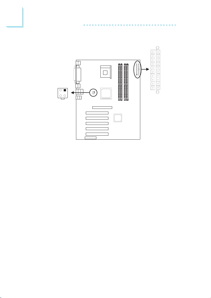
2.13.17 Power Connectors
1
2
3
4
+12V power
10
1
2
4
3
ATX main power
1
(ATXP1)
20
11
(ATXP2)
We recommend that you use a power supply that complies with the
ATX12V Power Supply Design Guide Version 1.1. An ATX12V
power supply has a standard 20-pin ATX main power connector
and a 4-pin +12V power connector that must be inserted onto
ATXP1 and ATXP2 connectors respectively.
The 4-pin +12V power connector enables the delivery of more
+12VDC current to the processor’s Voltage Regulator Module
(VRM).
62
The system board requires a minimum of 250 Watt power supply
to operate. Your system configuration (amount of memory, add-in
cards, peripherals, etc.) may exceed the minimum power requirement.
To ensure that adequate power is provided, use a 300 Watt (or
greater) power supply.
Page 63

Hardware Installation
ATX Main Power Connector
2
Pin
Function
1
3.3V
2
3.3V
3
Ground
4
+5V
5
Ground
6
+5V
7
Ground
8
PW-OK
9
5VSB
10
+12V
+12V Power Connector
Pin
1
2
3
4
Pin
11
12
13
14
15
16
17
18
19
20
Function
Ground
Ground
+12V
+12V
Function
3.3V
-12V
Ground
PS-ON
Ground
Ground
Ground
-5V
+5V
+5V
63
Page 64
2
Hardware Installation
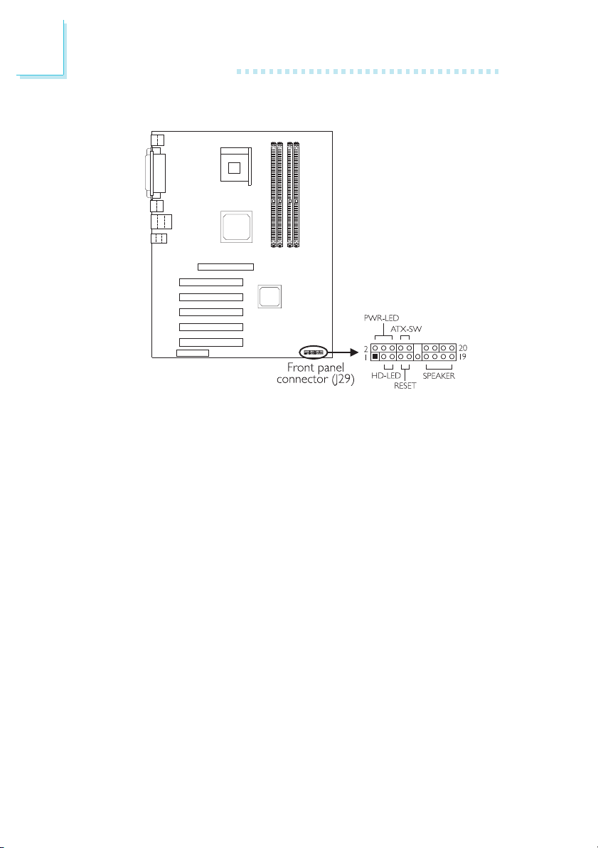
2.13.18 Front Panel Connectors
HD-LED: Primary/Secondary IDE LED
This LED will light when the hard drive is being accessed.
RESET: Reset Switch
This switch allows you to reboot without having to power off the
system thus prolonging the life of the power supply or system.
64
SPEAKER: Speaker Connector
This connects to the speaker installed in the system chassis.
ATX-SW: ATX Power Switch
Depending on the setting in the BIOS setup, this switch is a “dual
function power button” that will allow your system to enter the SoftOff or Suspend mode. Refer to “Soft-Off By PWR-BTTN” in the
Power Management Setup (Chapter 3).
Page 65

Hardware Installation
PWR-LED: Power/Standby LED
When the system’s power is on, this LED will light. When the system
is in the S1 (POS - Power On Suspend) state, it will blink every
second. When the system is in the S3 (STR - Suspend To RAM)
state, it will blink every 4 seconds.
Note:
If a system did not boot-up and the Power/Standby LED did
not light after it was powered-on, it may indicate that the CPU
or memory module was not installed properly. Please make
sure they are properly inserted into their corresponding socket.
Pin
Pin Assignment
HD-LED
(Primary/Secondary IDE LED)
Reserved
ATX-SW
(ATX power switch)
Reserved
RESET
(Reset switch)
SPEAKER
(Speaker connector)
PWR-LED
(Power/Standby LED)
3
HDD LED Power
5
HDD
14
N. C.
16
N. C.
8
PWRBT+
10
PWRBT-
18
N. C.
20
N. C.
7
Ground
9
H/W Reset
13
Speaker Data
15
N. C.
17
Ground
19
Speaker Power
2
LED Power (+)
4
LED Power (+)
6
LED Power (-) or Standby Signal
2
65
Page 66

3
Award BIOS Setup Utility
Chapter 3 - Award BIOS Setup Utility
3.1 The Basic Input/Output System
The Basic Input/Output System (BIOS) is a program that takes care
of the basic level of communication between the processor and
peripherals. In addition, the BIOS also contains codes for various
advanced features found in this system board. This chapter explains
the Setup Utility for the Award BIOS.
After you power up the system, the BIOS message appears on the
screen and the memory count begins. After the memory test, the
following message will appear on the screen:
Press DEL to enter setup
If the message disappears before you respond, restart the system or
press the “Reset” button. You may also restart the system by
pressing the <Ctrl> <Alt> and <Del> keys simultaneously.
When you press <Del>, the main menu screen will appear.
Phoenix - AwardBIOS CMOS Setup Utility
66
Standard CMOS Features
Advanced BIOS Features
Advanced Chipset Features
Integrated Peripherals
Power Management Setup
PnP/PCI Configurations
PC Health Status
: Quit
Esc
: Save & Exit Setup
F10
Time, Date, Hard Disk T ype...
Frequency/Voltage Control
Load Fail-Safe Defaults
Load Optimized Defaults
Set Supervisor Password
Set User Password
Save & Exit Setup
Exit Without Saving
: Select Item
↑↓→←
3.1.1 Standard CMOS Features
Use the arrow keys to highlight “Standard CMOS Features” and
press <Enter>. A screen similar to the one on the next page will
appear.
Page 67

Date (mm:dd:yy)
Time (hh:mm:ss)
X
IDE Primary Master
X
IDE Primary Slave
X
IDE Secondary Master
X
IDE Secondary Slave
Drive A
Drive B
Video
Halt On
Base Memory
Extended Memory
Total Memory
Award BIOS Setup Utility
Phoenix - AwardBIOS CMOS Setup Utility
Standard CMOS Features
Mon, Oct 28 2002
4 : 35 : 5
Press Enter None
Press Enter None
Press Enter None
Press Enter None
1.44M, 3.5 in.
None
EGA/VGA
All, But Keyboard
640K
129024K
130048K
Item Help
Menu Level
Change the day, month,
year and century
3
↑↓→← Move
Enter:Select
F5:Previous Values
+/-/PU/PD:Value
F6:Fail-Safe Defaults F7:Optimized Defaults
F10:Save
ESC:Exit
F1:General Help
The settings on the screen are for reference only. Your version may not be
identical to this one.
3.1.1.1 Date
The date format is <day>, <month>, <date>, <year>. Day displays
a day, from Sunday to Saturday. Month displays the month, from
January to December. Date displays the date, from 1 to 31. Year
displays the year, from 1994 to 2079.
3.1.1.2 Time
The time format is <hour>, <minute>, <second>. The time is based
on the 24-hour military-time clock. For example, 1 p.m. is 13:00:00.
Hour displays hours from 00 to 23. Minute displays minutes from
00 to 59. Second displays seconds from 00 to 59.
3.1.1.3 IDE Primary Master, IDE Primary Slave, IDE Secondary Master
and IDE Secondary Slave
Move the cursor to the “IDE Primary Master”, “IDE Primary Slave”,
“IDE Secondary Master” or “IDE Secondary Slave” field, then press
<Enter>.
67
Page 68

3
Award BIOS Setup Utility
Phoenix - AwardBIOS CMOS Setup Utility
IDE HDD Auto Detection
IDE Primary Master
Access Mode
Capacity
Cylinder
Head
Precomp
Landing Zone
Sector
IDE Primary Master
Press Enter
Auto
Auto
0 M
0
0
0
0
Item Help
Menu Level
Change the day, month,
year and century
↑↓→← :Move
The settings on the screen are for reference only. Your version may not be
identical to this one.
Enter:Select
F5:Previous Values
+/-/PU/PD:Value
F6:Fail-Safe Defaults F7:Optimized Defaults
F10:Save
ESC:Exit
F1:General Help
IDE HDD Auto Detection
Detects the parameters of the drive. The parameters will
automatically be shown on the screen.
IDE Primary Master/Slave and IDE Secondary Master/Slave
If you wish to define your own drive type manually, select “Manual”.
The drive type information should be included in the documentation
from your hard disk vendor. If you select ”Auto”, the BIOS will autodetect the HDD & CD-ROM drive at the POST stage and show
the IDE for the HDD & CD-ROM drive. If a hard disk has not
been installed, select “None”.
Access Mode
For hard drives larger than 528MB, you would typically select the
LBA type. Certain operating systems require that you select Normal
or Large. Please check your operating system’s manual or Help desk
on which one to select.
68
Page 69

Award BIOS Setup Utility
Capacity
Displays the approximate capacity of the disk drive. Usually the size
is slightly greater than the size of a formatted disk given by a disk
checking program.
Cylinder
This field displays the number of cylinders.
Head
This field displays the number of read/write heads.
Precomp
This field displays the number of cylinders at which to change the
write timing.
Landing Zone
This field displays the number of cylinders specified as the landing
zone for the read/write heads.
Sector
3
This field displays the number sectors per track.
3.1.1.4 Drive A and Drive B
These fields identify the types of floppy disk drives installed.
None No floppy drive is installed
360K, 5.25 in. 5-1/4 in. standard drive; 360KB capacity
1.2M, 5.25 in. 5-1/4 in. AT-type high-density drive; 1.2MB capacity
720K, 3.5 in. 3-1/2 in. double-sided drive; 720KB capacity
1.44M, 3.5 in. 3-1/2 in. double-sided drive; 1.44MB capacity
2.88M, 3.5 in. 3-1/2 in. double-sided drive; 2.88MB capacity
69
Page 70

3
Award BIOS Setup Utility
3.1.1.5 Video
This field selects the type of video adapter used for the primary
system monitor. Although secondary monitors are supported, you do
not have to select the type. The default setting is EGA/VGA.
EGA/VGA Enhanced Graphics Adapter/Video Graphics Array. For
EGA, VGA, SVGA and PGA monitor adapters.
CGA 40 Color Graphics Adapter. Power up in 40-column
mode.
CGA 80 Color Graphics Adapter. Power up in 80-column
mode.
Mono Monochrome adapter. Includes high resolution
monochrome adapters.
3.1.1.6 Halt On
This field determines whether the system will stop if an error is
detected during power up. The default setting is All Errors.
No Errors The system boot will not stop for any errors detected.
All Errors The system boot will stop whenever the BIOS detects
a non-fatal error.
All, But Keyboard The system boot will not stop for a keyboard
error; it will stop for all other errors.
All, But Diskette The system boot will not stop for a disk error;
it will stop for all other errors.
All, But Disk/Key The system boot will not stop for a disk or
keyboard error; it will stop for all other errors.
70
3.1.1.7 Base Memory
Displays the amount of base (or conventional) memory installed in
the system. The value of the base memory is typically 512K for
systems with 512K memory installed on the motherboard or 640K
for systems with 640K or more memory installed on the
motherboard.
Page 71

Award BIOS Setup Utility
3.1.1.8 Extended Memory
Displays the amount of extended memory detected during boot-up.
3.1.1.9 Total Memory
Displays the total memory available in the system.
3
71
Page 72

3
Award BIOS Setup Utility
3.1.2 Advanced BIOS Features
The Advanced BIOS Features allows you to configure your system
for basic operation. Some entries are defaults required by the system
board, while others, if enabled, will improve the performance of your
system or let you set some features according to your preference.
Phoenix - AwardBIOS CMOS Setup Utility
Advanced BIOS Features
BIOS Flash Protect
Virus Warning
CPU L1 & L2 Cache
CPU Hyper-Threading
Quick Power On Self Test
RAID or SCSI Card Boot
First Boot Device
Second Boot Device
Third Boot Device
Boot Other Device
Swap Floppy Drive
Boot Up Floppy Seek
Boot Up NumLock Status
Typematic Rate Setting
Typematic Rate (Chars/Sec)
X
Typematic Delay (Msec)
X
Security Option
APIC Mode
MPS Version Control For OS
OS Select For DRAM > 64MB
HDD S.M.A.R.T. Capability
Full Screen Logo Show
↑↓→← Move
Small Logo (EPA) Show
F5:Previous Values
Disabled
Disabled
Enabled
Enabled
Fast
RAID
Floppy
CDROM
HDD-0
Enabled
Disabled
Enabled
On
Disabled
6
250
Setup
Disabled
1.4
Non-OS2
Disabled
Enabled
+/-/PU/PD:Value
Enabled
F6:Fail-Safe Defaults F7:Optimized Defaults
F10:Save
ESC:Exit
The screen above list all the fields available in the Advanced BIOS Features
submenu, for ease of reference in this manual. In the actual CMOS setup,
you have to use the scroll bar to view the fields. The settings on the screen
are for reference only. Your version may not be identical to this one.
Item Help
Menu Level
Allows you to choose
the VIRUS warning
feature for IDE Hard
Disk boot sector
protection. If this
function is enabled and
someone attempt to
write data into this
area, BIOS will show a
warning message on
screen and alarm beep
F1:General HelpEnter:Select
72
3.1.2.1 BIOS Flash Protect
Enabled This option will protect the system from unnecessary
updating or flashing of the BIOS. When enabled, it
secures the BIOS therefore any updates to the BIOS
will not take effect.
Disabled Disables the “BIOS flash protect” function, allowing you
to update or flash the BIOS any time needed.
3.1.2.2 Virus Warning
This field protects the boot sector and partition table of your hard disk
drive. When this field is enabled, the Award BIOS will monitor the boot
sector and partition table of the hard disk drive. If an attempt is made
to write to the boot sector or partition table of the hard disk drive,
the BIOS will halt the system and an error message will appear.
Page 73

Award BIOS Setup Utility
After seeing the error message, if necessary, you will be able to run
an anti-virus program to locate and remove the problem before any
damage is done.
Many disk diagnostic programs which attempt to access the boot
sector table will cause the warning message to appear. If you are
running such a program, we recommend that you first disable this field.
Also, disable this field if you are installing or running certain operating
systems like Windows® 98SE/2000/ME/XP or the operating system
may not install nor work.
3.1.2.3 CPU L1 & L2 Cache
This field speeds up the memory access.
3.1.2.4 CPU Hyper-Threading (for Intel® Pentium® 4 Processor with
Hyper-Threading Technology)
This field is used to enable the functionality of the Intel® Pentium® 4
Processor with Hyper-Threading Technology and will appear only
when using this processor.
3.1.2.5 Quick Power On Self Test
3
This field speeds up Power On Self Test (POST) whenever the
system is powered on. The BIOS will shorten or skip some check
items during POST. To attain the shortest POST time, select “Fast”.
3.1.2.6 RAID or SCSI Card Boot
If you want the system to boot from a drive that is connected to
the RAID IDE connector or SCSI add-in card, you must first select
“SCSI” in the “First Boot Device” field.
If there are drives connected to both the RAID IDE connector and
SCSI add-in card, you must then select which drive you want to
boot.
RAID The drive is connected to the RAID IDE connector
that is on the system board.
SCSI The drive is connected to the SCSI add-in card that is
installed in a PCI slot.
73
Page 74

3
Award BIOS Setup Utility
If the drive is connected to either one of them only, you don’t need
to particularly select an option in this field because the system will
automatically detect for the existing drive.
3.1.2.7 First Boot Device, Second Boot Device, Third Boot Device and
Boot Other Device
Select the drive to boot first, second and third in the “First Boot
Device” “Second Boot Device” and “Third Boot Device” fields
respectively. The BIOS will boot the operating system according to
the sequence of the drive selected. Set “Boot Other Device” to
Enabled if you wish to boot from another device.
3.1.2.8 Swap Floppy Drive
When this field is enabled and the system is booting from the floppy
drive, the system will boot from drive B instead of drive A. When
this field is disabled and the system is booting from the floppy drive,
the system will boot from drive A. You must have two floppy drives
to use this function.
3.1.2.9 Boot Up Floppy Seek
When enabled, the BIOS will check whether the floppy disk drive
installed is 40 or 80 tracks. Note that the BIOS cannot distinguish
between 720K, 1.2M, 1.44M and 2.88M drive types as they are all 80
tracks. When disabled, the BIOS will not search for the type of floppy
disk drive by track number. Note that there will not be any warning
message if the drive installed is 360KB.
74
3.1.2.10 Boot Up NumLock Status
This allows you to determine the default state of the numeric
keypad. By default, the system boots up with NumLock on wherein
the function of the numeric keypad is the number keys. When set to
Off, the function of the numeric keypad is the arrow keys.
Page 75

Award BIOS Setup Utility
3.1.2.11 Typematic Rate Setting
Disabled Continually holding down a key on your keyboard will
cause the BIOS to report that the key is down.
Enabled The BIOS will not only report that the key is down,
but will first wait for a moment, and, if the key is still
down, it will begin to repor t that the key has been
depressed repeatedly. For example, you would use such
a feature to accelerate cursor movements with the
arrow keys. You can then select the typematic rate and
typematic delay in the “Typematic Rate (Chars/Sec)”
and “Typematic Delay (Msec)” fields below.
3.1.2.12 Typematic Rate (Chars/Sec)
This field allows you to select the rate at which the keys are
accelerated.
3.1.2.13 Typematic Delay (Msec)
This field allows you to select the delay between when the key was
first depressed and when the acceleration begins.
3.1.2.14 Security Option
3
This field determines when the system will prompt for the password
- everytime the system boots or only when you enter the BIOS
setup. Set the password in the Set Supervisor/User Password
submenu.
System The system will not boot and access to Setup will be
denied unless the correct password is entered at the
prompt.
Setup The system will boot, but access to Setup will be denied
unless the correct password is entered at the prompt.
75
Page 76

3
Award BIOS Setup Utility
3.1.2.15 APIC Mode
Leave this field in its default setting.
3.1.2.16 MPS Version Control for OS
This field is used to select the MPS version that the system board is
using.
3.1.2.17 OS Select for DRAM > 64MB
This field allows you to access the memory that is over 64MB in
OS/2.
3.1.2.18 HDD S.M.A.R.T. Capability
The system board supports SMART (Self-Monitoring, Analysis and
Reporting Technology) hard drives. SMART is a reliability prediction
technology for ATA/IDE and SCSI drives. The drive will provide
sufficient notice to the system or user to backup data prior to the
drive’s failure. The default is Disabled. If you are using hard drives
that support S.M.A.R.T., set this field to Enabled. SMART is
supported in ATA/33 or later hard drives.
76
3.1.2.19 Full Screen Logo Show
This field is applicable only if you want a particular logo to appear
during system boot-up.
Enabled The logo will appear in full screen during system boot-
up.
Disabled The logo will not appear during system boot-up.
3.1.2.20 Small Logo(EPA) Show
Enabled The EPA logo will appear during system boot-up.
Disabled The EPA logo will not appear during system boot-up.
Page 77

3.1.3 Advanced Chipset Features
Phoenix - AwardBIOS CMOS Setup Utility
Advanced Chipset Features
DRAM Timing Selectable
CAS Latency Time
X
Active to Precharge Delay
X
DRAM RAS# to CAS# Delay
X
DRAM RAS# Precharge
X
DRAM Read Thermal Mgmt
Buffer Strength Control
System BIOS Cacheable
Video BIOS Cacheable
Delayed Transaction
Delay Prior to Thermal
AGP Aperture Size (MB)
AGP 4X Mode
By SPD
3
7
3
3
Disabled
Press Enter
Disabled
Disabled
Enabled
16 Min
64
Enabled
Award BIOS Setup Utility
Item Help
Menu Level
3
↑↓→← Move
F5:Previous Values
+/-/PU/PD:Value F10:Save ESC:Exit
F6:Fail-Safe Defaults F7:Optimized Defaults
F1:General HelpEnter:Select
The settings on the screen are for reference only. Your version may not be
identical to this one.
This section gives you functions to configure the system based on
the specific features of the chipset. The chipset manages bus speeds
and access to system memory resources. These items should not
be altered unless necessary. The default settings have been chosen
because they provide the best operating conditions for your system.
The only time you might consider making any changes would be if
you discovered some incompatibility or that data was being lost
while using your system.
3.1.3.1 DRAM Timing Selectable
This field is used to select the timing of the DRAM.
By SPD The EEPROM on a DIMM has SPD (Serial Presence
Detect) data structure that stores information about
the module such as the memory type, memory size,
memory speed, etc. When this option is selected,
the system will run according to the information in
the EEPROM. This option is the default setting
because it provides the most stable condition for
the system. The “CAS Latency Time” to “DRAM
RAS# Precharge” fields will show the default settings
by SPD.
77
Page 78

3
Award BIOS Setup Utility
By User If you want better system performance other than
the one “by SPD”, select “By User”. Then select the
best option in the “CAS Latency Time” to “DRAM
RAS# Precharge” fields.
3.1.3.2 CAS Latency Time
This field is used to select the local memory clock periods.
3.1.3.3 Active to Precharge Delay
The options are 5, 6 and 7.
3.1.3.4 DRAM RAS# to CAS# Delay
The options are 2 and 3.
3.1.3.5 DRAM RAS# Precharge
This field controls RAS# precharge (in local memory clocks).
3.1.3.6 DRAM Read Thermal Mgmt
This field is used to detect the DDR’s thermal condition.
78
3.1.3.7 Buffer Strength Control
Leave this in its default setting.
3.1.3.8 System BIOS Cacheable
When this field is enabled, accesses to the system BIOS ROM
addressed at F0000H-FFFFFH are cached, provided that the cache
controller is enabled. The larger the range of the Cache RAM, the
higher the efficiency of the system.
3.1.3.9 Video BIOS Cacheable
As with caching the system BIOS, enabling the Video BIOS cache will
allow access to video BIOS addresssed at C0000H to C7FFFH to
be cached, if the cache controller is also enabled. The larger the range
of the Cache RAM, the faster the video performance.
Page 79

Award BIOS Setup Utility
3.1.3.10 Delayed Transaction
When enabled, this function frees up the PCI bus for other PCI
masters during the PCI-to-ISA transactions. This allows PCI and ISA
buses to be used more efficiently and prevents degradation of
performance on the PCI bus when ISA accesses are made.
3.1.3.11 Delay Prior to Thermal
The default is 16 Min.
3.1.3.12 AGP Aperture Size (MB)
This field is relevant to the memory-mapped graphics data of the
AGP card installed in your system. Leave this in its default setting.
3.1.3.13 AGP 4X Mode
This field is used to enable the AGP 4x interface which transfers video
data at 1066MB/sec. bandwidth thus delivering faster and better
graphics to your PC. Make sure your graphics card supports the AGP
4x mode.
3
79
Page 80

3
Award BIOS Setup Utility
3.1.4 Integrated Peripherals
Phoenix - AwardBIOS CMOS Setup Utility
Integrated Peripherals
X
INTEL OnChip IDE Device
X
INTEL OnChip PCI Device
X
Onboard Super IO Device
USB Controller
USB Keyboard Support
USB Mouse Support
Init Display First
Press Enter
Press Enter
Press Enter
USB 2.0 Disabled
Disabled
Disabled
AGP
Item Help
Menu Level
↑↓→← Move
F5:Previous Values
+/-/PU/PD:Value
F6:Fail-Safe Defaults F7:Optimized Defaults
F10:Save
ESC:Exit
F1:General HelpEnter:Select
The settings on the screen are for reference only. Your version may not be
identical to this one.
3.1.4.1 INTEL OnChip IDE Device
Move the cursor to this field and press <Enter>. The following
screen will appear.
Phoenix - AwardBIOS CMOS Setup Utility
INTEL OnChip IDE Device
On-Chip Primary PCI IDE
IDE Primary Master PIO
IDE Primary Slave PIO
IDE Primary Master UDMA
IDE Primary Slave UDMA
On-Chip Secondary PCI IDE
IDE Secondary Master PIO
IDE Secondary Slave PIO
IDE Secondary Master UDMA
IDE Secondary Slave UDMA
IDE HDD Block Mode
↑↓→← Move
F5:Previous Values
Enabled
Auto
Auto
Auto
Auto
Enabled
Auto
Auto
Auto
Auto
Enabled
+/-/PU/PD:Value
F6:Fail-Safe Defaults F7:Optimized Defaults
F10:Save
ESC:Exit
The settings on the screen are for reference only. Your version may not be
identical to this one.
Item Help
Menu Level
F1:General HelpEnter:Select
80
Page 81

Award BIOS Setup Utility
On-Chip Primary PCI IDE and On-Chip Secondary PCI IDE
These fields allow you to enable or disable the primary and
secondary IDE controller. Select Disabled if you want to add a
different hard drive controller.
IDE Primary Master/Slave PIO and IDE Secondary Master/Slave
PIO
PIO means Programmed Input/Output. Rather than have the BIOS
issue a series of commands to effect a transfer to or from the disk
drive, PIO allows the BIOS to tell the controller what it wants and
then let the controller and the CPU perform the complete task by
themselves. Your system supports five modes, 0 (default) to 4, which
primarily differ in timing. When Auto is selected, the BIOS will select
the best available mode after checking your drive.
Auto The BIOS will automatically set the system according
to your hard disk drive’s timing.
Mode 0-4 You can select a mode that matches your hard disk
drive’s timing. Caution: Do not use the wrong setting
or you will have drive errors.
IDE Primary Master/Slave UDMA and IDE Secondary Master/
Slave UDMA
3
These fields allow you to set the Ultra DMA in use. When Auto is
selected, the BIOS will select the best available option after checking
your hard drive or CD-ROM.
Auto The BIOS will automatically detect the settings for
you.
Disabled The BIOS will not detect these categories.
IDE HDD Block Mode
Enabled The IDE HDD uses the block mode. The system
BIOS will check the hard disk drive for the
maximum block size the system can transfer. The
block size will depend on the type of hard disk
drive.
Disabled The IDE HDD uses the standard mode.
81
Page 82

3
Award BIOS Setup Utility
3.1.4.2 INTEL OnChip PCI Device
Move the cursor to this field and press <Enter>. The following
screen will appear.
Phoenix - AwardBIOS CMOS Setup Utility
INTEL OnChip PCI Device
AC97 Audio
AC97 Modem
CNR LAN Control
Onboard AC97 Codec
Onboard LAN Control
Auto
Auto
Disabled
Enabled
Enabled
Item Help
Menu Level
↑↓→← Move
The settings on the screen are for reference only. Your version may not be
identical to this one.
F5:Previous Values
+/-/PU/PD:Value
F6:Fail-Safe Defaults F7:Optimized Defaults
F10:Save
ESC:Exit
F1:General HelpEnter:Select
AC97 Audio
Auto Select this option when using the onboard audio
codec, primary or secondar y audio riser card, or
audio/modem riser card.
Disabled Select this option when using a PCI sound card.
AC97 Modem
Auto Select this option when using a primary or
secondary modem riser card, or audio/modem riser
card.
Disabled Select this option when using a PCI modem card.
CNR LAN Control
Auto Select this option to use the LAN CNR board that
is installed in the CNR slot.
Disabled Select this option to disable the LAN CNR board
that is installed in the CNR slot.
82
Page 83

Award BIOS Setup Utility
Onboard AC97 Codec
Enabled Select this option to enable the onboard AC97
codec.
Disabled Select this option to disable the onboard AC97
codec. Disable the onboard AC97 codec when
using a 6-channel audio CNR card or an audio PCI
card.
Onboard LAN Control
This field is used to enable or disable the Realtek RTL8100 LAN
chip.
3
83
Page 84

3
Award BIOS Setup Utility
3.1.4.3 Onboard Super IO Device
Move the cursor to this field and press <Enter>. The following
screen will appear.
Phoenix - AwardBIOS CMOS Setup Utility
Onboard Super IO Device
KBC Input Clock
Keyboard/Mouse Power On
KB Power ON Password
KB Power ON Hot Key
Onboard FDC Controller
SCR Port Address/IRQ
MS/SD Port Address/IRQ
MS/SD Port Mode
Onboard Serial Port 1
Onboard Serial Port 2
UART2 Mode Select
RxD, TxD Active
X
IR Transmission Delay
X
UR2 Duplex Mode
X
Use IR Pins
X
Onboard Parallel Port
Parallel Port Mode
EPP Mode Select
ECP Mode Use DMA
PWR Lost Resume State
Game Port Address
Midi Port Address
↑↓→← Move
Midi Port IRQ
F5:Previous Values
The screen above list all the fields available in the Onboard Super IO
Device submenu, for ease of reference in this manual. In the actual CMOS
12MHz
Disabled
Enter
Ctrl-F1
Enabled
Disabled
Disabled
MS Socket
3F8/IRQ4
2F8/IRQ3
Normal
Hi,Lo
Enabled
Half
IR-Rx2Tx2
378/IRQ7
ECP+EPP
EPP 1.7
3
Keep Off
201
Disabled
+/-/PU/PD:Value F10:Save ESC:Exit
10X
F6:Fail-Safe Defaults F7:Optimized Defaults
setup, you have to use the scroll bar to view the fields. The settings on the
screen are for reference only. Your version may not be identical to this one.
Item Help
Menu Level
F1:General HelpEnter:Select
84
KBC Input Clock
This is used to select the input clock of your keyboard.
Keyboard/Mouse Power On
This field allows you to use the keyboard or PS/2 mouse to poweron the system. To use this function, make sure JP1 is set to 2-3 On the Wake-On-Keyboard/Mouse function enabled. Refer to “Jumper
Settings for Wake-On-Keyboard/Wake-On-Mouse” in chapter 2 for
more information.
Disabled Default setting.
.
.
.
.
.
Warning:
.
.
.
If JP1 was previously enabled with a password set in the “KB Power On Password” field,
and now you wish to disable the keyboard
password function, make sure to set this field
to disabled prior to setting JP1 to disabled
Page 85

Award BIOS Setup Utility
(1-2 On). You will not be able to boot up the
system if you fail to do so.
Password When this option is selected, move the cursor to
the “KB Power On Password” field and press
<Enter>. Enter your password. You can enter up to
5 characters. Type in exactly the same password to
confirm, then press <Enter>.
Important:
The power button will not function once a
keyboard password has been set in the “KB
Power On Password” field. You must type the
correct password to power-on the system. If
you forgot the password, power-off the
system and remove the battery. Wait for a
few seconds and install it back before
powering-on the system.
Hot Key When this option is selected, move the cursor to
the “KB Power On Hot Key” field to select a
function key you would like to use to power-on the
system. The options are from Ctrl-F1 to Ctrl-F12.
Mouse Left When this option is selected, double-click the left
button of the mouse to power-on the system.
Mouse Right When this option is selected, double-click the right
button of the mouse to power-on the system.
Any Key Press any key to power-on the system.
Keyboard 98 When this option is selected, press the “wake up”
key of the Windows 98 compatible keyboard to
power-on the system.
3
Onboard FDC Controller
Enabled Enables the onboard floppy disk controller.
Disabled Disables the onboard floppy disk controller.
SCR Port Address/IRQ
This field is used to select the SC port’s IRQ. The number that
appears before the IRQ selected is the SC por t’s address.
85
Page 86

3
Award BIOS Setup Utility
MS/SD Port Address/IRQ
This field is used to select the MS or SD port’s IRQ. The number
that appears before the IRQ selected is the MS/SD port’s address.
Important:
IRQs for Serial Port 1, Serial Port 2, Parallel Port, SC Port and
MS/SD Port must be appropriately selected making sure each
port uses a different IRQ. For example, if you selected “700H/
IRQ3” for the SC port, “700H” is the port’s address and
“IRQ3” is the IRQ. Therefore you must not select IRQ3 for the
other ports.
MS/SD Port Mode
The MS/SD connector (JP8) is an interface for Memory Stick or
Secure Digital Memory Card.
MS Socket Select this option if JP8 connects to the Memory
Stick socket.
SD Socket Select this option if JP8 connects to the Secure
Digital Memory Card socket.
Onboard Serial Port 1 and Onboard Serial Port 2
86
Auto The system will automatically select an I/O address
for the onboard serial port 1 and serial port 2.
3F8/IRQ4, 2F8/IRQ3, 3E8/IRQ4, 2E8/IRQ3 Allows you to
manually select an I/O address for the onboard
serial port 1 and serial por t 2.
Disabled Disables the onboard serial port 1 and/or serial
port 2.
Page 87

Award BIOS Setup Utility
UART2 Mode Select
The system board supports IrDA function for wireless connectivity
between your computer and peripheral devices. You may not use
IrDA (J24) and the COM 2 serial port (CN3) at the same time. If
you are using the COM 2 serial port, make sure this field is set to
Normal.
To use the IrDA function, follow the steps below.
1. Connect your IrDA cable to connector J24 on the system board.
2. Set the “UART2 Mode Select” field to the type of IrDA standard
supported by your IrDA peripheral/device (IrDA or ASKIR). For
better transmission of data, your IrDA peripheral device must be
within a 30o angle and within a distance of 1 meter.
3. Set the “RxD, TxD Active” and “Use IR Pins” fields appropriately.
RxD, TxD Active
The options are Hi, Lo; Lo, Hi; Lo, Lo; and Hi, Hi.
IR Transmission Delay
3
If this field is Enabled, transmission of data will be slower. This is
recommended when you encounter transmission problem with your
device.
UR2 Duplex Mode
Half Data is completely transmitted before receiving data.
Full Transmits and receives data simultaneously.
Use IR Pins
The options are IR-Rx2Tx2 and RxD2TxD2.
Onboard Parallel Port
378/IRQ7, 3BC/IRQ7, 278/IRQ5 Selects the I/O address and
IRQ for the onboard parallel port.
Disabled Disables the onboard parallel port.
87
Page 88

3
Award BIOS Setup Utility
Parallel Port Mode
The options are SPP, EPP, ECP, ECP+EPP and PntMode. These apply
to a standard specification and will depend on the type and speed
of your device. Refer to your peripheral’s manual for the best option.
SPP
Allows normal speed operation but in one direction only.
ECP (Extended Capabilities Port)
Allows parallel port to operate in bidirectional mode and at a
speed faster than the normal mode’s data transfer rate.
EPP (Enhanced Parallel Port)
Allows bidirectional parallel port operation at maximum speed.
PntMode
Allows parallel port to operate in bipolar mode.
If you selected EPP, the “EPP Mode Select” field is configurable. If you
selected ECP, the “ECP Mode Use DMA” field is configurable. If you
selected ECP+EPP, both “EPP Mode Select” and “ECP Mode Use
DMA” are configurable.
88
EPP Mode Select
This is used to select the EPP mode.
ECP Mode Use DMA
This is used to select the DMA channel of the parallel port.
PWR Lost Resume State
Keep Off When power returns after an AC power failure, the
system’s power is off. You must press the Power
button to power-on the system.
Tur n On When power returns after an AC power failure, the
system will automatically power-on.
Last State When power returns after an AC power failure, the
system will return to the state where you left off
before power failure occurs. If the system’s power is
off when AC power failure occurs, it will remain off
Page 89

Award BIOS Setup Utility
when power returns. If the system’s power is on
when AC power failure occurs, the system will poweron when power returns.
Game Port Address
This field is used to select the game port’s address.
Midi Port Address
This field is used to select the midi port’s address. If you have
selected the midi port’s address, you may select its IRQ in the “Midi
Port IRQ” field.
Midi Port IRQ
This field is used to select the midi port’s IRQ.
3.1.4.4 USB Controller
All Enabled Enables all USB ports.
USB 2.0 Disabled USB 2.0 is disabled; USB 1.1 is enabled.
All Disabled Disables all USB ports.
3.1.4.5 USB Keyboard Support
3
If you are using a USB keyboard under DOS, set this field to
Enabled. This field can be configured only if the “USB Controller” field
is enabled.
3.1.4.6 USB Mouse Support
This field is used to enable or disable the USB mouse. It can be
configured only if the “USB Controller” field is enabled.
3.1.4.7 Init Display First
This field is used to select whether to initialize the AGP or PCI first
when the system boots.
AGP When the system boots, it will first initialize the
AGP.
PCI Slot When the system boots, it will first initialize PCI.
89
Page 90

3
Award BIOS Setup Utility
3.1.5 Power Management Setup
The Power Management Setup allows you to configure your system
to most effectively save energy.
Phoenix - AwardBIOS CMOS Setup Utility
Power Management Setup
ACPI Function
ACPI Suspend Type
Power Management
Video Off Method
Video Off In Suspend
Suspend Mode
HDD Power Down
Soft-Off By PWR-BTTN
Resume on PCI Event
Resume on Ring
Resume on LAN
USB KB Wake-Up From S3
X
Resume by Alarm
Date(of Month) Alarm
X
Time (hh:mm:ss) Alarm
X
Enabled
S1(POS)
User Define
V/H SYNC+Blank
Yes
Disabled
Disabled
Instant-Off
Disabled
Disabled
Disabled
Disabled
Disabled
0
0 : 0 : 0
Item Help
Menu Level
↑↓→← Move
F5:Previous Values
+/-/PU/PD:Value
F6:Fail-Safe Defaults F7:Optimized Defaults
F10:Save
ESC:Exit
F1:General HelpEnter:Select
The settings on the screen are for reference only. Your version may not be
identical to this one.
3.1.5.1 ACPI Function
This function should be enabled only in operating systems that
®®
®
support ACPI. Currently, only Windows
®®
98SE/2000/ME/XP
supports this function. When this field is enabled, the system will
ignore the settings in the “Suspend Mode” and “HDD Power Down”
fields. If you want to use the Suspend to RAM function, make sure
this field is enabled then select “S3(STR)” in the field below.
3.1.5.2 ACPI Suspend Type
This field is used to select the type of Suspend mode.
S1(POS) Enables the Power On Suspend function.
S3(STR) Enables the Suspend to RAM function.
90
Page 91

Award BIOS Setup Utility
3.1.5.3 Power Management
This field allows you to select the type (or degree) of power saving
by changing the length of idle time that elapses before the HDD
Power Down field is activated.
Min Saving Minimum power saving time for the HDD Power
Down = 15 min.
Max Saving Maximum power saving time for the HDD Power
Down = 1 min.
User Define Allows you to set the power saving time in the
“HDD Power Down” field.
3.1.5.4 Video Off Method
This determines the manner in which the monitor is blanked.
V/H SYNC + Blank This selection will cause the system to turn
off the vertical and horizontal synchronization
ports and write blanks to the video buffer.
Blank Screen This option only writes blanks to the video buffer.
DPMS Initializes display power management signaling. Use
this option if your video board supports it.
3
3.1.5.5 Video Off In Suspend
This field is used to activate the video off feature when the system
enters the Suspend mode.
3.1.5.6 Suspend Mode
When the system enters the Suspend mode, the CPU and onboard
peripherals will be shut off.
3.1.5.7 HDD Power Down
This is selectable only when the Power Management field is set to
User Define. When the system enters the HDD Power Down mode
according to the power saving time selected, the hard disk drive will
be powered down while all other devices remain active.
91
Page 92

3
Award BIOS Setup Utility
3.1.5.8 Soft-Off by PWR-BTTN
This field allows you to select the method of powering off your
system.
Hold 4 Sec. Regardless of whether the Power Management
function is enabled or disabled, if the power button
is pushed and released in less than 4 sec, the
system enters the Suspend mode. The purpose of
this function is to prevent the system from powering
off in case you accidentally “hit” or pushed the
power button. Push and release again in less than 4
sec to restore. Pushing the power button for more
than 4 seconds will power off the system.
Instant-Off Pressing and then releasing the power button at
once will immediately power off your system.
3.1.5.9 Resume on PCI Event
Enabled Access to the onboard LAN or a PCI card such as a
modem or LAN card will cause the system to wake up.
The PCI card must support the wake up function.
Disabled The system will not wake up despite access to the PCI
card.
92
3.1.5.10 Resume On Ring
Set this field to Enabled to use the modem ring-on function. This will
allow your system to power-on to respond to calls coming through
an external or internal modem. Refer to “Wake-On-Ring Connector”
in chapter 2 for more information.
3.1.5.11 Resume On LAN
If you are using a LAN card that supports the remote wake up
function, set this field to Enabled. The will allow the network to
remotely wake up a Soft Power Down (Soft-Off) PC. However, if
your system is in the Suspend mode, you can wake up the system
only through an IRQ or DMA interrupt. Refer to “Wake-On-LAN
Connector” in chapter 2 for more information.
Page 93

Award BIOS Setup Utility
3.1.5.12 USB KB Wake-Up From S3
This field, when enabled, allows you to use a USB keyboard to wake
up a system from the S3 (STR - Suspend To RAM) state. This can be
configured only if the “ACPI Suspend Type” field is set to “S3(STR)”.
3.1.5.13 Resume By Alarm
Enabled When Enabled, you can set the date and time you
would like the Soft Power Down (Soft-Off) PC to
power-on in the “Date (of Month) Alarm” and “Time
(hh:mm:ss) Alarm” fields. However, if the system is being
accessed by incoming calls or the network (Resume On
Ring/LAN) prior to the date and time set in these
fields, the system will give priority to the incoming calls
or network.
Disabled Disables the automatic power-on function. (default)
3.1.5.14 Date (of Month) Alarm
0 The system will power-on everyday according to the
time set in the “Time (hh:mm:ss) Alarm” field.
1-31 Select a date you would like the system to power-on.
The system will power-on on the set date, and time set
in the “Time (hh:mm:ss) Alarm” field.
3
3.1.5.15 Time (hh:mm:ss) Alarm
This is used to set the time you would like the system to power-on.
If you want the system to power-on everyday as set in the “Date
(of Month) Alarm” field, the time set in this field must be later than
the time of the RTC set in the Standard CMOS Features submenu.
93
Page 94

3
Award BIOS Setup Utility
3.1.6 PnP/PCI Configurations
This section describes configuring the PCI bus system. It covers
some very technical items and it is strongly recommended that only
experienced users should make any changes to the default settings.
Phoenix - AwardBIOS CMOS Setup Utility
PnP/PCI Configurations
Reset Configuration Data
Resources Controlled By
IRQ Resources
X
PCI/VGA Palette Snoop
* PCI IRQ Assignment *
Slot 1,5
Onboard AC97/Slot 2
Slot 3
Onboard USB/Slot 4
Disabled
Auto(ESCD)
Press Enter
Disabled
Auto
Auto
Auto
Auto
Item Help
Menu Level
Default is Disabled.
Select Enabled to
reset Extended System
Configuration Data
(ESCD) when you exit
Setup if you have
installed a new add-on
and the system
reconfiguration has
caused such a serious
conflict that the OS
cannot boot.
94
↑↓→← Move
F5:Previous Values
+/-/PU/PD:Value
F6:Fail-Safe Defaults F7:Optimized Defaults
F10:Save
ESC:Exit
F1:General HelpEnter:Select
The settings on the screen are for reference only. Your version may not be
identical to this one.
3.1.6.1 Reset Configuration Data
Enabled The BIOS will reset the Extended System Configuration
Data (ESCD) once automatically. It will then recreate a
new set of configuration data.
Disabled The BIOS will not reset the configuration data.
3.1.6.2 Resources Controlled By
The Award Plug and Play BIOS has the capability to automatically
configure all of the boot and Plug and Play compatible devices.
Auto(ESCD) The system will automatically detect the settings for
you.
Manual Choose the specific IRQ in the “IRQ Resources”
field.
Page 95

Award BIOS Setup Utility
3.1.6.3 IRQ Resources
This field is used to set each system interrupt to either “PCI Device”
or “Reserved”.
3.1.6.4 PCI/VGA Palette Snoop
This field determines whether the MPEG ISA/VESA VGA cards can
work with PCI/VGA or not.
Enabled MPEG ISA/VESA VGA cards work with PCI/VGA.
Disabled MPEG ISA/VESA VGA cards does not work with PCI/
VGA.
3.1.6.5 PCI IRQ Assignment
By default, an IRQ is automatically assigned to the PCI devices that
are installed in the PCI slots. If a PCI device has not been assigned
an IRQ, you must manually assign an IRQ for the device. During
system boot-up, you will see “NA” for the device that does not
have an IRQ assigned.
3
95
Page 96

3
Award BIOS Setup Utility
3.1.7 PC Health Status
Phoenix - AwardBIOS CMOS Setup Utility
Shutdown Temperature
Current System Temp.
Current CPU Temperature
Current CPU FAN Speed
Current System FAN Speed
Vcore :
+3.3 V :
+5 V :
+12 V :
VBAT (V) :
5VSB (V) :
↑↓→← Move
The settings on the screen are for reference only. Your version may not be
identical to this one.
F5:Previous Values
PC Health Status
75oC/167oF
27oC/80oF
40oC/66oF
0 RPM
0 RPM
2.06 V
3.31 V
5.05 V
12.03 V
3.21 V
5.40 V
+/-/PU/PD:Value
F6:Fail-Safe Defaults F7:Optimized Defaults
F10:Save
Menu Level
ESC:Exit
Item Help
F1:General HelpEnter:Select
3.1.7.1 Shutdown Temperature
To prevent system overheat, select a temperature that would shutdown
the system. If the system detected that its temperature exceeded the
one set in this field, the system will automatically shutdown.
Note:
The onboard hardware monitor function is capable of detecting
“system health” conditions but if you want a warning message
to pop-up or a warning alarm to sound when an abnormal
condition occurs, you must install the Hardware Monitor utility.
This utility is included in the CD that came with the system
board. Refer to the Hardware Monitor section in chapter 4 for
more information.
96
3.1.7.2 Current System Temperature, Current CPU Temperature,
Current CPU Fan Speed and Current System Fan Speed
These fields show the internal temperature of the system, current
temperature of the CPU and the current fan speed of the CPU and
system fans in RPM (Revolutions Per Minute).
Page 97

Award BIOS Setup Utility
3.1.7.3 Vcore
This field shows the voltage of the processor.
3.1.7.4 +3.3V, +5V, +12V, VBAT (V) and 5VSB (V)
These fields show the output voltage of the power supply.
3
97
Page 98
3
Award BIOS Setup Utility
3.1.8 Frequency/Voltage Control
CMOS Setup Utility - Copyright (C) 1984-2000 Award Software
CPU Clock Ratio
CPU Vcore Adjust
Auto Detect PCI Clk
Spread Spectrum Modulated
Clock By Slight Adjust
PCI/AGP Clock Adjust
↑↓→← Move
The settings on the screen are for reference only. Your version may not be
identical to this one.
Enter:Select
F5:Previous Values
Frequency/Voltage Control
8 X
Default
Enabled
Enabled
100MHz
Auto
+/-/PU/PD:Value
F6:Fail-Safe Defaults
F10:Save
3.1.8.1 CPU Clock Ratio
This field is used to select the frequency ratio of the processor.
Important:
The frequency ratio of some processors may have been locked
by the manufacturer. If you are using this kind of processor,
setting an extended ratio for the processor will have no effect.
The system will instead use its factory default ratio.
Item Help
Menu Level
F1:General HelpESC:Exit
F7:Optimized Defaults
98
3.1.8.2 CPU Vcore Adjust
This field allows you to manually select higher core voltage supplied
to the CPU. If you wish to use the CPU’s default core voltage, leave
this field in its default setting, which is “Default”. The CPU’s Vcore will
be generated according to the CPU VID configuration.
Important:
Although this function is supported, we do not recommend that
you use a higher voltage because unstable current may be
supplied to the system board causing damage.
Page 99

Award BIOS Setup Utility
3.1.8.3 Auto Detect PCI Clk
When enabled, the system will automatically send clock signals to
existing PCI devices.
3.1.8.4 Spread Spectrum
Leave this field in its default setting. Do not alter this setting unless
advised by an engineer or technician.
3.1.8.5 Clock By Slight Adjust
This field provides several options for selecting the external system
bus clock of the processor. The available options allow you to adjust
the processor’s bus clock by 1MHz increment.
Important:
Selecting an external bus clock other than the default setting
may result to the processor’s or system’s instability and are not
guaranteed to provide better system performance.
If you selected an option other than the default setting and is unable
to boot up the system, there are 2 methods of booting up the
system and going back to its default setting.
3
Method 1:
Clear the CMOS data by setting JP5 to 2-3 On. All fields in the
BIOS Setup will automatically be set to their default settings.
Method 2:
Press the <Insert> key and power button simultaneously, then
release the power button first. Keep-on pressing the <Insert> key
until the power-on screen appears. This will allow the system to boot
according to the FSB of the processor. Now press the <Del> key
to enter the main menu of the BIOS. Select “Frequency/Voltage
Control” and set the “CPU Clock Ratio” or “Clock By Slight Adjust”
field to its default setting or an appropriate frequency ratio or bus
clock.
Note:
Use a PS/2 or AT (requires a DIN to mini DIN adapter)
keyboard for method 2.
99
Page 100

3
Award BIOS Setup Utility
3.1.8.6 PCI/AGP Clock Adjust
This field is used to select the AGP clock. The number that appeared
before the AGP clock is its corresponding PCI clock. For example, if
you selected “33/66 MHz”, 66MHz is the AGP clock and 33MHz is
the PCI clock.
3.1.9 Load Fail-Safe Defaults
The “Load Fail-Safe Defaults” option loads the troubleshooting
default values permanently stored in the ROM chips. These settings
are not optimal and turn off all high performance features. You
should use these values only if you have hardware problems.
Highlight this option in the main menu and press <Enter>. The
message below will appear.
Load Fail-Safe Defaults (Y/N)? N
If you want to proceed, type <Y> and press <Enter>. The default
settings will be loaded.
3.1.10 Load Optimized Defaults
The “Load Optimized Defaults” option loads optimized settings from
the BIOS ROM. Use the default values as standard values for your
system. Highlight this option in the main menu and press <Enter>.
The message below will appear.
100
Load Optimized Defaults (Y/N)? N
Type <Y> and press <Enter> to load the Setup default values.
 Loading...