

DFI G586VPA, G586VPB User Manual

G586VPB
Rev. 0
System Board
User’s Manual
- D26850410 -

v Copyright 1995 by DFI, Inc.
All rights reserved.
No part of this document may be copied, reproduced in
any form or by any means or used to make any transformation/adaptation without the prior written consent
of DFI, Inc.
DFI, Inc. makes no warranties with respect to this
documentation and disclaims any implied warranties of
merchantability, quality, or fitness for any particular
purpose. The information in this document is subject to
change without notice. DFI, Inc. reserves the right to
make revisions to this publication and to make changes
to any and/or all parts of its content, at any time,
without obligation to notify any person or entity of such
changes. Further, DFI, Inc. assumes no responsibility
for any errors that may appear in this document.
DFI is a registered trademark, and G586VPB is a
trademark of Diamond Flower, Inc. All other product
names mentioned are trademarks or registered trademarks of their respective companies.

v FCC Statement on Class B
This equipment has been tested and found to comply
with the limits for a Class B digital device, pursuant to
Part 15 of the FCC rules. These limits are designed to
provide reasonable protection against harmful interference when the equipment is operated in a residential
installation. This equipment generates, uses and can
radiate radio frequency energy and, if not installed and
used in accordance with the instruction manual, may
cause harmful interference to radio communications.
However, there is no guarantee that interference will
not occur in a particular installation. If this equipment
does cause harmful interference to radio or television
reception, which can be determined by turning the
equipment off and on, the user is encouraged to try to
correct the interference by one or more of the following
measures:
• Reorient or relocate the receiving antenna.
• Increase the separation between the equipment and
the receiver.
• Connect the equipment into an outlet on a circuit
different from that to which the receiver is
connected.
• Consult the dealer or an experienced radio TV
technician for help.
Notice:
1. The changes or modifications not expressly
approved by the party responsible for compliance
could void the user's authority to operate the
equipment.
2. Shielded interface cables must be used in order to
comply with the emission limits.

v Table of Contents v
Introduction ................................................................................
Features and Specifications .................................................
Package Checklist .................................................................
Installation Overview .................................................................
Preparing the Area ................................................................
Handling the System Board ..................................................
Tips in Handling the System Board ...............................
Hardware Installation ............................................................
Memory Installation ........................................................
Installing the Modules .............................................
Board Configuration .......................................................
Jumper Settings ......................................................
Jumper Settings for PS/2 Mouse, Flash
EPROM and CMOS Clean ................................
Jumper Settings for VESA VL-Bus Add-On
Boards .................................................................
Jumper Settings for PCI Slots ...........................
Cache Configuration ...............................................
Jumper Settings for Cache Memory .................
CPU Installation ..............................................................
Jumper Settings for CPU ........................................
Installing Upgrade CPU's ........................................
Installing Expansion Cards ...................................................
Installing the PS/2 Mouse Port .............................................
Installing the System Board ..................................................
1-1
1-2
1-4
2-1
2-1
2-2
2-2
2-2
2-2
2-6
2-7
2-8
2-8
2-11
2-13
2-15
2-16
2-18
2-19
2-21
2-27
2-29
2-30

Initial Setup Program ................................................................
Award BIOS CMOS Setup Utilities ......................................
Standard CMOS Setup ..................................................
BIOS Features Setup ....................................................
Chipset Features Setup .................................................
Power Management Setup ............................................
PCI Configuration Setup ................................................
Load BIOS Defaults .......................................................
Load Setup Defaults ......................................................
Password Setting ...........................................................
IDE HDD Auto Detection ...............................................
Save and Exit Setup ......................................................
Exit Without Saving ........................................................
3-1
3-2
3-2
3-5
3-7
3-8
3-9
3-15
3-15
3-16
3-17
3-17
3-18
Troubleshooting Checklist ......................................................
Appendix A: Types of Modules ..............................................
Appendix B: System Error Report .........................................
Appendix C: Memory & I/O Maps ...........................................
Appendix D: PCI I/O Pin Assignments ..................................
Appendix E: VL-Bus I/O Pin Assignments ...........................
Appendix F: 16-bit ISA I/O Pin Assignments .......................
Appendix G: Connector Pin Assignments ............................
Appendix H: Award BIOS Hard Disk Table ..........................
4-1
A-1
B-1
C-1
D-1
E-1
F-1
G-1
H-1

Green PCI/ISA System Board
v Introduction
The G586VPB is an Energy Star Compliant system
board that supports the Environmental Protection
Agency’s Green PC requirements. It reduces energy
consumption by automatically turning off peripherals, or
the entire system, when not in use.
The G586VPB system board offers several advanced
features integrated into the system board. Its design is
based on the Peripheral Component Interconnect (PCI)
and Industry Standard Architecture (ISA) standards.
The G586VPB supports a 320-pin Zero Insertion Force
(ZIF) CPU socket. The board supports Flash EPROM,
a memory chip for the storage of BIOS which can be
erased in bulk or modified using a software utility. The
ZIF socket allows users to easily upgrade the CPU.
The G586VPB is equipped with three dedicated PCI
slots, one shared PCI/ISA slot and three dedicated 16-bit
ISA slots.
The G586VPB can be configured to several different
sizes of memory up to 128MB using 256Kx36,
512Kx36, 1Mx36, 2Mx36, 4Mx36 and 8Mx36 SIM
modules.
1-1 u Introduction

Features and Specifications
Processor
• Intel Pentium™ (3.3V) 75/90/100/120MHz
Chipset
• VIA - VT82C575MV: system and cache
controller
VT82C576MV: PCI bus controller
VT82C416MV: integrated clock
generator, real time clock, keyboard
controller and PS/2 mouse
VT82C577MV: data buffer
Architecture
• PCI/ISA
Power Management
• Normal, Doze, Sleep and Suspend modes
• System event monitoring with two event classes
and two idle timers
• Predefined and user programmable I/O range
• Primary and secondary interrupt differentiation
for individual channels
• Two extended peripheral timers and one general
purpose timer
• Clock stretching, clock throttling and clock stop
control
• Multiple internal and external SMI sources for
flexible power management
• Microsoft APM 1.1 compliant
G586VPB
BIOS
• Award Plug & Play BIOS
• Flash EPROM for easy BIOS upgrades
Introduction u 1-2

Green PCI/ISA System Board
Enhanced PCI IDE Interface
• Supports fast Mode 3 and Mode 4 hard drivers
• Two IDE connectors to control four drives (e.g.
two HDDs, one tape drive and one CD-ROM
drive)
Super I/O Interface
• Two NS16C550A-compatible enhanced serial
ports
• One parallel port with ECP/EPP support
• Supports 360KB, 720KB, 1.2MB and 1.44MB
floppy drives
• Software configurable
• Uses UMC UM8663AF super-I/O controller
Cache Memory
• 256KB, 512KB, 1MB or 2MB direct map
write-back cache
• Uses 32Kx8, 64Kx8 or 128Kx8 SRAM:
pure 3.3V or 3.3/5V mixed voltage SRAM
Memory
• Normal and EDO DRAM support
• Up to 128MB
• Four 72-pin SIMM sockets, two banks
• Supports single and/or double density SIMMs
• 256Kx36, 512Kx36, 1Mx36, 2Mx36, 4Mx36 or
8Mx36 SIMMs
• Supports 60ns or 70ns page mode DRAM
Expansion Slots
• Three dedicated PCI slots
• One shared PCI/ISA slot
• Three dedicated 16-bit ISA slots
1-3 u Introduction

ZIF Socket
• 320-pin ZIF socket (Intel Socket 5)
Board Dimensions
• 33cm (13") x 22cm (8.66")
G586VPB
Introduction u 1-4

Green PCI/ISA System Board
Package Checklist
The G586VPB package contains the following items:
• The G586VPB system board
• The G586VPB user’s manual
• ... driver diskette(s)
• One 34-pin floppy disk drive cable
• Two 40-pin IDE hard disk cables
• One 25-pin printer port cable for chasis mounting
• One card-edge bracket with serial and mouse port
cables
If any of these items are missing or damaged, please
contact your dealer or sales representative for assistance.
1-5 u Introduction

v Installation Overview
This chapter summarizes the steps in installing the
G586VPB system board into your system unit. It also
includes a description of the area in which you must
work and directions for memory installation. Before
installing the system board, obtain the memory you plan
to install. Please refer to the memory chart on page 2-4
and 2-5 for the number and type of HSIM modules
needed for the amount of memory you require.
Preparing the Area
Before unpacking the system board, make sure the
location you have selected is relatively free of dust and
static. Excessive exposure to dust, static electricity,
direct sunlight, excessive humidity, extreme cold, and
water can damage the operational capabilities of your
system board. Avoid placing the unit on soft surfaces
such as beds and carpeted floors which can hinder air
circulation. These areas also attract static electricity
which can damage some circuits on your system board.
G586VPB
Be sure that the power source has a properly grounded,
three-pronged socket. It is essential that the power
connection be properly grounded for correct functioning
of your system board. For further protection, we recommend that you use a surge protection socket. This will
protect the system board from damage that may result
from a power surge on the line.
Move items that generate magnetic fields away from
your system board, since magnetic fields can also damage your system board. Once you have selected the ideal
location, unpack the G586VPB system board carefully.
Installation Overview u 2-1
Green PCI/ISA System Board
Handling the System Board
It is quite easy to inadvertently damage your system
board even before installing it in your system unit.
Static electrical discharge can damage computer components without causing any signs of physical damage. You
must take extra care in handling the system board to
ensure against electrostatic build-up.
Tips in Handling the System Board
1) To prevent electrostatic build-up, leave the board in
its anti-static bag until you are ready to install it.
2) Do all preparation work on a static-free surface with
components facing up.
3) Hold the system board by its edges only. Be careful
not to touch any of the components, contacts or
connections, especially gold contacts on the board.
4) Avoid touching the pins or contacts on all modules
and connectors. Hold modules and connectors by
their ends.
Warning:
Electrostatic discharge (ESD) can damage your
processor, disk drives, add-in boards, and other
components. Perform the upgrade instruction
procedures described at an ESD workstation only. If
such a station is not available, you can provide some
ESD portection by wearing an antistatic wrist strap and
attaching it to a metal part of the system chassis. If a
wrist strap is unavailable, establish and maintain
contact with the system chassis throughout any
procedures requiring ESD protection.
2-2 u Installation Overview
Hardware Installation
Memory Installation
The G586VPB system board can support up to 128MB
of memory using HSIM modules. HSIM is an acronym
for High Density Single In-line Memory.
An HSIM module consists of several RAM chips soldered onto a small circuit board. An HSIM module
connects to the system board via a 72-pin card-edge
connector.
The SIMM sockets are divided into two banks. Bank 0
consists of SIM3 and SIM4 SIMM sockets, and Bank 1
consists of SIM1 and SIM2 SIMM sockets. Please note
that you can use either Bank 0 or Bank 1 to boot your
system.
The G586VPB system board uses 256Kx36, 512Kx36,
1Mx36, 2Mx36, 4Mx36 and 8Mx36 SIM modules.
G586VPB
The table on the next page summarizes the bank locations and modules needed for the corresponding memory
sizes.
Note:
Make sure that the SIMM sockets belonging to the same
Bank (e.g. SIM3 and SIM4 - Bank 0) contain the same
type of DRAM. If you instal two different types of
DRAM in one bank, the system will not boot.
Installation Overview u 2-3
Green PCI/ISA System Board
2MB
4MB
4MB
6MB
6MB
8MB
8MB
10MB
10MB
12MB
12MB
16MB
16MB
18MB
18MB
20MB
20MB
24MB
24MB
32MB
32MB
34MB
34MB
36MB
36MB
40MB
40MB
48MB
48MB
64MB
64MB
66MB
66MB
68MB
68MB
72MB
72MB
Bank 0
256Kx36
256Kx36
512Kx36
256Kx36
512Kx36
512Kx36
1Mx36
256Kx36
1Mx36
512Kx36
1Mx36
1Mx36
2Mx36
256Kx36
2Mx36
512Kx36
2Mx36
1Mx36
2Mx36
2Mx36
4Mx36
256Kx36
4Mx36
512Kx36
4Mx36
1Mx36
4Mx36
2Mx36
4Mx36
4Mx36
8Mx36
256Kx36
8Mx36
512Kx36
8Mx36
1Mx36
8Mx36
Bank 1Memory Size
-
256Kx36
512Kx36
256Kx36
512Kx36
1Mx36
256Kx36
1Mx36
512Kx36
1Mx36
2Mx36
256Kx36
2Mx36
512Kx36
2Mx36
1Mx36
2Mx36
4Mx36
256Kx36
4Mx36
512Kx36
4Mx36
1Mx36
4Mx36
2Mx36
4Mx36
8Mx36
256Kx36
8Mx36
512Kx36
8Mx36
1Mx36
2-4 u Installation Overview
G586VPB
Bank 1Memory Size Bank 0
80MB
80MB
96MB
96MB
128MB
ISA
ISA
ISA
ISA
2Mx36
8Mx36
4Mx36
8Mx36
8Mx36
Pin 1 of the socket
PCI 1
PCI 2
PCI 3
8Mx36
2Mx36
8Mx36
4Mx36
8Mx36
PCI 4
SIM4
SIM3
SIM2
SIM1
[
[
Bank 0
Bank 1
Locations of the SIMM Sockets on the System Board
Installation Overview u 2-5
Green PCI/ISA System Board
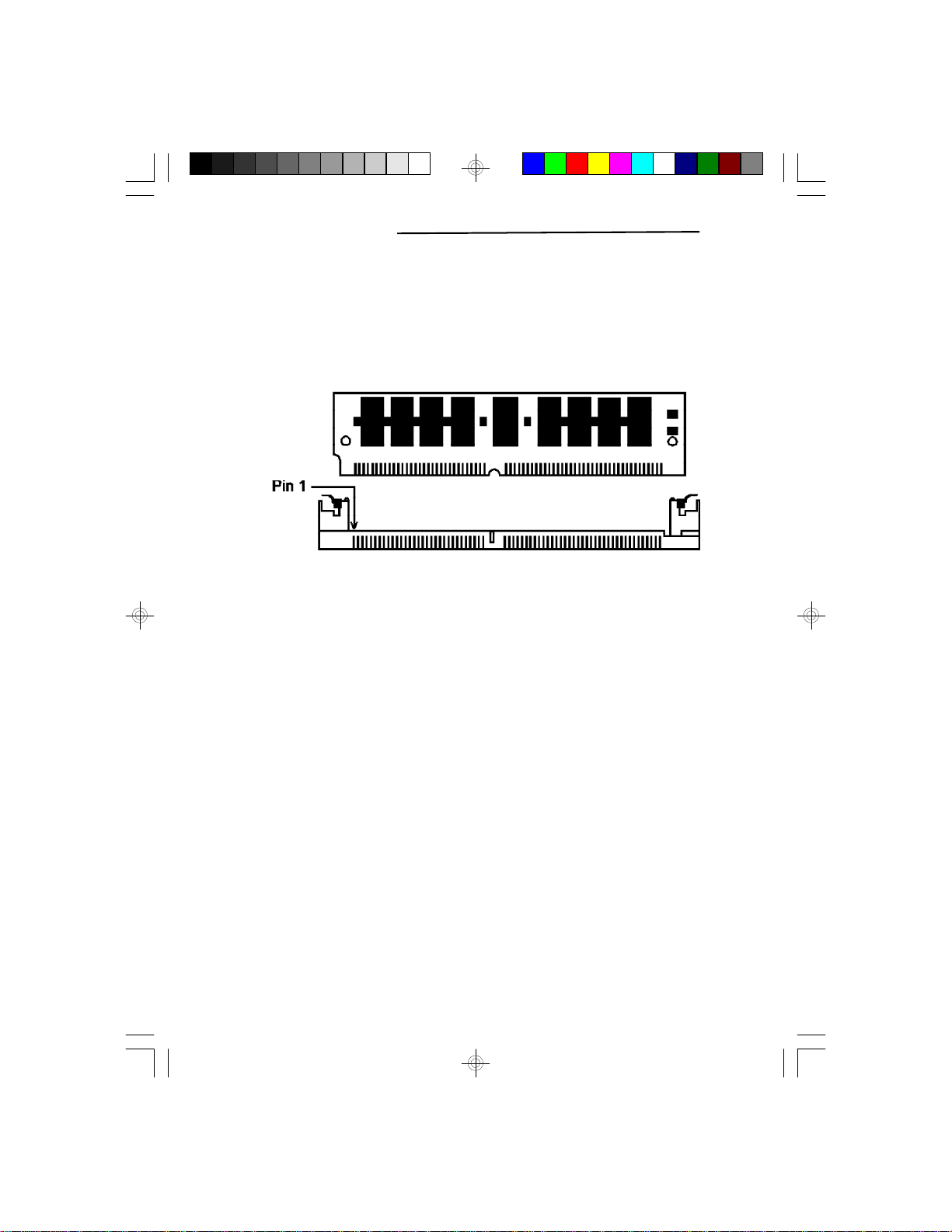
Installing the Modules
An HSIM module simply snaps into a socket on the
system board. Pin 1 of the HSIM module must correspond with Pin 1 of the socket.
1. Position the HSIM module above the socket with the
“notch” in the module aligned with the “key” on the
socket.
2. Seat the module at a 45o angle into the bank. Make
sure it is completely seated. Tilt the module upright
until it locks in place in the socket.
2-6 u Installation Overview
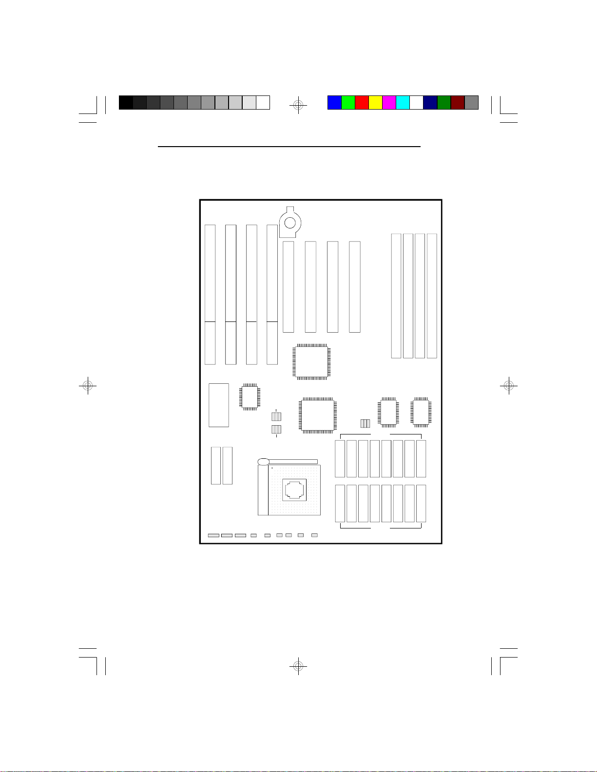
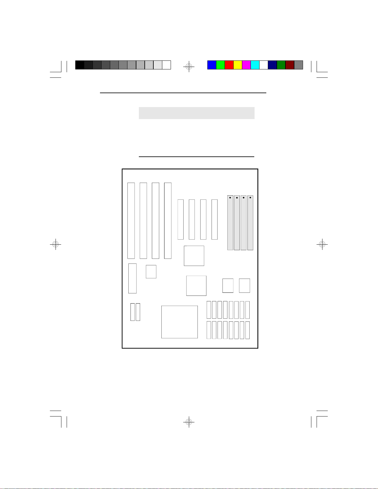
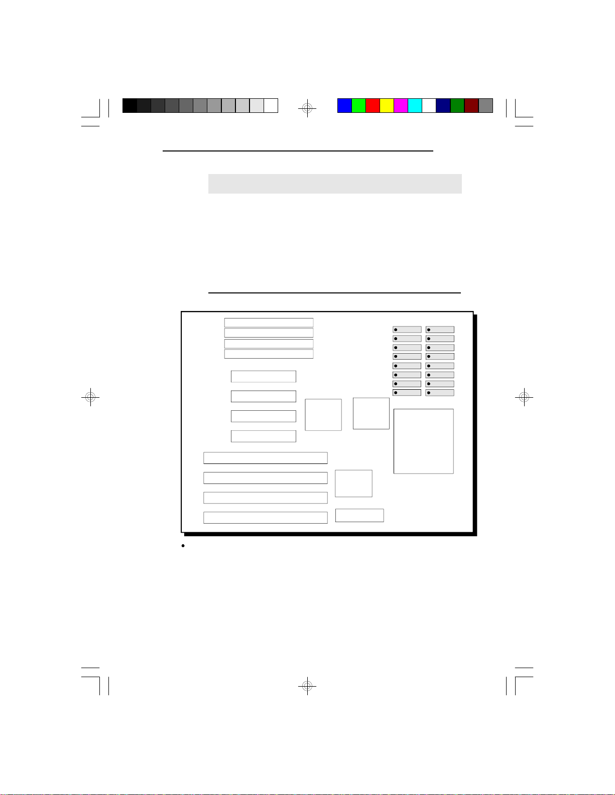
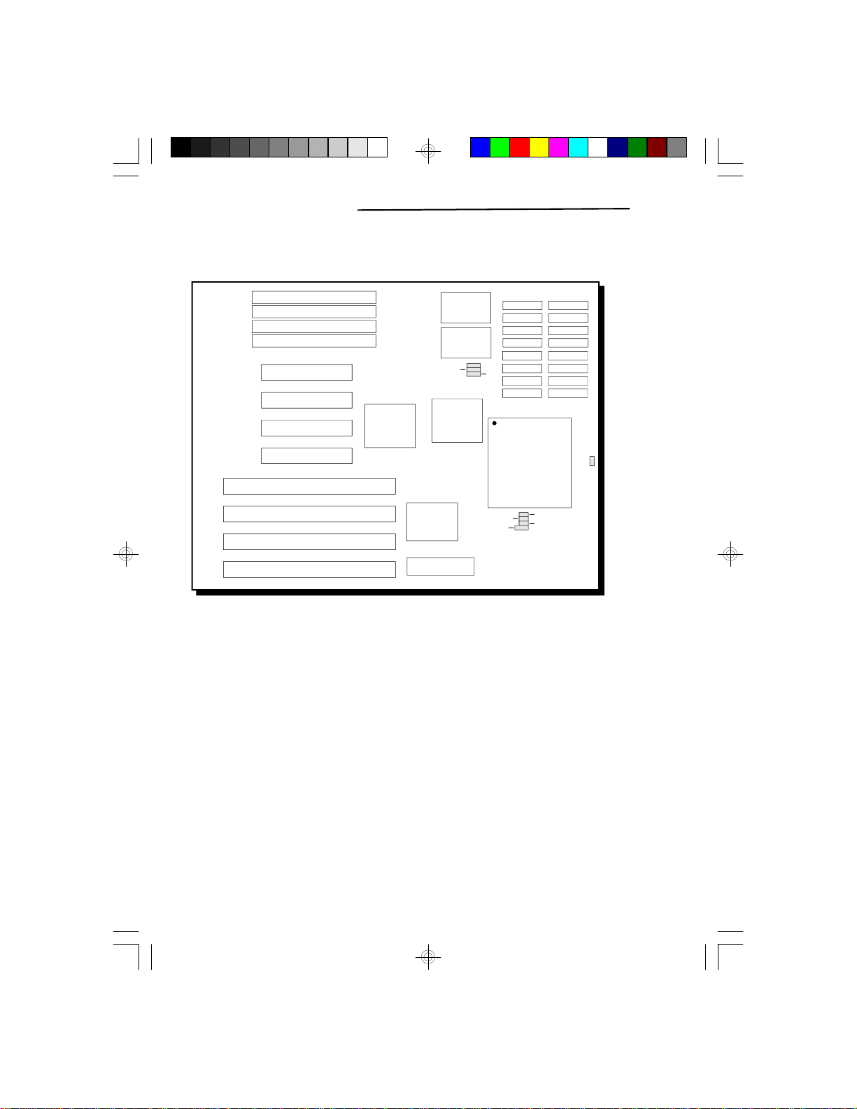
Board Configuration
ISA Slot
ISA Slot
ISA Slot
ISA Slot
VT82C416
VIA
System
BIOS
TAG
TAG
J8
J9 J7
J16
PCI 1
J15J17
PCI 2
VIA
VT82C576MV
VIA
VT82C575MV
G586VPB
PCI 3
PCI 4
J11
J10J12
Bank 1
SIM 4
VT82C577MV
VIA
SIM 3
SIM 2
SIM 1
VT82C577MV
VIA
CN15
CN13CN14
CN16CN17 J23
J22 CN12 CN11
Bank 0
Locations of Jumpers and Connectors
on the G586VPB System Board
Installation Overview u 2-7
Green PCI/ISA System Board
Jumper Settings
Jumper Settings for Internal Battery/CMOS Clean Select
SIM1
SIM2
SIM3
SIM4
PCI 4
PCI 3
PCI 2
PCI 1
J1
J2
ISA
ISA
ISA
ISA
Locations of Jumpers J1 and J2 on the G586VPB
System Board
2-8 u Installation Overview
G586VPB
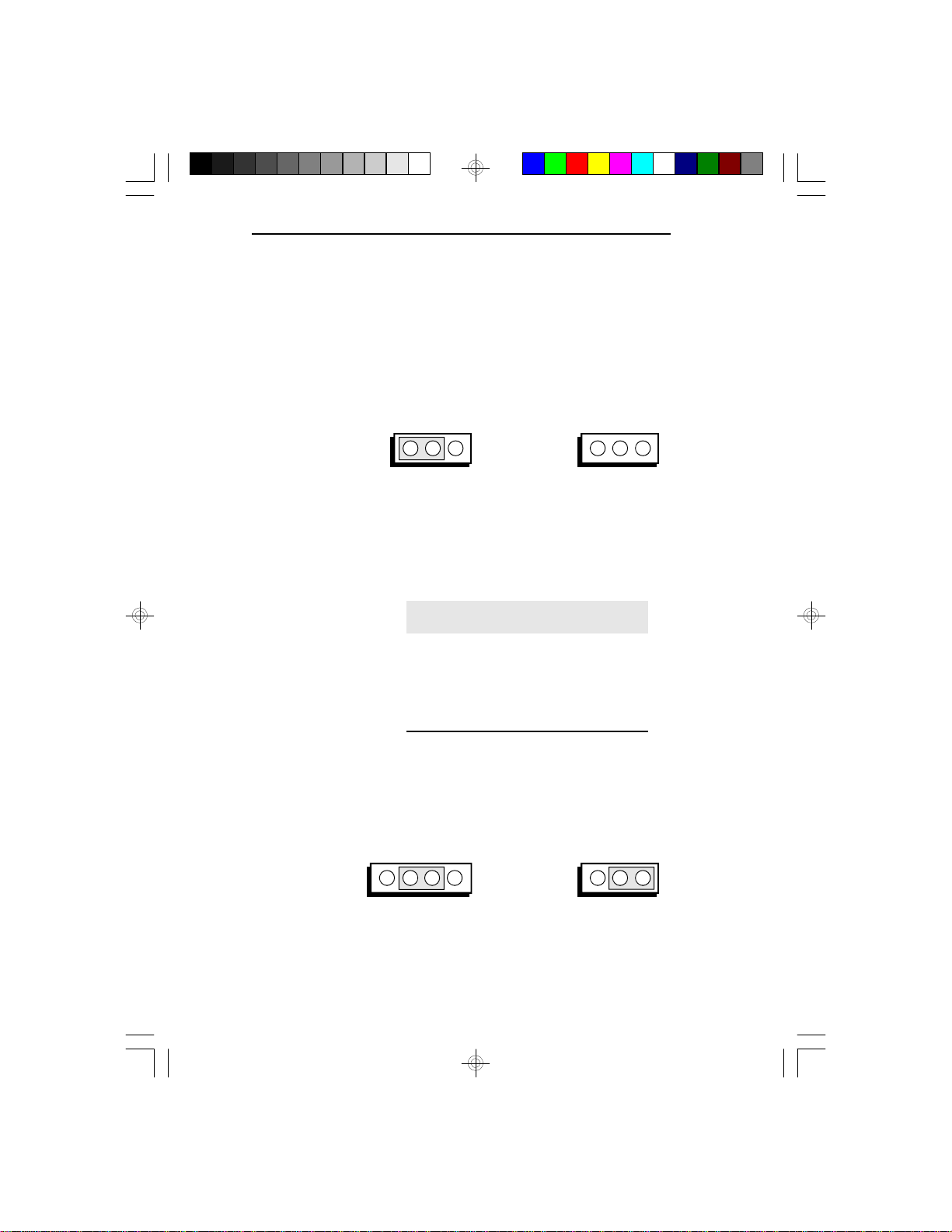
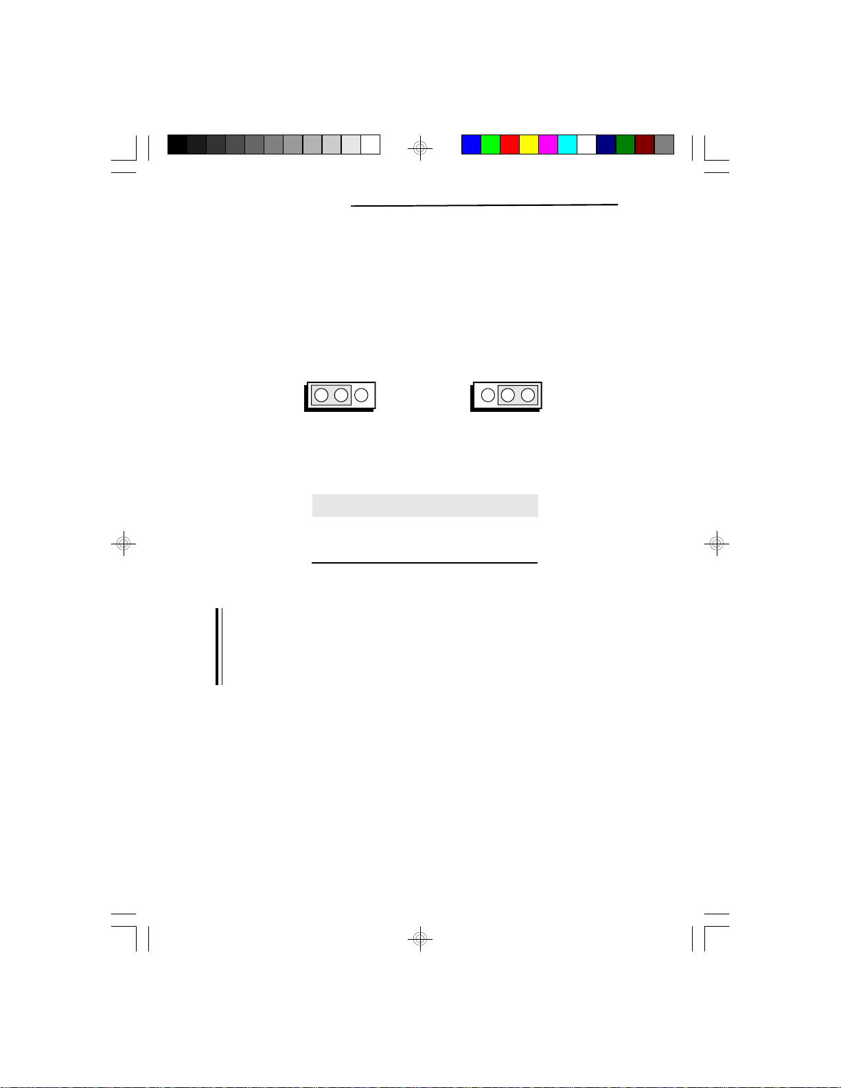
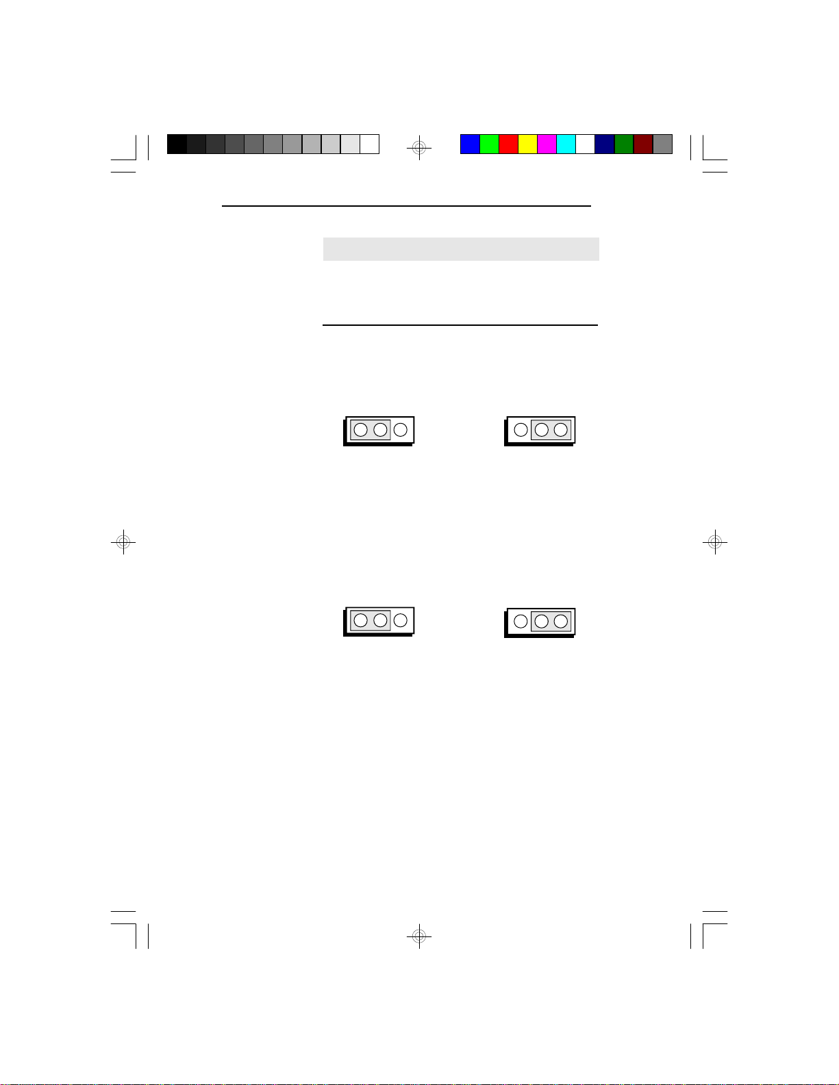
Jumpers/Connectors J1 and J2
Internal Battery/CMOS Clean Select
The G586VPB comes with an internal battery. If you
experience difficulty with the internal battery, or you
prefer to connect an external battery, set Jumper J2 to
Off and connect an external battery to Connector J1.
321
J2 : Internal Battery
Enabled (Default)
J2 Off: External
Battery Enabled
321
Connector J1
External Battery Connector
Pin
1
2
3
4
Function
Ext. Bat. Input
N. C.
GND
GND
If the CMOS becomes corrupted, the system can be
configured with the default values stored in the ROM
chips. To load the default values, change the setting of
Jumper J2 to pins 2-3 On. Set Jumper J1 pins 2-3 to On.
321
4
321
J1 pins 2-3 On: CMOS
Clean
Installation Overview u 2-9
J2 pins 2-3 On: CMOS
Clean

Green PCI/ISA System Board
Note:
After the CMOS has been reset, you must set Jumper J2
to Internal or External Battery Enable. If you set the
jumper to External Battery Enable, make sure you
connect an external battery to Connector J1.
Summary:
Caution:
The G586VPB system board uses 3V Lithium internal
battery. Battery may explode if mistreated. Do not
recharge, disassemble or dispose of in fire.
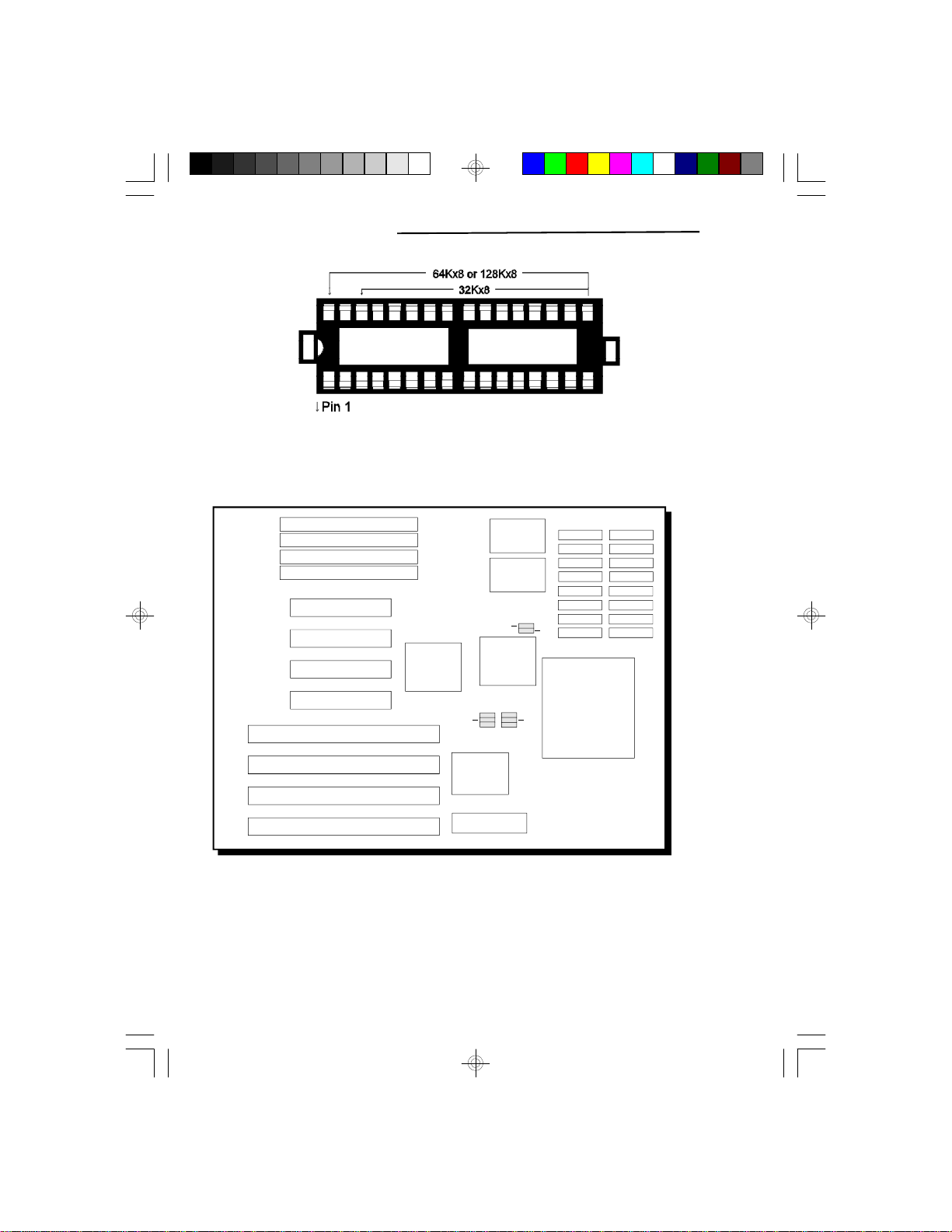
Cache Configuration
The G586VPB system board can be configured to four
different cache sizes: 256KB (Default size), 512KB,
1MB and 2MB. Either 32Kx8, 64Kx8 or 128Kx8 SRAM
chips are used for cache depending on the size of cache
desired. The G586VPB supports both pure 3.3V and
3.3/5V mixed voltage SRAM. The brands of SRAM that
passed a factory testing are shown on the next page.
J1
Internal Battery
External Battery
CMOS Clean
* External battery must be connected to Connector J1.
Off
On *
2-3 On
J2
1-2 On
Off
2-3 On
2-10 u Installation Overview
G586VPB
Brand/Model
Winbond:
W24M257AK-15
UMC:
UM61M256K-15
ISSI:
IS61LV256-15
Alliance:
ASTC3256-15
Cache Size
(32Kx8)
(32Kx8)
(32Kx8)
(32Kx8)
VT
82C576MV
Type of SRAM
Mixed voltage SRAM
Mixed voltage SRAM
Pure 3.3V SRAM
Pure 3.3V SRAM
Bank 1
U18
U19
U20
U21
U22
U23
U24
U25
VT
82C575MV
Socket
Bank 0
U33
U34
U35
U36
U37
U38
U39
U40
ZIF
Pin 1 of the SRAM socket
Locations of SRAM sockets on the G586VPB
System Board
Installation Overview u 2-11
Green PCI/ISA System Board
SRAM Socket
Jumper Settings for Cache Memory
J14
J16
Bank 1 Bank 0
ZIF
Socket
VT
82C576MV
82C577MV
82C577MV
82C575MV
J7
J8
J9
VT
82C416MV
VT
VT
J13
VT
J15
J17
Locations of Jumpers J7-J9 and J13-J17 on the
G586VPB System Board
2-12 u Installation Overview

G586VPB
Jumpers J7-J9 and J15-J17
Cache Size Setting
These jumpers should be set according to the cache size
shown below.
Cache Size
Data SRAM
U33-U40
U18-U25
Tag SRAM
U30, U31
J7
J8
J9
J15
J16
J17
* Default setting
256KB *
Bank 0
32Kx8
None
32Kx8
2-3 On
1-2 On
1-2 On
1-2 On
1-2 On
1-2 On
512KB
Bank 0
64Kx8
None
32Kx8
1-2 On
2-3 On
1-2 On
1-2 On
1-2 On
2-3 On
512KB
Bank 0/1
32Kx8
32Kx8
32Kx8
1-2 On
1-2 On
1-2 On
1-2 On
1-2 On
2-3 On
1MB
Bank 0
128Kx8
None
32Kx8
1-2 On
1-2 On
2-3 On
1-2 On
2-3 On
2-3 On
1MB
Bank 0/1
64Kx8
64Kx8
32Kx8
1-2 On
1-2 On
1-2 On
1-2 On
2-3 On
2-3 On
Warning:
Please note that you need to populate Bank 0 first and
then Bank 1. Failure to do so will cause the system
board to work improperly.
2MB
Bank 0/1
128Kx8
128Kx8
128Kx8
1-2 On
1-2 On
1-2 On
2-3 On
2-3 On
2-3 On
Installation Overview u 2-13
Green PCI/ISA System Board
Jumpers J13 and J14
SRAM Type Selection
The G586VPB can support two types of SRAM, 3.3V
SRAM and 3.3/5V mixed voltage SRAM. Settings for
Jumpers J13 and J14 should match the voltage of the
SRAM on the system board.
321 321
J13, J14 pins 1-2 On:
3.3/5V Mixed SRAM
J13, J14 pins 2-3 On:
Pure 3.3V SRAM
(Default)
J14
2-3 On
1-2 On
3.3V SRAM
3.3/5V SRAM *
* Default setting
J13
2-3 On
1-2 On
Note:
We recommend that you do not change the settings of
these jumpers because the settings have already been
determined according to the voltage of the SRAM chips
before their installation on the system board.
2-14 u Installation Overview
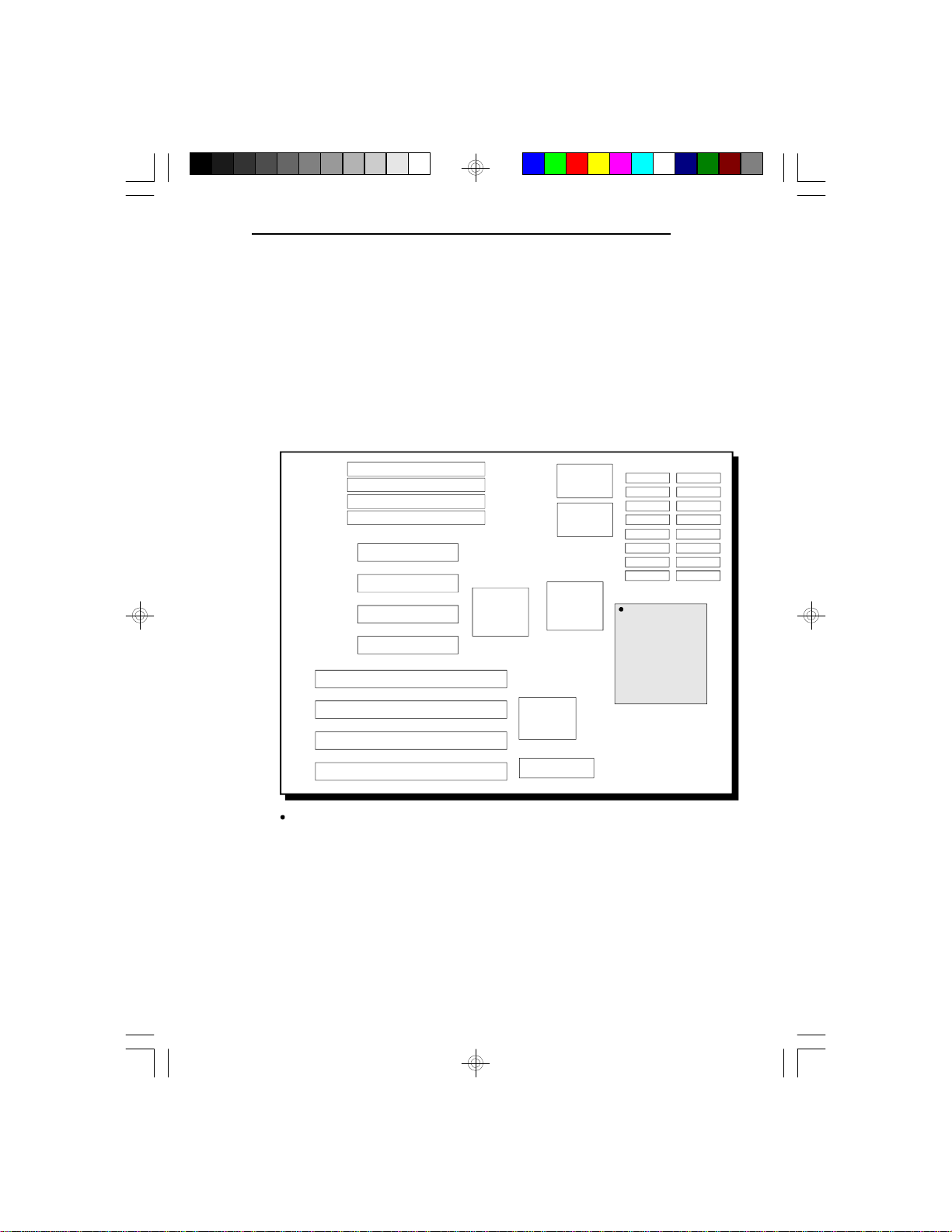
CPU Installation
The G586VPB is equipped with a 320-pin Zero Insertion
Force (ZIF) socket at location U32 of the system board.
The ZIF socket allows for easy installation of upgrade
CPUs as your system needs grow. Make sure all jumpers
are set correctly before applying power, or you may
damage the CPU or system board.
G586VPB
SIM1
SIM2
SIM3
SIM4
PCI 4
PCI 3
Pin 1 of the ZIF socket
PCI 2
PCI 1
ISA
ISA
ISA
ISA
VT
82C576MV
82C575MV
VT
82C416MV
System BIOS
Location of the ZIF Socket on the G586VPB
System Board
VT
82C577MV
VT
82C577MV
VT
U32
ZIF
Socket
Installation Overview u 2-15
Green PCI/ISA System Board
Jumper Settings for CPU
VT
82C577MV
J11
VT
82C575MV
J10
J12
ZIF
Socket
J22
VT
82C416MV
System BIOS
J18
J20
J19
J21
Locations of Jumpers J10-J12, J18, J19-J21 and J22 on the
G586VPB System Board
Jumpers J10, J11 and J12
System Base Clock Setting
The G586VPB supports System Base Clock external
frequency of 50MHz, 60MHz or 66MHz. Set the jumpers
J10-J12 according to the type of CPU installed in the
CPU socket.
2-16 u Installation Overview
G586VPB
50MHz
60MHz
66MHz *
* Default setting
J10
2-3 On
1-2 On
1-2 On
J11
1-2 On
1-2 On
2-3 On
J12
2-3 On
1-2 On
2-3 On
Default settings:
321 321
J10: 66MHz J11, J12: 66MHz
Jumper J18
CPU Write Back/Through Mode Control
Jumper J18 is used to select write back or write through
mode for CPU. Normally the write back mode is selected.
321 321
Pins 1-2 On: Write Back
Mode (Default)
Pins 2-3 On:Write
Through Mode
Jumpers J19, J20 and J21
CPU Power Setting
The G586VPB supports 3.3V, 3.45V and 3.8V CPUs.
Set jumpers J19, J20 and J21 according to the voltage
of the CPU installed on your system board.
Installation Overview u 2-17

Green PCI/ISA System Board
Default Settings:
J20
Off
On
Off
J21 Off: 3.3V
J21
Off
Off
On
J20 Off: 3.3VJ19 On: 3.3V
Voltage
3.3V *
3.45V
3.8V
* Default setting
J19
On
Off
Off
Jumper J22
CPU Mode Setting
Jumper J22 is used to select CPU internal frequency. You
should not change the default setting of this jumper unless
the CPU installed on the system board is 3.3V Pentium
Processor, System Base Clock frequency 50MHz.
Off:Fx1.5 (50MHz/
75MHz, 60MHz/90MHz
On: Fx2
(50MHz/100MHz)
or 66MHz/100Mhz CPU)
(Default)
2-18 u Installation Overview
 Loading...