

Page 1
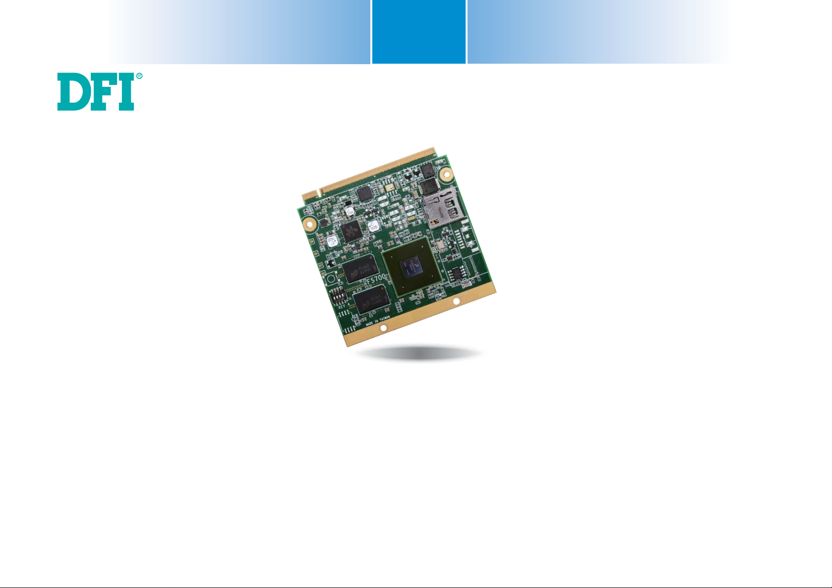
FS700 Series
Qseven Board
User’s Manual
A28540519
1
www.dfi .comChapter 1 Introduction
Page 2

Copyright
FCC and DOC Statement on Class B
This publication contains information that is protected by copyright. No part of it may be reproduced in any form or by any means or used to make any transformation/adaptation without
the prior written permission from the copyright holders.
This publication is provided for informational purposes only. The manufacturer makes no
representations or warranties with respect to the contents or use of this manual and specifically disclaims any express or implied warranties of merchantability or fitness for any particular
purpose. The user will assume the entire risk of the use or the results of the use of this document. Further, the manufacturer reserves the right to revise this publication and make changes
to its contents at any time, without obligation to notify any person or entity of such revisions
or changes.
Changes after the publication’s first release will be based on the product’s revision. The website
will always provide the most updated information.
© 2015. All Rights Reserved.
Trademarks
Product names or trademarks appearing in this manual are for identification purpose only and
are the properties of the respective owners.
Qseven Specification Reference
http://www.qseven-standard.org/
This equipment has been tested and found to comply with the limits for a Class B digital
device, pursuant to Part 15 of the FCC rules. These limits are designed to provide reasonable protection against harmful interference when the equipment is operated in a residential
installation. This equipment generates, uses and can radiate radio frequency energy and, if not
installed and used in accordance with the instruction manual, may cause harmful interference
to radio communications. However, there is no guarantee that interference will not occur in a
particular installation. If this equipment does cause harmful interference to radio or television
reception, which can be determined by turning the equipment off and on, the user is encouraged to try to correct the interference by one or more of the following measures:
• Reorient or relocate the receiving antenna.
• Increase the separation between the equipment and the receiver.
• Connect the equipment into an outlet on a circuit different from that to which the receiver
is connected.
• Consult the dealer or an experienced radio TV technician for help.
Notice:
1. The changes or modifications not expressly approved by the party responsible for compliance could void the user’s authority to operate the equipment.
2. Shielded interface cables must be used in order to comply with the emission limits.
2
www.dfi .comChapter 1 Introduction
Page 3

Table of Contents
Copyright .............................................................................................................2
Trademarks ........................................................................................................2
FCC and DOC Statement on Class B .....................................................2
About this Manual ..........................................................................................4
Warranty ............................................................................................................4
Static Electricity Precautions ......................................................................4
Safety Measures ..............................................................................................4
About the Package .........................................................................................5
Chapter 1 - Introduction .............................................................................6
Specifications ................................................................................................6
Features ..........................................................................................................7
Chapter 2 - Hardware Installation ................................................ 8
Board Layout .................................................................................................8
Block Diagram ...............................................................................................8
Mechanical Diagram ....................................................................................9
System Memory ............................................................................................9
MXM Connector ..........................................................................................10
MXM Connector Signal Description .......................................................12
Installing FS700 Series onto a Carrier Board ....................................17
3
www.dfi .comChapter 1 Introduction
Page 4
About this Manual
Static Electricity Precautions
An electronic file of this manual is included in the CD. To view the user’s manual in the CD, insert the CD into a CD-ROM drive. The autorun screen (Main Board Utility CD) will appear. Click
“User’s Manual” on the main menu.
Warranty
1. Warranty does not cover damages or failures that arised from misuse of the product, inability to use the product, unauthorized replacement or alteration of components and product specifications.
2. The warranty is void if the product has been subjected to physical abuse, improper installation, modification, accidents or unauthorized repair of the product.
3. Unless otherwise instructed in this user’s manual, the user may not, under any circumstances, attempt to perform service, adjustments or repairs on the product, whether in or
out of warranty. It must be returned to the purchase point, factory or authorized service
agency for all such work.
4. We will not be liable for any indirect, special, incidental or consequencial damages to the
product that has been modified or altered.
It is quite easy to inadvertently damage your PC, system board, components or devices even
before installing them in your system unit. Static electrical discharge can damage computer
components without causing any signs of physical damage. You must take extra care in handling them to ensure against electrostatic build-up.
1. To prevent electrostatic build-up, leave the system board in its anti-static bag until you are
ready to install it.
2. Wear an antistatic wrist strap.
3. Do all preparation work on a static-free surface.
4. Hold the device only by its edges. Be careful not to touch any of the components, contacts
or connections.
5. Avoid touching the pins or contacts on all modules and connectors. Hold modules or connectors by their ends.
Important:
Electrostatic discharge (ESD) can damage your processor, disk drive and other components. Perform the upgrade instruction procedures described at an ESD workstation only. If such a station is not available, you can provide some ESD protection by
wearing an antistatic wrist strap and attaching it to a metal part of the system chassis. If a wrist strap is unavailable, establish and maintain contact with the system
chassis throughout any procedures requiring ESD protection.
Safety Measures
To avoid damage to the system:
• Use the correct AC input voltage range.
To reduce the risk of electric shock:
• Unplug the power cord before removing the system chassis cover for installation or servicing. After installation or servicing, cover the system chassis before plugging the power
cord.
4
www.dfi .comChapter 1 Introduction
Page 5

About the Package
The package contains the following items. If any of these items are missing or damaged,
please contact your dealer or sales representative for assistance.
• One FS700-M60 board
• One Heat spreader (for temperature -40°C to 85°C only)
• One QR (Quick Reference)
Optional Items
• Q7A-551 carrier board kit
• WM-240 WiFi kit
• UC20 Mini-PCIe UMTS/HSPA+ Module
The board and accessories in the package may not come similar to the information listed
above. This may differ in accordance with the sales region or models in which it was sold. For
more information about the standard package in your region, please contact your dealer or
sales representative.
5
www.dfi .comChapter 1 Introduction
Page 6
Chapter 1 - Introduction
Specifications
Chapter 1
Processor
System Memory
Graphics
Audio
LAN
Serial ATA
eMMC
microSD
Expansion
Interfaces
OS Support
Watchdog
Timer
Power
• Freescale i.MX 6 series processors
- i.MX6Q: i.MX 6Quad, up to 1.0GHz, Four Cortex-A9 cores
- i.MX6D: i.MX 6Dual, up to 1.0GHz, Two Cortex-A9 cores
- i.MX6L: i.MX 6DualLite, up to 1.0GHz, Two Cortex-A9 cores
- i.MX6S: i.MX 6Solo, up to 1.0GHz, One Cortex-A9 core
• 1GB/2GB DDR3 memory down
• Supports HDMI and LVDS interfaces
• HDMI: HDMI v1.4 resolution up to 1920x1200 @60Hz
• LVDS: 18/24-bit
- One port up to 165 Mpixels/sec (e.g. 2560x1600 @ 60Hz)
- Two ports up to 85 Mpixels/sec (e.g. WUXGA+ @ 60Hz) each
• Built-in Video, 2D graphics and 3D graphics processors
• Supports OpenCL, OpenVG 1.1 and 1080p/720p decoder/encoder
• Supports I2S interface
• One Atheros AR8033 Ethernet PHY
• Supports 10Mbps, 100Mbps and 1Gbps data transmission
• Supports 1 SATA 2.0 interface (Quad and Dual processors only)
• SATA speed up to 3Gb/s (SATA 2.0)
• Supports 4GB (standard), 8GB and 16GB eMMC onboard
• 1 microSD socket
• Supports 4 USB 2.0 interfaces
• Supports 1 USB OTG (Type B) interface
• Supports 1 PCIe x1 interface
• Supports 1 RS232 serial interface
• Supports 2 I
• Supports CAN-bus (Controller-Area Network) interface
• Supports SDIO interface
• LTIB Linux 3.0.35
• Android 4.3
- Quad, Dual and DualLite processors only
• Software programmable
• Input: 5V
2
C interface
(Default Preloaded)
Power
Consumption
Temperature
Humidity
PCB
• Under 5W @ 5V
• Operating
o
C to 60oC - DualLite, Solo
: 0
o
: -40
C to 85oC - Quad, Dual
• Storage: -40
• 5% to 90%
• Dimensions
- Qseven form factor
- 70mm (2.76") x 70mm (2.76")
• Compliance
- Qseven specifi cation revision 1.2
o
C to 85oC
6
www.dfi .comChapter 1 Introduction
Page 7

Chapter 1
A
g
p
)
p
play
,
A
/Gig
t
p
t
y
g
r
p
)
y
Features
• DDR3
DDR3 delivers increased system bandwidth and improved performance. The advantages of
DDR3 are its higher bandwidth and its increase in performance at a lower power than DDR2.
• Graphics
The integrated Intel® HD graphics engine delivers an excellent blend of graphics performance
and features to meet business needs. It provides excellent video and 3D graphics with outstanding graphics responsiveness. These enhancements deliver the performance and compatibility needed for today’s and tomorrow’s business applications. Supports HDMI and LVDS
display outputs.
• Serial ATA
Serial ATA is a storage interface that is compliant with SATA 2.0a specification. With speed of
up to 3Gb/s (SATA 2.0), it improves hard drive performance faster than the standard parallel
ATA whose data transfer rate is 100MB/s. The bandwidth of the SATA 3.0 will be limited by
carrier board design.
• Gigabit LAN
The Atheros AR8033 Ethernet Phy controller supports up to 1Gbps data transmission.
Important:
The DFI FS700 Series Qseven module provides Gigabit Ethernet with one Atheros
AR8033 Ethernet PHY. The maximum throughput that the Gigabit Ethernet performs is
limited to 470Mbps (total for Tx and Rx) due to internal bus limitations based on Freescale’s Errata ERR004512. The actual measurement of the Gigabit Ethernet controller
used on the FS700 Series system board is up to 380Mbps. This difference might be
caused by the software configuration, network environment or equipment.
Specification Comparison Table
The table below shows the Qseven standard specifications and the corresponding specifications
supported on the FS700 module.
System I/O Interface
PCI Ex
ress Lanes 0 1 (x1 link
Serial ATA channels 0 0 2 1
USB 2.0
orts 3 4 8 5
LVDS channels 0 0 Dual Channel 24bits 2
Port, TMDS
Dis
High Definition
udio/AC'97
Ethernet 10/100
Mbit
abi
ressCard support0020
Ex
Low Pin Count bus 0 0 1 0
Secure Digital I/O 8-bi
for SD/MMC cards
S
stem Management 0 1 1 0
2
C Bus
I
SPI Bus 0 0 1 1
CAN Bus 0 0 1 1
Trigge
Watchdo
Power Button 1 1 1 1
Power Good 1 1 1 1
Reset Button 1 1 1 1
LID Button 0 0 1 1
Slee
Button 0 0 1 1
Suspend To RAM (S3
mode
Wake 0 0 1 1
Batter
low alarm 0 0 1 1
Thermal control 0 0 1 0
FAN control 0 0 1 0
RM/RISC Based
Minimum Confi
0011
001
0 0 1 (Gigabit Ethernet) 1
0011
1112
1110
0011
uration
X86 Based Minimum
Configuration
Maximum
Configuration
41
DFI FS700 Series
Configuration
2
S
I
• USB
The system board supports USB 2.0 and USB 1.1 ports. USB 1.1 supports 12Mb/second bandwidth while USB 2.0 supports 480Mb/second bandwidth providing a marked improvement in
device transfer speeds between your computer and a wide range of simultaneously accessible
external Plug and Play peripherals.
• Watchdog Timer
The Watchdog Timer function allows your application to regularly “clear” the system at the set
time interval. If the system hangs or fails to function, it will reset at the set time interval so
that your system will continue to operate.
7
www.dfi .comChapter 1 Introduction
Page 8

Chapter 2 - Hardware Installation
24 bits LVDS
Backlight
C 2
HDMI
24 bits LVDS
USB OTG
SDIO (SD3)
SATA
CAN Bus
PCIe
SPI 1
UART5
Power
ON
Reset
Power
Board Layout
Chapter 2
Block Diagram
24 bits LVDS
Boot Device Select
234
(Switch)
1
ON
DDR3 DDR3
Freescale
i.MX6 Series
microSD
eMMC
PMIC
MMPF0100
USB HUB
USB2514BI
Top View
24 bits LVDS
Backlight
2
C 2
I
HDMI
RGMIIMDI
GLAN PHY
AMXM Golden Finger
UART5
SATA
PCIe
SPI 1
CAN Bus
SDIO (SD3)
HDA (I2S)
Freescale
i.MX6
SD4
SD2
I2C
MIPI CSI
UART1
DDR3
eMMC
micro SD
Sensor
Camera
Power ON
Reset
Bottom View
USB OTG
DDR3DDR3
Atheros
AR8033
USB 0-3 USB
Power
USB Hub
Power
PMIC
8
www.dfi .comChapter 2 Hardware Installation
Page 9

Chapter 2
Mechanical Diagram
FS700 Series Module
23.65
0.00
3.00
18.00
38.92
52.00
67.00
70.00
0.00
2.50
56.50
64.90
70.00
3.95
11.53
Top View
66.06
Important:
Electrostatic discharge (ESD) can damage your processor, disk drive and other components. Perform the upgrade instruction procedures described at an ESD workstation only. If such a station is not available, you can provide some ESD protection by
wearing an antistatic wrist strap and attaching it to a metal part of the system chassis. If a wrist strap is unavailable, establish and maintain contact with the system
chassis throughout any procedures requiring ESD protection.
System Memory
The system board is equipped two 1GB onboard system memorys that support DDR3.
DDR3
DDR3
Bottom View
9
www.dfi .comChapter 2 Hardware Installation
Page 10

Chapter 2
MXM Connector
MXM Connector
The MXM connector is used to interface with the carrier board. Insert FS700 series to the MXM
connector on the carrier board. Refer to the following pages for the pin functions of this connector.
Refer to “Installing FS700 Series onto a Carrier Board” section for more information.
Pin Signal Pin Signal
1GND 2GND
3 GBE_MDI3- 4 GBE_MDI25 GBE_MDI3+ 6 GBE_MDI2+
7 GBE_LINK100# 8 GBE_LINK1000#
9 GBE_MDI1- 10 GBE_MDI011 GBE_MDI1+ 12 GBE_MDI0+
13 GBE_LINK# 14 GBE_ACT#
15 16 SUS_S5#
17 WAKE# 18 SUS_S3#
19 SUS_STAT# 20 PWRBTN#
21 SLP_BTN# 22 LID_BTN#
23 GND 24 GND
25 GND 26 PWGIN
27 BATLOW# 28 RSTBTN#
29 SATA0_TX+ 30
31 SATA0_TX- 32
33 SATA0_ACT# 34 GND
35 SATA0_RX+ 36
37 SATA0_RX- 38
39 GND 40 GND
41 BIOS_DISABLE#/BOOT_ALT# 42 SDIO_CLK
43 SDIO_CD# 44 SDIO_LED
45 SDIO_CMD 46 SDIO_WP
47 SDIO_PWR# 48 SDIO_DAT1
49 SDIO_DAT0 50 SDIO_DAT3
51 SDIO_DAT2 52 SDIO_DAT5
53 SDIO_DAT4 54 SDIO_DAT7
55 SDIO_DAT6 56 RSVD
57 GND 58 GND
59 I2S_TXFS 60 SMB_CLK
61 I2S_CLK 62 SMB_DAT
63 I2S_TXC 64 SMB_ALERT#
65 I2S_RXD 66 I2C_CLK
67 I2S_TXD 68 I2C_DAT
69 70 WDTRIG#
71 72 WDOUT
73 GND 74 GND
75 76
77 78
79 80 USB_4_5_OC#
81 82 USB_P483 84 USB_P4+
85 USB_2_3_OC# 86 USB_0_1_OC#
87 USB_P3- 88 USB_P289 USB_P3+ 90 USB_P2+
91 USB_CC 92 USB_ID
93 USB_P1- 94 USB_P095 USB_P1+ 96 USB_P0+
97 GND 98 GND
99 LVDS_A0+ 100 LVDS_B0+
10
www.dfi .comChapter 2 Hardware Installation
Page 11

Chapter 2
Pin Signal Pin Signal
101 LVDS_A0- 102 LVDS_B0103 LVDS_A1+ 104 LVDS_B1+
105 LVDS_A1- 106 LVDS_B1107 LVDS_A2+ 108 LVDS_B2+
109 LVDS_A2- 110 LVDS_B2-
LVDS_PPEN
111
LVDS_A3+
113
LVDS_A3-
115
GND
117
LVDS_A_CLK+
119
LVDS_A_CLK-
121
LVDS_BLT_CTRL/GP_PWM_OUT0
123
LVDS_DID_DAT/GP_I2C_DAT
125
LVDS_DID_CLK/GP_I2C_CLK
127
CAN0_TX
129
TMDS_CLK+
131
TMDS_CLK-
133
GND
135
TMDS_LANE1+
137
TMDS_LANE1-
139
GND
141
TMDS_LANE0+
143
TMDS_LANE0-
145
GND
147
TMDS_LANE2+
149
TMDS_LANE2-
151
HDMI_HPD#
153
PCIE_CLK_REF+
155
PCIE_CLK_REF-
157
GND
159
161 162
163 164
GND
165
167 168
169 170
UART_TXD
171
173 174
175 176
UART_RXD
177
PCIE0_TX+
179
PCIE0_TX-
181
GND
183
185 186
187 188
189 190
191 192
VCC_RTC
193
195 196
GND
197
SPI_MOS1
199
LVDS_BLEN
112
114 LVDS_B3+
116 LVDS_B3-
GND
118
LVDS_B_CLK+
120
LVDS_B_CLK-
122
RSVD
124
LVDS_BLC_DAT
126
LVDS_BLC_CLK
128
CAN0_RX
130
132
134
GND
136
138
140
GND
142
144
146
GND
148
HDMI_CTRL_DAT
150
HDMI_CTRL_CLK
152
154
PCIE_WAKE#
156
PCIE_RST#
158
GND
160
GND
166
UART_RTS
172
UART_CTS
178
PCIE0_RX+
180
PCIE0_RX-
182
GND
184
194
GND
198
SPI_CS0#
200
Pin Signal Pin Signal
SPI_MOS0
201
203
205
207
209
211
213
215
217
219
221
223
225
227
229
SPI_SCK
5V_SB
MFG_NC0
MFG_NC1
VCC (+5V)
VCC (+5V)
VCC (+5V)
VCC (+5V)
VCC (+5V)
VCC (+5V)
VCC (+5V)
VCC (+5V)
VCC (+5V)
VCC (+5V)
202
204
206
208
210
212
214
216
218
220
222
224
226
228
230
MFG_NC4
5V_SB
MFG_NC2
MFG_NC3
VCC (+5V)
VCC (+5V)
VCC (+5V)
VCC (+5V)
VCC (+5V)
VCC (+5V)
VCC (+5V)
VCC (+5V)
VCC (+5V)
VCC (+5V)
11
www.dfi .comChapter 2 Hardware Installation
Page 12

Chapter 2
-
+
-
+
-
+
A
e
A
e
A
e
A
e
MXM Connector Signal Description
Pin Types
I Input Pin
O Output Pin
I/O Bi-directional input / output Pin
OD Open drain
PP Push Pull
NC Not Connected
PCI Express Interface Signals Descriptions
Signal Pin# Pin Type Pwr Rail /Tolerance DFI-FS700 Series Carrier Board Description
PCIE0_RX+ 180
PCIE0_RX- 182
PCIE0_TX+
PCIE0_TXPCIE_CLK_REF+ 155
PCIE_CLK_REF- 157
PCIE_WAKE# 156 I CMOS 3.3V Suspend/3.3V PCI Express Wake Event: Sideband wake signal asserted by components requesting wakeup.
PCIE_RST# 158 O CMOS 3.3V/3.3V Reset Signal for external devices.
Express Card Support Pins
Signal Pin# Pin Type Pwr Rail /Tolerance DFI-FS700 Series Carrier Board Description
UART_RXD 177 I CMOS 3.3V UART RXD
UART_TXD 171 O CMOS 3.3V UART TXD
UART_CTS 178 I CMOS 3.3V UART CTS
UART_RTS 172 O CMOS 3.3V UART RTS
Gigabit Ethernet Signals
Signal Pin# Pin Type Pwr Rail /Tolerance DFI-FS700 Series Carrier Board Description
GBE_MDI0+ 12
GBE_MDI0
GBE_MDI1
GBE_MDI1
GBE_MDI2
GBE_MDI2
GBE_MDI3
GBE_MDI3- 3
GBE_LINK# 13 OD CMOS 3.3V Suspend/3.3V NC Gigabit Ethernet Controller 0 link indicator, active low.
GBE_LINK100# 7 OD CMOS 3.3V Suspend/3.3V
GBE_LINK1000# 8 OD CMOS 3.3V Suspend/3.3V
GBE_ACT# 14 OD CMOS 3.3V Suspend/3.3V
Serial ATA Interface Signals
Signal Pin# Pin Type Pwr Rail /Tolerance DFI-FS700 Series Carrier Board Description
SATA0_RX+ 35
SATA0_RX- 37
SATA0_TX+ 29
SATA0_TX- 31
SATA_ACT# 33 I/O CMOS 3.3V/3.3V Serial ATA Led. Open collector output pin driven during SATA command activity.
I PCIE
179
O PCUE
181
O PCUE PCIE
I/O Analog
10
11
I/O Analog
9
6
I/O Analog
4
5
I/O Analog
I SATA
O SATA
AC coupled off Module
AC coupled on Module
3.3V max Suspend
3.3V max Suspend
3.3V max Suspend
3.3V max Suspend
C coupled on Modul
C coupled on Modul
C coupled on Modul
C coupled on Modul
AC Coupling capacitor
AC Coupling capacitor
Device - Connect AC Coupling cap 0.1uF
Slot - Connect to PCIE Conn pin
Connect to PCIE device or slot
Connect to PCIE device, PCIe CLK Buffer or slot
Connect to Magnetics Module MDI0+/-
Connect to Magnetics Module MDI1+/Connect to Magnetics Module MDI2+/-
Connect to Magnetics Module MDI3+/-
Connect to LED and recommend current limit resistor 150ȟ to
3.3VSB
Connect to LED and recommend current limit resistor 150ȟ to
3.3VSB
Connect to LED and recommend current limit resistor 150ȟ to
3.3VSB
Connect to SATA0 Conn RX pin
Connect to SATA0 Conn TX pin
PCI Express channel 0, Receive Input differential pair.
PCI Express channel 0, Transmit Output differential pair.
Reference clock output for all PCI Express and PCI Express Graphics
lanes.
Gigabit Ethernet Controller 0: Media Dependent Interface Differential
Pairs 0,1,2,3. The MDI can operate in 1000, 100 and 10 Mbit / sec
modes. Some pairs are unused in some modes, per the following:
1000BASE-T 100BASE-TX 10BASE-T
MDI[0]+/- B1_DA+/- TX+/- TX+/ MDI[1]+/- B1_DB+/- RX+/- RX+/ MDI[2]+/- B1_DC+/ MDI[3]+/- B1_DD+/-
Gigabit Ethernet Controller 0 1000 Mbit / sec link indicator, active low.
Gigabit Ethernet Controller 0 1000 Mbit / sec link indicator, active low.
Gigabit Ethernet Controller 0 activity indicator, active low.
Serial ATA or SAS Channel 0 receive differential pair.
Serial ATA or SAS Channel 0 transmit differential pair.
Important:
The DFI FS700 Series Qseven module provides Gigabit Ethernet with one Atheros
AR8033 Ethernet PHY. The maximum throughput that the Gigabit Ethernet performs is
limited to 470Mbps (total for Tx and Rx) due to internal bus limitations based on Freescale’s Errata ERR004512. The actual measurement of the Gigabit Ethernet controller
used on the FS700 Series system board is up to 380Mbps. This difference might be
caused by the software configuration, network environment or equipment.
12
www.dfi .comChapter 2 Hardware Installation
Page 13

Chapter 2
USB Interface Signals
Signal Pin# Pin Type Pwr Rail /Tolerance DFI-FS700 Series Carrier Board Description
USB_P0+ 96
USB_P0- 94
USB_P1+ 95
USB_P1- 93
USB_P2+ 90
USB_P2- 88
USB_P3+ 89
USB_P3- 87
USB_P4+ 84
USB_P4- 82
USB_0_1_OC# 86 I CMOS 3.3V Suspend/3.3V
USB_2_3_OC# 85 I CMOS 3.3V Suspend/3.3V
USB_4_5_OC# 80 I CMOS 3.3V Suspend/3.3V
USB_ID 92 I CMOS 3.3V Suspend/3.3V
USB_CC 91 I CMOS 3.3V Suspend/3.3V
SDIO Interface Signals
Signal Pin# Pin Type Pwr Rail /Tolerance DFI-FS700 Series Carrier Board Description
SDIO_CD# 43 I/O CMOS 3.3V/3.3V SDIO Card Detect. This signal indicates when a SDIO/MMC card is present.
SDIO_CLK 42 O CMOS 3.3V/3.3V SDIO Clock. With each cycle of this signal a one-bit transfer on the command and each data line occurs. This signal has maximum frequency of 48 MHz.
SDIO_CMD 45 I/O OD/PP CMOS 3.3V/3.3V
SDIO_LED 44 O CMOS 3.3V/3.3V SDIO LED. Used to drive an external LED to indicate when transfers occur on the bus.
SDIO_WP 46 I/O CMOS 3.3V/3.3V SDIO Write Protect. This signal denotes the state of the write-protect tab on SD cards.
SDIO_PWR# 47 O CMOS 3.3V/3.3V SDIO Power Enable. This signal is used to enable the power being supplied to a SD/MMC card device.
SDIO_DAT0-7 48-55 I/O PP CMOS 3.3V/3.3V SDIO Data lines. These signals operate in push-pull mode
High Definition Audio Signals/AC'97
Signal Pin# Pin Type Pwr Rail /Tolerance DFI-FS700 Series Carrier Board Description
I2S_CLK 61 O CMOS 3.3V/3.3V I2S Clock outout
I2S_TXFS 59 O CMOS 3.3V/3.3V I2S TXFS
I2C_TXC 63 O CMOS 3.3V/3.3V I2C TXC
I2S_TXD 67 O CMOS 3.3V/3.3V I2S TXD
I2S_RXD 65 I CMOS 3.3V/3.3V I2 RXD
I/O USB
I/O USB
I/O USB
I/O USB
3.3V Suspend/3.3V
3.3V Suspend/3.3V
3.3V Suspend/3.3V
3.3V Suspend/3.3V
3.3V Suspend/3.3V
PU 10k to 3.3VSB Connect to Overcurrent of USB Power Switch
PU 10k to 3.3VSB Connect to Overcurrent of USB Power Switch
PU 10k to 3.3VSB Connect to Overcurrent of USB Power Switch
Connect 90ಳ @100MHz Common Choke in series and ESD
suppressors to GND to USB connector
Connect 90ಳ @100MHz Common Choke in series and ESD
suppressors to GND to USB connector
Connect 90ಳ @100MHz Common Choke in series and ESD
suppressors to GND to USB connector
Connect 90ಳ @100MHz Common Choke in series and ESD
suppressors to GND to USB connector
Connect 90ಳ @100MHz Common Choke in series and ESD
suppressors to GND to USB connector
Universal Serial Bus Port 0 differential pair.I/O USB
Universal Serial Bus Port 1 differential pair.This port may be optionally used as USB client port.
Universal Serial Bus Port 2 differential pair.
Universal Serial Bus Port 3 differential pair.
Universal Serial Bus Port 4 differential pair.
USB over-current sense, USB channels 0 and 1. A pull-up for this line shall be present on the Module. An open drain driver from a USB current monitor on the Carrier Board may drive this line
low.
Do not pull this line high on the Carrier Board.
USB over-current sense, USB channels 0 and 1. A pull-up for this line shall be present on the Module. An open drain driver from a USB current monitor on the Carrier Board may drive this line
low.
Do not pull this line high on the Carrier Board.
USB over-current sense, USB channels 0 and 1.
A pull-up for this line shall be present on the Module. An open drain driver from a USB current monitor on the Carrier Board may drive this line low.
Do not pull this line high on the Carrier Board.
USB ID pin.Configures the mode of the USB Port 1. If the signal is detected as being 'high active' the BIOS will automatically configure USB Port 1 as USB Client and enable USB Client support.
This signal should be driven as OC signal by external circuitry.
USB Client Connect pin.If USB Port 1 is configured for client mode then an externally connected USB host should set this signal to high-active in order to properly make the connection with the
module's internal USB client controller.
If the external USB host is disconnected, this signal should be set to low-active in order to inform the USB client controller that the external host has been disconnected.
A level shifter/protection circuitry should be implemented on the carrier board for this signal.
SDIO Command/Response. This signal is used for card initialization and for command transfers. During initialization mode this signal is open drain. During command transfer this signal is in pushpull mode.
13
www.dfi .comChapter 2 Hardware Installation
Page 14

Chapter 2
e
.
LVDS Flat Panel Signals
Signal Pin# Pin Type Pwr Rail /Tolerance DFI-FS700 Series Carrier Board Description
LVDS_PPEN 111 O CMOS 3.3V/3.3V
LVDS_BLEN 112 O CMOS 3.3V/3.3V
LVDS_BLT_CTRL/GP_PWM_OUT0 123 O CMOS 3.3V/3.3V
LVDS_A0+ 99
LVDS_A0- 101
LVDS_A1+ 103
LVDS_A1- 105
LVDS_A2+ 107
LVDS_A2- 109
LVDS_A3+ 113
LVDS_A3- 115
LVDS_A_CLK+ 119
LVDS_A_CLK- 121
LVDS_B0+ 100
LVDS_B0- 102
LVDS_B1+ 104
LVDS_B1- 106
LVDS_B2+ 108
LVDS_B2- 110
LVDS_B3+ 114
LVDS_B3- 112
LVDS_B_CLK+ 120
LVDS_B_CLK- 122
LVDS_DID_CLK/GP_I2C_CLK 127 I/O OD CMOS 3.3V/3.3V
LVDS_DID_DAT/GP_I2C_DAT 125 I/O OD CMOS 3.3V/3.3V
LVDS_BLC_CLK 128 I/O OD CMOS 3.3V/3.3V
LVDS_BLC_DAT 126 I/O OD CMOS 3.3V/3.3V
HDMI Interface Signals
Signal Pin# Pin Type Pwr Rail /Tolerance DFI-FS700 Series Carrier Board Description
TMDS_CLK- 133
TMDS_CLK+ 131
TMDS_LANE0- 145
TMDS_LANE0+ 143
TMDS_LANE1- 139
TMDS_LANE1+ 137
TMDS_LANE2- 151
TMDS_LANE2+ 149
HDMI_CTRL_CLK (SDVO_CTRL_CLK) 152 I/O OD CMOS 3.3V/3.3V
HDMI_CTRL_DAT (SDVO_CTRL_DAT) 150 I/O OD CMOS 3.3V/3.3V
HDMI_HPD# 153 I CMOS 3.3V/3.3V
O LVDS
O LVDS
O LVDS
O LVDS
O LVDS
O LVDS
O LVDS
O LVDS
O LVDS
O LVDS
O TMDS
O TMDS
O TMDS
LVDS
LVDS
LVDS
LVDS
LVDS
LVDS
LVDS
LVDS
LVDS
LVDS
TMDS
TMDS
TMDS
TMDSO TMDS
PU 4.7K to 3.3V Connect to DDC clock of LVDS panel
PU 4.7K to 3.3V Connect to DDC data of LVDS panel
PU 4.7K to 3.3V
PU 4.7K to 3.3V
PU 4.7K to 3.3V
PU 4.7K to 3.3V
Connect to enable control of LVDS panel power circuit
Connect to enable control of LVDS panel backlight pow
Connect to brightness control of LVDS panel backlight power
circuit
circuit.
Connect to LVDS connector
Connect to LVDS connector
Connect to LVDS connector
Connect to LVDS connector
Connect to LVDS connector
Connect to LVDS connector
Connect to LVDS connector
Connect to LVDS connector
Connect to LVDS connector
Connect to LVDS connector
Connect AC Coupling Capacitors 0.1uF to Device
Connect AC Coupling Capacitors 0.1uF to Device
Connect AC Coupling Capacitors 0.1uF to Device
Connect AC Coupling Capacitors 0.1uF to Device
Connect AC Coupling Capacitors 0.1uF to Device
Connect AC Coupling Capacitors 0.1uF to Device
Connect AC Coupling Capacitors 0.1uF to Device
Connect AC Coupling Capacitors 0.1uF to Device
PD 1M and Connect to device Hot Plug Detect
Controls panel power enable.
Controls panel Backlight enable.
Primary functionality is to control the panel backlight brightness via pulse width modulation (PWM).
When not in use for this primary purpose it can be used as General Purpose PWM Output.
LVDS Channel A differential pairs
Ther LVDS flat panel differential pairs (LVDS_A[0:3]+/-, LVDS_B[0:3]+/-. LVDS_A_CK+/-,
LVDS_B_CK+/-) shall have 100ƻ terminations across the pairs at the destination. These
terminations may be on the Carrier Board if the Carrier Board implements a LVDS deserializer
on-board
LVDS Channel A differential clock
LVDS Channel B differential pairs
Ther LVDS flat panel differential pairs (LVDS_A[0:3]+/-, LVDS_B[0:3]+/-. LVDS_A_CK+/-,
LVDS_B_CK+/-) shall have 100ƻ terminations across the pairs at the destination. These
terminations may be on the Carrier Board if the Carrier Board implements a LVDS deserializer
on-board
LVDS Channel B differential clock
Primary functionality is DisplayID DDC clock line used for LVDS flat panel detection. If primary functionality is not used it can be as General Purpose I²C bus clock line.
Primary functionality DisplayID DDC data line used for LVDS flat panel detection. If primary functionality is not used it can be as General Purpose I²C bus data line.
Control clock signal for external SSC clock chip.
Control data signal for external SSC clock chip.
TMDS differential pair clock lines.
TMDS differential pair lines lane 0.
TMDS differential pair lines lane 1.
TMDS differential pair lines lane 2.
DDC based control signal (clock) for HDMI device.
Note: Level shifters must be implemented on the carrier board for this signal in order to be compliant with the HDMI Specification.
DDC based control signal (data) for HDMI device.
Note: Level shifters must be implemented on the carrier board for this signal in order to be compliant with the HDMI Specification
Hot plug detection signal that serves as an interrupt request.
14
www.dfi .comChapter 2 Hardware Installation
Page 15

Chapter 2
SPI Interface Signals
Signal Pin# Pin Type Pwr Rail /Tolerance DFI-FS700 Series Carrier Board Description
SPI_MOSI 199 O CMOS
SPI_MISO 201 I CMOS
SPI_SCK 203 O CMOS
SPI_CS0# 200 O CMOS
CAN Bus Interface Signals
Signal Pin# Pin Type Pwr Rail /Tolerance DFI-FS700 Series Carrier Board Description
CAN0_TX 129 O CMOS 3.3V/3.3V
CAN0_RX 130 I CMOS 3.3V/3.3V RX input for CAN Bus channel 0. In order to connect a CAN controller device to the Qseven module's CAN bus it is necessary to add transceiver hardware to the carrier board.
Power Control Signals
Signal Pin# Pin Type Pwr Rail /Tolerance DFI-FS700 Series Carrier Board Description
PWGIN 26 I CMOS 5V/5V High active input for the Qseven® module indicates that all power rails located on the carrier board are ready for use.
PWRBTN# 20 I CMOS 3.3V Standby Power Button: Low active power button input. This signal is triggered on the falling edge.
Power Management Signals
Signal Pin# Pin Type Pwr Rail /Tolerance DFI-FS700 Series Carrier Board Description
RSTBTN# 28 I CMOS 3.3V/3.3V Reset button input. This input may be driven active low by an external circuitry to reset the Qseven module.
BATLOW# 27 I CMOS 3.3V Suspend/3.3V Battery low input. This signal may be driven active low by external circuitry to signal that the system battery is low or may be used to signal some other external battery management event.
WAKE# 17 I CMOS 3.3V Suspend/3.3V External system wake event. This may be driven active low by external circuitry to signal an external wake-up event.
SUS_STAT# 19 O CMOS 3.3V Suspend/3.3V Suspend Status: indicates that the system will be entering a low power state soon.
SUS_S3# 18 O CMOS 3.3V Suspend/3.3V
SUS_S5# 16 O CMOS 3.3V Suspend/3.3V S5 State: This signal indicates S4 or S5 (Soft Off) state.
SLP_BTN# 21 I CMOS 3.3V Suspend/3.3V Sleep button. Low active signal used by the ACPI operating system to transition the system into sleep state or to wake it up again. This signal is triggered on falling edge.
LID_BTN# 22 I CMOS 3.3V Suspend/3.3V
Miscellaneous Signals
Signal Pin# Pin Type Pwr Rail /Tolerance DFI-FS700 Series Carrier Board Description
WDTRIG# 70 I CMOS 3.3V/3.3V Watchdog trigger signal. This signal restarts the watchdog timer of the Qseven module on the falling edge of a low active pulse.
WDOUT 72 O CMOS 3.3V/3.3V Watchdog event indicator. High active output used for signaling a missing watchdog trigger. Will be deasserted by software, system reset or a system power down.
I2C_CLK 66 I/O OD CMOS 3.3V/3.3V
I2C_DAT 68 I/O OD CMOS 3.3V/3.3V
SMB_CLK 60 I/O OD CMOS 3.3V Suspend/3.3V
SMB_DAT 62 I/O OD CMOS 3.3V Suspend/3.3V
SMB_ALERT# 64 O CMOS 3.3V/3.3V System Management Bus Alert input. This signal may be driven low by SMB devices to signal an event on the SM Bus.
SPKR/GP_PWM_OUT2 194 O CMOS 3.3V/3.3V Primary functionality is output for audio enunciator, the“speaker” in PC AT systems. When not in use for this primary purpose it can be used as General Purpose PWM Output.
BIOS_DISABLE#/BOOT_ALT# 41 I CMOS 3.3V/3.3V
RSVD 56,124, NC Do not connect
3.3V Suspend/3.3V
3.3V Suspend/3.3V
3.3V Suspend/3.3V
3.3V Suspend/3.3V
PU 4.7K to 3.3V
PU 4.7K to 3.3V
PU 4.7K to 3.3V
PU 4.7K to 3.3V
PU 10K to 3.3V
Connect a series resistor 33ȟ to Carrier Board SPI Device SI pin
Connect a series resistor 33ȟ to Carrier Board SPI Device SO pin
Connect a series resistor 33ȟ to Carrier Board SPI Device SCK pin
Connect a series resistor 33ȟ to Carrier Board SPI Device CS# pin
Master serial output/Slave serial input signal. SPI serial output data from Qseven module to the SPI device.
Master serial input/Slave serial output signal. SPI serial input data from the SPI device to Qseven module.
SPI clock output.
SPI chip select 0 output.
CAN (Controller Area Network) TX output for CAN Bus channel 0.
In order to connect a CAN controller device to the Qseven module's CAN bus it is necessary to add transceiver hardware to the carrier board.
S3 State: This signal shuts off power to all runtime system components that are not maintained during S3 (Suspend to Ram), S4 or S5 states.
The signal SUS_S3# is necessary in order to support the optional S3 cold power state.
LID button. Low active signal used by the ACPI operating system to detect a LID switch and to bring system into sleep state or to wake it up again.
Open/Close state may be software configurable.
Clock line of I²C bus.
Data line of I²C bus.
Clock line of System Management Bus.
Data line of System Management Bus.
Module BIOS disable input signal. Pull low to disable module's on-board BIOS.
Allows off-module BIOS implementations. This signal can also be used to disable standard boot firmware flash device and enable an alternative boot firmware source, for example a boot loader.
15
www.dfi .comChapter 2 Hardware Installation
Page 16

Chapter 2
Manufacturing Signals
Signal Pin# Pin Type Pwr Rail /Tolerance DFI-FS700 Series Carrier Board Description
MFG_NC0 207 I CMOS 3.3V/3.3V
MFG_NC1 209 O CMOS 3.3V/3.3V
MFG_NC2 208 I CMOS 3.3V/3.3V
MFG_NC3 210 I CMOS 3.3V/3.3V
MFG_NC4 204 I CMOS 3.3V/3.3V
Thermal Management Signals
Signal Pin# Pin Type Pwr Rail /Tolerance DFI-FS700 Series Carrier Board Description
THRM# 69 I CMOS 3.3V/3.3V Thermal Alarm active low signal generated by the external hardware to indicate an over temperature situation. This signal can be used to initiate thermal throttling.
THRMTRIP# 71 O CMOS 3.3V/3.3V Thermal Trip indicates an overheating condition of the processor. If 'THRMTRIP#' goes active the system immediately transitions to the S5 State (Soft Off).
Fan Control Implementation
Signal Pin# Pin Type Pwr Rail /Tolerance DFI-FS700 Series Carrier Board Description
FAN_PWMOUT/GP_PWM_OUT1 196 O CMOS 3.3V/3.3V
FAN_TACHOIN/GP_TIMER_IN 195 I CMOS 3.3V/3.3V Primary functionality is fan tachometer input. When not in use for this primary purpose it can be used as General Purpose Timer Input.
Input Power Pins
Signal Pin# Pin Type Pwr Rail /Tolerance DFI-FS700 Series Carrier Board Description
VCC 211-230 Power Power Supply +5VDC ±5%
VCC_5V_SB 205-206 Power Standby Power Supply +5VDC ±5%
VCC_RTC 193 Power
1-2,
23-25,
34,
39-40,
57-58,
73-74,
GND
97-98,
117-118,
Power Ground Power Ground.
135-136,
141-142,
147-148,
159-160,
165-166,
183-184,
197-198,
This pin is reserved for manufacturing and debugging purposes.
May be used as JTAG_TCK signal for boundary scan purposes during production or as a vendor specific control signal. When used as a vendor specific control signal the multiplexer must be
controlled by the MFG_NC4 signal.
This pin is reserved for manufacturing and debugging purposes.
May be used as JTAG_TDO signal for boundary scan purposes during production. May also be used, via a multiplexer, as a UART_TX signal to connect a simple UART for firmware and boot loader
implementations. In this case the multiplexer must be controlled by the MFG_NC4 signal.
This pin is reserved for manufacturing and debugging purposes.
May be used as JTAG_TDI signal for boundary scan purposes during production. May also be used, via a multiplexer, as a UART_RX signal to connect a simple UART for firmware and boot loader
implementations. In this case the multiplexer must be controlled by the MFG_NC4 signal.
This pin is reserved for manufacturing and debugging purposes.
May be used as JTAG_TMS signal for boundary scan purposes during production. May also be used, via a multiplexer, as vendor specific BOOT signal for firmware and boot loader
implementations. In this case the multiplexer must be controlled by the MFG_NC4 signal.
This pin is reserved for manufacturing and debugging purposes.
May be used as JTAG_TRST# signal for boundary scan purposes during production. May also be used as control signal for a multiplexer circuit on the module enabling secondary function for
MFG_NC0..3
( JTAG / UART ).
When MFG_NC4 is high active it is being used for JTAG purposes.
When MFG_NC4 is low active it is being used for UART purposes.
Primary functionality is fan speed control. Uses the Pulse Width Modulation (PWM) technique to control the Fan's RPM based on the CPU's die temperature.
When not in use for this primary purpose it can be used as General Purpose PWM Output.
3 V backup cell input. VCC_RTC should be connected to a 3V backup cell for RTC operation and storage register non-volatility in the absence of system power.
(VCC_RTC = 2.4 - 3.3 V).
16
www.dfi .comChapter 2 Hardware Installation
Page 17

Chapter 2
Installing FS700 Series onto a Carrier Board
Important:
The carrier board used in this section is for reference purpose only and may not
resemble your carrier board. These illustrations are mainly to guide you on how to
install FS700 Series onto the carrier board of your choice.
1. The photo below shows the locations of the mounting holes and the bolts already fixed in
place.
Mounting holeStandoff Bolts
3. Press down FS700 Series and use the mounting screw to fix FS700 Series on place.
Carrier board
FS700 Series
Short screws
2. Grasp FS700 Series by its edges, insert it into the carrier board, and you will hear a
distinctive¨click¨ indicating FS700 Series is correctly locked into the position.
FS700 Series
Carrier board
17
www.dfi .comChapter 2 Hardware Installation
 Loading...