

Page 1
OLED DISPLAY MODULE
Product Specification Preliminary
CUSTOMER
PRODUCT
NUMBER
CUSTOMER
APPROVAL
STANDARD
DD-6448BE-2A
INTERNAL APPROVALS
Product Mgr Elec Eng Doc Control
Bruno
Recaldini
Date: 18/04/07 Date: 18/04/07 Date: 18/04/07
Bazile Peter Anthony
Perkins
Date
Appr ov al f or Spe ci f icat ion onl y
Appr ov al for Speci fi ca t i on a nd Sam pl e
DENSITRON TECHNOLOGIES plc. – PROPRIETARY DATA – ALL RIGHTS RESERVED
FORM NO: 0199 Issue 2.0
Page 2

TABLE OF CONTENTS
1 MAIN FEATURES ..........................................................................................................4
2 MECHANICAL SPECIFICATION...............................................................................5
2.1 MECHANICAL CHARACTERISTICS .................................................................... 5
2.2 MECHANICAL DRAWING ..................................................................................... 6
3 ELECTRICAL SPECIFICATION................................................................................. 7
3.1 ABSOLUTE MAXIMUM RATINGS ....................................................................... 7
3.2 ELECTRICAL CHARACTERISTICS ...................................................................... 8
3.3 INTERFACE PIN ASSIGNMENT ............................................................................ 9
3.4 BLOCK DIAGRAM ................................................................................................ 11
3.5 TIMING CHARACTERISTICS .............................................................................. 12
4 OPTICAL SPECIFICATION.......................................................................................15
4.1 OPTICAL CHARACTERISTICS............................................................................ 15
5 APPLICATION NOTES ............................................................................................... 16
5.1 COMMANDS .......................................................................................................... 16
5.2 POWER UP/DOWN SEQUENCE........................................................................... 16
5.3 RESET CIRCUIT..................................................................................................... 16
6 PACKAGING AND LABELLING SPECIFICATION..............................................19
6.1 PACKAGING .......................................................................................................... 19
6.2 LABELLING & MARKING.................................................................................... 20
7 QUALITY ASSURANCE SPECIFICATION.............................................................21
7.1 CONFORMITY ....................................................................................................... 21
7.2 DELIVERY ASSURANCE ..................................................................................... 21
7.3 DEALING
WITH CUSTOMER COMPLAINTS .................................................... 25
8 RELIABILITY SPECIFICATION ..............................................................................26
8.1 CONTENTS OF RELIABILITY TESTS................................................................. 26
8.2 LIFE
TIME............................................................................................................... 26
8.3 FAILURE CHECK STANDARD ............................................................................ 26
9 HANDLING PRECAUTIONS......................................................................................27
Product No.
DENSITRON TECHNOLOGIES plc. – PROPRIETARY DATA – ALL RIGHTS RESERVED
DD-6448BE-2A REV. A
REV.
Page 2 / 27
Page 3

REVISION RECORD
Rev. Date Page Chapt. Comment ECR no.
A 14/03/07 Replaces DD-6448BE-1B Rev B
Product No.
DENSITRON TECHNOLOGIES plc. – PROPRIETARY DATA – ALL RIGHTS RESERVED
DD-6448BE-2A REV. A
REV.
Page 3 / 27
Page 4
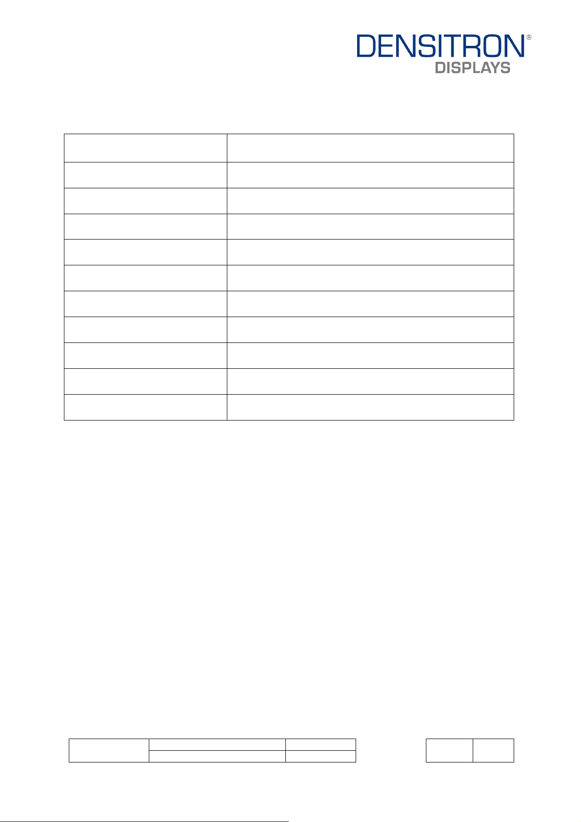
1 MAIN FEATURES
ITEM CONTENTS
Display Format 64 x 48 Dots
Overall Dimensions(W*H*T) 18.46 x 18.10 x 2.10 mm
Active Area(W*H) 13.42 x 10.06 mm
Viewing Area(W*H) 15.42 x 12.06 mm
Display Mode Passive Matrix (0.66”)
Display Colour Blue
Driving Method 1 / 48 duty
Driver IC SSD1305Z
Operating temperature
Storage temperature
-30℃ ~ +70℃
-40℃ ~ +80℃
Product No.
DENSITRON TECHNOLOGIES plc. – PROPRIETARY DATA – ALL RIGHTS RESERVED
DD-6448BE-2A REV. A
REV.
Page 4 / 27
Page 5

2 MECHANICAL SPECIFICATION
2.1 MECHANICAL CHARACTERISTICS
ITEM CHARACTERISTIC UNIT
Display Format 64 x 48 Dots
Overall Dimensions 18.46 x 18.10 2.10 mm
Active Area 13.42 x 10.06 mm
Viewing Area 15.42 x 12.06 mm
Dot Size 0.19 x 0.19 mm
Dot Pitch 0.21 x 0.21 mm
Weight 1.3 g
IC Controller/Driver SSD1305Z
Product No.
DENSITRON TECHNOLOGIES plc. – PROPRIETARY DATA – ALL RIGHTS RESERVED
DD-6448BE-2A REV. A
REV.
Page 5 / 27
Page 6

2.2 MECHANICAL DRAWING
Product No.
DENSITRON TECHNOLOGIES plc. – PROPRIETARY DATA – ALL RIGHTS RESERVED
DD-6448BE-2A REV. A
REV.
Page 6 / 27
Page 7

3 ELECTRICAL SPECIFICATION
3.1 ABSOLUTE MAXIMUM RATI NG S
Item Symbol Min Max Unit Note
Supply Voltage VDD -0.3 4 V
Supply Voltage for I/O
pins
VDDIO -0.3 VDD+0.5 V
Driver Supply Voltage VCC 0 15 V
Operating Temperature Top -30 70 °C -
Storage Temperature Tst -40 80 °C -
Static Electricity Be sure that you are grounded when handling displays.
Note 1: All the above voltage are on the basis of “GND=0V”.
Note 2: When this module is used beyond the above absolute maximum ratings, permanent
breakage of the module may occur. Also, for normal operations, it’s desirable to use
this module under the conditions according to Section 3 “Electrical Characteristics”.
If this module is used beyond these conditions, malfunctioning of the module can
occur and the reliability of the module may deteriorate.
3.1.1 Regarding the Gradation
Although this module possesses the gradation function, respective gradation levels will
vary depending on the production conditions etc. Also, the temperature range where the
grading function can be guaranteed will be -10~60°C.
Note 1,2
Product No.
DENSITRON TECHNOLOGIES plc. – PROPRIETARY DATA – ALL RIGHTS RESERVED
DD-6448BE-2A REV. A
REV.
Page 7 / 27
Page 8
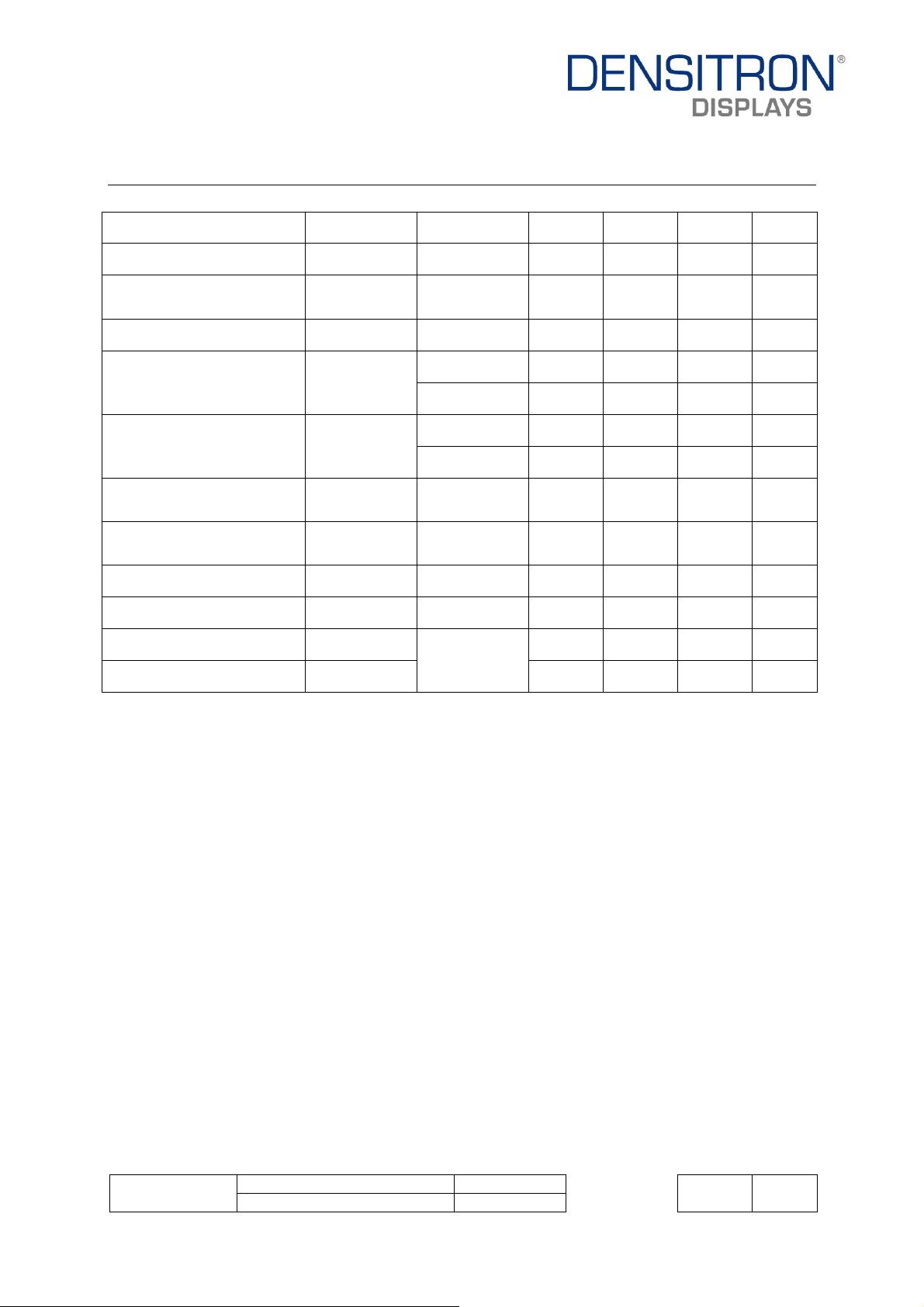
3.2 ELECTRICAL CHARACTERISTICS
3.2.1 DC CHARACTERISTICS
Characteristics Symbol Conditions Min Typ Max Unit
Supply Voltage VDD 2.6 2.8 3.5 V
Supply Voltage for I/O
pins
VDDIO 1.6 2.8 VDD V
Driver Supply Voltage VCC 8.5 9 9.5 V
Operating Current for
VDD & VDDIO
Operating Current for
VCC
Sleep Mode Current for
VDD & VDDIO
Sleep Mode Current for
VCC
IDD & DDIO
ICC
IDD & DDIO
SLEEP
ICC SLEEP
Note 1
Note 2
Note 1
Note 2
High Level Input VIH
Low Level Input VIL 0 -
High Level Output VOH
Low Level Output VOL
Iout=100µA,
3.3Mhz
-
-
-
-
-
-
0.8xVDD
0.9xVDD
0.1 0.2 mA
0.1 0.2 mA
1.5 2.2 mA
2.5 3.5 mA
- 10 µA
- 10 µA
- V
- VDD V
0 -
V
DD
0.2xVDD
0.1xVDD
V
V
Note1: VDD = 2.8V, VCC = 9V, Frame rate = 190Hz, contrast setting = 0x2D, 50% display
area turn on.
Note 2: VDD = 2.8V, VCC = 9V, Frame rate = 190Hz, contrast setting = 0x2D, 100% display
area turn on.
Product No.
DENSITRON TECHNOLOGIES plc. – PROPRIETARY DATA – ALL RIGHTS RESERVED
DD-6448BE-2A REV. A
REV.
Page 8 / 27
Page 9

INTERFACE PIN ASSIGNMENT
No. Symbol I/O Function
Reserved Pin (Supporting Pin).
1 N.C. -
2 VCC P
3 VSS P
4 VDD P
5 VDDIO P
6 BS1 I
7 BS2 I
8 CS I
9 RES I
10 D/C I
11 WR I
The supporting pins can reduce the influences from stresses on
the function pins.
Power Supply for OLE system.
This is the most positive voltage supply pin of the chip. It must
be connected to external source.
Ground for OLED panel.
This is a ground pin. It also acts as a reference for the logic pins,
the OLED driving voltages and the analog circuits. It must be
connected to external ground.
Power Supply for Core Logic operation
This is a voltage supply pin. It must be connected to external
source.
Power Supply for Interface Logic level.
This is a voltage supply pin. It should be match with
MCU interface voltage level. VDDIO must allways
be equal or lower than VDD
Communicating Protocol Select.
These pins are MCU interface selection input. See the following table:
I²C 6800-parallel 8080-parallel Serial
BS1 1 0 1 0
BS2 0 1 1 0
Note “0” is connected to VSS “1” is connected to
VDDIO
Chip Select.
This pin is the chip select input. The chip is enabled for MCU
communication only when CS# is pulled low.
Power Reset for Controller and Driver.
This pin is reset signal input. When the pin is low, initialization
of the chip executed.
Data/Command Control.
This pin is Data/Command control pin. When the pin is pulled high, the
input at D7~D0 is treated as display data. When the pin is pulled low,
the input at D7~D0 will be transferred to the command register. For
detail relationship to MCU interface signal, please refer to the Timing
Characteristics Diagrams.
Read/Write Select or Write
This pin is MCU interface input. When interfacing to a 68xx
series microprocessor, this pin will be used as Read/Write
(R/W#) selection input. Pull this pin to “High” for read mode
and pull it to “Low” for write mode.
When 80xx interface mode is selected, this pin will be the write
(W/R#) input. Data write operation is initiated when this pin is
pulled low and the CS# is pulled low.
Product No.
DD-6448BE-2A REV. A
REV.
Page 9 / 27
DENSITRON TECHNOLOGIES plc. – PROPRIETARY DATA – ALL RIGHTS RESERVED
Page 10
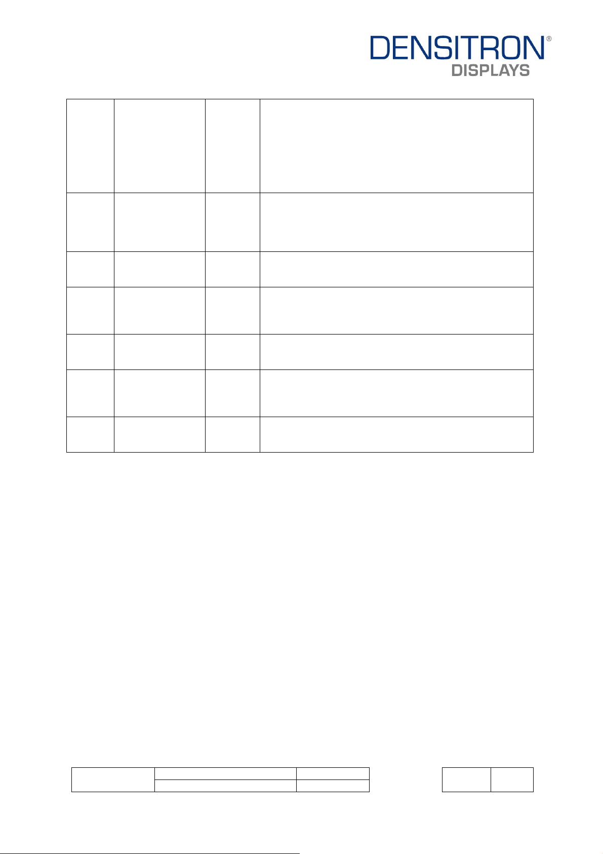
12 RD I
13~20 D0~D7 I/O
21 IREF I
22 VCOMH O
23 VCC P
24 VSS
25 NC
Read/Write Enable or Read.
This pin is MCU interface input. When interfacing to a 68xx
series microprocessor, this pin will be used as the Enable (E)
signal. Read/write operation is initiated when this pin is pulled
high and the CS# is pulled low.
When connecting to an 80xx microprocessor, this pin receives
the Read (RD#) signal. Data read operation is initiated when this
pin is pulled low and CS# is pulled low.
Host Data Input / Output Bus
These pins are 8 bit bi directional data bus to be connected to
the microprocessor’s data bus. When serial mode is selected, D1
with be the serial data input SDIN and D0 will be the serial
clock input SCLK.
Current Reference for Brightness adjustment
This pin is segment current reference pin. A resistor should be
connected between this pin and VSS. Set the current at 10µA
Voltage Output High Level for COM signal
This pin is the input pin for the voltage output high level for
COM signals. A capacitor should be connected between this pin
and VSS.
Power Supply for OLE sytem
This is the most positive voltage supply pin of the chip. It must
be connected to external source.
Ground for OLED panel.
This is a ground pin. It also acts as a reference for the logic pins,
the OLED driving voltages and the analog circuits. It must be
connected to external ground.
Reserved Pin (Supporting Pin).
The supporting pins can reduce the influences from stresses on
the function pins.
Product No.
DD-6448BE-2A REV. A
REV.
Page 10 / 27
DENSITRON TECHNOLOGIES plc. – PROPRIETARY DATA – ALL RIGHTS RESERVED
Page 11

3.3 BLOCK DIAGRAM
MCU Interface Selection: BS1 and BS2
Pins connected to MCU interface:D7~D0, RD, WR, D/C, RES and CS
C1, C3, C3, C4: 4.7μF
R1 : 910kΩ, R1 = ( Voltage at IREF – VSS ) / IREF
Product No.
DENSITRON TECHNOLOGIES plc. – PROPRIETARY DATA – ALL RIGHTS RESERVED
DD-6448BE-2A REV. A
REV.
Page 11 / 27
Page 12
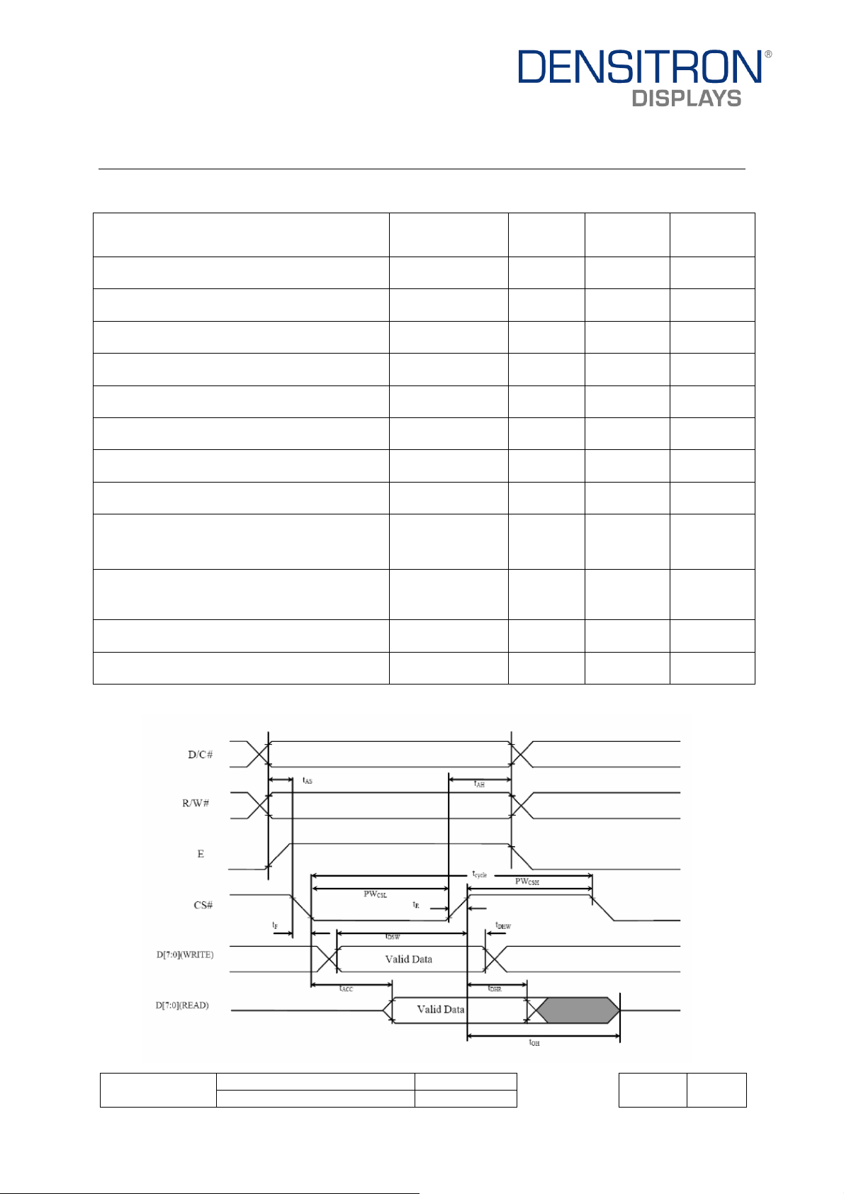
3.4 TIMING CHARACTERISTICS
3.5.1 AC CHARACTERISTICS
3.5.1.1 6800-Series MPU Parallel Interface Timing Characteristics:
Characteristics Symbol Min Max Unit
Clock Cycle Time t
300 - ns
cycle
Address Setup Time tAS 0 - ns
Address Hold Time tAH 0 - ns
Write Data Setup Time t
Write Data Hold Time t
Read Data Hold Time t
40 - ns
DSW
7 - ns
DHW
20 - ns
DHR
Output Disable Time tOH - 70 ns
Access Time t
Chip Select Low Pulse Width (Read)
Chip Select Low Pulse Width (Write)
Chip Select High Pulse Width (Read)
Chip Select High Pulse Width (Write)
- 140 ns
ACC
PW
PW
CSL
CSH
120
60
60
60
- ns
- ns
Rise Time tR - 15 ns
Fall Time tF - 15 ns
* VDD- VSS = 2.4 to 3.5V, Ta = 25˚C
Product No.
DENSITRON TECHNOLOGIES plc. – PROPRIETARY DATA – ALL RIGHTS RESERVED
DD-6448BE-2A REV. A
REV.
Page 12 / 27
Page 13
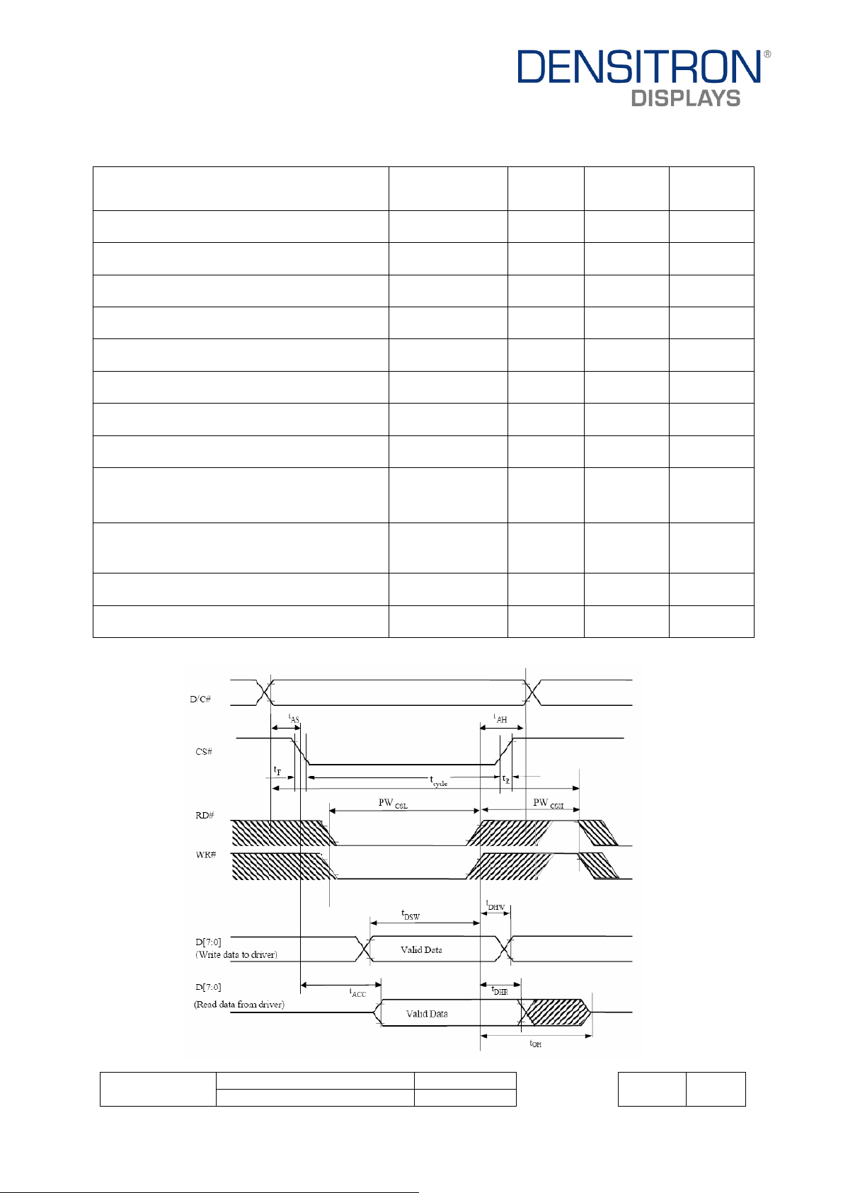
3.5.1.2 8080-Series MPU Parallel
Interface Timing Characteristics:
Characteristics Symbol Min Max Unit
System Cycle Time t
300 - ns
cycle
Address Setup Time tAS 0 - ns
Address Hold Time tAH 0 - ns
Write Data Setup Time t
Write Data Hold Time t
Read Data Hold Time t
40 - ns
DSW
7 - ns
DHW
20 - ns
DHR
Output Disable Time tOH - 70 ns
Access Time t
Chip Select Low Pulse Width (Read)
Chip Select Low Pulse Width (Write)
Chip Select High Pulse Width (Read)
Chip Select High Pulse Width (Write)
- 140 ns
ACC
PW
PW
CSL
CSH
120
60
60
60
- ns
- ns
Rise Time tR - 15 ns
Fall Time tF - 15 ns
* VDD~VSS = 2.4 to 3.5V, Ta = 25˚C
Product No.
DENSITRON TECHNOLOGIES plc. – PROPRIETARY DATA – ALL RIGHTS RESERVED
DD-6448BE-2A REV. A
REV.
Page 13 / 27
Page 14

3.5.1.3 Serial Interface Timing
Characteristics:
Characteristics Symbol Min Max Unit
Clock Cycle Time t
250 - ns
cycle
Address Setup Time tAS 150 - ns
Address Hold Time tAH 150
Chip Select Setup Time t
Chip Select Hold Time t
Write Data Setup Time t
Write Data Hold Time t
Serial Clock Low Time t
Serial Clock High Time t
120
CSS
60 - ns
CSH
50
DSW
15
DHW
100 - ns
CLKL
100 ns
CLKH
-
-
-
-
ns
ns
ns
ns
Rise Time tR - 15 ns
Fall Time tF - 15 ns
* VDD~VSS = 2.4 to 3.5V, Ta=25˚C
Product No.
DENSITRON TECHNOLOGIES plc. – PROPRIETARY DATA – ALL RIGHTS RESERVED
DD-6448BE-2A REV. A
REV.
Page 14 / 27
Page 15
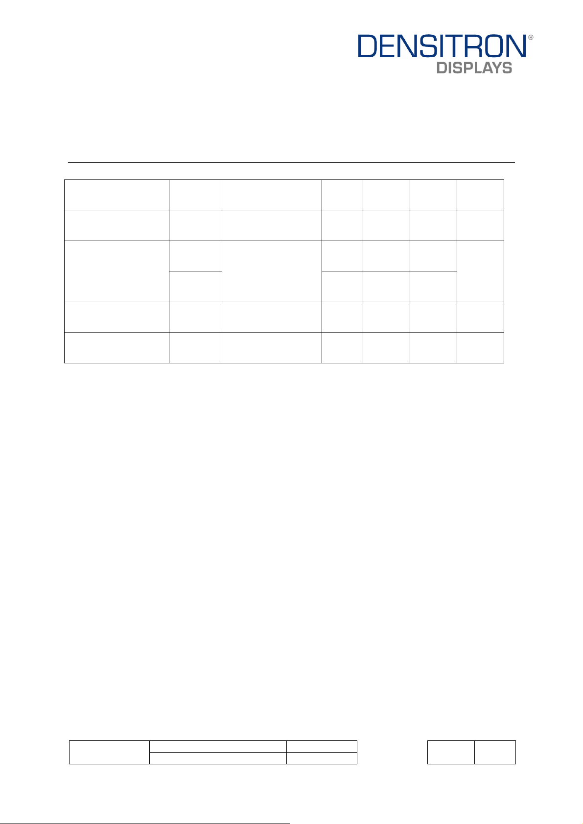
4 OPTICAL SPECIFICATION
4.1 OPTICAL CHARACTERISTICS
Characteristics Symbol Condition Min Typ Max Unit
Brightness Lbr With polarizer 40 60 - cd/m2
(X) 0.12 0.16 0.20
C.I.E.(Blue)
(Y)
Without Polarizer
-
0.24 0.28 0.30
Dark Room
Contrast
CR Shown as below - >1:100 - -
View Angle >160 - - degree
Note: Optical measurement taken at 1/48 duty 190Hz Frame rate, 0x2D contrast setting
Product No.
DENSITRON TECHNOLOGIES plc. – PROPRIETARY DATA – ALL RIGHTS RESERVED
DD-6448BE-2A REV. A
REV.
Page 15 / 27
Page 16

5 APPLICATION NOTES
5.1 COMMANDS
Please refer to the Technical Manual for the SSD1303.
5.2 POWER UP/DOWN SEQUENCE
To protect panel and extend the panel life time, the driver IC power up/down routine should
include a delay period between high voltage and low voltage power sources during turn on/off.
It gives the panel enough time to complete the action of charge and discharge before/after the
operation.
5.2.1 POWER UP SEQUENCE:
V
ON VCC ON Display On
DD
1. Power up VDD & VDDIO
2. Send Display off command VCC
3. Clear screen
4. Power up VCC VDD
5. Delay 100ms
(When VDD is stable) VSS/Ground
6. Send Display on command
5.2.2 POWER DOWN SEQUENCE:
Display off V
1. Send Display off command
2. Power down VCC VCC
3. Delay 100ms
(when VCC is reach 0 and panel is
completely discharges) V
4. Power down V
& VDDIO
DD
DD
VSS/Ground
off VDD off
CC
5.3 RESET CIRCUIT
When RES# input is low, the chip is initialized with the following status:
1. Display is off
2. 64x48 Display Mode
3. Normal segment and display data column and row address mapping (SEG0 mapped to
column address 00H and COM0 mapped to row address 00H)
4. Shift register data clear in serial interface
5. Display start line is set at display RAM address 0
6. Column address counter is set at 0
7. Normal scan direction of the COM outputs
8. Contrast control register is set at 80H
9. Normal display mode ( Equivalent to A4h command )
Product No.
DENSITRON TECHNOLOGIES plc. – PROPRIETARY DATA – ALL RIGHTS RESERVED
DD-6448BE-2A REV. A
REV.
Page 16 / 27
Page 17

5.4 APPLICATION EXAMPLE
Command usage and explanation of an actual example
< Initialization Setting >
Set Deactivate Scroll
(00101101 )
Set Pre Charge Period
( 11011001 with XXXXXXXX )
Set Contrast Control Register
(10000001 with XXXXXXXX )
Set Brightness for Colour Banks
(10000010 with XXXXXXXX )
Set Look Up Table (LUT)
(10010001 with **XXXXXX, **XXXXXX, **XXXXXX, **XXXXXX)
Set Area Colour Mode & Low Power Display Mode
(11011000 with 00XX0X0X)
00000101=>0x05 (Mono & Low Power Save Mode )
Set Segment Re-map
(1010000X)
Set COM Output Scan Direction
(1100X000)
Set COM Pins Hardware Configuration
(11011010 with 00XX0010)
00010010=> 0x12 (Alternative Mode)
Set Display Start Line
(01XXXXXX)
Set Display Offset
(11010011 with **XXXXXX)
Set Multiplex Ratio
(10101000 with **XXXXXX)
Set Display Clock Divide Ratio / Oscillator Frequency
(11010101 with XXXXXXXX)
Set DC/DC On/Off
(10101101 with 1000101X)
10001010=>0x8A (Off)
Set VCOMH Deselect Level
(11011011 with 0XXXXX00)
Set Entire Display On (1010010X)
10100100=> 0xA4 (Normal)
Set Normal/Inverse Display (1010011X)
10100110=>0xA6 (Normal)
Product No.
DENSITRON TECHNOLOGIES plc. – PROPRIETARY DATA – ALL RIGHTS RESERVED
DD-6448BE-2A REV. A
REV.
Page 17 / 27
Page 18

Set Display On/Off (1010111X)
10101111 => 0xAF (Turns On)
<Display Boundary Setting>
(00100000 with ******XX)
<Page Addressing Mode Setting>
Set Page Start Address for Page Addressing Mode (10110XXX)
10110000 =>0xB0
Set Lower Column Address for Page Addressing Mode
(0000XXXX)
Set Higher Column Address for page Addressing Mode
(0001XXXX)
<Horizontal or Vertical Addressing Mode Setting>
Set Column Address
(00100001 with XXXXXXXX, XXXXXXXX)
Set Page Address
(00100010 with *****XXX, *****XXX)
If the noise is accidentally occurred at the displaying window during the operation,
please reset the display in order to recover the display function.
Product No.
DENSITRON TECHNOLOGIES plc. – PROPRIETARY DATA – ALL RIGHTS RESERVED
DD-6448BE-2A REV. A
REV.
Page 18 / 27
Page 19
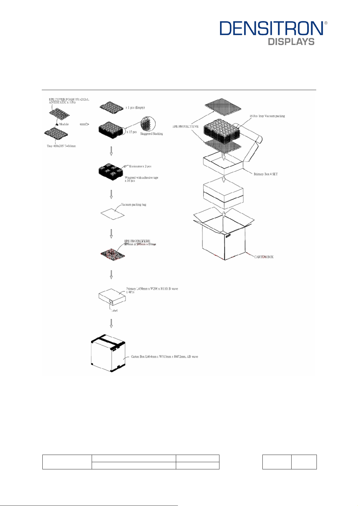
6 PACKAGING & LABELLING SPECIFICATION
6.1 PACKAGING
Product No.
DENSITRON TECHNOLOGIES plc. – PROPRIETARY DATA – ALL RIGHTS RESERVED
DD-6448BE-2A REV. A
REV.
Page 19 / 27
Page 20

6.2 LABELLING & MARKING
DENSITRON
DD-6448BE-2A
TW YY MM
Product No.
DENSITRON TECHNOLOGIES plc. – PROPRIETARY DATA – ALL RIGHTS RESERVED
DD-6448BE-2A REV. A
REV.
Page 20 / 27
Page 21
7 QUALITY ASSURANCE SPECIFICATION
7.1 CONFORMITY
The performance, function and reliability of the shipped products conform to the Product
Specification.
7.2 DELIVERY ASSURANCE
7.2.1 Delivery inspection standards
• IPC-AA610 class 2 electronic assemblies standard
7.2.2 Zone definition
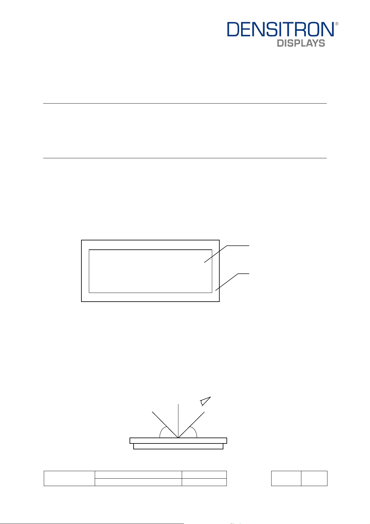
A Viewing area
B Outside viewing area
7.2.3 Visual inspection
• Inspect under 30W fluorescent lamp leaving 50 cm between the module and the lamp
and 30 cm between the module and the eye (measuring position).
• Appearance is inspected at the best contrast voltage (best contrast is adjusted
considering clearness and crosstalk on screen).
• Inspect the module at 45° right and left, top and bottom.
• Use the optimum viewing angle during the contrast inspection.
eye
45°45°
Product No.
DENSITRON TECHNOLOGIES plc. – PROPRIETARY DATA – ALL RIGHTS RESERVED
DD-6448BE-2A REV. A
REV.
Page 21 / 27
Page 22

7.2.3.1 Standard of appearance inspection
Units: mm
Class Item Criteria
Minor Outside & inside package Presence of product no., lot no., quantity
Critical
Major Dimension Product dimensions must be according to specification and drawing
Major Electrical Product electrical characteristics must be according to specification
Critical OLED
Minor Black spot,
Minor Polariser
Packing &
Label
Display
white spot,
dust
scratch
bubble
Product must not be mixed with others and quantity must not be different from
that indicated on the label
Missing lines or wrong patterns on display are not allowed
Round type: as per following drawing
∅ = (X+Y)/2
Acceptable quantity
Size Zone A Zone B
Line type: as per following drawing
Acceptable quantity
Length Width Zone A Zone B
- - W≤0.05 Any number
L≤2.0 W≤0.1 3
L>2.0 0
Total acceptable quantity: 3
Scratch on protective film is permitted Minor Polariser
Scratch on polariser: same as No. 1
∅ = (X+Y)/2
Acceptable quantity
Size Zone A Zone B
Total acceptable quantity: 3
∅<0.1
0.1<∅<0.2
0.2<∅<0.25
0.25<∅
∅<0.5
∅>0.5
Any number
3
1
0
Any number
0
Any number
Any number
Any number
Product No.
DENSITRON TECHNOLOGIES plc. – PROPRIETARY DATA – ALL RIGHTS RESERVED
DD-6448BE-2A REV. A
REV.
Page 22 / 27
Page 23
Class Item Criteria
Minor Segment
deformation
Minor Panel
Chipping
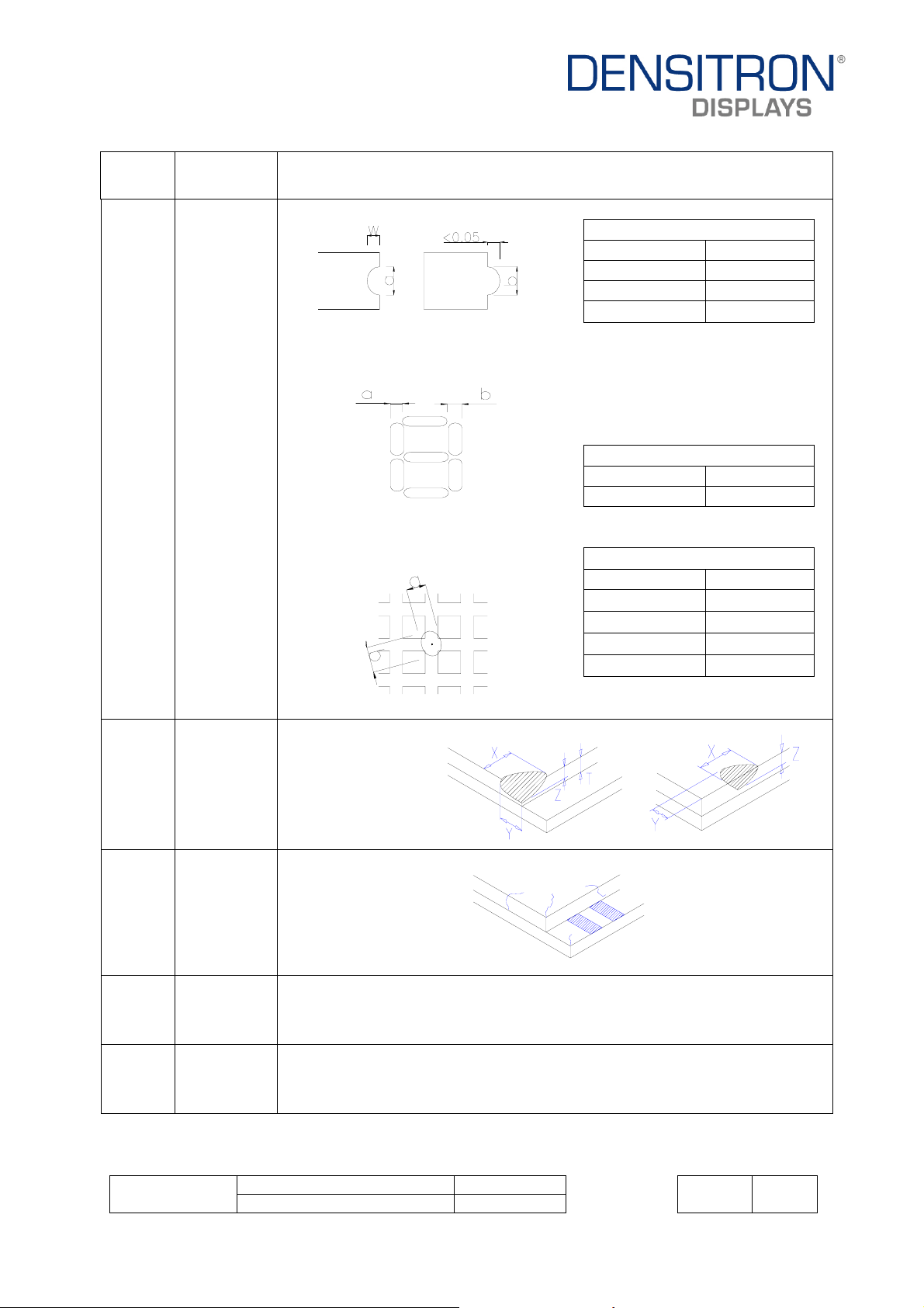
1b. Pin hole on dot matrix display
Acceptable quantity
Size
a,b<0.1 Any number
(a+b)/2≤0.1 Any number
0.5<∅<1.0
3
Total acceptable quantity: 7
2. Segments / dots with different width
Acceptable
a≥b a/b≤4/3
a<b a/b>4/3
3. Alignment layer defect
∅ = (a+b)/2
Acceptable quantity
Size
∅≤0.4
0.4<∅≤1.0
1.0<∅≤1.5
1.5<∅≤2.0
Total acceptable quantity: 7
Any number
5
3
2
X ≤ 1/6 Panel length
Y ≤ 1
Z ≤ T
Minor Panel
Cracking
Minor Cupper
Cracks not allowed
Not allowed if visible by eye inspection
exposed
(pin or film)
Minor Film or
Not allowed if affects electrical function
Trace
Damage
Product No.
DD-6448BE-2A REV. A
REV.
Page 23 / 27
DENSITRON TECHNOLOGIES plc. – PROPRIETARY DATA – ALL RIGHTS RESERVED
Page 24

Class Item Criteria
Minor Contact
Lead Twist Not allowed
Minor Contact
Lead
Not allowed
Broken
Minor Contact
Lead Bent
Not allowed if
bent lead causes
short circuit
Not allowed if bent lead
extends horizontally
more than 50%
of its width
Minor Colour
Level of sample for approval set as limit sample
uniformity
Major No unmelted solder paste should be present on PCB
PCB
Critical Cold solder joints, missing solder connections, or oxidation are not allowed
Minor No residue or solder balls on PCB are allowed
Critical
Minor Tray
particles
Short circuits on components are not allowed
Size Quantity
On tray
On display
∅<0.2
∅>0.25
∅≥0.25
L = 3 1
Any number
4
2
Product No.
DD-6448BE-2A REV. A
REV.
Page 24 / 27
DENSITRON TECHNOLOGIES plc. – PROPRIETARY DATA – ALL RIGHTS RESERVED
Page 25

7.3 DEALING WITH CUSTOMER COMPLAINTS
7.3.1 Non-conforming analysis
Purchaser should supply Densitron with detailed data of non-conforming sample.
After accepting it, Densitron should complete the analysis in two weeks from receiving the
sample.
If the analysis cannot be completed on time, Densitron must inform the purchaser.
7.3.2 Handling of non-conforming displays
If any non-conforming displays are found during customer acceptance inspection which
Densitron is clearly responsible for, return them to Densitron.
Both Densitron and customer should analyse the reason and discuss the handling of nonconforming displays when the reason is not clear.
Equally, both sides should discuss and come to agreement for issues pertaining to
modification of Densitron quality assurance standard.
Product No.
DENSITRON TECHNOLOGIES plc. – PROPRIETARY DATA – ALL RIGHTS RESERVED
DD-6448BE-2A REV. A
REV.
Page 25 / 27
Page 26
8 RELIABILITY SPECIFICATION
8.1 CONTENTS OF RELIABILITY TESTS
Test Item Test Condition Evaluation and assessment
High Temperature Operation 70°C±2, 240 hours
Low Temperature Operation -30°C±2, 240 hours
High Temperature Storage 80°C±2, 240 hours
Low Temperature Storage -40°C±2, 240 hours
High Temperature & High
Humidity Storage
60°C±2, 90%RH, 240 hours
No abnormalities in function
and appearance
No abnormalities in function
and appearance
No abnormalities in function
and appearance
No abnormalities in function
and appearance
No abnormalities in function
and appearance
24 cycle of
Thermal Shock
-40°C 60 min,
R.T. 5 min,
No abnormalities in function
and appearance
85°C 60 min
* The brightness should be greater than 50% of the initial brightness.
* The samples used for the above tests do not include polarizer.
* No moisture condensation is observed during tests.
8.2 LIFE TIME
Item Description
Function, performance, appearance, etc. shall be free from remarkable deterioration
more than 10,000 hours under ordinary operating and storage conditions of room
1
temperature (25±10 °C), normal humidity (45±20% RH), and in area not exposed to
direct sunlight.
2 End of lifetime is specified as 50% of initial brightness.
The storage period is warrantable of more than 20,000hr from the date of invoice
under normal room conditions as stated below.
3
Temperature: 23 ± 5°C. Humidity: 55 ± 15 %RH.
In case of the seal of cartoon not opened
8.3 FAILURE CHECK STANDARD
After the completion of the described reliability test, the samples wewe left at room
temperature for 2 hrs prior to conducting the failure teat at 23±5 °C;55±15% RH.
Product No.
DENSITRON TECHNOLOGIES plc. – PROPRIETARY DATA – ALL RIGHTS RESERVED
DD-6448BE-2A REV. A
REV.
Page 26 / 27
Page 27

9 HANDLING PRECAUTIONS
Safety
If the panel breaks, be careful not to get the organic substance in your mouth or in your eyes.
If the organic substance touches your skin or clothes, wash it off immediately using soap and plenty of
water.
Mounting and Design
Place a transparent plate (e.g. acrylic, polycarbonate or glass) on the display surface to protect the
display from external pressure. Leave a small gap between the transparent plate and the display
surface.
Design the system so that no input signal is given unless the power supply voltage is applied.
Caution during OLED cleaning
Lightly wipe the display surface with a soft cloth soaked with Isopropyl alcohol, Ethyl alcohol or
Trichlorotriflorothane.
Do not wipe the display surface with dry or hard materials that will damage the polariser surface.
Do not use aromatic solvents (toluene and xylene), or ketonic solvents (ketone and acetone).
Caution against static charge
As the display uses C-MOS LSI drivers, connect any unused input terminal to V
input any signals before power is turned on.
Also, ground your body, work/assembly table and assembly equipment to protect against static
electricity.
Packaging
Displays use OLED elements, and must be treated as such. Avoid strong shock and drop from a
height.
To prevent displays from degradation, do not operate or store them exposed directly to sunshine or
high temperature/humidity.
Caution during operation
It is indispensable to drive the display within the specified voltage limit since excessive voltage
shortens its life.
Other Precautions
When a display module is operated for a long of time with fixed pattern may remain as an after image
or slight contrast deviation may occur.
Nonetheless, if the operation is interrupted and left unused for a while, normal state can be restored.
Also, there will be no problem in the reliability of the module.
Storage
Store the display in a dark place where the temperature is 25°C ± 10°C and the humidity below
50%RH.
Store the display in a clean environment, free from dust, organic solvents and corrosive gases.
Do not crash, shake or jolt the display (including accessories).
or VSS. Do not
DD
Product No.
DD-6448BE-2A REV. A
REV.
Page 27 / 27
DENSITRON TECHNOLOGIES plc. – PROPRIETARY DATA – ALL RIGHTS RESERVED
 Loading...