

Page 1
Model:
NBLNA33
NBLNA23
Gain:
17dB nominal
16dB nominal
Frequency Range
902-928 MHz
1280 – 1300 MHz
Noise Figure:
<0.5dB
<0.5dB
P1dB without Damage
+13dBm output
+13dBm output
Input VSWR:
>6dB 500 - 3500 MHz
>6dB 500 - 3500 MHz
Output VSWR:
>10dB @ design frequency
>10dB @ design frequency
Voltage:
+7 - +22 VDC
+7 - +22 VDC
Current Drain
70 mA nominal
70 mA nominal
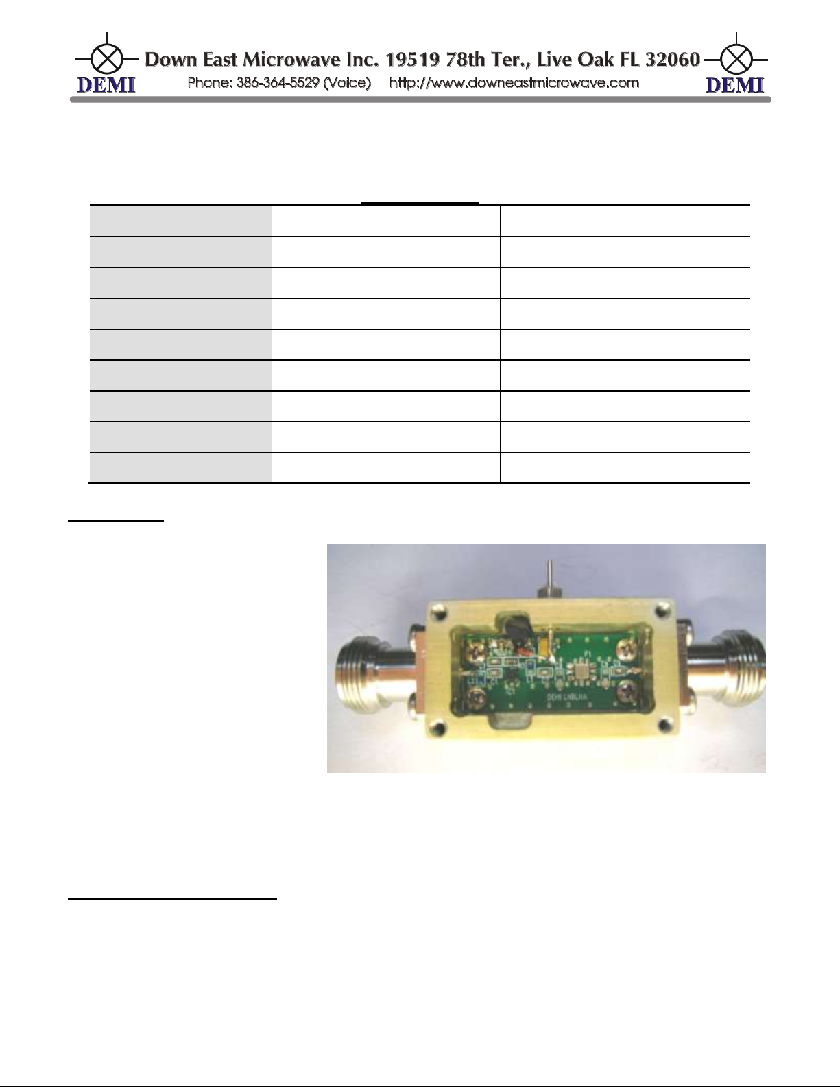
DEM NBLNA33 and NBLNA23
Low Noise Amplifier
Specifications:
Description:
The DEM NBLNA33 and
NBLNA23 is a new design
utilizing the combination of
PHEMT and SAW filter
technology to produce a LNA that
is very immune to out of band
interference. The active
component is the QORVO
TQP3M9037 MMIC amplifier.
The difference between the two
models is the selection of the
Band Pass filters. The LNA’s do
not offer any RF bypass
switching for transceiver operation and therefore may only be utilized in receive only
applications. It is offered with a robust machined enclosure and various types of RF connectors
and connector combinations to allow any LNA to be “dropped in” to any pre-existing system or is
ready to be a component in a newly developed receive system.
Installation and Operation:
Depending on your application, the LNA may be installed anywhere in your system to
increase gain. To maintain or improve the systems noise figure requires the LNA to be installed
as close to the systems antenna as possible. If you plan to utilize this LNA in a transceive
system with transmit bypass relays, be sure of their isolation characteristics and transmit power
handling capabilities before transmitting. Use only interconnecting cables and/or adapters that
are rated for use at or above the intended frequency of use. Inadequate cabling or cables with
/Manuals/Built/LNA/NBLNA23_33.docx 1 8/10/2022
Page 2
+DC
C6
C4
C3
C1
C2 C5
L1
VR1
L2
IN
OUT
F
IC1
poor shielding may cause system instabilities, signal loss, or undesirable intermittent operation.
Test any sequenced scheme before applying transmit power to avoid mishaps.
The connector marked IN (Input), is to be connected to the antenna side of the system.
The OUT (Output) is connected to the receiver side of the system. Expected performance with
the LNA correctly installed should be overall improvement in gain and system noise figure of the
receive system. The proper installation of an LNA becomes more important if you make this
installation in a harsh RF environment. The gain bandwidth of the LNA is just wide enough at the
specified operating frequency to obtain a low noise figure. This still may result in the passing of
strong but “close in frequency” out of band signals that may cause the overloading of your
receiver resulting in increased inter-modulation. This new design utilizes a SAW band pass filter
in the output circuit that will eliminate all but the strongest of interferences.
Be sure both input and output ports are terminated before applying DC voltage to the
LNA. If you desire to pre-test the LNA in a test bench environment before installation, because
of the SAW filters dissipation factor, do not apply more than -10dBm to the input if testing linear
response. At levels above -10dBm, expect some gain compression. The input is protected with a
DC path to ground to eliminate static build up from rain or wind but may not survive levels of
EMP developed by lightning. Please use standard lightning protection for all installations.
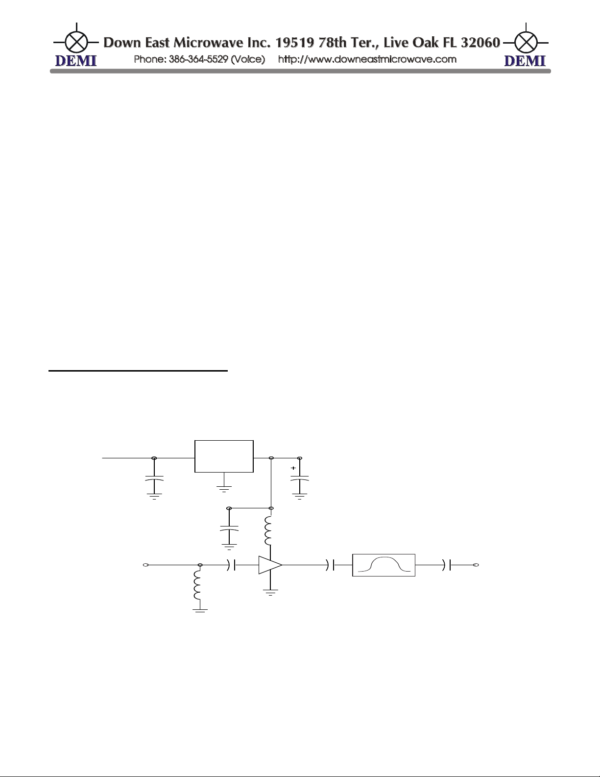
Schematic Diagram and Layout:
/Manuals/Built/LNA/NBLNA23_33.docx 2 8/10/2022
 Loading...