

Page 1
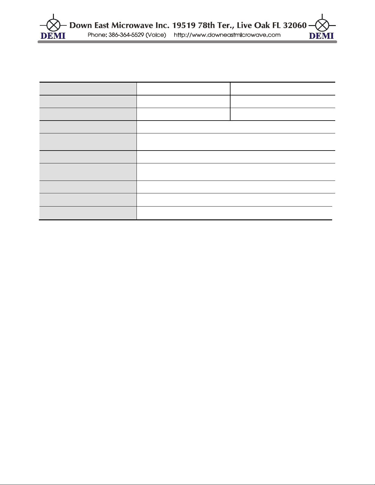
DEM Part Number 5760-144_____
Power Out:
>2.5 W adjustable
LP version: > 10 mW
Noise Figure and Gain:
<1.5dB @ 17dB G
<3.5dB
DC Power Requirement:
10 - 15.5 VDC @ 2.5 Amp
<0.6 Amp
IF Option:
Common Split
IF Drive Level
Requirement:
1-250 mW 250mW-3W 3-10W Other_____________
Keying Option:
PTT - to ground TTL - Positive Voltage
Aux. Connection Outp ut
Option:
TX RX High Low RVD
Antenna Option:
Common Separate TX & RX
EXT.10 MHz Source Level:
+3dBm +/- 6db (Terminate the port when not in use)
OPTIONS:
5760 MHz. Transverter, __________ MHz IF, SN__________
Operational Overview
The DEM 5760-144 is a 5 cm to 144 MHz transmit and receive converter. It has a linear
output power of >2.5 watts ( > 10mW for LP version) and may be achieved with as little as 10mW
or a maximum of 10 W of IF drive with the correct IF configuration. The receive section is a
design using a PHEMT LNA (GaAs MMIC in the LP).
The base local oscillator frequency is provided by Q5 Signal DigiLO synthesizer. It has a
internal 10 MHz clock or can be used with a external clock. The DEM 5760-144 has a built in
transmit / receive relay driver to provide voltages required by common SMA relays and provisions
for external switching so adding a high power amplifier or preamplifier to your 5cm system is easy.
TXIF level options have been built into the transverter. The IF levels are adjustable on both
transmit and receive and have a dynamic range of approx. 25dB. This is useful for adjusting your
maximum output power and setting the "S" meter level on your IF receiver. The IF connections are
via BNC connectors.
Options have been provided for a key line input PTT-H (+1 to 15 VDC) or PTT-L (a closure
to ground) and auxiliary contacts on either transmit or receive with a common line for many
applications. The control, power, and auxiliary connections are via DC feed thru connectors and
the 5cm connectors are SMA. T he 576 0-144 is housed in our standard 4.125" x 1.875" x 9.75"
extruded aluminum enclosure that matches the all of our other microwave transverters.
Connect your transceiver to the transverter:
Interfacing the transverter to the transceiver is easy. First review the assembled
configuration above. If the transverter was configured for direct connection to your transceiver (10
watts or less), follow the steps listed next.
1. Open the top lid of the transverter by removing 4 screws.
/Built/5760-144rC.docx 1 Rev. C 10/24/2019
Page 2

2. Connect all IF cables. The transverter may have a common IF port or two separate ports TXIF
and RXIF. Use good quality coax cable to connect the ports between your transceiver and the
IF connectors on the transverter.
3. Connect the Push to Talk line out of your transceiver to the transverter. It is labeled PTT on the
transverter and uses a solder type DC feed through connector. The correct keying type can be
configured for your transceiver at time of order or you may select it in the transverter now by
moving the PTT jumper on the TC board.
4. If the WTR option was not ordered, you will have separate TX and RX ports. You may connect
your own transfer relay at this time or continue interfacing without it. Connect your 5cm antenna
system or a dummy load with a power meter to the appropriate transverter ports. Always
terminate the receive port with a 50 ohm load.
5. Connect the external 10 MHz clock if you desire. Not required for testing or use.
6. Connect the DC power to the transverter. It uses a DC feed through type connector. 13.8 volts
is optimum but the transverter will operate normally from 11 to 15 volts.
7. Preset the TXIF gain control fully counter-clockwise and the RXIF gain control fully clockwise in
the transverter. This is max i mu m atten uat ion on Transmit and minim um atte nu ati on on Receive.
8. Power your transceiver “ON”. The green "ON" LED will be lit and either a red or green “Lock”
LED should be lit. Green is when an external 10 MHz source is connected. The TX LED should
not be lit. Set your Transceiver set to 144.100 MHz. This should be 5760.100 unless you
ordered a different frequency scheme.
9. Adjust the RXIF gain control until a slight noise increase is heard in the transceiver or just a
slight movement in the “S” meter is detected. Power the transverter on and off to verify the
change of noise in the transceiver. You may also remove the 50 ohm load to determine receiver
performance. Find a signal on the band or use a signal generator to determine correct
frequency, or minimum signal level desired. If you are planning on installing an external LNA
you may adjust the IF level after installation.
10. It is recommended to test the transverter in the CW mode because most transceiver s have
carrier level controls in this mode only. Do not use full or semi break-in if possible. Do not use
FM , SSB or AM because it may not be possible to obtain maximum output power with your
transceiver in these modes. Set the carrier/output power control on your transceiver to
minimum or “0” output power. Place the transceiver into transmit. If the PTT circuit is
connected correctly, the transmit LED on the transverter will switch on. While observing a
power meter on the 5cm system, slowly increase the carrier control (with key down) or increase
the power output control to 10 watt maximum on the transceiver. If the transverter is configured
correctly for your transceiver, minimal power may be detected on the power meter. Slowly adjust
the TXIF control in the transverter in a clockwise direction while observing the power meter. Set
it to obtain a saturated power reading and then just back off a little to avoid total saturation. If a
power meter is not available this will be difficult. You may use a current meter on the DC power
line to determine if the transverter is transmitting with the 3 watt unit only. A maximum of 2.5
amps should be obtainable and it should not vary as the TXIF control is adjusted. When
maximum power is achieved the current will suddenly decrease. This is saturation. Back off the
TXIF drive to limit the amount of saturation. Switch the transceiver to USB and make a
transmission. The power output and current drain should correlate to your speech pattern.
11. You may re-adjust both RXIF and TXIF again if desired. Do not adjust any of the filters unless
you have access to a spectrum analyzer at minimum. It is also not recommended to adjust the
bias pots of the LNA and power amplifier in the 3 watt unit. They have been optimiz ed.
12. Put the top on the enclosure and install the screws. Your transverter system is ready to use.
Connect as you wish to use it in your 5cm system and have fun!
/Built/5760-144rC.docx 2 Rev. C 10/24/2019
Page 3
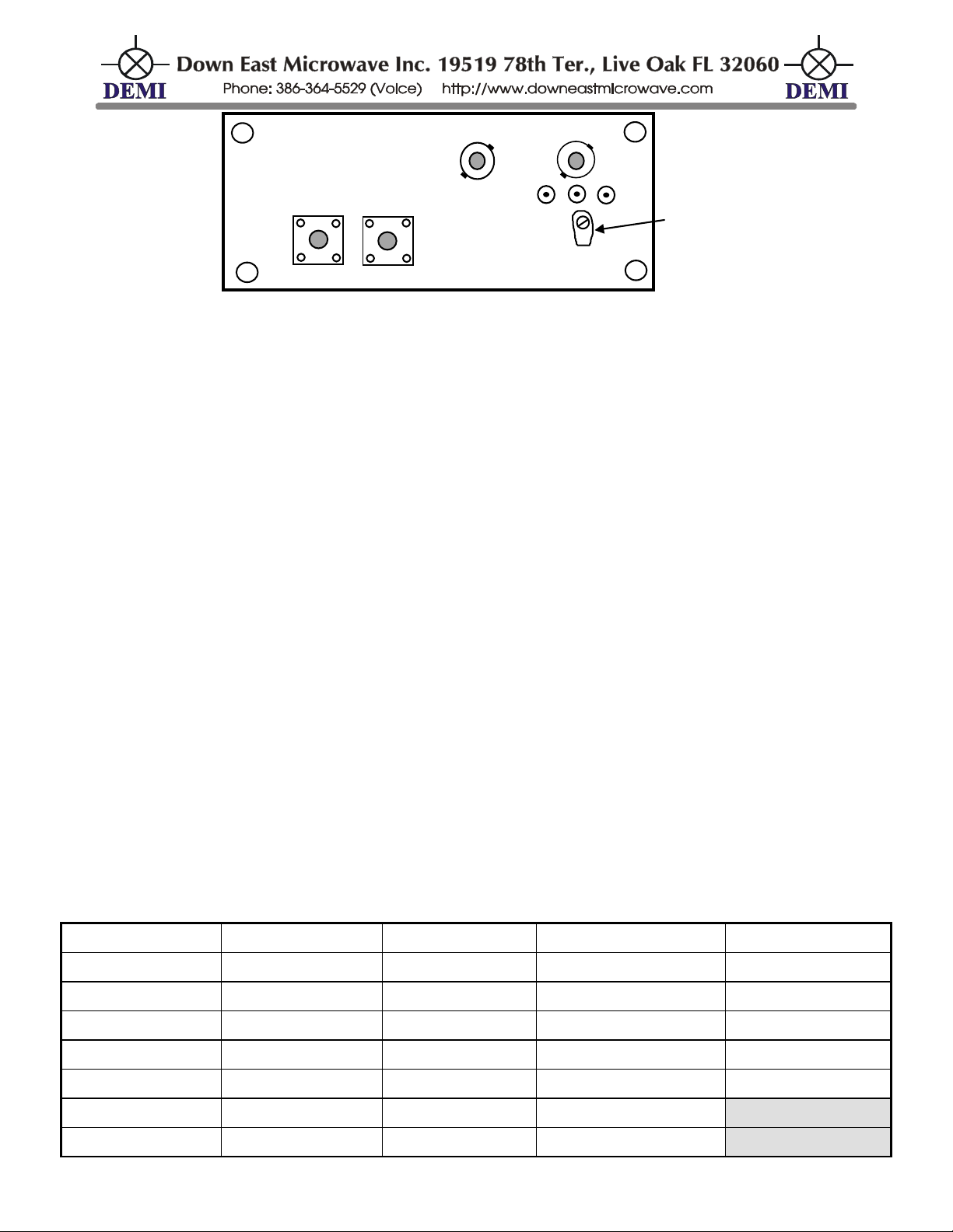
TX
RX
PTT +13.8VDC AUX
GND
IF
10 MHz
C1 100 pF
C12 5pF (0805)
C21 100 pF
U1 ERA-1
C2 5pF (0805)
U2 ERA-1
C14 100 pF
U4 N6
D1 HSMS2822
U5 N6
C17 5pF (0805)
D2 HSMS2822
U6 MGA86576
C6 100 pF
C18 5pF (0805)
2” #24 enamel
C7 5pF (0805)
C19 5pF (0805)
C11 5pF (0805)
DEM 5760 - 144 User Options:
Auxiliary Switching contacts:
The auxiliary contacts on the TC board (see the TC document) are labeled C (common) NO
(normally open) and NC (normally closed). The C connection can be wired to ground or +13.8
VDC. This will then be connected or dis-connected depending on if the transverter is in transmit or
receive. The contacts are marked for the receive mode. The NO or NC can be wired to the AUX
connector on the enclosure.
PTT options:
Both P T T-H and PTT-L can be changed on the top side of the TC board. The connections
are located in the center of the board near the connector panel. Change the jumper as required
from the PTT connection to either “L” (Ground to transmit) or “H” (Apply positive voltage to
transmit)
IF options:
All possible IF configurations are shown in the TC document and in the supplied schematic.
Follow the schematic and component list for changing the desired drive level ranges if you require
a different configuration or drive level. Splitting the IF to separate TX and RX is also explained.
Other combinations and drive levels may work but do not exceed 10 Watts input. The minimum TX
drive level for without damaging the TX mixer diode is 20 mW. Do not exceed this level and try to
limit the drive to 10 mW for a safety margin.
Frequency Options:
For other frequency options see the attached DigiLO synthesizer document.
5760 -144LP Transverter Board Compone nt List
All components are Surface Mount
R4 51 Ω
C3 0.1 µF
C4 0.1 µF C16 0.1 µF
C5 0.1 µF
/Built/5760-144rC.docx 3 Rev. C 10/24/2019
C13 0.1 µF C22 0.1 µF R8 51 Ω
C23 0.1 µF R9 36 Ω
R10 51 Ω
R11 130 Ω (LP opt)
R1 51 Ω R12 51 Ω
R2 82 Ω R13 100 Ω
C20 0.1 µF R3 82 Ω R24 36 Ω
Page 4
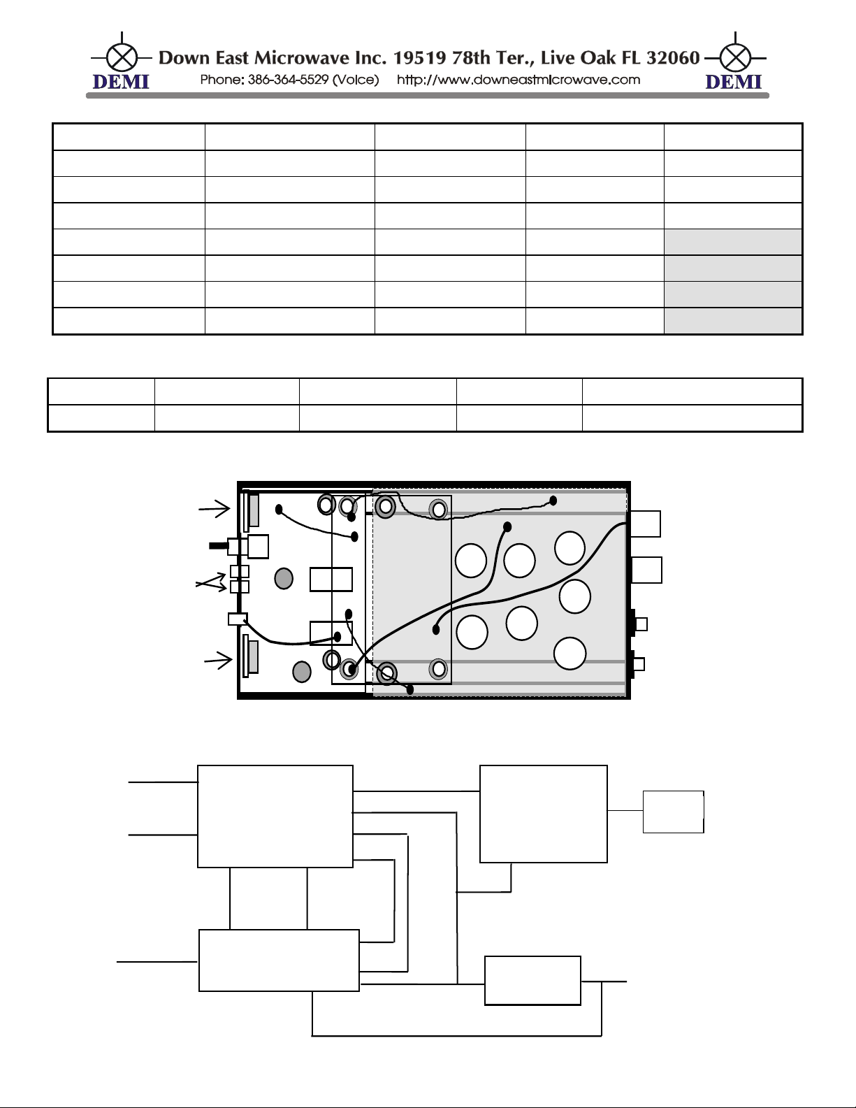
5760-144 LNA and Power Amplifier Section
C26 0.1 µF
C35 2.7 pF 50mil
C43 10.0 µF
R15 10 Ω(0805)
R23 36 Ω
C27 100
C36 5pF (0805)
VR1 78M05
D3 MMBD914
C30 100
IC1 FMM5056VF
4-40 Feed Thru
C31 10.0 µF
C39 0.1 µF
IC2 NMA0505S
R19 5.1K Ω
C32 2.7 pF 50mil
Q1 CE3512K2
C33 2.7 pF 50mil
Q2 MMBT3904
C34 2.7 pF 50mil
5760-144LP
5-3/4” Pipe caps
5-8-32 plated nuts
12-brass pins
5-8-32x 5/8” Brass screws
5760-144
7-3/4” Pipe caps
7-8-32 plated nuts
16-brass pins
7-8-32x 5/8” Brass screws
IF
SMA
TX
Load
Switch
LED
TC
PCB
RX
10 MHz
Synt
9V Reg.
+9
+9
RF Out
RX
TX
Lock LED
Lock
+9 VDC
RX IF
+TX
+RX
5760 Transverter PCB
M2
M1
TX IF
IF
10W Max.
+13.8VDC
Synth
9V Reg.
DEM TC
5616 MHz. LO
TX RF
RX RF
+LO
10 MHz
External or
Internal
C44 10.0 µF R16 51 Ω
C28 10.0 µF C37 0.1 µF
C38 0.1 µF
C40 0.1 µF
C41 10.0 µF
C42 10.0 µF R14 200 Ω pot R22 1K Ω pot
R17 51 Ω 3 Ω 10W
R18 220 Ω
R20 5.1K Ω
R21 5.1K Ω
FILTER COMPONENTS
/Built/5760-144rC.docx 4 Rev. C 10/24/2019
Page 5
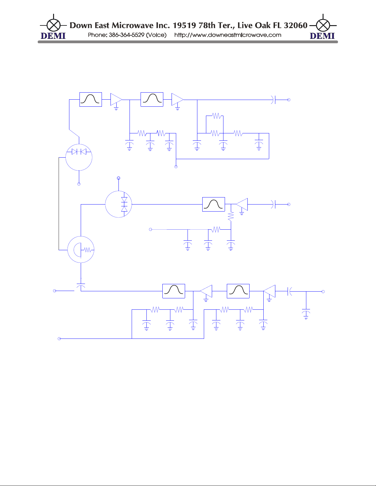
C18
U5
F4
U4
F3
C12
C13
C14
R8 R9
C17 C16
R10
R11 ( optional - LP only)
D1
D2
R7
F5
U6
C19
R12
R13
C22
C21 C20
C11
F2
U2
F1
U1
R3
R4
R2 R1
C5 C6
C7 C4 C3 C2
C1
+LO
INPUT
LO TP
+LO
+RX
RX IN
RX IF
TX IF
+TX
TX OUT
5760-144LP TRANSVERTER SCHEMATIC
C15
C24
R14
/Built/5760-144rC.docx 5 Rev. C 10/24/2019
Page 6
/Built/5760-144rC.docx 6 Rev. C 10/24/2019
Page 7
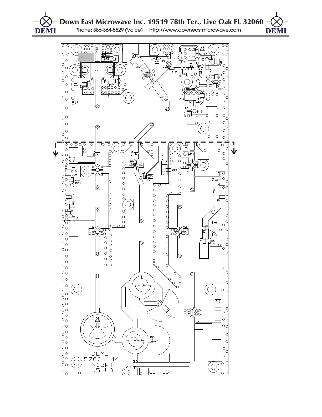
5
7
6
0
M
H
z
T
r
a
n
s
v
e
r
t
e
r
T
o
p
A
s
s
e
m
b
ly
L
a
y
o
u
t
N
O
T
E
-
R
1
4
,
R
2
2
,
I
C
2
A
N
D
F
1
-
7
A
R
E
L
O
C
A
T
E
D
O
N
T
H
E
B
O
T
T
O
M
S
I
D
E
O
F
T
H
E
P
C
B
O
A
R
D
.
LP
LP
A
C
5
Cut
Wire Jumper
Cut
Trim
Copper
Fo il
Cut
F5
F4
F3
F2
F1
F6
F7
/Built/5760-144rC.docx 7 Rev. C 10/24/2019
Page 8
TC PCB TOP
C16
DEM Part Number TCK
DEM TRANSVERTER CONTROL
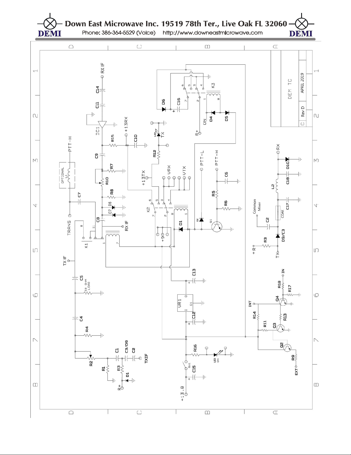
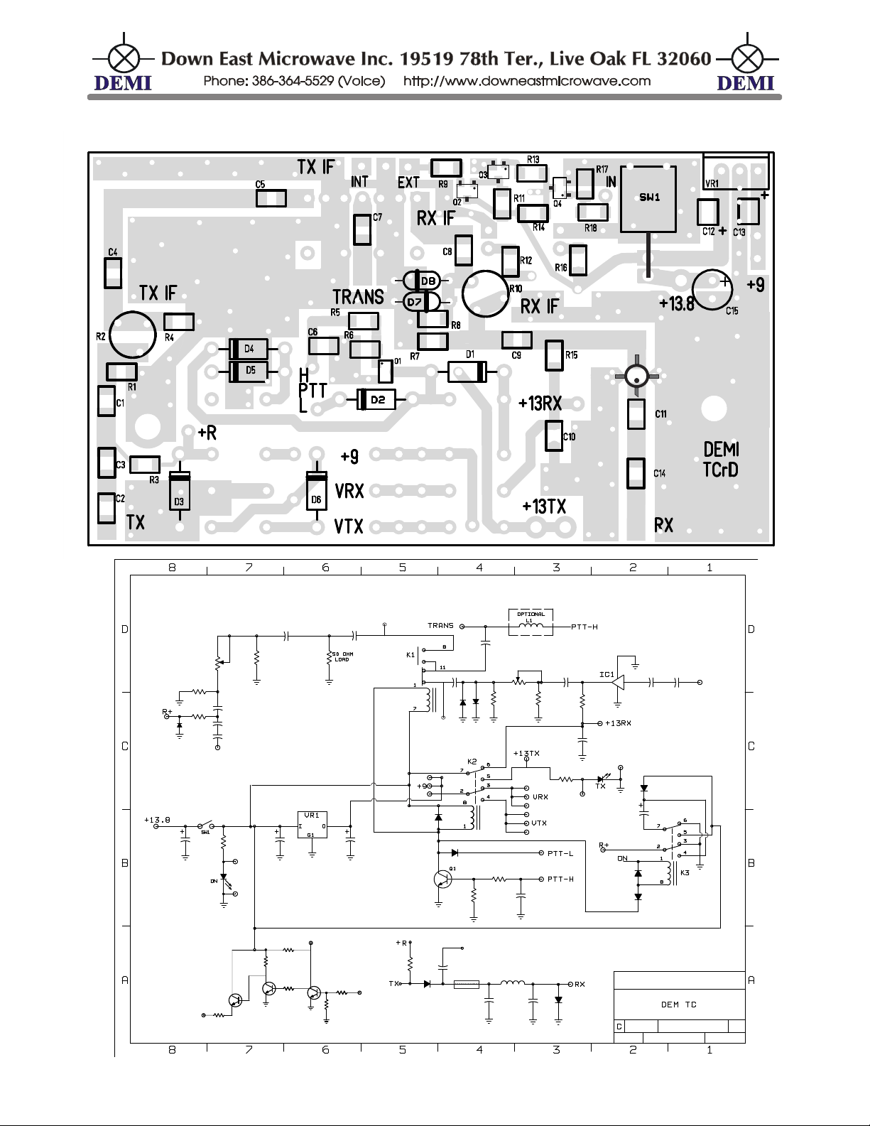
The DEM Transverter Control (DEM TC) was redesigned in 2019. to perform with both
separate IF and common IF microwave transverter boards or Mixers and to accommodate the
connections for the DIGILO synthesizer such as frequency switching and “LOC” indication. It is still
our basic “TC” board with the extra hooks incorporated. It is used in every DEMI microwave
transverter 2304 and up and provides the regulated +9VDC, IF switching and attenuation
functions, DC switching functions and external 24 VDC relay driver.
Circuit Description:
The DEM TC circuit board measures 3.75" x 2.15", which is designed to fit all DEMI
microwave enclosures.
The TC offers all of the functions our microwave transverters require such as providing a common
or split IF operation with up to a 10 watt IF drive level with either a PTT High or Low for keying. It
also incorporates adjustable attenuators for both transmit and receive and has an option for
additional receive gain if required. It will perform all dc switching functions for the transverter
including switching 24 VDC microwave relays. A new optional feature in the TC includes a PIN
diode switch network that connects the TC to a single mixer transverter while still allowing the TX
and RX gain to have independent adjustments. With this new design, the TC is more versatile and
will accommodate other makes of microwave transverters or offer more flexibility for homebrew
equipment.
It is not designed to be a drop in replacement for the original TC board.
Construction:
Before construction, read the complete document and review the component placement
document and schematic. Depending on your system design, or the type of transceiver to be
used, you will need to make a few decisions about the assembly of the TC.
Most components are thru-hole except for IC1, SMD capaci t or s and Pi n dio des use d for
common mixer transverters. All DEMI transverters will need the standard TC and not the common
mixer configuration. The common mixer configuration will be shown at the end of the document.
Referring to the provided schematic, parts list, and component pl a ce me nt di ag r am, i nstall and
solder all components in this order: All leaded components, R1- R3, R5 - R12, D1 – D8, C9-C11
and Q1 on the topside.
Install K1 and C16 on the bottom side of the PCB. Refer to the pictorial for the installation of C16
and check it’s polarity. This capacitor is mounted so that the case is against the bottom of the PCB.
If it is mounted in the traditional manner, the TC will not fit in the Complete Kit enclosure.
If this TC is to be installed in a 5760 or 10368 transverter, install K2 and K3 on the bottom
side. If the TC is to be installed in a 2304 or a 3456 transverter, install K2 and K3 on the topside.
The reason is that all DC control wires may be added or removed with ease if the relays are not in
the way. Also Damage may occur to the relays if they come in contact with a solder iron
inadvertently. Final assembly step is to install the required jumpers. Connect the +9, and the
+13TX with 2 short Teflon wires on the bottom side of the board.
/Built/5760-144rC.docx 8 Rev. C 10/24/2019
Page 9

You may install the optional RXIF gain stage but it is a judgment call. If you do not need the
extra receive gain, do not install it. This gain stage will not affect the final system noise figure in our
standard transverters but will affect the dynamic range of the IF transceiver. Refer to the
transverters operation guide to decide to install or not. To install it, cut and remove the trace
where IC1 is located and install IC1 as shown.
If you are using less than 100 mW of IF drive, install the extra .01chip capacitor in the R4
position. If you wish to use up to 1 watt, install R4 by surface mounting the leads. If you plan to
use 1 - 10 watts of IF drive, install the 1pF capacitor in the R4 position. You may experiment with
higher drive levels and a variable capacitor may be used in the R4 position. It is not supplied in this
kit. In most cases, all drive levels between 1 mW and 10 watts will work with these configurations.
If you are using the TC with a different system other than a DEMI transverter, or have a
different configuration in mind, you may choose not to assemble certain components. If you wish to
use the TC with separate TX and RX ports, you may omit C3 and C5 or do not assembly K1. If
you do not have a use for the 9 VDC circuit, do not install VR1. You may also install any other
value regulator you wish. If you do not desire the 24 Volt relay driver, do not install K3, C13, and
D3-D6. You may also use the K3 relay for other switching circuits. Just wire it as you desire.
There are many possibilities so plan ahead but if you assemble everything, you have the options in
the future. If the TC is not placed in a DEMI Transverter enclosure, you will need to make a
decision on how to provide heat sinking to VR1 and the 50-ohm load if used. Also a determinati on
will need to be made about how to install the switch and the 3 LED’s. Also—K1 should always be
installed on the bottom side of the board. It is designed to be mounted on the bottom side. If it was
mounted on the top side, the transmit and receive functions would be reversed.
Installation:
When installing the TC in a DEM transverter enclosure, refer to the transverters complete kit
document for the location of the TC. To install the TC, mount it in place with two 4-40 x 3/16
screws. Insert the switch, 2 two lead LED’s, 1 three lead, (3 total) and VR1. Red LED for TX,
Green for ON. The ground side of the two lead LED is the shorter lead. Solder all in place. Position
the three lead LED with the shortest lead in the EXT via. Solder in place. Now solder the switch.
Install and solder VR1.Remove he excess leads from the bottom of the board. Attach the front
panel with 2 flat head screws. Bend the LED’s in position to extend through the front panel. Attach
VR1 to the front panel with a 4-40 x 1/4 screw and nut.
If your TX drive level is higher than 250 mW, the 50 Ohm load should be installed
now by bending the lead up on the package then placing it aligned with the mounting hole. Bolt it to
the panel with a 5/16” or longer 4-40 screw and nut. You will need to mark and clear the solder
mask on the board with a razor knife before soldering in position. Solder one lead to the ground
and the other to the active circuit, surface mounted and cut excess lead as you see fit.
The TC is designed to have all DC interconnects on the topside in a 5760 or 10368
transverter and the bottom side in a 3456 or 2304 transverter. If the wires are to be installed on
the top side, you are ready to attach. If it is a 2304/3456, remove the TC from the enclosure by
unbolting the Load and VR1 then the two mounting screws.
Now for both wiring schemes do the following. If you are using a 24 volt TR relay, connect
the AUX connector wire on the transverter, to the +R on the TC. If you desire to have either +13 or
+9 voltage during receive or transmit connected to the AUX connection, do so. Depending on the
Push-to talk scheme of you transceiver, either connect the PTT-H (voltage to transmit) or PTT-L
(ground to transmit) connection of the TC to the PTT connector of the transverter. Connect the
/Built/5760-144rC.docx 9 Rev. C 10/24/2019
Page 10

+DC input connector of the transverter to the +13.8 connection on the TC board. Connect all of
the Receive, Transmit, and +9VDC connections from the transverter to the TC board at the VTX,
VRX and +9 connections. Now at this time, if you wish to add any extra connections to the outside
of the transverter, install the connector and hook it up to the connection on the TC. Be sure that all
connections except for the IF cables, are connected between the TC and transverter. If complete,
and all wires are installed on the bottom side, install the TC on the 1/4” standoffs using 4-40 x 1/4”
screws.
All IF coax connections now need to be made. The 5760 and 10368 transverters
have coax jumpers installed in the pallets. Just trim and connect to where they belong. For the
2304 and 3456, cut and trim short coax jumpers and solder between the mixers and the correct RX
and TX connections on the TC. Position all coax connections and remove any solder mask that
will interfere with the attaching of the coax to the bard. Soldering the coax on the RX and TX side
of the TC is straight forward. Solder the center conductor to the path and the shield to the ground
plane. The transceiver input/output connection to K1 should now be made. Make these
connections as desired or as shown in the transverter document. If you require separate transmit
and receive connections, two coaxes will be required. Solder both ends of the shield to the lugs of
the connectors and ground plane of the circuit board. If your IF rig has a PTT voltage on the coax,
The L1 choke can be installed between the TRANS side of C4 and the PTT-H connection on the
TC.
Final connections for the DIGILO synthesizer need to made. With the synth positioned in the
enclosure, make the +DC connection to the +9 via located by VR1. Then, the LOC wire connected
from the synth connects to the “IN” via. The transverter is now ready to test unless the complete
kit transverter document says otherwise.
Operation:
Before powering up and actuating, refer to the transverter’s testing procedure. RF Input
power to the TC is dependent on the attenuation installed on the C3 side of the K1 relay. The 50
ohm load resistor is designed to handle 35 watts with proper heat sinking. When mounted to the
front panel of the transverter, it will not tolerate more than 10 watts reliably for a long period of
time. You may experiment with external heat sinking if you desire additional external attenuation.
External attenuation may be used in the transceive path. The added attenuation on the receive
signals may be overcome by adding the RXIF gain stage. The level may be adjusted with the
RXIF adjustment.
The RX/TX IF iso lation is ≈ 60dB. The adjustable RXIF and TXIF controls have 15 -20 dB of
range. Simply grounding the PTT-H line or applying a voltage between 1-15V to the PTT-L input
will switch all RX/TX functions in your transverter and provide external DC switching functions. If
you transceiver has +voltage on the coax during transmit, the addition of the L1 inductor will
perform the TX/RX switching functions of the transverter. The output of the +24 volt relay driver
should measure +24 to +28 VDC with no load. It will only measure the DC input voltage of the
transverter if it is loaded with a common type SMA relay.
The TC is not designed to be a RF sensed switch. It has 3 relays and it may be connected
to external mechanical relays. If any RF sensing scheme is added to the circuit, it will cause
excessive relay chatter that will not only ware out the relays prematurely, but could cause other
failures to external preamplifiers and or power amplifiers if used in your system. RF sensing
circuits are not recommended with any circuit that contains mechanical relays at RF frequencies!!
/Built/5760-144rC.docx 10 Rev. C 10/24/2019
Page 11
Parts List
C14 0.1 µF
Q3 MMBT3904
Q4 MMBT3904
D1 -D6 1N4000
R2 1K pot
D7 1N914 or 1N4148
D8 1N914 or 1N4148
IC 1 MAR6
K1 G5Y relay
2 - LED
K2 G5V or equiv. relay
VR1 78S09
K3 G5V or equiv. relay
1 pF
Q1 MMBT3904
R10 1K pot
C13 4.7 µF Tant
Q2 MMBT3904
C17 18ρF
D9 MPN3404
L2 5T 1/8” dia.
C18 18ρF
D10 MPN3404
All components on this list are 1206 size and are hand solder repairable if required. Highlighted
components are to be installed by the kit builder.
C1 0.1 µF
R12 330 Ω
C2 0.1 µF C15 100 µF elect.
C3 0.1 µF C16 330 µF elect. R1 220 Ω R14 1K Ω
C4 0.1 µF
C5 0.1 µF
C6 0.1 µF
C7 0.1 µF
C8 0.1 µF
C9 0.1 µF
C10 0.1 µF
C11 0.1 µF L1 1.0 µh (Brown/Black) R9 1K Ω
C12 4.7 µF Tant
Optional Gain stage.
L1 is used with transceivers that have + DC voltage on RF line during transmit
Depending on the drive level used, C4 may be replaced with a 0.1µF chip, a 1pF leaded
capacitor, a 220 ohm leaded resistor or a variable capacitor. See text for description.
R3 1K Ω R16 1K Ω
R4 220 Ω R17 10K Ω
R5 5.1K Ω R18 1K Ω
R6 5.1K Ω
R7 220 Ω
R8 220 Ω 50 Ω load
R11 5.1KΩ
R13 10K Ω
R15 330 Ω
Single Mixer Option Part s Lis t for 144MHz I
F
For 70cm IF operation use 7 ρF and 3 turn inductor.
Single mixer option instructions: Replace C3 with D9 and replace C14 with L2. Install all
components as shown. Isolation may be optimized by stretching /compressing L2 if required.
Keep Coax as short as possible.
/Built/5760-144rC.docx 11 Rev. C 10/24/2019
Page 12
IC1
in
R13
R9
Q3
Q2
R3
R17
R14
R18
Q4
EXT
INT
RX IF
TX IF
D7
D
8
C
o
m
m
o
n
M
i
x
e
r
C
O
A
X
R
e
v
D
C2
A
P
R
I
L
2
0
1
9
R3
R4
C3/D 9
C2
C1
C4
C5
C8
R10
R7
C9
C11
C10
LED
R12
R8
C15
C12
C13
LED
R16
R6
R5
C6
D2
D1
D4
D5
C16
D6
D9/ C3
L2
C17 C18 D10
R11
R2
R1
D1
C14
R15
C7
TXIF
RX IF
/Built/5760-144rC.docx 12 Rev. C 10/24/2019
Page 13

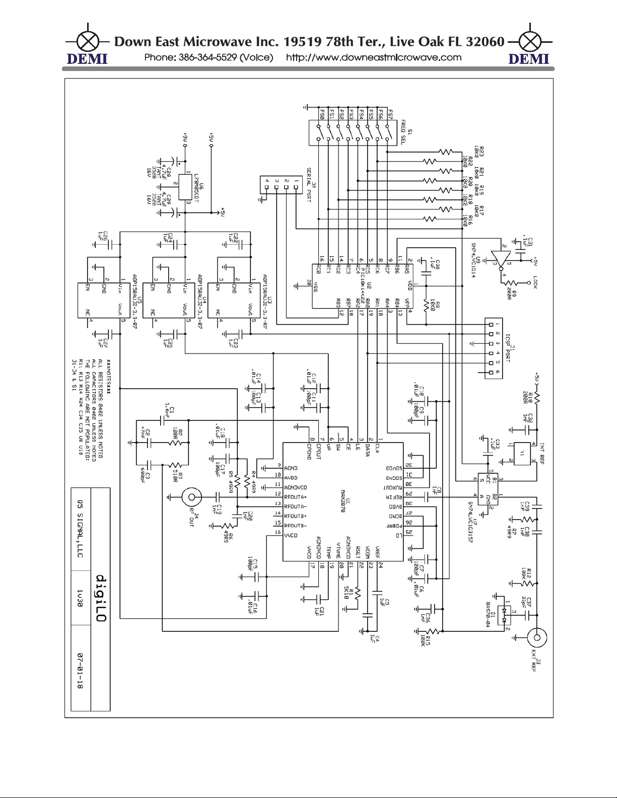
digiLO – A Wideband PLL Synthesizer
The digiLO is a Wideband Fractional-N / Integer-N PLL Synthesizer based on Maxim's
MAX2870 capable of generating signals from 23.5MHz to 6GHz. It measures only 2” x 3” and comes
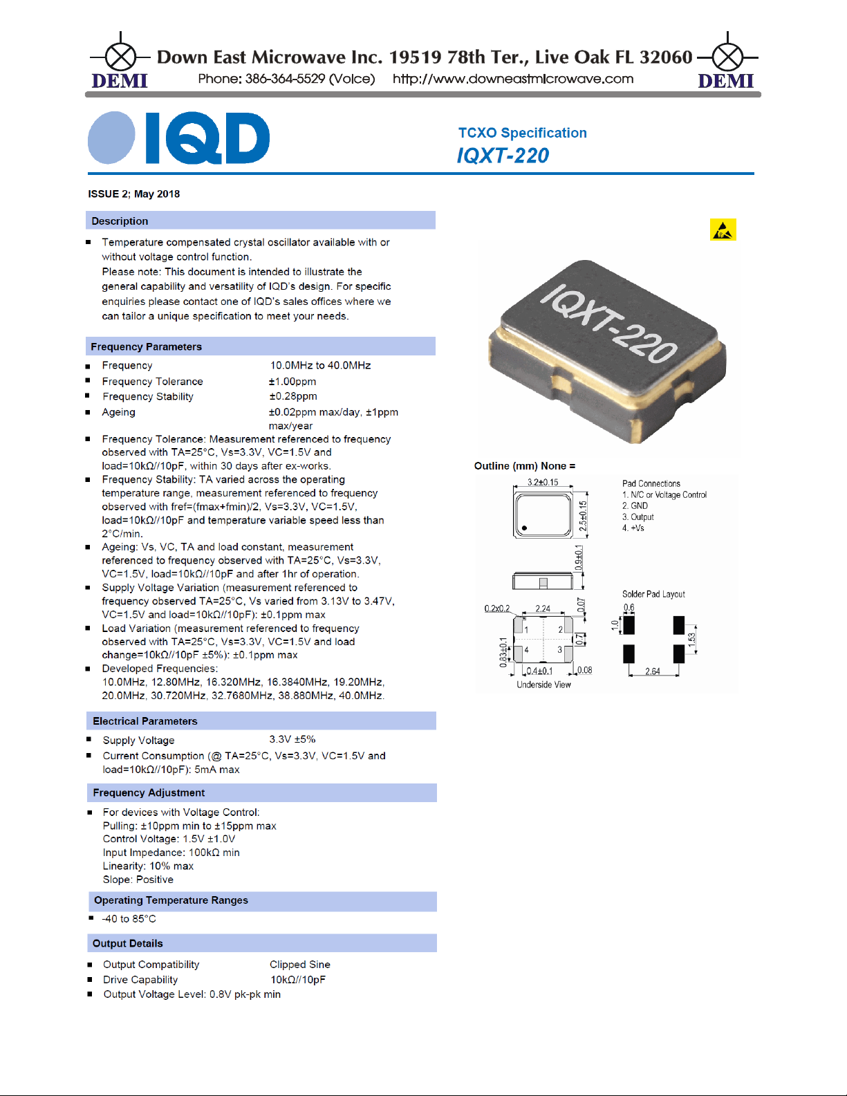
programmed with over a hundre d popular frequencies. A connection to an external 10MH z reference is
provided. But the digiLO automatically switche s to its on-board TCXO reference when its 10MHz
external reference is not detected.
The recommended supply voltage for “+V” is 9V. But reliable operation is possible down to
7V. The digiLO is tolerant of supply voltages up to 15V . But operation beyond 9V results in
excessive heating of the voltage regulator. So if 12V oper ation is desired, it is recommended to use
a 27 Ohm 2-Watt resistor in series with the power connection. This should drop the voltage to the
digiLO to a safer level. A +5V direct connection which bypasses the voltage regulator is al so
available.
The MAX2870's internal volt age controlled oscillator (VCO) operates f r om 3GHz to 6GHz. The
MAX2870 generates output frequencies lower than 3GHz by inserting dividers af ter its VCO up to a
maximum of 1/128. Every divider slightly increases the MAX2870's current consumption. Therefore, the
supply current increases as output frequency decreases. Below 47MHz, supply current is a maximum
of 200mA. And above 3GHz, t he supply current drops to 130mA.
The 10MHz External Reference should be from a clean and stable source. Keep in mind
that the digiLO's output is dir ectly affected by the qualit y of its reference. The recommended input
range for “REF IN” is 0dBm t o + 13dBm. At levels below 0dBm, the digiLO automatically switch es
over to its internal TCXO reference.
When the digiLO is locked to its external 10MHz refer ence , the “LOCK” output switches from 0V
to 5V through a 200 Ohm resistor . This output can also serve as a simple indication of which reference
(external or internal) is so urcing the digiLO. Up to 20mA can be safely sourced fr om this connection.
Therefore, a LED can be connected directly from the “LOCK” output to ground.
The RF output of the digiLO appear s on the “RF OUT” connection. The output level is virtually
flat from 23.5MHz up to 2GHz. And i t maintains a level of +2dBm ±2dB up to 3GHz. Beyond 3GHz,
the output gradually f all s to -10dBm at 6GHz.
Further details of the DIGILO Synthesizer can be found at :
http://q5signal.com/image/catalog/digiLO%20Doc%2018_9_1.pdf
/Built/5760-144rC.docx 13 Rev. C 10/24/2019
Page 14
/Built/5760-144rC.docx 14 Rev. C 10/24/2019
Page 15
/Built/5760-144rC.docx 15 Rev. C 10/24/2019
 Loading...