

Page 1
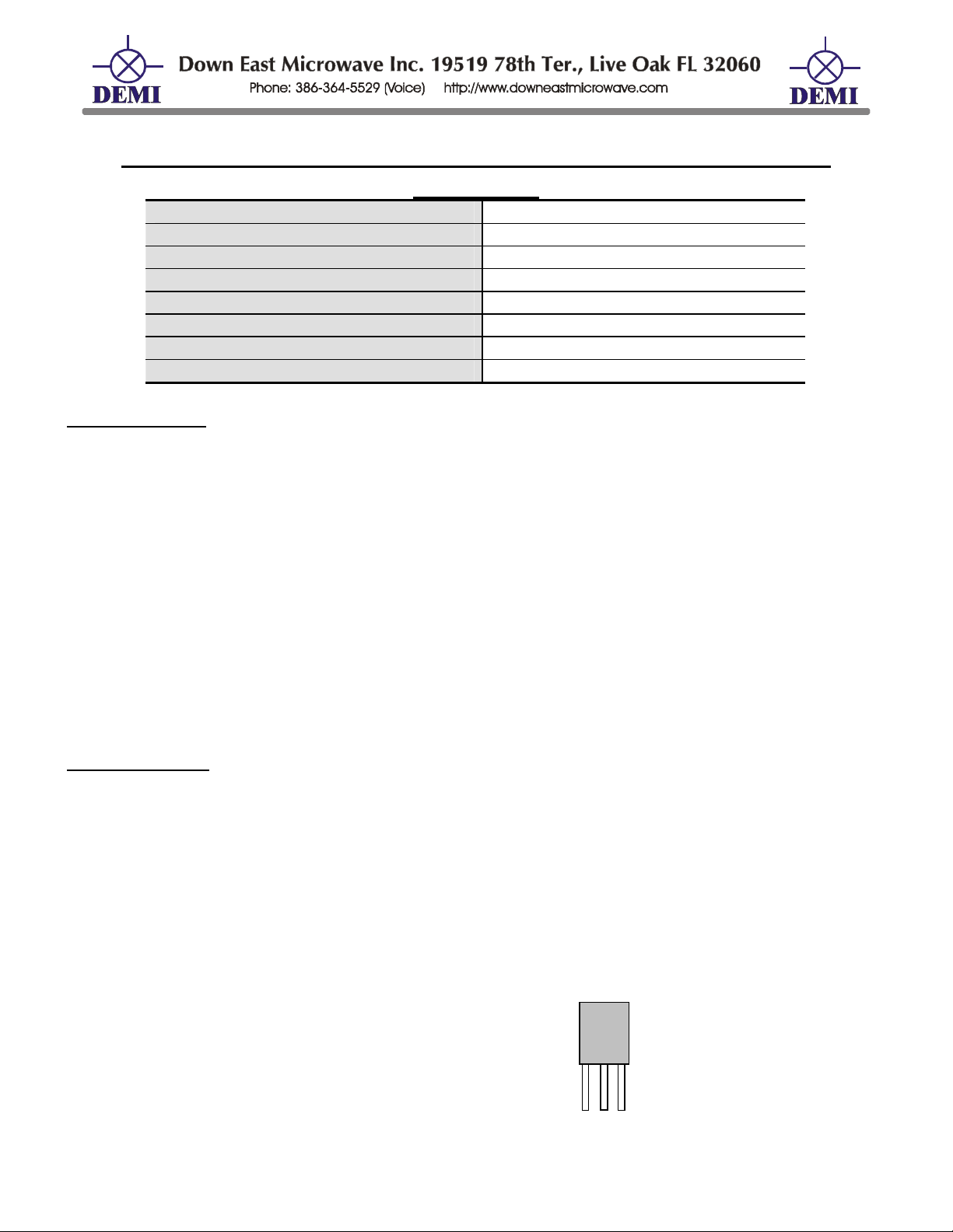
DEM Part Number 2330PAK, CK
30 Watts, 1240 to 1300 MHz Linear Amplifier PCB Kit or Complete Kit
Specifications
Frequency range: 1240 to 1300 MHz.
Power Out (linear): 30 Watts minimum
Power Out (saturated): >40 Watts typical
Power Input for rated power out: 50 mW typical, 75 mW saturated
Power requirements: 13.5 volts dc @ 10.0 amperes MAX.
Connectors: Type-N female
Size with connectors: 5.5" L x 5.5" W x 4.2" H with Fan
Active device: Hybrid RA18H1213G
Kit Description:
The 2330 PAK or CK are simple to build. The PAK is just the circuit board kit. It includes the
PC board and surface mount components. If this is your kit of choice, you will need a heat sink and
be able to configure input and output connectors at the minimum. Coaxial pigtails will suffice only if
good quality coax is used. The DC connections can be made with any wire suitable for the current
consumption of the power amplifier.
If you have the CK or Complete Kit, you have the PAK and all of the hardware and
connectors required to build a complete power amplifier. This also includes a temperature sensitive
cooling fan to ensure reliable 100% duty cycle operation.
Both kits have low current Push-to-talk bias activation circuits (not RF sense) and a simple
relative RF power monitor for ease of setup and operation. Please read over the complete
assembly manual to decide what tools you will need for assembly and to decide what drive option
you may require for your particular system. Review the parts list (s) to identify and inventory. If any
component or procedure is not understood or missing, please contact us before you start. Have
fun with this kit during assembly and use. Good Luck!
Start Assembly:
1. Utilizing the component placement and component list, install all surface mount components
on the circuit board except for R2. The installation of R1 and the value of C1 are determined by
your drive level requirement. See the chart below the component list. Do not install C4, C7, U2,
Q1, or D1. These are the leaded components and need to be prepped before installing. U1 is
installed last.
Be sure to install all surface mount components as flat as possible using whatever
technique makes you feel comfortable. Check all soldered connections when complete.
2. Cut half the length of the leads off U2 and Q1. Then trial fit both of them on the circuit. Bend
the leads in the appropriate positions so the leads may be soldered to the circuit
board. Q1 has the "EBC" leads labeled on the face. U2 is shown here. The labeling
is on the flat surface. D1 is installed as shown. Place the body on the board and
drape the leads over the pads for soldering. Leave excessive lead length on
the body of the diode.
During testing of the complete assembly, the diode may be re-positioned to adjust
the output voltage (higher or lower) if required. C4 and C7 are installed at the final
assembly.
78L05
Out
In
GND
/DEMI/Manuals/Kits/2330pack.doc 1 Rev. B 12/17/2007
Page 2

3. If you only have the PAK version, it is time to mount the circuit board to your heat sink and
make the desired DC and RF connections. After that, skip to the testing section of this document. If
you have the CK version, install the PCB on the heat sink with seven 4-40 x1/4" screws. Snug the
screws but do not tighten. Make sure the PC board is flat on the heatsink. You may find that some
solder has leached through the ground vias and may need to be filed off for best fit.
4. The pins on the "N" connectors are too long for the assembly. First, trim the Teflon on the
connectors with a razor knife to a length of 0.125" (1/8"). This is the thickness of the enclosure
wall. Then trim the pin down to total of 0.375" (3/8"). The total pin length is less important than the
Teflon length. Now install the connectors in the enclosure where the "Half Moon" cutouts are. Use
four, 4-40 x1/4" screws. Do not tighten. Then place the enclosure on the heatsink so that the large
hole in the enclosure is closest to the "PTT-L" label on the PC board. The mounting holes in the
"N" connectors should line up with the holes in the heatsink. Install four, 4-40 x1/4" screws. If the
circuit board interferes with the enclosure assembly, shift its position until it fits. There should be
enough clearance in the total assembly for it all to fit together if the screws are not tight. Once it
fits, center the connectors pins on the input and output lines, then tighten all of the screws (15 of
them). Check for pin alignment and enclosure fit when complete.
5. Find the square black flange connector. Notice the four pins that are installed. The are
labeled 1 through 4. Attach 2" wires as indicated. Pin 1 - #18 colored wire. Pin 2 - #24 wire. Pin 3
- #18 Black wire. Pin 4 - #24 wire. Now, install the connector in the enclosure with four 4-40 x1/4 "
screws. Tighten them. Solder the wires as indicated. Pin 1 to the "+DC" pad. Pin 2 to the "PTT-L"
pad. Pin 3 to the "GND" pad (shown on the component placement diagram). Pin 4 to the "M" pad
(shown on the component placement diagram). Now solder the "N" connector pins.
6. Make up the mating connector. Use a minimum of #14 wire of the DC supply wire for both +
(Pin 1) and - (Pin 3) if the length does not exceed 4 feet. Pins 2 (PTT-L) and Pin 4 (Monitor) can
be any smaller gauge wire that is available. When the mating connector is wired, connect it to the
amplifier for electrical pre-test. Attach the Positive and Negative wires to a 13.8 VDC power supply
or battery. Check the voltage with a voltmeter. Then toggle the PTT-L lead to ground and verify
that there is 5 volts on the bias pad, which would be Pin 2 of U1 on the component placement. If
not check both Q1 and U2. Disconnect supply voltage when test is complete.
6. Un-package U1 and cut the lead lengths in half. Now install U1 by first lightly coating the
flange with thermal compound that was supplied in the kit. A thin, even "see through" covering is
best. Excess compound does not provide better heat transfer. Now inspect and clean the area
where the hybrid attaches to the heatsink. Be sure not to trap anything, no mater how small,
between the heatsink and the hybrid when installing. Place the hybrid into position. While applying
slight downward pressure, slide the hybrid side to side to "seat" it into the thermal compound.
Leave the hybrid in the mounting position with the holes lined up with the flange. Then, find the
brass shield and form it as shown. After forming, place it on
U1. The front part of the shield (shown in the picture)
should fit between the hybrid and the circuit board and
touch the heatsink. Now find the short 6-32 screws and two
#6 flat washers then install them in the flange mounting holes.
Check for pin alignment of U1 and tighten.
/DEMI/Manuals/Kits/2330pack.doc 2 Rev. B 12/17/2007
Page 3

7. Solder the front part of the shield to the circuit board ground between pins 2 and 3 of U1.
You may need to bend the shield out a bit and loosen the two screws in that area of the circuit
board to relieve the "heat sinking" function. Re-tighten screws after soldering. Re-align the pins of
U1 and solder them in place. Install C4 and C7 as close to the hybrid as possible. They may
straddle the chip capacitors if desired.
8. Mount the fan to the assembly by first removing the connector from the fan wires. Then
place the fan on the heatsink with the label up and the fan wires aligned with the odd heatsink hole.
Run the wire through the hole and into the enclosure. Place the guard on top of the fan. Now find
the longest 6-32 screws and four # 6 washers, the run them through the fan and guards mounting
holes down into the enclosure. Use the 6-32 x 1/2" hex stand-offs and install them on the ends of
the fan screws that extend through the heatsink. You may use some sort of thread locking
adhesive for this connection. Tighten the screws snug but do not bend the mounting ears of the
fan. Now shorten, strip and tin the fan wires, then connect them to the circuit pads. Red to +DC
and Black to GND. Do not over heat the wires. They are vinyl and will melt. The amplifier is now
ready to test.
Testing and Instructions for Use:
After testing all coaxial components that will be utilized in the installation, make all RF
connections to the 2330PA. Caution, at 1300 MHz., VSWR and insertion loss become factors
even in the shortest lengths of coax. Never use UHF connectors at 23 cm and keep all coaxial
lengths as short as possible.
Make the DC connections (Pin 1 positive and Pin 3 negative) as before to a 13.8 VDC, 12A
minimum power supply with the assembled mating cable. Apply the DC power to the 2330PA and
observe the fan becoming active. It may be slow at first. Connect a positive lead of a voltmeter to
the Monitor wire (Pin 4) and make the negative lead connection to any ground in the system.
With a proper loads connected to both input and output RF connectors, and No RF drive
applied, activate the PTT-L circuit by connecting the PTT-L (pin 2) and Ground (Pin 3) together.
The amplifier will now have a quiescent current of somewhere between 3 and 6 amps. At this time,
the RF monitor voltage should be checked for zero volts! If not disconnect the PTT-L connection
immediately to verify meter zero. If voltage rises with PTT-L connected and without drive applied,
there may be an oscillation in the amplifier. Re-check all coaxial connections, loads and antennas.
If voltage is zero at all times, verify that there is +5 VDC on Pin #2 of U1. Then verify the presence
of +13.8 VDC on Pin #3 of U1. If all OK, RF drive may be applied.
Apply the drive gradually if possible while monitoring the voltmeter connected to the RF
monitor. During the initial testing, do not exceed the specified drive level for linear operation listed
on the specifications above. If you have installed any of the input drive options, do not exceed the
specified drive level of that option. If you have a power meter in line, you may now calibrate your
system. The voltage will vary with the output power and saturate before the maximum drive level is
obtained. For use, set the output power by adjusting the input drive level.
If the drive level appears to saturate the amplifier to soon, install or change the input
attenuator to the next highest level. The load absorbs the RF power and the small value capacitor
couples a small amount of drive to the input of U1. For levels above 2 watts of drive, you may
need to install additional series capacitance in the input RF line. Remember two capacitors in
series is less than half of the smallest value. Cut the RF line anywhere between the Load and the
input lead of U1, then install the additional low value capacitor. If using the variable capacitor, the
drive level can be increased as the variable is decreased.
/DEMI/Manuals/Kits/2330pack.doc 3 Rev. B 12/17/2007
Page 4

Further Testing:
To increase efficiency, output power, gain and frequency response, additional “snow flaking”
of the output transmission line and adjustment of the input transmission line may be required. This
procedure is purely experimental. It should only be attempted while measuring the output power with
precision test equipment. If sub-standard equipment or antennae with high-reflected power are used
for the additional optimization, it is possible that the amplifier will be matched to different impedances
other than 50 Ohms. CAUTION: Bird wattmeters are not specified for use above 1.0 GHz. even
though you have a 50-watt slug for it. Above 1000 MHz., it is considered relative output power only
and has questionable 50-ohm impedance. Using this type of equipment for optimization could result
into possible oscillations and instabilities when operated into a “Good Load”. Be sure of your test
equipment before attempting.
Adding additional "C" by shunting in the isolated pads on the output circuit will affect the output
power at different frequencies. If you have one specific operating frequency, then optimize for it! If
you wish to "broad-band " the amplifier, you will need to look at a swept response or at least test at
both high and low frequencies, simultaneously to achieve desired results. There may be some
instances where you may need to add a shunt capacitor to the input circuit (low frequency operation)
and adjust for desired results.
Other output power control can be done by reducing the voltage on the control pin (Pin # 2).
This can be done by shunting a resistor in the R2 position creating a voltage divider. A potentiometer
may be substituted for R3 and R2. Do not exceed 1K in value. Pin #2 of U1 draws less than 2 mA. If
the voltage is decreased by more than a volt, linearity my be affected. ALSO- Do not exceed +6 VDC
on the control pin.
The RF monitor output may be adjusted by placing the Hot Carrier diode closer to the RF
transmission line if you want an increase in voltage and further away from the line to decrease the
voltage. If the diode is too close or touching it, it may affect the performance of the amplifier or
damage the diode. Be careful when adjusting its position. It is glass and is fragile. If the reflected
power is high in the antennae system used, the monitor voltage will be higher than normal. It is
advised to have a calibrated reference from a known good 50-ohm load.
If using a power supply with a voltage sense circuit, connect the sense line to the mating connector. This will enable constant voltage to the amplifier under varying drive conditions such as SSB, CW, or AM Video.
Consult the data sheet for the RA18H1213G module on the Mitsubishi Website for further information concerning use and abuse of this hybrid.
Completion:
Install the lid on the enclosure with the four remaining 6-32 screws and 4 rubber feet. Label the
connectors with the supplied labels after cleaning the surface with solution.
Caution:
Do not exceed the rated input power of the standard amplifier or optional RF input by more
than 3 dB. If you make a habit of it, increase or install the input drive option. Do not exceed 15 volts
on the +13.8 VDC connection. Use high quality coaxial cables on both RF connections. Install the
amplifier with the heat sink up so the amplifier will convection-cool and not stress the fans operation.
Do not operate the amplifier without the fan. It is not recommended to keep the amplifier continuously
keyed in any application. Toggle the PTT in transmit only. To not modify the circuit to enable the fan
in transmit only. This will not provide enough cooling for the size of heatsink utilized. Use isolators
when possible and check all new RF connections and antennas.
/DEMI/Manuals/Kits/2330pack.doc 4 Rev. B 12/17/2007
Page 5
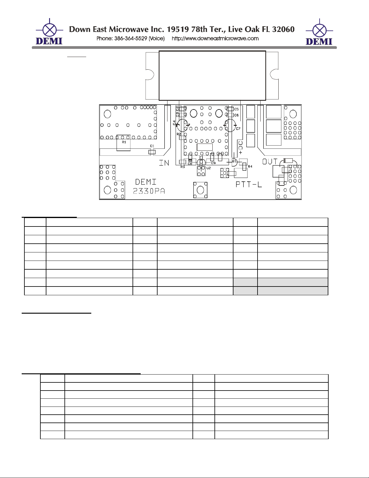
Pin Out
g
1 RF In
2 Bias (TXON)
3 Vcc (+13.8VDC)
4 RF Out
5 RF & DC
round (Flange)
5
12
U1
3
5
4
+
E
B
C
R5
C10
M
D1
C11
R6
optional
+
optional
GND
Component List
C1
C2
C3
C4
C5
C6
C7
C8
C9
100ρF nominal. See chart
0.1 µF chip
100 ρF chip
100 µF elec.
0.1 µF chip
100 ρF chip
330 µF elec. 25V
1.0 µF Tant chip
0.1 µF chip
C10
C11
R1
R2
R2
R3
R4
R5
R6
0.1 µF chip
100 ρF chip
50Ω Load optional
Optional 330Ω
Optional 470Ω
51Ω chip
1KΩ chip
1KΩ chip
1KΩ chip
U1 Power Module
U2 78L05
Q1 MPSW51
D1 HP 2800
C1
C1
0.3-3ρF trimmer
1ρF Chip
Module RF shield
Drive level Chart:
For drive levels below 200 mW, C1 = 100ρF. Do not install R1
For drive level between 200 and 500 mW, C1 = 100ρF and install R1
For drive level between 500 mw and 2 watts, C1 = 0.3-3 ρF variable and install R1
For drive level above 2 watts, C1 = 1 ρF and install R1. The value of C1 may still need to be
adjusted during test.
Additions for Complete Kit (PACK)
2 3/4" Panel "N" connectors 1 Power Amp connector set
4 6-32 x 2-1/2” pan screws 1 Fan w/ guard
4 6-32 x 1-1/4” round screws 1 4” enclosure and lid
2 6-32 x 3/8" pan screws 1 Pre-drilled heat sink
4 #6 hex 1/2" threaded stand-off 1 Heat Sink grease
6 #6 flat washer 4" #24 Teflon wire
4 Rubber feet 4" #18 Teflon wire
20 4-40 x 1/4" pan screws (one extra)
/DEMI/Manuals/Kits/2330pack.doc 5 Rev. B 12/17/2007
Page 6
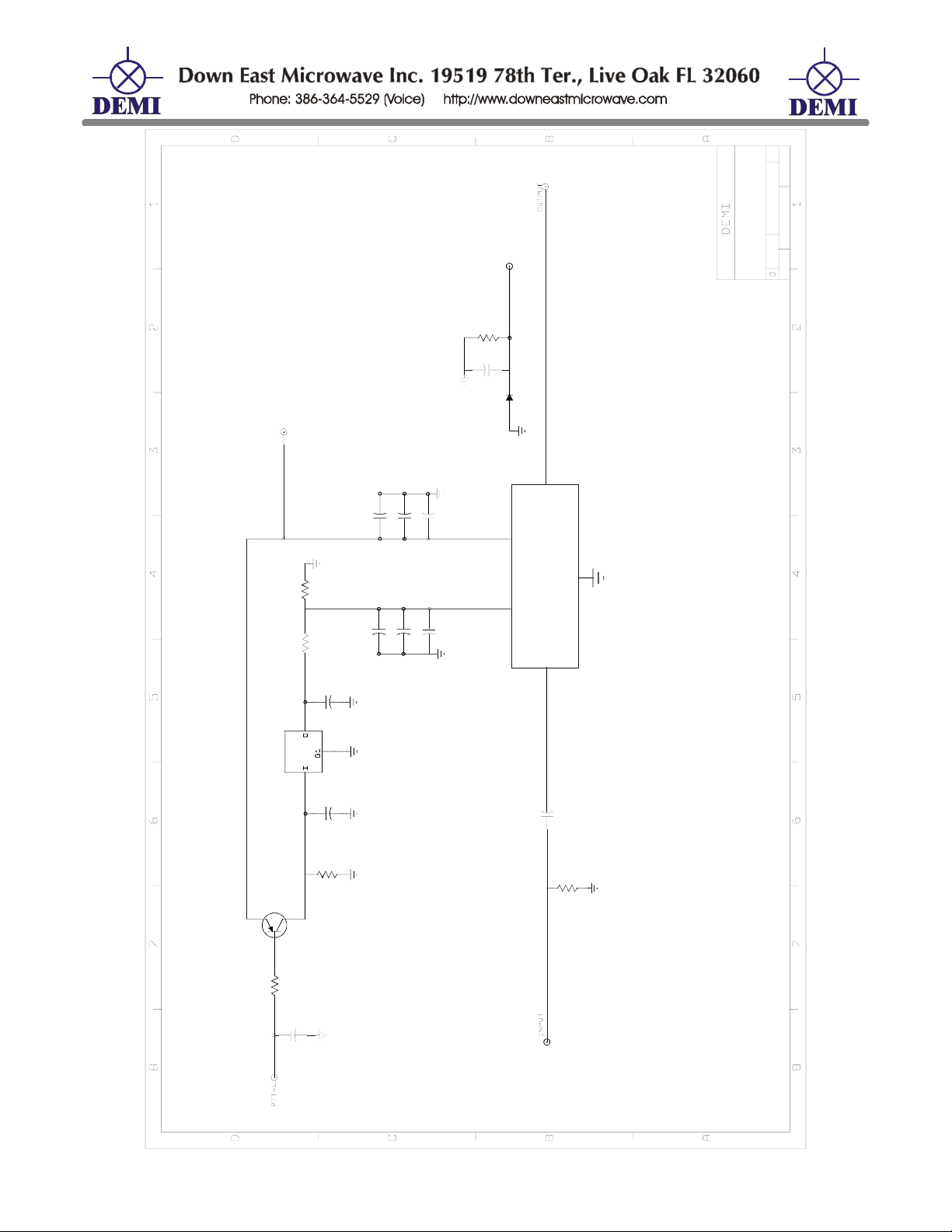
+DC
r
e
i
d
i
f
i
r
l
b
p
y
m
H
A
T
r
E
e
F
s
w
o
o
P
M
03/14/06
Monitor
R6
C11
D1
4
C7
C6
+
C5
3
5
U1
optional
+
C4
C3
R3 R2
C2
2
C8
+
U2
C9
R5
Q1
R4
C10
1
C1
R1
Load
Resistor
optional
/DEMI/Manuals/Kits/2330pack.doc 6 Rev. B 12/17/2007
 Loading...