

Page 1
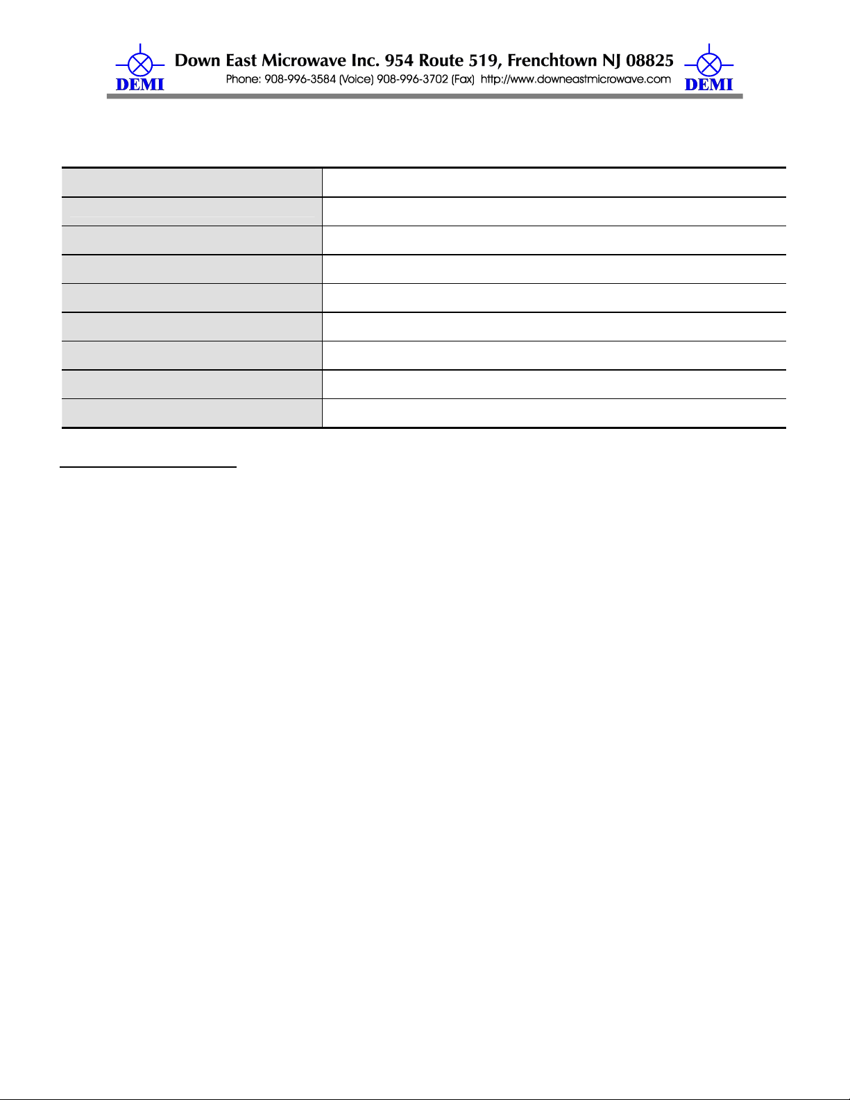
DEM Part Number 222-28
22_____ MHz Transverter, __________ MHz IF, S/N__________
Power Out: 25 W linear, 35 watts maximum; adjustable
Noise Figure and Gain: 0.8dB nominal, +17dB nominal (25 adjustable IF Attenuator)
DC Power Requirement: 12 - 15.5 VDC, 13.8 nominal, 8 amps Maximum
IF Option: Common Split
IF Drive Level Maximum: -20dBm 100 mW 1-10W Other____________
Keying Option: PTT - to ground TTL - Positive Voltage
Aux. Connection Output Option: TX RX High Low Open
Antenna Option: Common Separate TX & RX
External preamplifier option: YES NO
Operational Overview:
The DEM 222-28 is a 222 MHz to 28 MHz transmit and receive converter. It will operate
with most High Frequency transceivers that are available on the market today. The 222-28 has a
linear output power of approximately 25 watts. At full compression, the output power may reach 35
watts, but would be recommended for CW or FM operation only. On the receive side, a GaAs-FET
preamplifier, a high level mixer (+17 dBm Local Oscillator), and a 3 chamber helical filter provide a
sensitive, yet over-load proof front end with superior out of band rejection. The DEM 222-28 has a
built in transmit / receive relay with provisions for external switching so that adding a high power
amplifier to your 222 MHz system is easy. Options have been provided for a key line input of PTT
Low (ground) or PTT High (+Voltage). Auxiliary contacts are included for either transmit or receive
with a common line for many applications. The 28 MHz IF levels are adjustable on both transmit
and receive and have a dynamic range of approximately 25dB. This is very useful for adjusting
your maximum output power and setting the "S" meter level on your IF receiver. IF connections
are via BNC connectors. The control, power, and auxiliary connections are via RCA jacks, and the
222 MHz connectors are BNC, UHF or Type 'N' (users choice). The 222-28 is housed in a 7.4" x
4.7" x 2.2" aluminum die cast enclosure with an external 7" x 4" x 3/4" heat sink to provide cool
operation under any condition.
This transverter, when assembled, has your requested options installed and will be
configured to your transceivers specifications. It is important to fully understand the functions of
your transceiver before interfacing the transverter. Please review your owners manual for any
details regarding transverter operation. If necessary, you may consult us regarding interfacing.
We have not interfaced every transceiver on the market, but could help you in making the correct
decision regarding yours.
/Built/222-28.doc 1 Rev. H 10/11/2005
Page 2
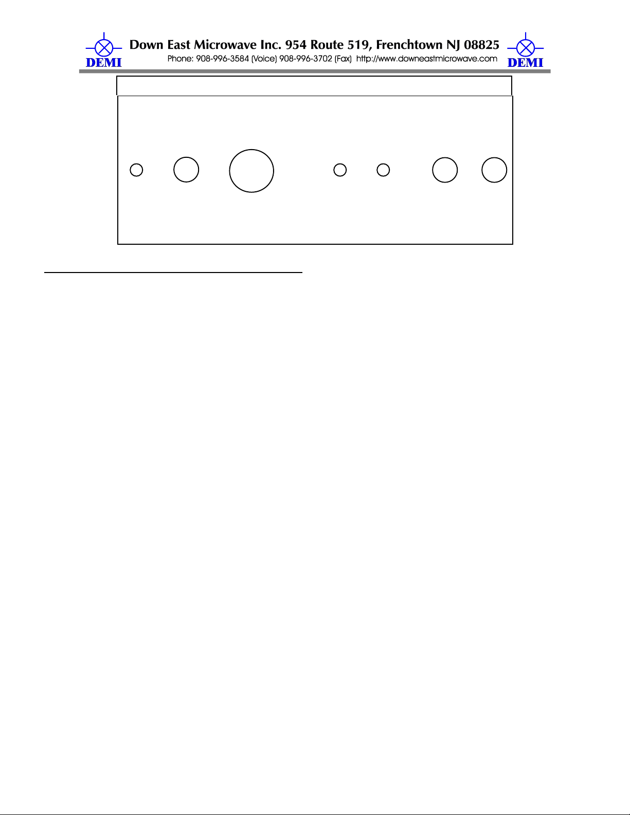
X RX
X
<---------------------- HEAT SINK ----------------------->
RF
XMIT RECEIVE13.8 VDC
PTT- H L AU
IF
T
Connect your transceiver to the transverter:
Interfacing the transverter to the transceiver is easy. If your transceiver requires an
additional interface such as a DEM TIB or AOS, follow those instructions for interfacing. If the
transverter was configured for direct connection to your transceiver, follow the steps listed below.
1. Open lid of transverter by removing 6 screws.
2. Depending on the make and model of your transceiver, it may or may not be necessary to
enable the transverter ports. Follow whatever instructions you have in your transceiver’s
operation manual to enable transverter operation. If it requires a special connector or cable
assembly, it should be made now or contact Down East Microwave for assistance.
3. Connect all IF cables. Both receive and transmit are BNC connections on the transverter. Use
good quality coax cable to connect the 28 MHz. transverter ports from your transceiver to the
TXIF and RXIF connectors on the transverter.
4. Connect the Push to Talk line out of your transceiver to the transverter. It is labeled PTT-H or
PTT-L on the transverter and uses a RCA connector. The correct keying type is already
configured for your transceiver.
5. Connect the 222 MHz. antenna system or a dummy load with a power meter to the transverter.
If one of the “N” connectors is labeled ‘Antenna” then the internal transfer relay in the transverter
is installed. Both transmit and receive functions will be provided through this connector. If the
“N” connectors are labeled “Transmit” and “Receive”, the internal transfer relay has been
bypassed and the separate ports will provide the labeled functions.
6. Connect the DC power to the transverter. It uses a RCA type connector. 13.8 volts is optimum
but the transverter will operate normally from 12 to 15 volts.
7. Preset the TXIF and RXIF gain controls. Turn the TXIF (R7) fully counter-clockwise (maximum
attenuation) and the RXIF (R10) fully clockwise (minimum attenuation).
8. Power your transceiver on and leave it in the Receive mode on 28.100 MHz.
9. Apply power to the transverter and turn on the power switch. The power LED should light and
the transmit LED should not.
10. Adjust the RXIF gain control counter-clockwise until a slight noise increase is heard in the
transceiver or just a slight movement in the “S” meter is detected. Power the transverter on and
off to verify the change. The RXIF gain may be increased beyond this point, but it will start to
degrade the dynamic range of your transceiver. Find a signal on the band or use a signal
generator to determine correct frequency, or minimum signal level. Out of band signals such as
local repeaters will be attenuated if their output frequency is above 224 MHz or below 222 MHz.
11. To test the transmit section, place your transceiver in the CW mode. It is recommended to test
the transverter in the CW mode because most transceivers have carrier level controls in this
/Built/222-28.doc 2 Rev. H 10/11/2005
Page 3
mode only. If your transceiver has FM, it may be use to test the transverter if it has a power
output control. Do not use SSB or AM because it is not possible to obtain maximum output
power with a transceiver in these modes. Set the carrier/output power control to minimum or “0”
output power. Place the transceiver into transmit and verify the transmit LED on the transverter
is lit. While observing the power meter, slowly increase the carrier control (with key down) or
power output control to maximum on the transceiver. If the transverter is configured correctly
for your transceiver, minimal power may be detected on the power meter. Now slowly adjust the
TXIF control in the transverter in a clockwise direction while observing the power meter. Set it
to obtain a maximum of 35 watts. If a power meter is not available, you may use a current
meter on the DC power line to determine if the transverter is transmitting. A maximum of 8
amps should be maintained and it will vary very little as the TXIF control is adjusted. Switch the
transceiver to USB and make a transmission. The power output and current drain should
correlate to your speech pattern.
12. You may re-adjust both RXIF and TXIF again if desired. The adjustments of the receive
preamplifier and local oscillator frequency do not need to be touched but you may if you wish.
Do not adjust any of the helical filters unless you have access to a spectrum analyzer at the
minimum.
13. Put the top on the enclosure and install the screws. Your transverter system is ready to use.
Connect as you wish to use it in your 222 MHz. system and have fun!
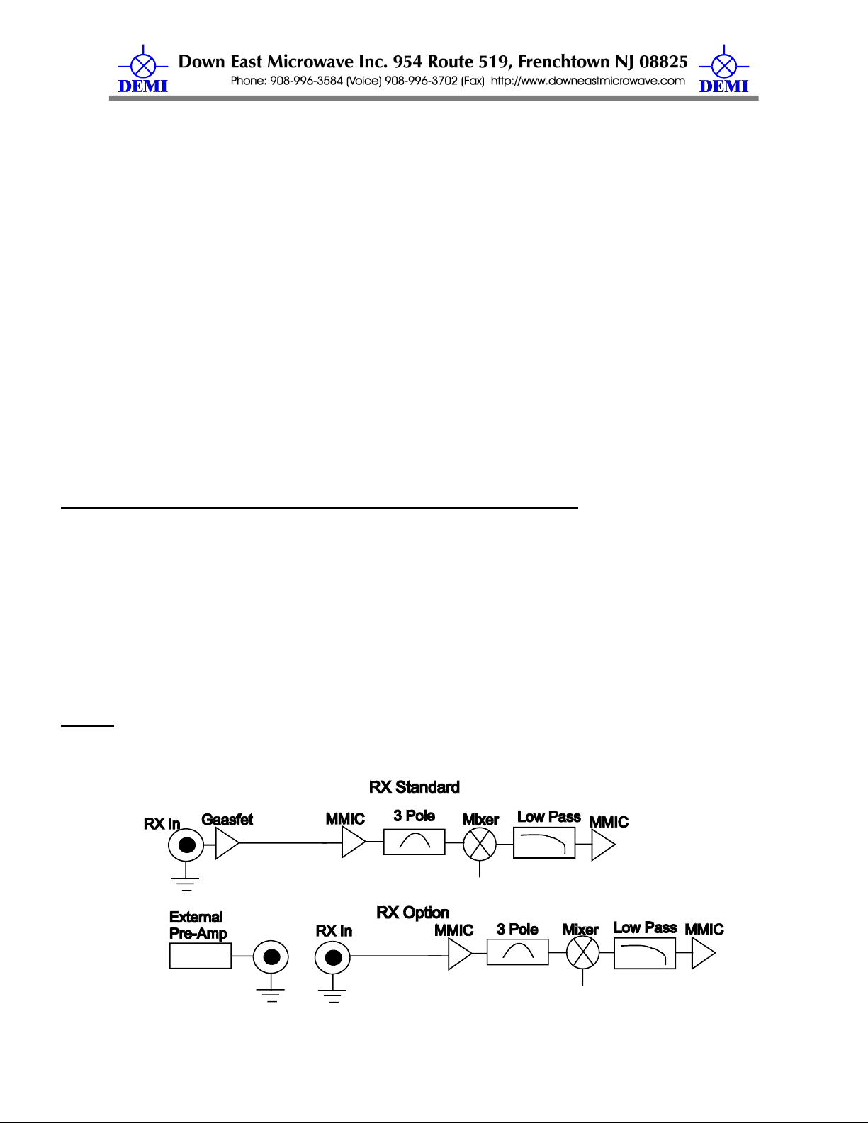
Add an external preamplifier and bypass the internal GaAs-FET:
Below is block diagram of the receive converter. It shows the standard and an option of using an
external preamplifier. It is recommended that if you use a external or mast mount preamplifier, you
should bypass the internal one. The transverter may be configured this way very easily.
1. Refer to the component placement diagram, unsolder, and lift up the end of R24 that is
attached to the pad shared by Q4 and C11.
2. If you do not wish to have the receive signal routed through the T/R relay in the transverter, use
a small length of coax to connect the Q4-C11 pad to the spare BNC connector.
3. If you wish to still use the T/R relay in the transverter, remove C64 from the PCB. Then run a
jumper coax from the pad extending from the relay to the Q4-C11 pad connection.
NOTE: Leaving Q4 connected to the shared pad will offer some minimal attenuation. If you find
this level of attenuation un-acceptable, use solder wick and lift the Drain lead of Q4 up so it is
disconnected from the circuit.
/Built/222-28.doc 3 Rev. H 10/11/2005
Page 4
Auxiliary Switching contacts:
The auxiliary contacts in K1 are labeled C (common) NO (normally open) and NC (normally
closed). The contacts are marked for the receive mode. The C connection can be wired to ground
or +13.8 VDC or any other external signal. The NC and NO connections may then be connected
as desired to he AUX connector. The relay contacts are rated for 3 amps. Do not exceed and it is
suggested that a fuse is installed if you are switching voltage.
DEM 222- 28 User Options
1. Split RX / TX connectors or Common antennae connection
To operate with split TX / RX connectors it is necessary to perform the following modification. If
you have the split option and desire a common connection, reverse the process below.
1. Remove the chip capacitor C64. It is located near the C36 trimmer capacitor.
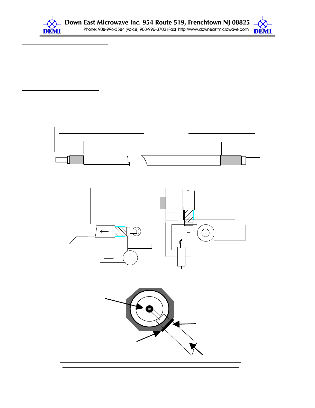
2. Prepare one RG/188 coax as shown in the figure below.
~2.0 - 2 1/2"
1/4"
<= Sh ield
"ANT" END=>
1/2"
3. Remove the coax end attached to the N connector then attachment the RX coax to the
circuit board per the figure below.
RG/188 COAX
CABLE
K2
TO N
1/2" END
TX
TO BNC
1/2" END
ANT
C36
RX
<= NUT NOT SHOWN
4. Route the RX cable to the N connector, remove excess solder from the ground lug and
install the RX coax as shown.
Solder coax center conductor
to connector pin
R33
solder coax shield to
formed lug
Connector
Solder lug
RG/188 coax from PCB "ANT"
PCB MOUNTNG AREA
5. Route the TX cable (old antenna coax) from the antenna position on the PCB to the
BNC connector and solder.
/Built/222-28.doc 4 Rev. H 10/11/2005
Page 5
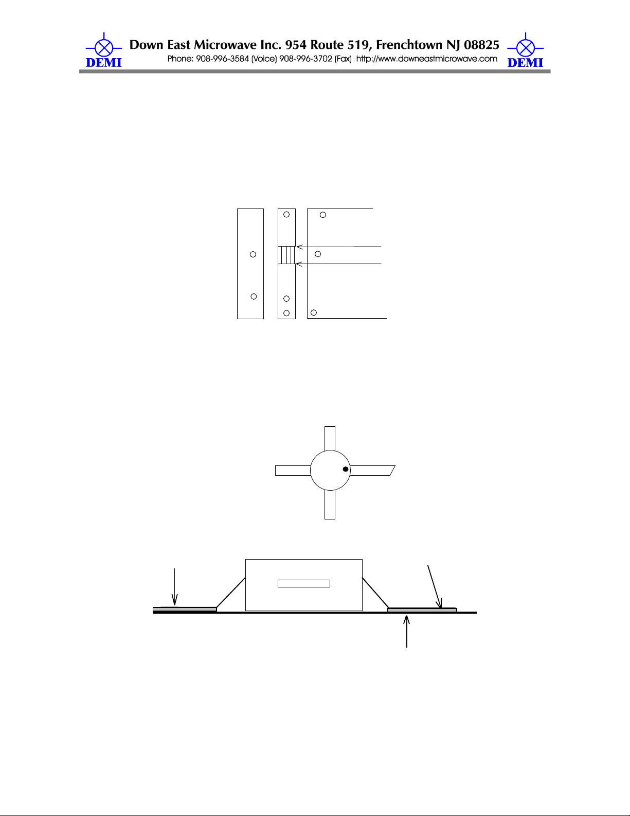
2. Optional Gain Stage
You have the option of installing a additional gain stage (IC4) in the transmit section of the
transverter if you neglected to do so at the time of ordering or if you decide to interface to a
different IF rig. Only consider this option if your transceiver has less than 0dBm output. Please
feel free to consult Down East Microwave Inc. for the proper MMIC and bias resistor. If you elect
to install a gain stage, a modification must be performed to the printed circuit board prior to
continuing. The TXIF path will need to be broken before installation. Referring to the diagram
below and the assembly document, remove the "Ribs" by cutting at the two indicated points with a
sharp razor blade and heating with a soldering iron to remove.
Remove all Ribs Prior
to IC4 Installation
To install, first check the alignment. The DOTS on the MMIC’s determine their orientation and must
be observed and positioned correctly prior to soldering. Align the component in place based on the
component placement diagram. While holding the component in place, solder one lead to hold the
component in place and observe the alignment of all leads. If the alignment is acceptable, solder
the remaining leads. You need enough solder to cover the lead and mounting surface for the
entire lead length.
Input Cut Lea d
IC4
Leads flat to trace, 4 places
Some spring back is OK
Solder shown in shaded areas
Solder full length of lead, 4 places
PCB Trace
Figure 2 Typical side view of four leaded surface mounted device, lead bending close to
body
/Built/222-28.doc 5 Rev. H 10/11/2005
Page 6
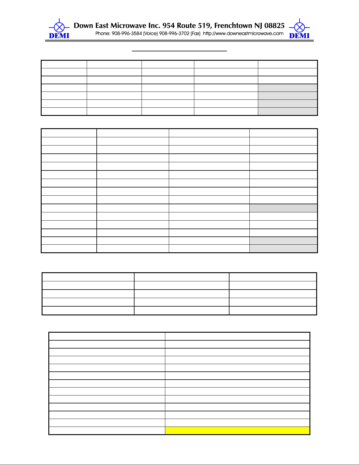
DEM 222-28 Component List
R1 1K R8 220 R16 680 R24 100 1/2W CC R33 1K
R3 1K R9 220 R17 1.5K R25 150 1/2W R35 330 Chip
R5 47 R10 1K POT R18 470 R26 240 R37 51 Chip
R6 100 R11 220 R20 330 R27 47
R7 1K POT R12 220 R21 24 CHIP R28 56 1/2W
R8 220 R14 180 1/2W R22 24 CHIP R29 330
R9 220 R15 150 R23 1K R32 51 Chip
C1 0.1µF (104)
C2 0.1µF C18 0.1µF
C3 1000 (102) C20 120 C40 1-6 Trimmer SMD
C4 1000 C22 1000
C5 1000 C24 1-4 Piston Trim.
C6 1000 C25 1000
C7 1000
C8 120 (121) C27 1000
C9 39
C10 1000
C11 100 CHIP C32 1000
C12 120 C33 270 (271) C50 100 Chip
C13 120 C34 270 C51 120 C77 1000
C14 18 C36 1-6 Trimmer SMD C52 18
C15 22 C37 15 ATC C53 1000
C16 120 C38 18 ATC
C39 15 ATC
C41 0.1µF CHIP C57 0.1µF
C42 0.1µF CHIP C59 0.1µF
C43 2.2µF ELECTR
C26 2.2µF ELECTR
C44 120
C45 100 µF ELECTR
C28 0.1µF C46 0.1µF CHIP
C30 0.1µF
C48 100 Chip C67 120
C49 0.1µF CHIP C68 2.2µF ELECTR
C54 0.1µF
C55 0.1µF
C56 0.1µF
C61 1000
C62 0.1µF
C63 120
C64 100 CHIP
C69 100µF ELECTR
L1 1.0µH (Brown/Black) L10 0.22µH (Red/Red)
L2 0.33µH (Orange/Orange)
L4 0.33µH
L6 0.10µH
L11 3 Turns 3/16" ID (HW)
L12 4 Turns 3/16" ID (HW)
L13 4 Turns 3/16" ID (HW)
L9 3 Turns 1/8" ID (HW) L14 3 Turns 3/16" ID (HW)
L15 3 Turns 3/16" ID (HW
L17 0.22µH
L18 0.22µH
L26 1.0µH
L27 1.0µH
M1 TUF-1H or TUF-1HSM Mixer IC4 MAR6 (optional)
Q1 KN2222 IC7 AG-604
Q2 MPS5179 IC8 MAV11
Q3 2N5179 (Metal Can) VR1 78S09CV
Q4 ATF 21186 VR2 78L09
CR1 1N4000 Type Diode VR3 78L05
CR2 IN914 (Glass Diode) or 1N4148 F1 TOKO 1164A
CR3 MPN3404 F2 TOKO 1146A
CR4 MPN3404 F4 TOKO 1166
K1 G5V-2 Y1 Crystal 194.000 MHz 5th Overtone HC 18/U
CR7 1N4000 Type K2 G6Y
IC1 MAV11 PTC-50 Thermistor
IC2 MAR3 IC5 RA30H2127M
222-28 Common IF Input Circuit Option
/Built/222-28.doc 6 Rev. H 10/11/2005
Page 7
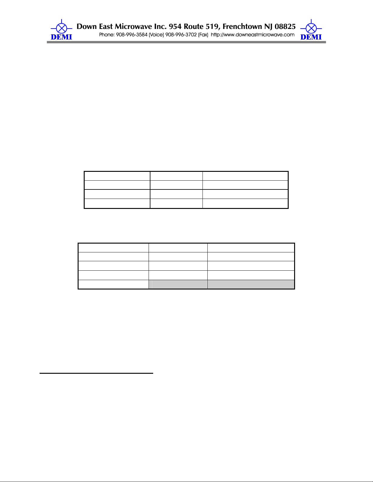
This option is used for common IF input for the 222-28 transverter. There are two versions
of this option. It is a pin switch designed for High and Low Power. The Low Power version is used
with a transceiver that has a less than 250 mW transverter port. If the transverter port has less
than 0 dBm, the transverter will require the TXIF gain stage to be installed. This option should not
be used if drive level is over 1mW. The High Power version should be used with transceivers that
have up to 10 Watts of output. It has a 50-ohm termination mounted on the case for power
dissipation. There is a parts list for each version. The components designators are the same for
both.
Components list to add to the standard components list. All components are shown on the
component placement diagram.
Low Power Option
For transceivers with 250mW or less drive.
C71 1000 Pf C75 100 pF CR10 MPN3404
C72 1000pF C76 1000 pF CR11 MPN3404
C73 1000pF C 1000 pF
C74 100pF
R34 1KΩ
L24 1.0 µH
L25 10T #28 T25-10
High Power Option
For transceivers with greater than 250mW but not to exceed 10 Watts of drive.
C71 4.7 pF C75 100 pF CR10 MA4P1200
C72 1000pF C76 1000pF CR11 MA4P1200
C73 1000pF C 1000 pF
C74 100pF
R34 150Ω 1W
L24 1.0 µH
L25 10T #28 T25-10
R 50 ohm load
The 50-ohm high power resistor is installed on the transverter case. One leg is grounded to
the case the other to the position indicated on the component placement diagram. If you are
installing the option afterwards, you will need to drill a 1/8” hole for mounting. The 1000 pF “C” is
installed from the RXIF BNC connector to the common input indicated on the component
placement diagram. Install a jumper between the TXON pad and the TXOPT pad. Test the
transverter PCB by measuring the junction of R34 and C73 for 0 volts on Receive and +5 volts +/-
0.5 volts on Transmit.
Transverter Operation Overview:
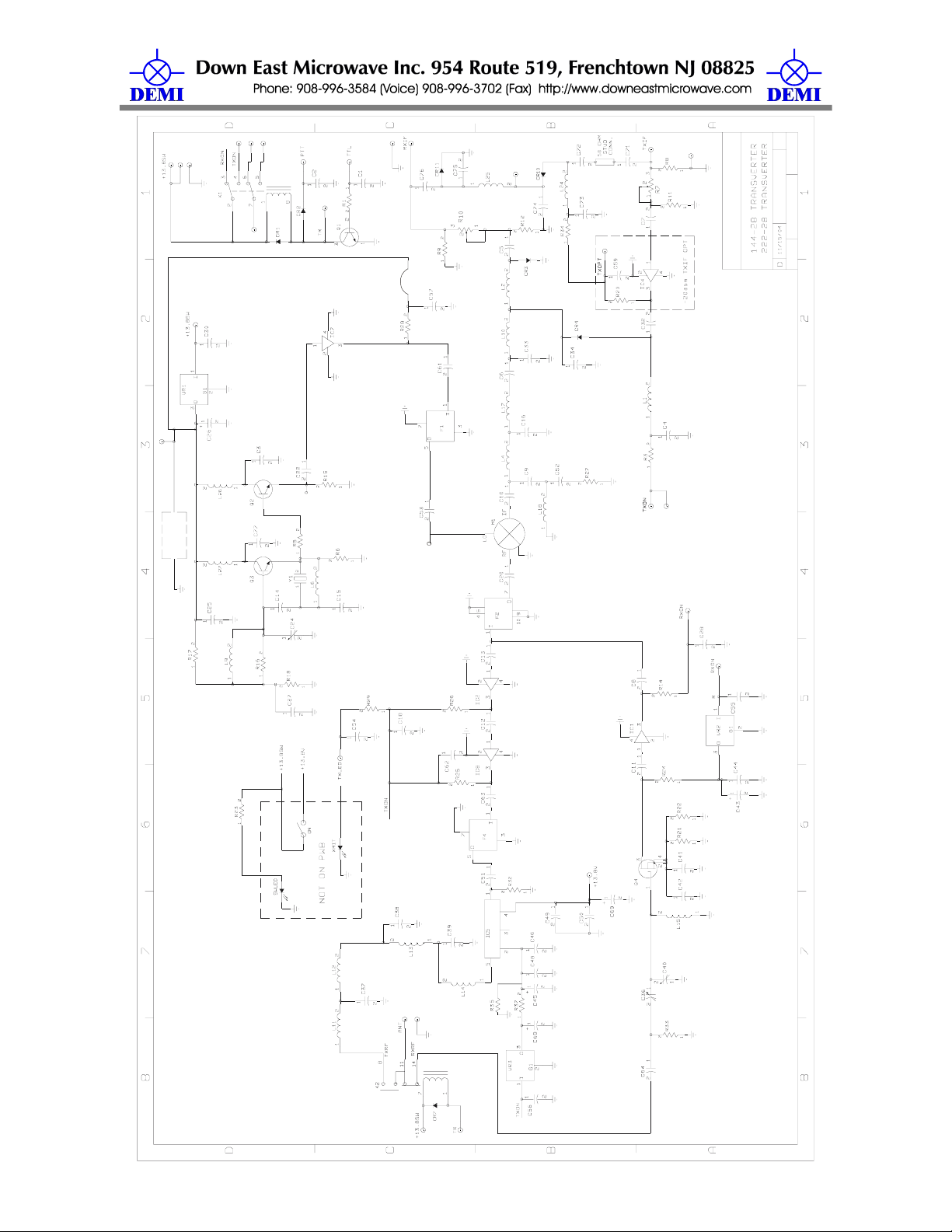
Using the supplied schematic, follow this operation overview for a complete circuit
description. Receive signals enter through a type "N" connector and either pass through
the TR switch (K2) or may go directly to the RX gain stage/filter combination (Q2 and F4).
The gain stage/filter combination, depending on your desired configuration, is quite
versatile. The standard receive line-up is a GaAs-FET preamplifier and a broad band
MMIC (IC6) amplifier separated by a 2 pole 3dB insertion loss helical filter. The GaAs-FET
has a tuned input circuit that is biased to utilize its 1 dB compression point spec. of ≅
+20dBm. Since the FET is designed for microwave frequencies, it has an inherent low
noise figure at the frequency used in this transverter and results in less than 1.0dBNF for
/Built/222-28.doc 7 Rev. H 10/11/2005
Page 8

the system. This signal passes through a 2 pole helical filter that is quite selective and
filters out the out of band signals that may have been amplified by the preamplifier. The
second stage is a MMIC with a 1dB compression point of≅ +18dBm, which amplifies the
filtered signal. In this section, some assembly options may be installed. If you wish to use
a mast-mounted preamplifier, the GaAs-FET (Q4) should be by-passed. There is a
provision on the circuit board for the RX signal to be routed directly to the 2 pole helical
filter (F4) then the MMIC amplifier. Other line-ups may be used such as the GaAs-FET
being the only gain stage in the system before the mixer. With the standard line-up, the
signal then passes through a 3 pole, 5 dB insertion loss, helical filter,(F2) to further
eliminate out of band signals that would cause inter modulation products in the mixer. The
high level mixer (M1) has a +17dBm local oscillator input, which is supplied after passing
through a 2-pole helical band pass filter (F1). This mixer has a 1 dB compression point of
+14dBm and an IP3 (3rd order intercept point) of approximately +29dBm. The mixer is
then terminated into a diplexer band pass filter combination to reduce reflections back into
the mixer further reducing intermod (This is the circuitry between C70 and C76). The IF
signal then enters the IF amplifier stage (IC8) and a adjustable attenuator (R38). This IF
amplifier stage is optional and would only be used if your 28 MHz. receiver can tolerate
signals as high as +15dBm. If a cascade analysis were done with the standard line up, the
math would show that weakest point in the converter system would be the MMIC in the RF
stage (IC6). This means a -10 dBm (71mV) input signal would just start to compress the
converter resulting a system with a IP3 of ≅ +25 dBm and a 1dB compression point of ≅
+15 after the IF gain stage. This is a large signal for anything but some of the newest
and/or best receivers on the market. This level for some of the latter day transceivers
could be as much as 35 dB into compression! The adjustable attenuator has about 25db
of range and could be used to attenuate the IF signal, but could still fall 10 dB short. If the
IF gain stage is not used, there would be maximum of ≅ +2 dBm signal at the input of a 28
MHz. receiver, which is still a large signal!
On transmit, as little as 0dBm will produce a minimum of 10 watts out. If your
transceiver has a lower drive level than that, an optional gain stage may be installed on the
transmit side (IC4). The signal proceeds through an adjustable attenuator, (R35) then
through the same filter diplexer combination as the receive signal. This is done with a pin
diode switch which is biased in the transmit position only (circuitry between C81 and C77).
Although the mixer can handle up to +14dbm before compressing, that level is never
needed or approached. The transmit signal also shares the mixer (M1), 3 - pole helical
filter (F2), and pin diode switch with the receive side (circuitry between C35 and C67). It
then proceeds to a 2-stage amplifier consisting of MMICs (IC4 and IC8). The two stages
have approximately 22 dB gain. The signal is then filtered with a 2-pole helical band pass
filter (F3) with about 3 dB insertion loss. With an +0 dBm IF level entering the transverter
there should be ≅ 50 mW driving the Hybrid module (IC5). The output of the hybrid then
enters a low pass filter to eliminate the 2nd harmonic and above spurious. The signal then
enters the TR switch (K2) or exits the transverter using its own TX port.
All switching functions are controlled by a Signal to Ground or a +1.5-15VDC that is
provided by a transceiver on transmit. The transverter is in RX mode during standby.
Isolated auxiliary contacts are provided for switching external equipment such as mast
mounted pre-amps, power-amps, or T/R switches.
/Built/222-28.doc 8 Rev. H 10/11/2005
Page 9
Common IF
OEM 14 4 / 222 - 28
r
e
p
m
u
J
1
p
T
PTC
2
P
T
/Built/222-28.doc 9 Rev. H 10/11/2005
Page 10
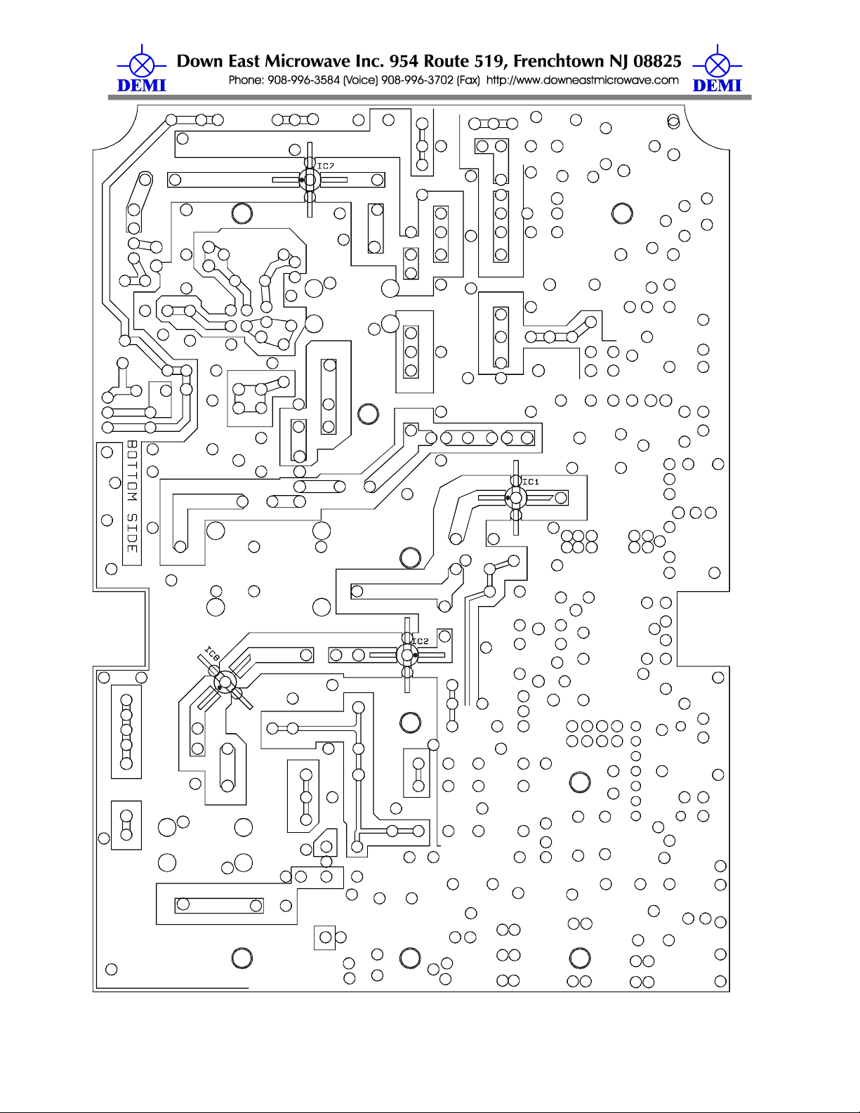
B
o
t
t
o
m
1
4
4
S
/
i
2
d
2
e
2
A
-
s
2
s
8
e
m
b
l
y
/Built/222-28.doc 10 Rev. H 10/11/2005
Page 11

Top Side Assembly
144/222 - 28
T
P
2
/Built/222-28.doc 11 Rev. H 10/11/2005
 Loading...