

Page 1

DEM Part Number 1296-144______
12__________ MHz. Transverter, __________ MHz IF, SN__________
Power Out Maximum: 3 W linear 10mW Other_____________
Noise Figure and Gain: 1.5 dB maximum @ 17 dB conversion gain
DC Power Requirement: 10 - 15.5 VDC @ 2.5 Amp
IF Option: Common Split
IF Drive Level Requirement Option: 1-250 mW 100 mW-1W 1-10W Other_____________
Keying Option: PTT - to ground TTL - Positive Voltage
Aux. Connection Output Option: TX RX High Low Open
Antenna Option: Common Separate TX & RX
Frequency Offset: _________________kHz.
Operational Overview
The DEM 1296-144 is a 23 cm to 144 MHz transmit and receive converter. It has a linear
output power of approximately 3 watts and may be achieved with as little as 10 mW or a maximum
of 10 W of IF drive with the correct IF configuration. The highlight of this transverter is the receive
section. The design uses a PHEMT that has a high-pass tuned input circuit biased for High IP3
output performance. It is followed by two 3 pole helical filters, a high output IP3 MMIC gain stage,
and a high level mixer with a IP3 output of +30 dBm. This design provides a sensitive low noise
receiver with superior out of band signal rejection that will tolerate IP3 input signals > +5 dBm!
Other improvements over the previous versions of 1296 transverters are in the Local Oscillator and
TX section. The base oscillator of the local oscillator circuit is housed in a shielded enclosure on
the circuit board. This shield coupled with the higher frequency base oscillator operation, (192
MHz), reduces the amount of spurious output while providing greater temperature stability. The
transmit section has improved filtering to eliminate all other spurious emissions. The DEM 1296144 has a built in transmit / receive relay on the RF side with provisions for external switching for
adding a high power amplifier or preamplifier to your 23 cm system. The 144 MHz IF levels and
options are adjustable on both transmit and receive with a dynamic range of approx. 25 dB. This is
useful for adjusting your maximum output power and setting the "S" meter level on your IF
receiver. The IF connections are via BNC connectors. Options have been provided for a key line
input PTT-H (+1 to 15 VDC) or PTT-L (a closure to ground) and auxiliary contacts on either
transmit or receive with a common line for many applications. The control, power, and auxiliary
connections are via RCA jacks. The 23 cm connectors are Type 'N' or SMA if separate TX and RX
ports are chosen. The 1296-144 is housed in our standard 4.125" x 1.875" x 7.75" extruded
aluminum enclosure that matches all of our other microwave transverters.
/Built/1296-144.doc 1 Rev. B 12/27/2007
Page 2

Connect your transceiver to the transverter:
Interfacing the transverter to the transceiver is easy. First, review the front page
configuration. If the transverter was configured for direct connection to your transceiver, (10 watts
or less) follow the steps listed below. If you plan on using this transverter with any of the DEMI
transverter interfaces, follow the set-up instructions of that interface. If you have ordered a custom
interface configuration, you already have an idea of what you are doing. Therefore, use the
directions listed below as a guideline.
1. Open the top lid of the transverter by removing the 4 top screws.
2. Connect all IF cables. The transverter may have a common IF port or two separate ports, TXIF
and RXIF. Use good quality coax cable to connect the 144 MHz. ports between your
transceiver and the IF connectors on the transverter.
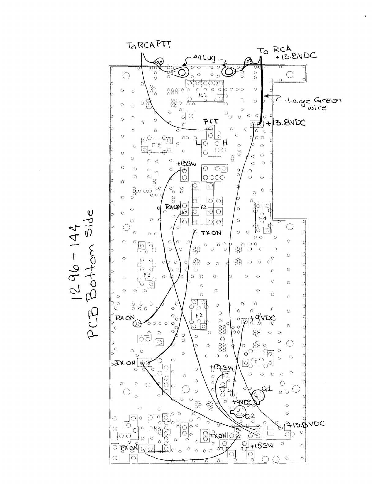
3. Connect the “Push-to-Talk” line out of your transceiver to the transverter. It is labeled PTT-H or
PTT-L on the transverter and uses a RCA connector. The correct keying type can be configured
for your transceiver at time of order or you may select it in the transverter now by moving the
PTT jumper.
4. If separate TX and RX ports were ordered, the internal transfer relay has been bypassed and
the separate “SMA” ports are labeled RX and TX. The “ANT” port has both TX and RX
functions. Connect your 23 cm antenna system or a dummy load with a power meter to the
appropriate 23 cm transverter ports.
5. Connect the DC power to the transverter. It uses a RCA type connector. 13.8 volts is optimum
but the transverter will operate normally from 11 to 15 volts.
6. Preset the TXIF and RXIF gain controls in the transverter. Turn both controls fully clockwise.
This is maximum attenuation on Transmit and minimum attenuation on Receive.
7. Power your transceiver “ON” and leave it in the Receive mode on 144.100 MHz. This should be
1296.100 MHz. unless a frequency offset is indicated on the front page or you ordered a nonstandard transverter.
8. Observe the noise level in the transceiver. If it is too high, adjust the RXIF gain control counterclockwise until a slight noise increase is heard in the transceiver or just a slight movement in the
“S” meter is detected. Power the transverter on and off to verify the change. The RXIF gain
may be increased beyond this point, but it will start to degrade the dynamic range of your
transceiver. Find a signal on the band or use a signal generator to determine correct frequency,
or minimum signal level. If you plan on installing an external LNA, this level will change.
9. It is now recommended to test the transverter in the CW mode because most transceivers have
carrier level or power level controls in this mode only. Do not use full or semi break-in if
possible. Do not use FM, SSB or AM because it may not be possible to obtain maximum output
/Built/1296-144.doc 2 Rev. B 12/27/2007
Page 3

power with a transceiver in these modes. Set the carrier/output power control to minimum or “0”
output power. Place the transceiver into transmit. If the PTT circuit is connected correctly, the
transmit LED on the transverter will switch on. While observing a power meter on the 23 cm
system, slowly increase the carrier control (with key down) or increase the power output control
to the maximum IF drive level indicted on the front page. If you find that the transverter is not
correctly set-up for your transceiver’s range, go to the “IF Options” section at the end of this
page and re-configure the transverter before further testing.
If the transverter is configured correctly for your transceiver, minimal power may be
detected on the 23 cm power meter. Now slowly adjust the TXIF control in the transverter in a
counter-clockwise direction while observing the power meter. Set it to any desired level
between 0 and 3 watts. If a power meter is not available, you may use a current meter on the
DC power line to determine if the transverter is transmitting. A maximum of 2.5 amps should be
obtainable at full output power and it should vary as the TXIF control is varied. Switch the
transceiver to USB and make a transmission. The power output and current drain should
correlate to your speech pattern.
10. You may re-adjust both RXIF and TXIF again if desired. The receive amplifier and local
oscillator frequency should not need to be adjusted but you may if you wish. Do not adjust any
of the helical filters unless you have access to a spectrum analyzer at the minimum.
11. Put the top on the enclosure and install the screws. Your transverter system is ready to use.
Connect as you wish to use it in your 23 cm system and have fun!
DEM 1296 - 144 User Options and performance Improvements:
Auxiliary switching contacts:
The auxiliary contacts in K2 are labeled C (common) NO (normally open) and NC (normally
closed). The C connection can be wired to ground or positive voltage such as the source +13.8
VDC. The K2 common connection will then be toggled depending on what state the transverter is
in. The contacts are marked for the receive mode. The NO or NC can be wired to the AUX
connector on the enclosure.
PTT options:
Both PTT-H and PTT-L can be changed on the topside of the board. The connections are
located in the center of the board near the connector panel. Change the jumper as required from
the PTT connection to either “L” (Ground to transmit) or “H” (Apply positive voltage to transmit)
Add an external preamplifier for noise figure improvement:
If a better noise figure is desired, simply placing a LNA with a modest gain at the antenna
will solve that problem. Understand that the addition of gain in front of this stock transverter will
degrade the IMD performance, and reduce the dynamic range of the transverter by more than the
amount of gain added. You may get a way with doing nothing more than adjusting the RXIF gain
control if you operate in a non hostile RF environment. If your LNA is a ultra low noise unit, it most
likely will not have the IP3 performance the transverter has. It will overload before any component
in the transverter will. So, your receive system now becomes limited by it’s external LNA’s
performance. If you increase the gain performance of your external LNA, (25-30 dB) you may
consider bypassing the transverters LNA completely because it’s IP3 performance is totally
controlled by the external LNA. To do so, remove L5, L31, C59, R31, and R30 from the circuit.
Then connect a short piece of coax between the RX antenna and C63. Be sure to keep it as short
as possible and solder the grounds.
/Built/1296-144.doc 3 Rev. B 12/27/2007
Page 4

Another option is to remove the IF amplifier. If you need to reduce the gain by less than 10
dB, remove IC5 and R18. Then using a 1000 pF disc capacitor, place it across where IC5 was.
You may then adjust the RXIF control to your desired level.
Install / Remove RXIF gain stages:
This was briefly discussed in the external preamplifier section. For whatever reason, you
may require additional gain or have too much IF gain. IC5 can be installed or removed at any time.
Be sure of your systems performance when deciding to make a change. You are also not limited
to the supplied ERA 6 MMIC. You may choose a higher gain unit. The ERA 6 was chosen for its
IP3 output performance. Using this MMIC doesn’t degrade the transverters overall performance. A
high gain MMIC will not only reduce the IP3 by the difference in gain but will also degrade the
system if a lower IP3 output device is used. In the future, this MMIC will change as soon as
something better becomes available.
If changing or removing the MMIC, be sure to add or remove the correct choke and bias
resistor for the desired MMIC. The RXON signal is the same voltage that the transverter operates
on so calculate the new bias resistor based on that voltage.
Add an external power amplifier:
This is the most common addition to this transverter. There are different means in which
this can be implemented. First, determine if your transverter has a common of split RF ports. To
add a power amplifier to a common port transverter will require 2 additional relays on the input and
output of the amplifier to allow the receive signals to bypass the power amplifier. If your
transverter has separate RX and TX ports, you can add the power amplifier in the TX path and
install one relay on the output. This option can be the least troublesome (less relays) and most
cost effective. If you wish to change your transverter from a common to a split RF, see the “RF
Configuration options” section below or the transverter may be returned to the factory for the
modification.
Some power amplifiers have low-level drive requirements. This is accomplished by
disabling the final amplifier stage in the transverter. See “Low Power Option” below.
To key most amplifiers, the set of auxiliary contacts in the transverter may be used. Consult
the “Auxiliary Switching Contacts” section on the proceeding page. If in addition to, you
implement an external LNA, you may consider the use of a Sequencer. Also, consider using
additional filtering or adding a isolator to the system between the transverter and add on power
amplifier for gain and spurious management.
RF Configuration options:
If you wish to change the RF connector configuration, pre-drilled rear panels are available
from DEMI for a nominal fee. They can be supplied with connectors and hardware if required.
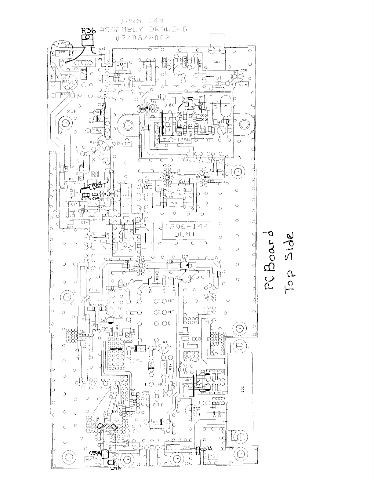
After changing or modifying the connector panel, you will need to move the position of C57, C59,
and L5, for common antenna connection or C57A, C59A, and L5A for a split TX and RX
connections. Re-tuning of the receiver section will be required.
Low Power Option:
If you obtain a power amplifier that requires 20 mW or less drive, the power module, IC9,
may be removed and bypassed. If you do not wish to remove IC9, you will need to lift all four pins
from the connections on the PC board. Then attach a good quality miniature coax between the
input and output pads of IC9. Be sure to solder the shield to ground on both ends. Keep
connections as short as possible. Adjust the output power as before with the TXIF gain control.
/Built/1296-144.doc 4 Rev. B 12/27/2007
Page 5
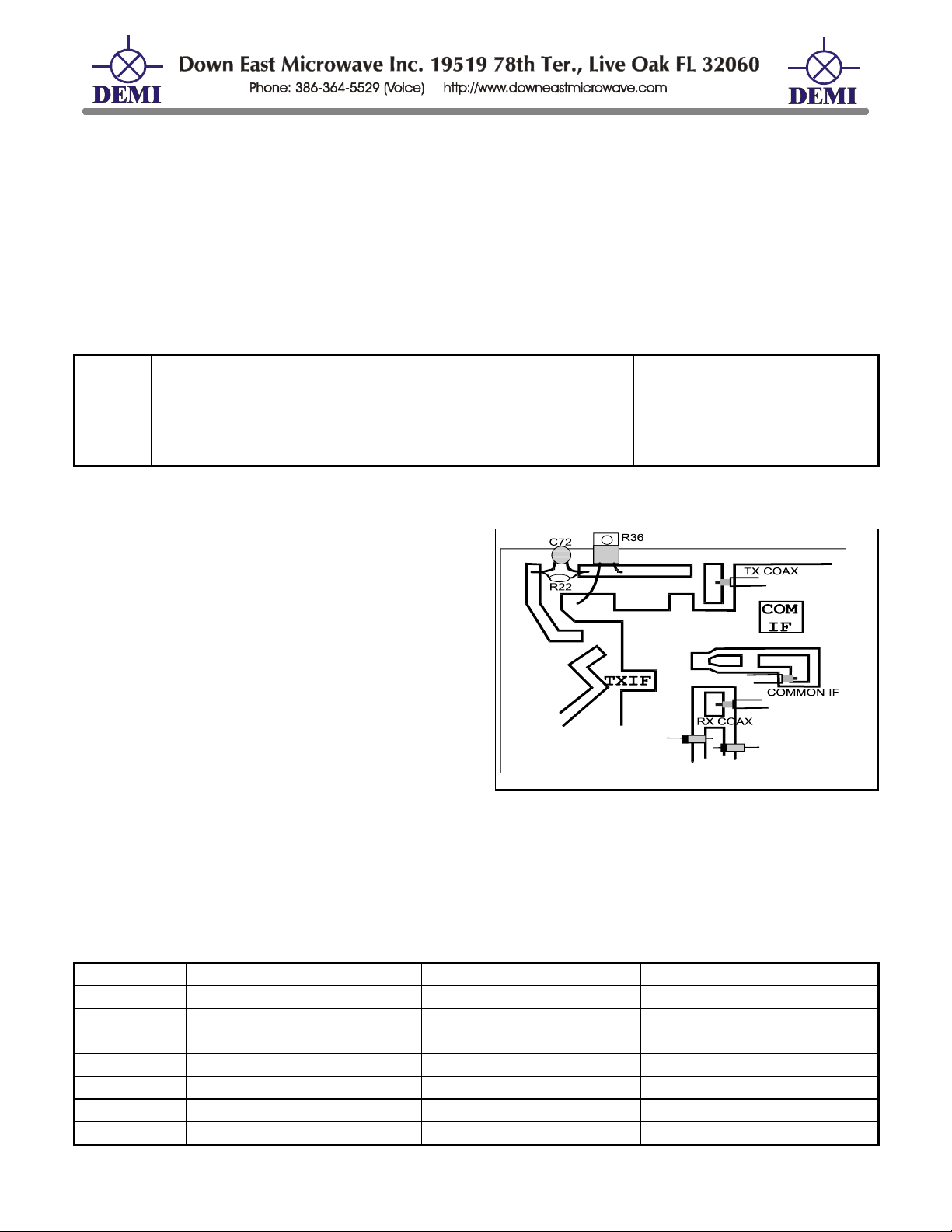
IF options:
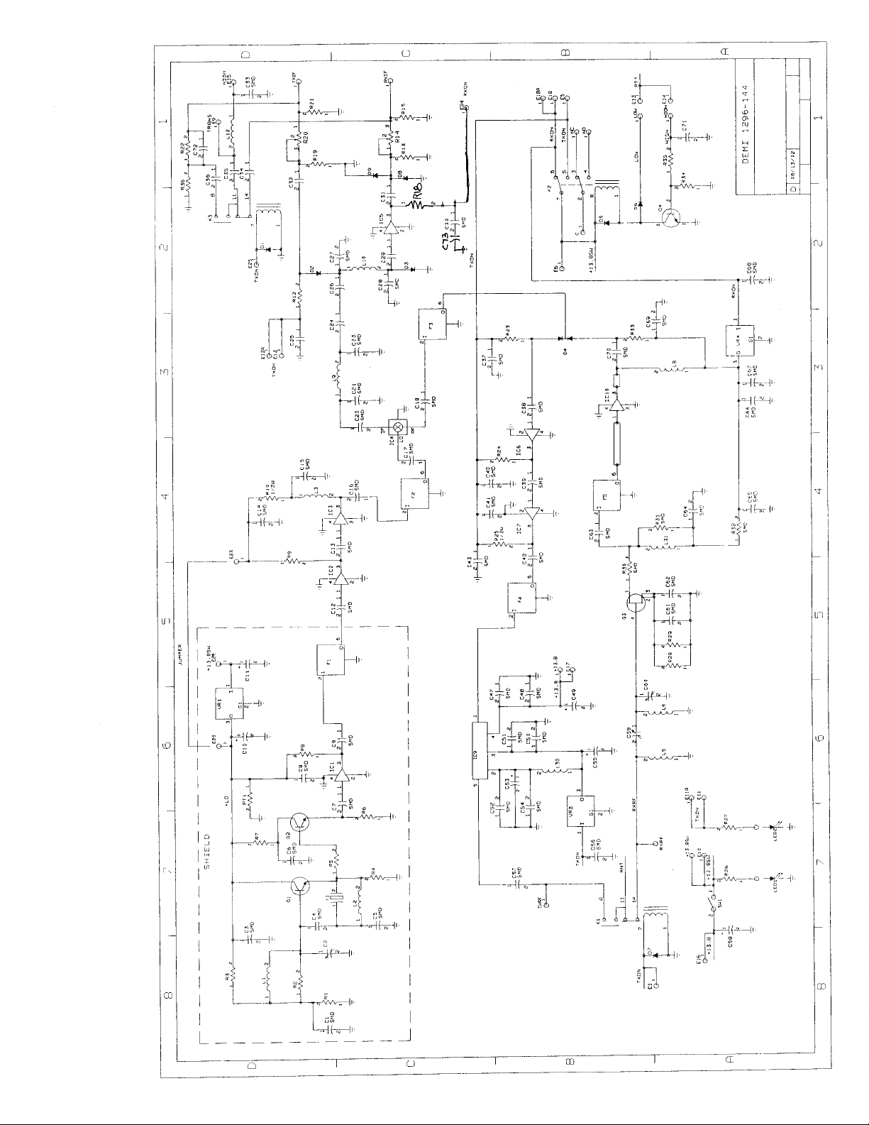
All possible IF configurations are shown below in the supplied schematic and simplified
component layout. Follow the schematic and parts matrix list for desired drive level ranges if you
require a different configuration or drive level. Splitting the IF to separate TX and RX is diagramed
in the simplified component layout below. Other combinations and drive levels may work but do
not exceed 10 Watts of drive level! The 50 Ohm load is rated for 30 watts but only on a heat sink.
The minimum TX drive level for 1 watt of output on 1296 is 1 mW at 144. If you require more
output power or have less IF drive, replace R22 with a short.
1-250mW Drive 100mW-2W Drive 1-10W Drive
C72 Not Installed Not Installed R36 Not Installed R22
220Ω, 1/4W 220Ω, 1/4W
50Ω, 30W 50Ω, 30W
1ρF
Not Installed
Common or Split IF Configuration
DEM 1296 -144 Component List
Resistors (R) values are in Ohms and are chips unless otherwise specified.
R1 470 R9 130 R20 1K POT R28 24
R2 1K R10 56 1/2W leaded R21 220 1/4W leaded R29 24
R3 1.5K R12 1K 1/4 leaded R22 220 1/4W leaded R30 12
R4 100 R13 220 1/4W leaded R23 1K R31 330
R5 51 R14 1K POT R24 330 1/4W leaded R32 12
R6 100 R15 220 1/4W leaded R25 180 1/2W leaded R33 1K
R7 100 R18 150 1/2W leaded R26 1K 1/4W leaded R34 5.1K 1/4W leaded
R8 130 R19 220 1/4W leaded R27 470 1/4W leaded R35 5.1K 1/4W leaded
/Built/1296-144.doc 5 Rev. B 12/27/2007
Page 6
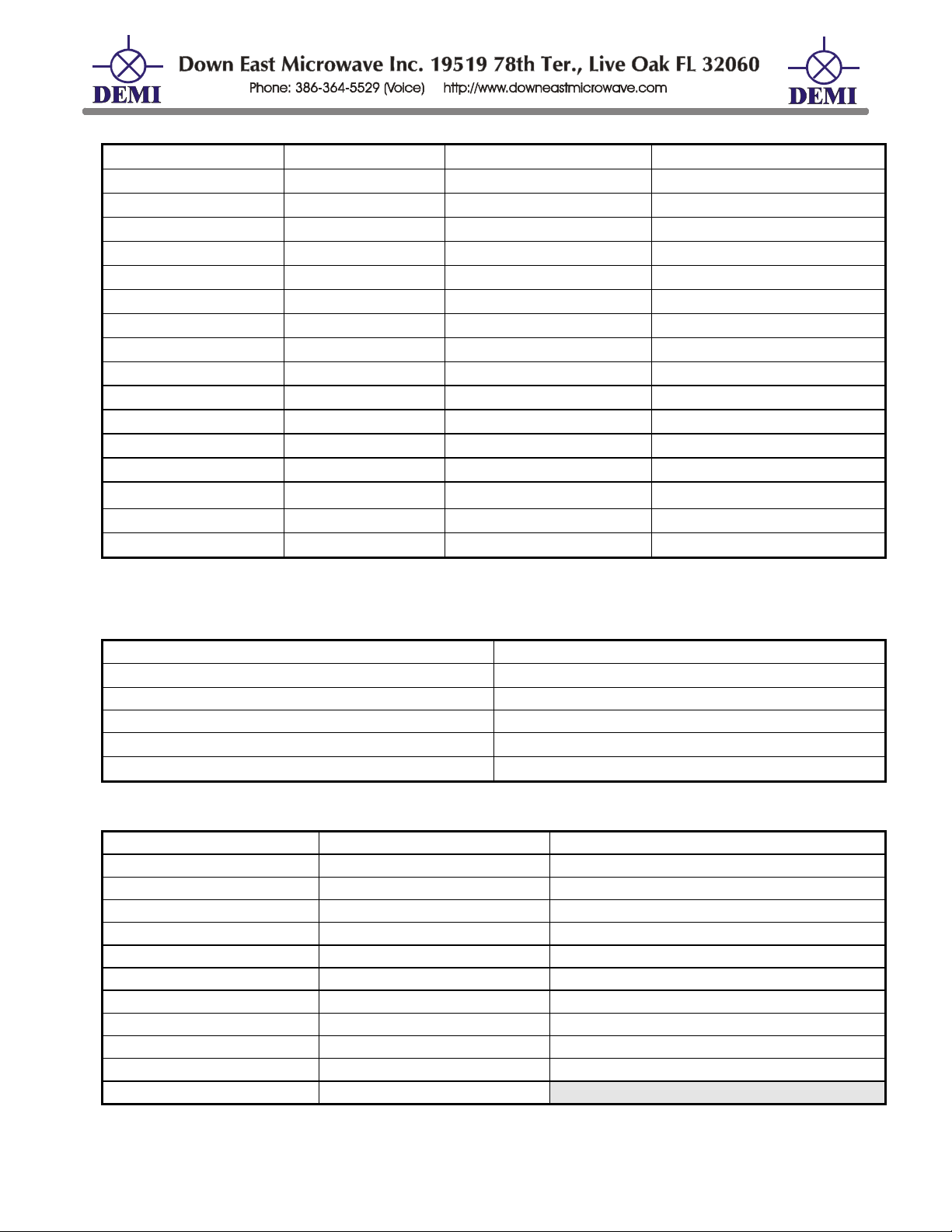
Capacitors (C) values are in ρF and are chips unless otherwise specified.
C1 0.01µF
C18 33
C37 0.01µF
C2 1 - 4 Piston C20 100 C38 33
C3 0.01µF
C4 18 C23 18
C21 18 C39 33 C59, A 0.3-3 VAR.
C40 0.1µF
C5 22 C24 100 C41 33
C6 0.01µF C25 0.01µF
C7 0.01µF
C8 0.1µF
C26 100
C27 18
C42 33
C43 0.1µF
C47 0.1µF
C9 33 C28 18 C48 100
C10 1.0 µF Tant.
C29 100
C49 2.2 µF Elect. C66 1.0 µF Tant.
C11 0.1µF C30 0.1µF C50 0.1µF
C12 33 C31 100 C51 100
C13 33 C32 100 C52 100
C14 0.1µF C33 0.1µF OPT. C53 1.0 µF Tant.
C15 0.1µF
C16 33 C35 100
C17 33 C36 100
C34 100
C54 0.1µF C71 0.01 µF
C55 1.0 µF Tant. C72 1 ρF leaded
C56 0.1µF C73 0.1µF
C57, A 33
C58 100µF Elect.
C60 0.3-3 VAR.
C61 0.1µF 1008
C62 0.1µF 1008
C63 33
C64 33
C65 0.01 µF
C67 33
C68 0.1µF
C69 0.01 µF
C70 33
All inductors are indicated by the enamel wire size,
number of turns, body color, and band colors.
L1 3 Turns 1/8" ID #24 Wire (HW) L8 5 Turns #28 Wire (pre-wound)
L2 0.10 µH (Small body, brown-black)
L3 6 Turns 1/8" ID #24 Wire (HW) L10 5 Turns 1/8" ID #24 Wire (HW)
L5, A 5 Turns 0.05”ID #28 Wire (pre wound) L12 1.0µH OPTIONAL (brown-black)
L6 1T, BLUE Body (pre wound)
L6A 2T, RED Body (pre wound) optional
L9 5 Turns, 1/8” ID #24 WIRE (HW)
L30 0.33 µH(Green body, orange bands)
L31 10 ηH (0603 chip inductor)
Miscellaneous Components
Q1 2N5179 D9 1N914 IC7 MAV11
Q2 2N5179 F1 112570C IC9 M67715
Q3 ATF34143 F2 112570C IC10 AH31
Q4 KN2222 F3 123080C VR1 78S09
D1 1N4000 type F4 123080C VR3 78S09
D2 MPN3404 F5 123080C VR4 78M05
D3 MPN3404 IC1 ERA3 K1 G6Y-1
D4 HSMP 3814 IC2 ERA2 K2 G5V-2
D5 1N4000 type IC3 ERA5 K3 G6Y-1
D6 1N914 IC4 SYM-14H PTC1 PTC 60 Thermistor
D7 1N4000 type IC5 ERA 50 Y1 Crystal 192.000 MHz HC 18/U
D8 1N914 IC6 MAR3
/Built/1296-144.doc 6 Rev. B 12/27/2007
Page 7
Page 8
Page 9
 Loading...