

Page 1

DFZM-E72xx
Data sheet
Data Sheet Sheet 1 of 40 Sep 16, 2013
DFZM-E72xx
An IEEE 802.15.4 System–On-Chip ZigBee
module
Proprietary Information and Specifications are Subject to Change
Page 2

DFZM-E72xx
Contents
1. Features ............................................................................................................................................... 4
2. ZigBee Model No. Definition ............................................................................................................. 6
3. Architecture ......................................................................................................................................... 7
3-1.Block Diagram .............................................................................................................................. 7
3-2.Block Diagram Description .......................................................................................................... 8
3-2-1.Overview ........................................................................................................................... 8
3-2-2.CPU and Memory .............................................................................................................. 8
3-2-3.Clocks and Power Management ...................................................................................... 10
3-2-4.Peripherals ....................................................................................................................... 12
4. Pin-out and Signal Description ......................................................................................................... 15
4-1.Device Pin-out Diagram (Module top view) .............................................................................. 15
4-2.Module Pins Description ............................................................................................................ 16
5. Electrical Characteristics .................................................................................................................. 23
5-1.Absolute Maximum Rating......................................................................................................... 23
5-2.Recommended Operating Conditions ......................................................................................... 23
5-3.Power Consumption.................................................................................................................... 23
5-4.Digital I/O and nRESET Pin Specifications ............................................................................... 25
5-5.Wake-up and Timing ................................................................................................................... 26
5-6.Radio Parameters ........................................................................................................................ 27
5-7.ADC Parameters ......................................................................................................................... 28
6. Package and Layout Guidelines ........................................................................................................ 29
6-1.Recommended PCB Footprint and Dimensions ......................................................................... 29
6-2.Layout Guidelines ....................................................................................................................... 31
6-2-1.Surface Mount Assembly ................................................................................................ 32
6-3.Recommended Stencil Aperture ................................................................................................. 34
7. Ordering Information ........................................................................................................................ 35
8. Package ............................................................................................................................................. 35
8-1.Information of carrier tape direction&packaging dimension ..................................................... 35
8-2.Reel dimension ........................................................................................................................... 37
8-3.Total Package .............................................................................................................................. 38
Data Sheet Sheet 2 of 40 Sep 16, 2013
Proprietary Information and Specifications are Subject to Change
Page 3

Add RF exposure warning statement including FCC
Revision History
DFZM-E72xx
Version
0.1 2013/9/5 Initial release Fred
0.2 2013/9/16
0.3 2014/2/15
Date Reason of change Maker
1. Change the DFZM-E722x module size, and modify all
mechine drawing
2. Add package information
1.
statement.
2. Modify 5.6 Radio Parameter for DFZM-E721x .
Fred
Monch
Data Sheet Sheet 3 of 40 Sep 16, 2013
Proprietary Information and Specifications are Subject to Change
Page 4

DFZM-E72xx
T
DFZM-E72xx
IEEE802.15.4 System-On-Chip ZigBee Module
HIS DOCUMENT describes the DFZM-E72xx ZigBee module hardware specification. The EM357
based modules provide cost effective, low power, and flexible platform to add ZigBee connectivity
for embedded devices for a variety of applications, such as wireless sensors and energy monitoring. It
combines 32-bit ARM Cortex-M3 processor, in-system programable flash memory, 12-KB RAM,
192KB flash memory and off module certified antenna options, and various RF front end options for end
customer range needs in order to provide a ZigBee and regulatory certified. The module has various
operating modes, making it highl y suit for system where ultralow power consumption i s required. Short
transition times between operating modes further ensure low energy consumption.
1. Features
► Family of modules with different antenna and output power options:
• DFZM-E72xx 27 mm by 16 mm by 3.3 mm (Length * Width * Height) 28-pin Dual Flat pack PCB
Surface Mount Package.
• DFZM-E7220, DFZM-E7221, DFZM-E7210, and DFZM-E7211 are all pin to pin compatible (see
section 7 Ordering Information), and the user has to account only for power consumption for various
end applications.
• Simple API for embedded markets covering large areas of applications.
► Compliant with IEEE 802.15.4 and reg ulatory domains:
• RoHS compliant.
► Microcontroller:
• Industry-leading ARM Cortex-M3 processor.
• 192KB Flash with optional read protection.
• 12KB RAM memory.
• Flexible nested vectored interru pt cont ro lle r.
Data Sheet Sheet 4 of 40 Sep 16, 2013
Proprietary Information and Specifications are Subject to Change
Page 5

DFZM-E72xx
► Interfaces:
• Internal antenna or external antenna options.
• Flexible ADC, UART/SPI/TWI serial communications, and general purpose timers.
• Up to 22 configurable general purpose I/Os.
• Single voltage operation: 2.1~3.6V
► Embedded RTC (Real Time Clock) can run directly from battery.
Data Sheet Sheet 5 of 40 Sep 16, 2013
Proprietary Information and Specifications are Subject to Change
Page 6

DFZM-E72xx
1= High Power
0= External Antenna
DT= Delta Define
7=EM357
0~9 then A~Z
Serial no.
2. ZigBee Model No. Definition
D F Z M - E 7 2 2 0 - DT 0 R
E=Pb free
Free-lead
R=RoHS
N=NG
L=Process with Lead
Customer code
Antenna Version
1= Onboard Chip Antenna
Power Version
2= Low Power
Frequency
2= 2.4GHz
Chip Type
Chip Vendor
E=Ember(Silicon Labs)
Product-type
M= Module
Property
Z= ZigBee
Substrate
Company
Data Sheet Sheet 6 of 40 Sep 16, 2013
Proprietary Information and Specifications are Subject to Change
F= FR4
D= DELTA
Page 7
VCC
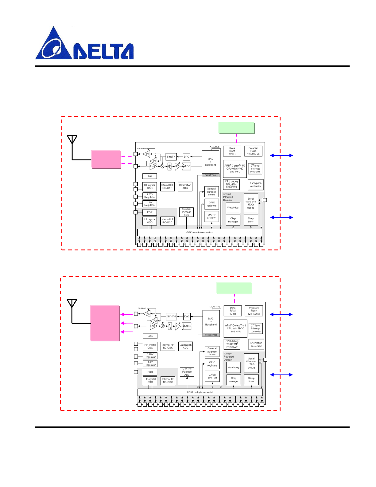
3. Architecture
3-1.Block Diagram
DFZM-E72xx
ANT
ANT
Balun
24M X’tal
Digital I/O
VCC
Figure 3-1: DFZM-E722x Block Diagram
24M X’tal
SE2432L
Figure 3-2: DFZM-E721x Block Diagram
Data Sheet Sheet 7 of 40 Sep 16, 2013
Proprietary Information and Specifications are Subject to Change
Digital I/O
Page 8

DFZM-E72xx
3-2.Block Diagram Description
3-2-1.Overview
DFZM-E72xx module is a highly integrated ZigBee system-on-chip (SOC) that contains the following:
• The module includes Silicon Labs EM357 SoC, which contains CPU- and memory-related,
peripherals-related, clocks and power management-related in a single package.
• The module features an IEEE802.15.4-compliant radio transceiver with onboard 24 MHz crystal circuitries,
RF, and certified antenna or external antenna options.
o The low power module option has a capability of +8dBm output power at the antenna (see Figure
3-1).
o The high power module option has a capability of +18.5dBm output power at the antenna (see
Figure 3-2).
• Variety of interfaces are available such as UART, SPI, TIMER, ADC, Operational amperifier and GPIO.
• DFZM-E72xx contains single power supply (VCC).
3-2-2.CPU and Memory
The EM357 integrates the ARM® Cortex-M3 microprocessor. The ARM® Cortex-M3 is an advanced 32-bit
modified Harvard architecture processor that has separate internal program and data buses, but presents a unified
program and data address space to software. The word width is 32 bits for both the program and data sides. The
ARM® Cortex-M3 allows unaligned word and half-word data accesses to support efficiently-packed data
structures.
The ARM® Cortex-M3 clock speed is configurable to 6 , 12 , or 24 MHz. For normal operation 24 MHz is
preferred over 12 MHz due to improved performance for all applications and improved duty cycling for
applications using sleep modes. The 6 MHz operation can only be used when radio operations are not required
since the radio requires an accurate 12 MHz clock.
The ARM® Cortex-M3 in the EM357 has also been enhanced to support two separate memory protection levels.
Basic protection is available without using the MPU, but normal operation uses the MPU. The MPU allows for
protecting unimplemented areas of the memory map to prevent common software bugs from interfering with
software operation. The architecture could also allow for separation of the networking stack from the application
code using a fine granularity RAM protection module. Errant writes are captured and details are reported to the
Data Sheet Sheet 8 of 40 Sep 16, 2013
Proprietary Information and Specifications are Subject to Change
Page 9
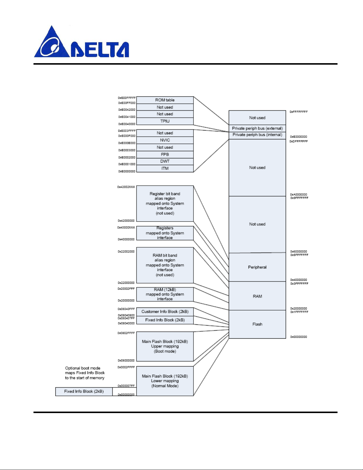
DFZM-E72xx
developer to assist in tracking down and fixing issues. Figure 3.3 shows the EM357 ARM® Cortex-M3 memo ry
map.
Figure 3-3: DFZM-E72xx memory map
Data Sheet Sheet 9 of 40 Sep 16, 2013
Proprietary Information and Specifications are Subject to Change
Page 10
DFZM-E72xx
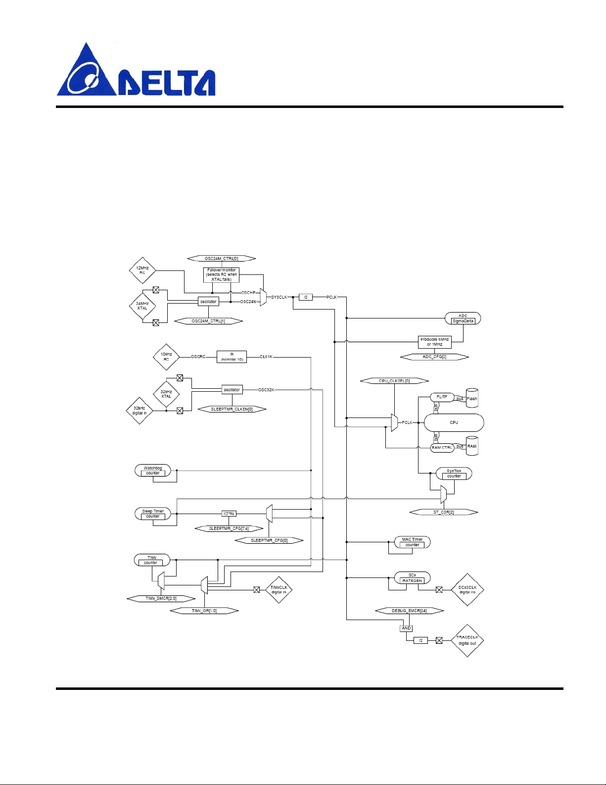
3-2-3.Clocks and Power Management
The DFZM-E72xx integrates four oscillators:
12 MHz RC oscillator
24 MHz crystal oscillator
10 kHz RC oscillator
Figure 3-4 shows a block diagram of the clocks in the DFZM-E72xx. This simplified view shows all the clock
sources and the general areas of the chip to which they are routed
Figure 3-4: DFZM-E72xx block diagram of the clocks
Data Sheet Sheet 10 of 40 Sep 16, 2013
Proprietary Information and Specifications are Subject to Change
Page 11
DFZM-E72xx
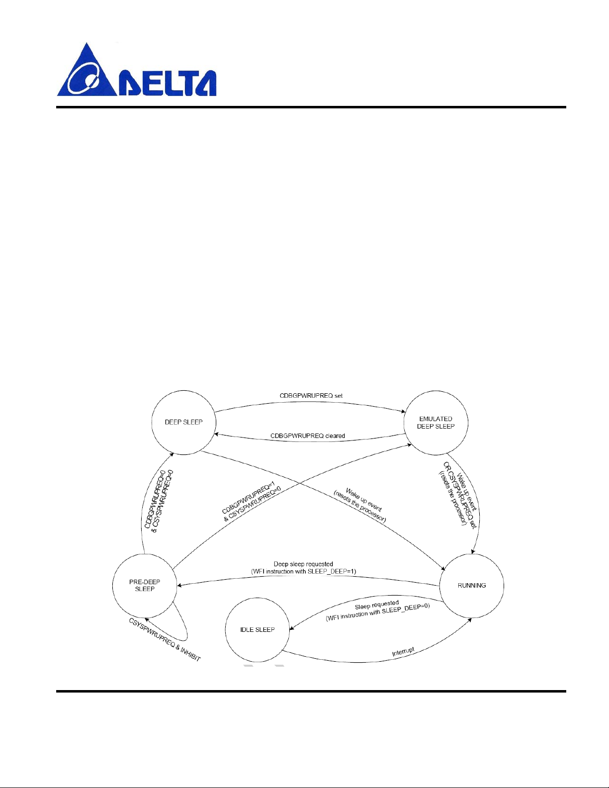
The DFZM-E72xx’s power management system is designed to achieve the lowest deep sleep current consumption
possible while still providing flexible wakeup sources, timer activity, and debugger operation. The DFZM-E72xx
has four main sleep modes:
Idle Sleep: Puts the CPU into an idle state where execution is suspended until any interrupt occurs. All power
domains remain fully powered and nothing is reset.
Deep Sleep 1: The primary deep sleep state. In this state, the core power domain is fully powered down and
the sleep timer is active.
Deep Sleep 2: The same as Deep Sleep 1 except that the sleep timer is inactive to save power. In this mode the
sleep timer cannot wake up the DFZM-E72xx.
Deep Sleep 0 (also known as Emulated Deep Sleep): The chip emulates a true deep sleep without powering
down the core domain. Instead, the core domain remains powered and all peripherals except the system debug
components (ITM, DWT, FPB, NVIC) are held in reset. The purpose of this sleep state is to allow DFZM-E72xx
software to perform a deep sleep cycle while maintaining debug configuration such as breakpoints.
The power management state diagram in Figure 3-5 shows the basic operation of the power management
controller.
Figure 3-5: DFZM-E72xx power management state diagram
Data Sheet Sheet 11 of 40 Sep 16, 2013
Proprietary Information and Specifications are Subject to Change
Page 12

DFZM-E72xx
3-2-4.Peripherals
The DFZM-E72xx has 22 multipurpose GPIO pins, which may be individually configured as:
General purpose output
General purpose open-drain output
Alternate output controlled by a peripheral device
Alternate open-drain output controlled by a peripheral device
Analog
General purpose input
General purpose input with pull-up or pull-down resistor
The GPIO signal assignments are shown in Table 3-1.
GPIO Analog Alternate Output Input Output Current Drive
PA0 TIM2C11, SC2MOSI TIM2C11, SC2MOSI Standard
PA1 TIM2C31, SC2MISO, SC2SDA TIM2C31, SC2MISO, SC2SDA Standard
PA2 TIM2C41, SC2SCLK, SC2SCL TIM2C41, SC2SCLK Standard
PA3 TIM2C21, TRACECLK TIM2C21, SC2nSSEL Standard
PA4 ADC4 P TI_EN, TRACEDATA2 Standard
PA5 ADC5 PT I_DATA, TRACEDATA3 nBOOTMODE
2
Standard
PA6 TIM1C3 TIM1C3 High
PA7 TIM1C4, REG_EN
3
TIM1C4 High
PB0 VREF TRACECLK TIM1CLK, TIM2MSK, IRQA Standard
PB1
TIM2C1
4
, SC1TXD, SC1MOSI,
TIM2C1
4
, SC1SDA Standard
SC1MISO, SC1SDA
PB2 TIM2C24, SC1SCLK
TIM2C2
4
, SC1MISO, SC1MOSI,
Standard
SC1SCL, SC1RX D
PB3 TIM2C34, SC1SCLK TIM2C34, SC1SCLK, SC1nCTS Standard
PB4 TIM2C44, SC1nRTS TIM2C44, SC1nSSEL Standard
PB5 ADC0 TIM2CLK, TIM1MSK Standard
PB6 ADC1 TIM1C1 TIM1C1, IRQB High
PB7 ADC2 TIM1C2 TIM1C2 High
PC0 TRACEDATA1 JRST
5
High
Data Sheet Sheet 12 of 40 Sep 16, 2013
Proprietary Information and Specifications are Subject to Change
Page 13

DFZM-E72xx
PC1 ADC3 TRACED ATA0, SWO Standard
PC2 JTDO6, SWO Standard
PC3 JTDI
PC4 SWDIO
7
5
SWDIO7, JTMS
Standard
7
Standard
PC5 TX_ACTIVE Standard
Notes:
1.Default signal assignment (not remapped).
2. Overrides during reset as an input with pull up.
3. Overrides after reset as an open-drain output.
4. Alternate signal assignment (remapped).
5. Overrides in JTAG mode as a input with pull up.
6. Overrides in JTAG mode as a push-pull output.
7. Overrides in Serial Wire mode as either a push-pull output, or a floating input, controlled by the debugger.
Table 3-1: DFZM-E72xx GPIO signal assignments
The DFZM-E72xx has two serial controllers, SC1 and SC2, which provide several options for full-duplex
synchronous and asynchronous serial communications.
SPI (Serial Peripheral Interface), master or slave
TWI (Two Wire serial Interface), master only
UART (Universal Asynchronous Receiver/Transmitter), SC1 only
Receive and transmit FIFOs and DMA channels, SPI and UART modes
Before using a serial controller, configure and initialize it as follows:
1. Set up the parameters specific to the operating mode (master/slave for SPI, baud rate for UART, etc.).
2. Configure the GPIO pins used by the serial controller as shown in Tables 3-2 and 3-3.
3. If using DMA, set up the DMA and buffers.
4. If using interrupts, select edge- or level-triggered interrupts with the SCx_INTMODE register, enable the
desired second-level interrupt sources in the INT_SCxCFG register, and finally enable the top-level SCx interrupt
in the NVIC.
5. Write the serial interface operating mode (SPI, TWI, or UART) to the SCx_MODE register
Data Sheet Sheet 13 of 40 Sep 16, 2013
Proprietary Information and Specifications are Subject to Change
Page 14

DFZM-E72xx
PB1 PB2 PB3 PB4
SPI-Master
SPI-Slave
TWI-Master
UART
*Note: used if RTS/CTS hardware flow control is enabled.
SC1MOSI Alternate
Output (push-pull)
SC1MISO Alternate
Output (push-pull)
SC1SDA Alternate
Output (open-drain)
TXD Alternate Output
(push-pull)
Table 3-2: DFZM-E72xx SC1 GPIO Usage and Configuration
SC1MISO Input
SC1MOSI Input SC1SCLK Input SC1nSSEL Input
SC1SCL Alternate
Output (open-drain)
RXD Input nCTS Input
SPI-Master
SPI-Slave
SC2MOSI Alternate
Output (push-pull)
SC2MOSI Input
PA0 PA1 PA2 PA3
SC2MISO Input
SC2MISO Alternate
Output (push-pull)
SC1SCLK Alternate
Output (push-pull)
(not used) (not used)
1
SC2SCLK Alternate
Output (push-pull)
SC2SCLK Input SC2nSSEL Input
(not used)
nRTS Alternate Output
(push-pull)*
(not used)
TWI-Master
(not used)
SC2SDA Alternate
Output (open-drain)
Table 3-3: DFZM-E72xx SC2 GPIO Usage and Configuration
SC2SCL Alternate
(not used)
Output (open-drain)
Data Sheet Sheet 14 of 40 Sep 16, 2013
Proprietary Information and Specifications are Subject to Change
Page 15

DFZM-E72xx
4. Pin-out and Signal Description
4-1.Device Pin-out Diagra m (Module top view)
Figure 4-1: DFZM-E72xx Device Pin-out Diagram (Module top view)
Data Sheet Sheet 15 of 40 Sep 16, 2013
Proprietary Information and Specifications are Subject to Change
Page 16

DFZM-E72xx
4-2.Module Pins Description
Pins Name Pin Type Description
1 GND Ground Ground
2 PC5 I/O Digital I/O(Not available for DFZM-E721X-DT0R)
3 nRESET I Active low chip reset(internal pull-up)
PA7 I/O Digital I/O, High current, Disable REG_EN with GPIO_DBGCFG[4]
Timer 1 Channel 4 output, Enable timer output with TIM1_CCER
TIM1C4 O
4
TIM1C4 I Timer 1 Channel 4 input, Cannot be remapped
REG_EN O External regulator open drain output, Enabled after reset
PB3 I/O Digital I/O
TIM2C3 O
TIM2C3 I Timer 2 channel 3 i nput, Enable remap with TIM2_OR[6]
SC1nCTS I
5
SC1SCLK O
SC1SCLK I
Select alternate output function with GPIO_PACFGH[15:12]
Disable REG_EN with GPIO_DBGCFG[4]
Timer 2 channel 3 output, En able remap with TIM2_OR [6]
Enable timer output in TIM2_CCER
Select alternate output function with GPIO_PBCFGL[15:12]
UART CTS handshake of Serial Controller 1
Enable with SC1_UART CFG[5], Select UART with SC1_MODE
SPI master clock of Serial Controller 1
Either disable timer output in TIM2_CCER, or disable remap with TIM2_OR[6]
Enable master with SC1_SPICFG[4], Select SPI with SC1_MODE
Select alternate output function with GPIO_PBCFGL[15:12]
SPI slave clock of Serial Controller 1
Enable slave with SC1_SPICFG[4], Select SPI with SC1_MODE
PB4 I/O Digital I/O
Timer 2 channel 4 output, Enable remap with TIM2_OR[7]
TIM2C4 O
6
TIM2C4 I Timer 2 channel 4 input, Enable remap with TIM2_OR[7]
SC1nRTS O UART RT S handshake of Serial Cont roller 1
Enable timer output in TIM2_CCER
Select alternate output function with GPIO_PBCFGH[3:0]
Data Sheet Sheet 16 of 40 Sep 16, 2013
Proprietary Information and Specifications are Subject to Change
Page 17

DFZM-E72xx
Either disable timer output in TIM2_CCER,or disable remap with TIM2_OR[7]
Enable with SC1_UART CFG[5], Select UART with SC1_MODE
Select alternate output function with GPIO_PBCFGH[3:0]
SC1nSSEL I
PA0 I/O Digital I/O
TIM2C1 O
TIM2C1 I Timer 2 channel 1 input, Disable remap with TIM2_OR[4]
7
SC2MOSI O
SC2MOSI I
PA1 I/O Digital I/O
TIM2C3 O
SPI slave select of Serial Controller 1
Enable slave with SC1_SPICFG[4], Select SPI with SC1_MODE
Timer 2 channel 1 output, Disable remap with TIM2_OR[4]
Enable timer output in TIM2_CCER
Select alternate output function with GPIO_PACFGL[3:0]
SPI master data out of Serial Controlle r 2
Either disable timer output in TIM2_CCER, or enable remap with TIM2_OR[4]
Enable master with SC2_SPICFG[4], Select SPI with SC2_MODE
Select alternate output function with GPIO_PACFGL[3:0]
SPI slave data in of Serial Controlle r 2
Enable slave with SC2_SPICFG[4], Select SPI with SC2_MODE
Timer 2 channel 3 output, Disable remap with TIM2_OR[6]
Enable timer output in TIM2_CCER
Select alternate output function with GPIO_PACFGL[7:4]
TIM2C3 I Timer 2 channel 3 input, Disable remap with TIM2_OR[6]
TWI data of Serial Controller 2 , Either disable timer output in TIM2_CCER,
8
SC2SDA I/O
SC2MISO O
SC2MISO I
PA2 I/O Digital I/O
9
TIM2C4 O Timer 2 channel 4 output
or enable remap with TIM2_OR[6], Select TWI with SC2_MODE
Select alternate open-drain output f unction with GPIO_PACFGL[7:4]
SPI slave data out of Serial Controller 2, Either disable timer output in TIM2_ CCER,
or enable remap with TIM2_OR[6], Enable slave with SC2_SPICFG[4],
Select SPI with SC2_MODE, Select alternate output function with GPIO_ PACFGL[7:4]
SPI master data in of Serial Controller 2
Enable slave with SC2_SPICFG[4], Select SPI with SC2_MODE
Data Sheet Sheet 17 of 40 Sep 16, 2013
Proprietary Information and Specifications are Subject to Change
Page 18

DFZM-E72xx
Disable remap with TIM2_OR[7], Enable timer output in TIM2_CCER
Select alternate output function with GPIO_PACFGL[11:8]
TIM2C4 I Timer 2 channel 4 input, Disable remap with TIM2_OR[7]
TWI clock of Serial Controller 2, Either disable timer output in TIM2_CCER,
SC2SCL I/O
SC2SCLK O
SC2SCLK I
PA3 I/O Digital I/O
SC2nSSEL I
TRACECLK O
10
TIM2C2 O
or enable remap with TIM2_OR[7], Select TWI with SC2_MODE
Select alternate open-drain output f unction with GPIO_PACFGL[11:8]
SPI master clock of Serial Controller 2
Either disable timer output in TIM2_CCER, or enable remap with TIM2_OR[7]
Enable master with SC2_SPICFG[4], Select SPI with SC2_MODE
Select alternate output function with GPIO_PACFGL[11:8]
SPI slave clock of Serial Controller 2
Enable slave with SC2_SPICFG[4], Select SPI with SC2_MODE
SPI slave select of Serial Controller 2
Enable slave with SC2_SPICFG[4], Select SPI with SC2_MODE
Synchronous CPU trace clock, Either disable timer output in TIM2_CCER,
or enable remap with TIM2_OR[5], Enable trace interface in ARM core
Select alternate output function with GPIO_PACFGL[15:12]
Timer 2 channel 2 output
Disable remap with TIM2_OR[5], Enable timer output in TIM2_CCER
Select alternate output function with GPIO_PACFGL[15:12]
TIM2C2 I Timer 2 channel 2 i nput, Disable remap with TIM2_OR[5]
PA4 I/O Digital I/O
ADC4 Analog ADC Input 4, Select analog function with GPIO_PACFGH[3:0]
Frame signal of Packet Trace Interface (PTI)
PTI_EN O
11
TRACEDATA2 O
Disable trace interface in ARM core, Enable PTI in Ember software
Select alternate output function with GPIO_PACFGH[3:0]
Synchronous CPU trac e data bit 2
Select 4-wire synchronous trace interface in ARM core
Enable trace interface in ARM core
Select alternate output function with GPIO_PACFGH[3:0]
Data Sheet Sheet 18 of 40 Sep 16, 2013
Proprietary Information and Specifications are Subject to Change
Page 19

DFZM-E72xx
PA5 I/O Digital I/O
ADC5 Analog ADC Input 5, Sele c t a nalog function with GPIO_PACFGH[7:4]
Data signal of Packet Trace Interface (PTI)
PTI_DATA O
12
nBOOTMODE I
TRACEDATA3 O
PA6
13
TIM1C3 O
TIM1C3 I Timer 1 channel 3 i nput, Cannot be remapped
14 GND Ground Ground
15 VCC Power Power Supp ly Input
PB1 I/O Digital I/O
I/O
Disable trace interface in ARM core, Enable PTI in Ember software
Select alternate output function with GPIO_PACFGH[7:4]
Activate FIB monitor instead of main program or bootloader when coming out of reset.
Signal is active during and immediately after a reset on nRESET.
Synchronous CPU trac e data bit 3
Select 4-wire synchronous trace interface in ARM core
Enable trace interface in ARM core
Select alternate output function with GPIO_PACFGH[7:4]
Digital I/O, High current
Timer 1 channel 3 output, Enable timer output in TIM1_CCER
Select alternate output function with GPIO_PACFGH[11:8]
SPI slave data out of Serial Controller 1
SC1MISO O
16
SC1MOSI O
SC1SDA I/O
SC1TXD O
Either disable timer output in TIM2_CCER, or disable rem ap with TIM2_OR[4]
Select SPI with SC1_MODE, Select slave with SC1_SPICR
Select alternate output function with GPIO_PBCFGL[7:4]
SPI master data out of Serial Controlle r 1
Either disable timer output in TIM2_CCER, or disable remap with TIM2_OR[4]
Select SPI with SC1_MODE, Select master with SC1_SPICR
Select alternate output function with GPIO_PBCFGL[7:4]
TWI data of Serial Controller 1 , Either disable timer output in TIM2_CCER,
or disable remap with TIM2_OR[4], Select TWI with SC1_MODE
Select alternate open-drain output f unction with GPIO_PBCFGL[7:4]
UART transmit data of Serial Controller 1
Either disable timer output in TIM2_CCER, or disable remap with TIM2_OR[4]
Data Sheet Sheet 19 of 40 Sep 16, 2013
Proprietary Information and Specifications are Subject to Change
Page 20

DFZM-E72xx
Select UART with SC1_MODE
Select alternate output function with GPIO_PBCFGL[7:4]
Timer 2 channel 1 output
TIM2C1 O
TIM2C1 I Timer 2 channel 1 i nput, Disable remap with TIM2_OR[4]
PB2 I/O Digital I/O
SC1MISO I
SC1MOSI I
17
SC1SCL I/O
SC1RXD I UART receive data of Serial Controller 1, Select UART with SC1_MODE
TIM2C2 O
TIM2C2 I Timer 2 channel 2 i nput, Enable remap with TIM2_OR[5]
Enable remap with TIM2_OR[4], Enable timer output in TIM2_CCER
Select alternate output function with GPIO_PACFGL[7:4]
SPI master data in of Serial Controller 1
Select SPI with SC1_MODE, Select master with SC1_SPICR
SPI slave data in of Serial Controlle r 1
Select SPI with SC1_MODE, Select slave with SC1_SPICR
TWI clock of Serial Controller 1, Either disable timer output in TIM2_CCER,
or disable remap with TIM2_OR[5], Select TWI with SC1_MODE
Select alternate open-drain output f unction with GPIO_PBCFGL[11:8]
Timer 2 channel 2 output
Enable remap with TIM2_OR[5], Enable timer output in TIM2_CCER
Select alternate output function with GPIO_PBCFGL[11:8]
SWCLK I/O
18
JTCK I
PC2 I/O Digital I/O, Enable with GPIO_DBGCFG[5]
JTDO O
19
SWO O
Serial Wire clock input/output with debugger
Selected when in Serial Wire mode (see JTMS description, Pin 21)
JTAG clock input from debugger
Selected when in JTAG mode (default mode, see JTMS description, Pin 21)
Internal pull-down is enabled
JTAG data out to debugger
Selected when in JTAG mode (default mode, see JTMS description, Pin 21)
Serial Wire Output asynchronous trace output to debug ger
Select asynchronous trace interface in ARM core, Enable trace interface in ARM core
Select alternate output function with GPIO_PCCFGL[11:8]
Enable Serial Wire mode (see JTMS description, Pin 21), Internal pul l-up is enabled
Data Sheet Sheet 20 of 40 Sep 16, 2013
Proprietary Information and Specifications are Subject to Change
Page 21

DFZM-E72xx
PC3 I/O
Digital I/O, Either Enable with GPIO_DBGCFG[5]
or enable Serial Wire mode (see JTMS description)
20
JTDI I
PC4 I/O Digital I/O, Enable with GPIO_DBGCFG[5]
JTMS I
21
SWDIO I/O
PB0 I/O Digital I/O(Not available for DFZM-E721X-DT0R)
VREF Analog O ADC reference output, Enable analog func tion with GPIO_PBCFGL[3:0]
VREF Analog I
JTAG data in from debugger
Selected when in JTAG mode (default mode, see JTMS description, Pin 21)
Internal pull-up is enabled
JTAG mode select from debugger, Selected when in JTAG mode (default mode)
JTAG mode is enabled after power-up or by forcing nRESET low
Select Serial Wire mode using the ARM-defined protocol through a debugger
Internal pull-up is enabled
Serial Wire bidirectional data to/from debugger
Enable Serial Wire mode (see JTMS description)
Select Serial Wire mode using the ARM-defined protocol through a debugger
Internal pull-up is enabled
ADC reference input, Enable analog fu nct ion with GPIO_ PB CFG L[ 3 :0 ]
Enable reference output with an Ember system function
22
IRQA I E xternal inter rupt source A
TRACECLK O
TIM1CLK I Timer 1 e xternal clock input
TIM2MSK I Timer 2 external clock mask input
PC1 I/O Digital I/O
ADC3 Analog ADC Input 3, Enable analog f unct i on with GPIO_PC CFG L[7:4]
SWO O
23
TRACEDATA0 O
Synchronous CPU trace clock, Enable trace interface in ARM core
Select alternate output function with GPIO_PBCFGL[3:0]
Serial Wire Output asynchronous trace output to debug ger
Select asynchronous trace interface in ARM core, Enable trace interface in ARM core
Select alternate output function with GPIO_PCCFGL[7:4]
Synchronous CPU trace data bit 0
Select 1-, 2- or 4-wire synchronous trace interface in ARM co re
Enable trace interface in ARM core
Data Sheet Sheet 21 of 40 Sep 16, 2013
Proprietary Information and Specifications are Subject to Change
Page 22

DFZM-E72xx
Select alternate output function with GPIO_PCCFGL[7:4]
PC0 I/O
JRST I
24
IRQD I Default external interrup t source D
TRACEDATA1 O
PB7 I/O Digital I/O, High current
ADC2 Analog ADC Input 2, Enable analog function with GPIO_ PBCFGH[15:12]
IRQC I Default external interrupt source C
25
TIM1C2 O
TIM1C2 I Timer 1 channel 2 i nput, Cannot be remapped
Digital I/O, High current, Either enable with GPIO_DBGCFG[5]
or enable Serial Wire mode (see JTMS description, Pin 21) and disable TRACEDATA1
JTAG reset input from debugger
Selected when in JTAG mode (default mode, see JTMS description) and
TRACEDATA1 is disabled, Internal pull-up is enabled
Synchronous CPU trac e data bit 1
Select 2- or 4-wire synchronous trace interface in ARM core
Enable trace interface in ARM core,
Select alternate output function with GPIO_PCCFGL[3:0]
Timer 1 channel 2 output, Enable timer output in TIM1_CCER
Select alternate output function with GPIO_PBCFGH[15:12]
PB6 I/O Digital I/O, High current
ADC1 Analog ADC Input 1, Enable analog function with GPIO_ PBCFGH[11:8]
IRQB I External interrupt source B
26
TIM1C1 O
TIM1C1 I Timer 1 channel 1 i nput, Cannot be remapped
PB5 I/O Digital I/O(Not available for DFZM-E721X-DT0R)
ADC0 Analog ADC Input 0, Enable analog function with GPIO_ PBCFGH[7:4]
27
TIM2CLK I Timer 2 e xternal clock input
TIM1MSK I Timer 1 external clock mask input
28 GND Ground Ground
Timer 1 channel 1 output, Enable timer output in TIM1_CCER
Select alternate output function with GPIO_PBCFGH[11:8]
Data Sheet Sheet 22 of 40 Sep 16, 2013
Proprietary Information and Specifications are Subject to Change
Page 23

DFZM-E72xx
5. Electrical Characteristics
5-1.Absolute Maximum Rating
Conditions beyond those cited in Table 5-1 may cause permanent damage to the DFZM-E72xx, and must be
avoided.
Parameter Minimum Maximum Unit
Supply voltage(VCC) -0.3 3.6 V
Storage temperature range -40 125 ºC
Voltage on any digitai I/O -0.3 VCC+0.3 V
Table 5-1: Absolute Maximum Ratings
5-2.Recommended Oper ati ng C ondi ti ons
Parameter Minimum Maximum Unit
Operating supply voltage(VCC) 2.1 3.6 V
Operating ambient temperature range(TA) -40 +110 ºC
Table 5-2: Recommended Operating Conditi ons
5-3.Power Consumption
Test Conditions: TA=25 ºC, VCC=3.0V
Parameter Test conditions Mim Typ Max Unit
Deep Sleep Current
Quiescent current, internal RC oscillator
disabled
Quiescent current, including internal RC
0.4
0.7
uA
uA
Data Sheet Sheet 23 of 40 Sep 16, 2013
Proprietary Information and Specifications are Subject to Change
Page 24

oscillator
DFZM-E72xx
Simulated deep sleep (debug mode)
current
Reset Current
Quiescent current, nRESET asserted 1.2 2.0
Processor and Peripheral Currents
ARM® Cortex-M3, RAM, and flash
memory
ARM® Cortex-M3, RAM, and flash
memory sleep current
Serial controller current For each controller at maximum data rate 0.2
General purpose timer current For each timer at maximum clock rate 0.25
General purpose ADC current At maximum sample rate, DMA enabled 1.1
RX Current
Radio receiver, MAC, and baseband ARM® Cortex-M3 sleeping, CPU clock set to 12 MHz 22
Total RX current ( = IRadio receiver,
With no debugger activity 300
ARM® Cortex-M3 running at 24 MHz from crystal
7.5 9.5
oscillator Radio and all peripherals off
ARM® Cortex-M3 sleeping, CPU clock set to 12 MHz
3.0
from the crystal oscillator Radio and all peripherals off
mA
mA
mA
mA
uA
mA
mA
mA
MAC and baseband, CPU + IRAM, and
Flash memory )
Boost mode total RX current ( = IRadio
receiver, MAC and baseband, CPU+
IRAM, and flash memory )
TX current
Radio transmitter, MAC, and baseband
Total TX current ( = IRadio transmitter,
MAC and baseband, CPU + IRAM, and
flash memory)
ARM® Cortex-M3 running at 24 MHz 26.5
ARM® Cortex-M3 running at 24 MHz 28.5
max. power out (+3 dBm typical)
ARM® Cortex-M3 sleeping, CPU clock set to 12 MHz
maximum power setting (+8 dBm); ARM® Cortex-M3
running at 24 MHz
maximum power setting (+18.5 dBm); AR M® Cortex-M3
running at 24 MHz
Table 5-3: Poewr Consumption
26.0
43.5 mA
110 mA
Data Sheet Sheet 24 of 40 Sep 16, 2013
Proprietary Information and Specifications are Subject to Change
31 mA
mA
mA
Page 25

DFZM-E72xx
5-4.Digital I/O and nRESET Pin Specifications
T est Conditions: TA=25 ºC, VCC=3.0V
Parameter Test conditions Min Typ Max Unit
Low Schmitt switching threshold
VSWIL, Schmitt input threshold going from high to
low
VSWIH, Schmitt input threshold going from low to
High Schmitt switching threshold
high
Input current for logic 0 IIL -1.0 uA
Input current for logic 1 IIH +1.0 uA
Input pull-up resistor value RIPU 24 29 34 kΩ
Input pull-down resistor value RIPD 24 29 34 kΩ
VOL(IOL = 4 mA for standard pads, 8 mA for high
current pads)
Output voltage for logic 0
>85 °C VOL(IOL = 2 mA for standard pads, 4 mA
for high current pads)
VOH(IOH = 4 mA for standard pads , 8 m A for hi gh
current pads)
Output voltage for logic 1
>85 °C VOH(IOH = 2 mA for standard pads, 4 mA
for high current pads)
0.42 x
VCC
0.62 x
VCC
0
0
0.82 x
VCC
0.82 x
VCC
0.5 x
VCC
0.80 x
VCC
0.18 x
VCC
0.18 x
VCC
VCC V
VCC V
V
V
V
V
Output source current
(standard current pad)
Output sink current
(standard current pad)
Output source current high current pad:
PA6, PA7, PB6, PB7, PC0
Output sink current high current pad:
PA6, PA7, PB6, PB7, PC0
Total output current (for I/O Pads) IOH + IOL 2 mA
IOHS 4 mA
>85 °C IOHS 2 mA
IOLS 4 mA
>85 °C IOLS 2 mA
IOHH 8 mA
>85 °C IOHH 4 mA
IOLH 8 mA
>85 °C IOLH 4 mA
Data Sheet Sheet 25 of 40 Sep 16, 2013
Proprietary Information and Specifications are Subject to Change
Page 26

DFZM-E72xx
Table 5-4: Digital I/O Spe c if ic ations
Parameter Test conditions Min Typ Max Unit
Low Schmitt switching threshold
VSWIL, Schmitt input threshold going from high to
low
VSWIH, Schmitt input threshold going from low to
High Schmitt switching threshold
high
Input current for logic 0 IIL -1.0 uA
Input current for logic 1 IIH +1.0 uA
Input pull-up resistor value RIPU, Pull-up value while the chip is not reset 24 29 34 kΩ
Input pull-down resistor value RIPURESET, Pull-up value while the chip is reset 12 14.5 17 kΩ
Table 5-5: nRESET pin Specifications
0.42 x
VCC
0.62 x
VCC
0.5 x
VCC
0.80 x
VCC
V
V
5-5.Wake-up and Timing
Test Conditions: TA=25 ºC, VCC=3.0V
Parameter Test conditions Min Typ Max Unit
From wakeup event to first ARM® Cortex-M3 instruction
System wake time from deep sleep
Shutdown time going into deep sleep From last ARM® Cortex-M3 instruction to deep sleep mode 5 us
running from 6 MHz internal RC clock Includes supply ramp
time and oscillator startup time
Table 5-6: Wake-up and Timing
110 us
Data Sheet Sheet 26 of 40 Sep 16, 2013
Proprietary Information and Specifications are Subject to Change
Page 27

DFZM-E72xx
5-6.Radio Parameters
Test Conditions: TA=25 ºC, VCC=3.0V
Parameter Min Typ Max Unit Notes
RF Frequency range 2400 2500 MHz
TX/RX specification for DFZM-E722x
Output power(boost mode) 1 8 dBm
Output power -3 5 dBm
Error vector magnitude (EVM) 5 15 %
Frequency error tolerance -30 0 30 ppm
Receiver se nsitivity(boost mode) -102 -87 dBm PER = 1%
Receiver se nsitivity -100 -85 dBm PER = 1%
Saturation(Maximum input level) 0 dBm PER = 1%,
TX/RX specification for DFZM-E721x
Output power 18.5 dBm
Error vector magnitude (EVM) 5 15 %
Frequency error tolerance -30 0 30 ppm
Receiver se nsitivity -102 -100 -94 dBm PER = 1%,
Saturation(Maximum input level) 6 dBm PER = 1%,
Table 5-7: Radio Parameters
Data Sheet Sheet 27 of 40 Sep 16, 2013
Proprietary Information and Specifications are Subject to Change
Page 28

DFZM-E72xx
0.5
5-7.ADC Parameters
T est Conditions: TA=25 ºC, VCC=3.0V
Parameter Min Typ Max Unit
VREF 1.17 1.2 1.23
VREF output current 1
VREF load capacitance 10
External VREF voltage range 1.1 1.2 1.3
External VREF input impedance 1
Minimum input voltage 0
Maximum input vlotage VREF
Single-ended signal range 0 VREF
Differential signal range -VREF +VREF
Common mode range 0 VREF
Input referred ADC offset -10 10
Input Impedence
1MHz sample clock
6MHz sample clock
Not sample
1
10
V
mA
nF
V
MΩ
V
V
V
V
V
mV
MΩ
Data Sheet Sheet 28 of 40 Sep 16, 2013
*Note: The signal-ended ADC measurements are limited in their range and only guaranteed for
accuracy within the limits shown in this table. The ADC's internal design allows for
measurements outside of this range (±200 mV), but the accuracy of such measurements is not
guaranteed. The maximum input voltage is of more interest to the differential sampling where a
differential measurement might be small, but a common mode can push the actual input voltage
on one of the signals towards the upper voltage limit.
Table 5-8: ADC Parameters
Proprietary Information and Specifications are Subject to Change
Page 29

DFZM-E72xx
6. Package and Layout Guidelines
6-1.Recommended PCB Footprint and Dimensions
Figure 6-1: DFZM-E72xx Module Recommended PCB Footprint (in mm)
Data Sheet Sheet 29 of 40 Sep 16, 2013
Proprietary Information and Specifications are Subject to Change
Page 30

DFZM-E72xx
Figure 6-2: DFZM-E72xx Module Dimensions (in mm)
Data Sheet Sheet 30 of 40 Sep 16, 2013
Proprietary Information and Specifications are Subject to Change
Page 31

DFZM-E72xx
6-2.Layout Guideli ne s
Figure 6-3: DFZM-E72xx module onboard antenna keep-out layout guidelines (in mm)
Notes:
1. All Dimensions are in mm. Tolerances shall be ±0.10 mm.
2. Absolutely no metal trace or ground layer underneath this area.
3. It is recommended not to run circuit traces underneath the module.
Keep out area for onboard antenna. All layers on the
PCB must be clear.
(i.e. No GND, Power trace/plane, traces.)
Note: If guidelines are not followed, DFZM-E72xx
range with onboard antenna will be compromised.
4. In performing SMT or manual soldering of the module to the base board, please align the two row of pins.
In addition to the guidelines in Figure 6-3, note the following suggestions:
DFZM-E72xx
• External Bypass capacitors for all module supplies should be as close as possible to the module pins.
• Never place the antenna very close to metallic objects.
• The external dipole antennas need a reasonable ground plane area for antenn a ef f ic iency.
DFZM-E7221; DFZM-E7211 onboard antenna specific
The onboard antenna keep out area, as shown in Figure 6-3, must be adhered to. In addition it is
recommended to have clearance above and below the PCB trace antenna (Figure 6-4) for optimal range
performance.
Data Sheet Sheet 31 of 40 Sep 16, 2013
Proprietary Information and Specifications are Subject to Change
Page 32

DFZM-E72xx
60-180 sec
Room temp.
50 sec max
150
200
245
217
(°C )
60-150 sec
Time
Peak temp
250°c max 10 sec max
245°c±5°c for
10 ~30 sec
Do not use a metallic or metalized plastic for the end product enclosure.
Recommendation is to keep plastic enclosure clearance of 1cm from top and bottom of the DFZM-E72xx
onboard antenna keep-out area, if possible. 5-mm (0.2 in) clearance shall be the minimum as shown in
Figure 6-4.
Figure 6-4 Recommended clearance above and below the PCB trace antenna
6-2-1.Surface Mount Assembly
The reflow profile is shown in Figure 6-5.
Data Sheet Sheet 32 of 40 Sep 16, 2013
Figure 6-5: Reflow temperature profile
Proprietary Information and Specifications are Subject to Change
Page 33

Note:
DFZM-E72xx
1. Perform adequate test in advance as the reflow temperature profile will vary accordingly to the
conditions of the parts and boards, and the specifications of the reflow furnace.
2. Be careful about rapid temperature rise in preheat zone as it may cause excessive slumping of the
solder paste.
3. If the preheat is insufficient, rather large solder balls tend to be generated. Conversely, if performed
excessively, fine balls and large balls will generate in clusters at a time.
4. If the temperature is too low, non-melting tends to be caused in the area with large heat capacity after
reflow.
5. Be careful about sudden rise in temperature as it may worsen the slump of solder paste.
6. Be careful about slow cooling as it may cause the positional shift of parts and decline in joining
strength at times.
Data Sheet Sheet 33 of 40 Sep 16, 2013
Proprietary Information and Specifications are Subject to Change
Page 34

DFZM-E72xx
6-3.Recommended Stencil Aperture
Note: The thickness of the stencil should be 0.15mm over this area.
Figure 6-6: DFZM-E72xx recommended stencil apert ure
Data Sheet Sheet 34 of 40 Sep 16, 2013
Proprietary Information and Specifications are Subject to Change
Page 35

DFZM-E72xx
7. Ordering Information
DEVICE DESCRIPTION ORDERING NUMBER
Extended range module using external antenna DFZM-E7210-DT0R
Extended range module using onboard antenna DFZM-E7211-DT0R
Low power module using external antenna DFZM-E7220-DT0R
Low power module using onboard antenna DFZM-E7221-DT0R
8. Package
8-1.Information of carrier tape direction&packaging dimension
Data Sheet Sheet 35 of 40 Sep 16, 2013
Proprietary Information and Specifications are Subject to Change
Page 36

DFZM-E72xx
3
6
PS
5
4
1
2
6
8
7
Protective Tape
(width=56mm,Thickness=0.5mm)
Adhesive Tape
Carrier tape
Accepted
CUSTOMER:
MODEL:
Q'TY:
DATE:
FQC:
RoHS Compliant
Pb
Components
◆
Quantity:750pcs
Leader
20PCS min
Cover tape
5
4
Trailer
20PCS(min)
1
Reel
Accepted
CUSTOMER:
MODEL:
Q'TY:
DATE:
FQC:
RoHS Compliant
Pb
2
3
6
Unreeling direction
ZL:200620003605.7
ZL:200620003605.7
DFZM-TS210-DT0R
FCC ID : H79DFZM-TS210
YYWWNNNNN
DFZM-TS210-DT0R
FCC ID : H79DFZM-TS210
YYWWNNNNN
DFZM-TS210-DT0R
FCC ID : H79DFZM-TS210
YYWWNNNNN
DFZM-TS210-DT0R
FCC ID : H79DFZM-TS210
YYWWNNNNN
10-DT0R
H79DFZM-TS210
YYWWNNNNN
DFZM-TS210-DT0R
FCC ID : H79DFZM-TS210
YYWWNNNNN
DFZM-TS210-DT0R
FCC ID : H79DFZM-TS210
YYWWNNNNN
DFZM-TS210-DT0R
FCC ID : H79DFZM-TS210
YYWWNNNNN
Data Sheet Sheet 36 of 40 Sep 16, 2013
Proprietary Information and Specifications are Subject to Change
Page 37

DFZM-E72xx
W0
W1
ZL:200620003605.7
規 格 品 名
W1
W0
瑋鋒編號
13" 100*44mm旋轉式圓盤
50.0±1.0
45.0±0.5
RUR-26-3-XL
* 代表顏色編碼 B 黑色 , C 寶藍色 ﹐L 藍色﹐W 白色
8-2.Reel dimension
Data Sheet Sheet 37 of 40 Sep 16, 2013
Proprietary Information and Specifications are Subject to Change
Page 38

8-3.Total Package
DFZM-E72xx
Data Sheet Sheet 38 of 40 Sep 16, 2013
Proprietary Information and Specifications are Subject to Change
Page 39

DFZM-E72xx
8-4. RF exposure warning statement
FCC Label Statement
This device complies with part 15 of the FCC rules. Operation is subject to
the following two conditions:
1. This device may not cause harmful interference, and
2. This device must accept any interference received, including interference that may cause undesired
operation.
Federal Communications Commission (FCC) Statement
15.21
You are cautioned that changes or modifications not expressly approved by the part responsible for compliance
could void the user’s authority to operate the equipment.
15.105(b)
This equipment has been tested and found to comply with the limits for a Class B digital device, pursuant to part
15 of the FCC rules. These limits are designed to provide reasonable protection against harmful interference in a
residential installation. This equipment generates, uses and can radiate radio frequency energy and, if not installed
and used in accordance with the instructions, may cause harmful interference to radio communications. However,
there is no guarantee that interference will not occur in a particular installation. If this equipment does cause
harmful interference to radio or television reception, which can be determined by turning the equipment off and
on, the user is encouraged to try to correct the interference by one or more of the following measures:
-Reorient or relocate the receiving antenna.
-Increase the separation between the equipment and receiver.
-Connect the equipment into an outlet on a circuit different from that to which the receiver is connected.
-Consult the dealer or an experienced radio/TV technician for help.
FCC RF Radiation Exposure Statement:
This equipment complies with FCC radiation exposure limits set forth for an uncontrolled environment. End users
must follow the specific operating instructions for satisfying RF exposure compliance. This transmitter must not
Data Sheet Sheet 39 of 40 Sep 16, 2013
Proprietary Information and Specifications are Subject to Change
Page 40

DFZM-E72xx
be co-located or operating in conjunction with any other antenna or transmitter.
Data Sheet Sheet 40 of 40 Sep 16, 2013
Proprietary Information and Specifications are Subject to Change
 Loading...